JP4673533B2 - Integrated circuit with dedicated and programmable logic - Google Patents
Integrated circuit with dedicated and programmable logic Download PDFInfo
- Publication number
- JP4673533B2 JP4673533B2 JP2001520946A JP2001520946A JP4673533B2 JP 4673533 B2 JP4673533 B2 JP 4673533B2 JP 2001520946 A JP2001520946 A JP 2001520946A JP 2001520946 A JP2001520946 A JP 2001520946A JP 4673533 B2 JP4673533 B2 JP 4673533B2
- Authority
- JP
- Japan
- Prior art keywords
- coupled
- test
- interface
- integrated circuit
- programmable logic
- Prior art date
- Legal status (The legal status is an assumption and is not a legal conclusion. Google has not performed a legal analysis and makes no representation as to the accuracy of the status listed.)
- Expired - Lifetime
Links
Images


Classifications
-
- G—PHYSICS
- G11—INFORMATION STORAGE
- G11C—STATIC STORES
- G11C29/00—Checking stores for correct operation ; Subsequent repair; Testing stores during standby or offline operation
-
- H—ELECTRICITY
- H03—ELECTRONIC CIRCUITRY
- H03K—PULSE TECHNIQUE
- H03K19/00—Logic circuits, i.e. having at least two inputs acting on one output; Inverting circuits
- H03K19/02—Logic circuits, i.e. having at least two inputs acting on one output; Inverting circuits using specified components
- H03K19/173—Logic circuits, i.e. having at least two inputs acting on one output; Inverting circuits using specified components using elementary logic circuits as components
- H03K19/177—Logic circuits, i.e. having at least two inputs acting on one output; Inverting circuits using specified components using elementary logic circuits as components arranged in matrix form
- H03K19/17748—Structural details of configuration resources
- H03K19/1776—Structural details of configuration resources for memories
-
- H—ELECTRICITY
- H03—ELECTRONIC CIRCUITRY
- H03K—PULSE TECHNIQUE
- H03K19/00—Logic circuits, i.e. having at least two inputs acting on one output; Inverting circuits
- H03K19/02—Logic circuits, i.e. having at least two inputs acting on one output; Inverting circuits using specified components
- H03K19/173—Logic circuits, i.e. having at least two inputs acting on one output; Inverting circuits using specified components using elementary logic circuits as components
- H03K19/177—Logic circuits, i.e. having at least two inputs acting on one output; Inverting circuits using specified components using elementary logic circuits as components arranged in matrix form
- H03K19/17724—Structural details of logic blocks
- H03K19/17732—Macroblocks
-
- H—ELECTRICITY
- H03—ELECTRONIC CIRCUITRY
- H03K—PULSE TECHNIQUE
- H03K19/00—Logic circuits, i.e. having at least two inputs acting on one output; Inverting circuits
- H03K19/02—Logic circuits, i.e. having at least two inputs acting on one output; Inverting circuits using specified components
- H03K19/173—Logic circuits, i.e. having at least two inputs acting on one output; Inverting circuits using specified components using elementary logic circuits as components
- H03K19/177—Logic circuits, i.e. having at least two inputs acting on one output; Inverting circuits using specified components using elementary logic circuits as components arranged in matrix form
- H03K19/17736—Structural details of routing resources
- H03K19/17744—Structural details of routing resources for input/output signals
Description
【0001】
【発明の属する技術分野】
本発明は、フィールドプログラマブルゲートアレイのようなプログラム可能論理と、ASIC型デバイス等の専用論理と、該プログラム可能デバイス及び専用デバイスの間の通信のためのインターフェースとを有する集積回路に関するものである。
【0002】
【従来の技術】
半導体業界はより高いレベルの集積度を与える願望に駆り立たれている。より高いレベルの集積度の場合には、シリコンのスペース及びコストが減少され、一方性能及び信頼性が増加される。然しながら、より高いレベルの集積度はより大きな特定性に通ずる。例えば、応用特定集積回路(ASIC)は、しばしば、単に一人の顧客のニーズに役立つに過ぎない高度に特定的なデバイス即ち装置である。
【0003】
フィールドプログラマブルゲートアレイ(FPGA)等のプログラム可能な論理装置は多様性のある集積回路チップであり、それは、ユーザがユーザにとって特定的な機能を実現するために形態特定することが可能なユーザが選択した接続状態を具備する内部的回路論理を有している。プログラム可能論理は多様性のあるものであるが、大型で複雑な機能をプログラム可能論理を包含するシリコンプラットフォーム上にマッピングする場合に寸法、経路付け、ピンアウト安定性の上でかなりの設計上のチャレンジが存在している。
【0004】
プログラム可能論理デバイスは別個の専用デバイスとリンクさせることが可能であるが、それと関連するオン/オフチップ遅延、大きな基板面積、及びコスト高等が存在している。更に、所望の機能を実施するためにプログラム可能論理をプログラミングすることが可能であるが、これは高価な提案であり、且つ結果的に得られる性能は、しばしば、許容可能なものではない。
【0005】
【発明が解決しようとする課題】
従って、プログラム可能論理の柔軟性と専用デバイスの性能及び信頼性とを結合した単一の集積化した装置が必要とされている。
【0006】
【課題を解決するための手段】
フィールドプログラマブルゲートアレイ等のプログラム可能論理と、ASIC型デバイス等の専用デバイスとを単一集積回路上にアンチヒューズを基礎としたインターフェースで一体的に結合させる。プログラム可能論理の技術を使用するコンフィギャラブル即ち形態特定可能な非揮発性メモリが専用デバイスに対するパラメータ設定又はその便利なオンチップのコンフィギュレーション(形態特定)を与える。1実施例においては、プログラム可能論理用のプラットフォームは既存のプログラム可能論理デバイスの半分であり、それはプログラム可能論理を構成する必要性を有益的に取除いている。専用デバイスは業界標準バスに対するバスインターフェース等の複雑であるがしばしば必要とされる機能を実現することが可能であり、一方プログラム可能回路はユーザがカスタム機能を実現することを可能とさせる。同一のチップ上に専用デバイスとプログラム可能論理の両方を配置させることは、回路間での高い処理能力を可能とさせるものであるが、その通信は集積回路チップ内部のものであるので、より多数のI/Oピンを必要とするものではない。
【0007】
プログラム可能論理は、専用デバイス内のクロックネットワークからのみならず入力/出力端子からクロック信号を受取るクロックネットワークを包含することが可能である。従って、プログラム可能論理は専用回路とは独立的な周波数で動作することが可能である。プログラム可能論理用の入力/出力クロック端子は、通常、プログラム可能論理に最も近いチップの1つの側部上にあり、一方専用デバイス用の入力/出力クロック端子は専用デバイスに最も近いチップの反対側上にある。該クロックネットワークはクロック信号をプログラム可能論理及び専用デバイスの両方へ分配させる。
【0008】
専用デバイスとプログラム可能論理との間のインターフェースは、バッファ及びテスト回路を具備する多数の導体を有している。該テスト回路はPMOSテストトランジスタとNMOSテストトランジスタとを有しており、それらのゲートはバッファの出力端子へ結合している。PMOSテストトランジスタは電圧供給源と出力端子との間に結合されており、一方NMOSテストトランジスタは接地供給源と異なる出力端子との間に結合されている。PMOSテストトランジスタの出力端子はインバータの出力端子へ結合している。テストモード期間中、該インバータは電圧供給源へ結合される。PMOSテストトランジスタは該インバータにおけるNMOSトランジスタよりも一層大型である。従って、PMOSテストトランジスタがオフである場合には、該インバータは出力端子を低状態へ駆動するが、PMOSテストトランジスタがオンである場合には、PMOSテストトランジスタは該出力端子を高状態へ駆動する。NMOSテストトランジスタの出力端子は、テスト動作期間中接地供給源へ結合される別のインバータの出力端子へ結合される。NMOSテストトランジスタは該インバータにおけるPMOSトランジスタよりも一層大型である。該テスト回路は、該導体へ結合されているアンチヒューズをプログラミングすることなしに、該バッファのテストを有益的に行うことを可能とさせる。
【0009】
本発明の別の実施例によれば、プログラム可能論理と専用デバイスとの間のインターフェースにおける及びその周辺部周りの入力/出力端子はJTAGレジスタを使用してテストされる。JTAGレジスタを介してのテスト信号の経路は、プログラム可能論理及び専用デバイスの両方の周辺部周り、又は該インターフェースを介し且つ専用デバイスの周辺部周りを通過するように選択可能である。
【0010】
【発明の実施の形態】
図1は本発明の1実施例に基づく集積回路10の概略図である。集積回路10はプログラム可能論理12と専用論理14とを有しており、その各々は外部回路との接続のためのI/Oピンを有している。インターフェース16がプログラム可能論理12を専用論理14へ接続している。集積回路10は、同一のシリコン片上に専用論理14を「埋め込んだ」プログラム可能論理装置として、又は、その逆である、即ち「埋込型」プログラム可能論理12を具備する専用デバイスとして考えることが可能である。プログラム可能論理12は、例えば、フィールドプログラマブルゲートアレイ(FPGA)又はユーザプログラム可能回路接続を具備するその他の回路であり、一方専用論理14は所望の機能を実現する固定した回路である。例えば、専用論理14は業界標準バスとのインターフェースを形成する等の機能を実施する応用特定回路とすることが可能である。
【0011】
図1は、更に、プログラム可能リードオンリメモリ(PROM)18を示している。PROM18は、専用論理14用のパラメータを形態特定又は設定するデータを格納し且つプログラム可能論理12の技術を使用して実現することが可能である。一方、PROM18は同一の目的を達成する外部又は内部のEEPROMで置換することが可能である。
【0012】
有益的なことであるが、接続したプログラム可能論理12及び専用論理14を具備する集積回路10は、ユーザに対して、例えばFPGA等のプログラム可能論理において見出される形態特定可能性及び柔軟性のみならず、ASIC等の専用デバイスにおいて見出される保証された機能性、使用容易性、及び高性能を与える。
【0013】
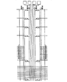
図2はプログラム可能論理12及びインターフェース16の一部の1実施例の1つの大きな簡単化した概略図を形成するためにどのようにして図2A,2B1,2B2,2B3,2C,2D,2E,2F1,2F2,2F3,2G,2H,2I,2J1,2J2,2J3,2K,2L,2M,2N1,2N2,2N3,2P,2Q,2R1,2R2,2R3,2S,2Tを結合させるかを示した概略図である。図2のボックスの各々は図2A−2Tの表示した1つに対する文字を有している。例えば、左上ボックス内の「A」は図2Aを表している。図2から理解されるように、図2Aの構成は右側が2Bと境界を形成しており且つ下側が図2Eの構成と境界を形成している。
【0014】
図2は図2Aと図2Cの構成の間に配設されている図2Bの2つの構成を示しており、且つ図2Bの2つの構成は合成図において図2Cと図2Dの構成の間に配設されており、図2Bの構成は、プログラム可能論理12からより複雑な回路を形成するプログラミングを可能とするためにプログラム可能論理12をより幅広のものとし且つゲート数を増加させるために3倍又はそれ以上のものとすることが可能である。更に理解すべきことであるが、図2F,2G,2N,2Rの対応する構成は同様に反復的なものである。同様に、図2Fの構成はプログラム可能論理12の高さを増加させ且つプログラム可能論理12から実現される回路のゲート数及び複雑性を増加させるために図2B及び2Jの構成の間に1回以上繰返すことが可能である。論理要素のモジュール及びプログラム可能相互接続の一部及びそのプログラミング構造(例えば2Fの構成)を包含する集積回路の繰返し部分はマクロセルと呼ばれる。図2のプログラム可能集積回路の種々の側面については以下に更に詳細に説明する。
【0015】
図2A−2Tに示したようなプログラム可能論理の動作は「アンチヒューズを使用したプログラム可能集積回路用のプログラム可能アーキテクチャ(Programmable Architecture for a Programmable Integrated Circuit Employing Antifuses)」という名称の米国特許第5,825,201号において記載されているものと同様であり、尚その特許を引用によって本明細書に取込む。
【0016】
図2Q−2Tはプログラム可能論理12と専用論理14との間のインターフェース16の部分を示している(図1に示してある)。図2R1において理解することが可能であるように、プログラム可能論理12と専用論理14との間のインターフェースはバッファ20及び「X」記号によって表わしたプログラム可能アンチヒューズ22からなるアレイを有している。アンチヒューズ22は、例えば、アモルファスシリコンアンチヒューズ又は例えば酸化物−窒化物−酸化物アンチヒューズ等のその他の適宜のアンチヒューズ構造とすることが可能である。例えば、「PECVDアモルファスシリコン要素を具備した電気的にプログラム可能な相互接続構成体(Electrically Programmable Interconnect Structure Having a PECVD Amorphous Silicon Element)」という名称の米国特許第5,502,315号、米国特許第5,424,655号、及び「プログラム可能相互接続構成体及びプログラム可能集積回路(Programmable Interconnect Structures And Programmable Integrated Circuits)」という名称の米国特許第5,557,136号は幾つかの適切なアモルファスシリコンアンチヒューズ構造に関するものであるのでそれらを参照すると良く、尚それらの特許を引用によって本明細書に取込む。
【0017】
図2R1は専用論理14からの信号の入力及び出力用のバッファ20を有するインターフェース16の一部を示している。シリコンアンチヒューズ22はこれらの信号のプログラム可能論理12内へのプログラム可能なルーチング即ち経路付けを可能とする。アモルファスシリコンアンチヒューズの小さな寸法はプログラム可能要素22をインターフェース16内の経路付けラインの各交点に配置させることを可能とし、それによりインターフェース16のプログラム可能論理12において高レベルの経路付け可能性を提供している。
【0018】
図2R1内にはPROM18も示されており、それはバッファ24及びプログラム可能アンチヒューズ26からなるアレイを有している。各バッファに結合されて2個のアンチヒューズが存在している。一方のアンチヒューズはバッファを高電圧へ接続するためにプログラムされ且つ他方のアンチヒューズはバッファを低電圧へ接続するためにプログラムされる。当業者にとって良く理解されるように、アンチヒューズがプログラムされると、それはプログラム状態を解除することは不可能である。従って、プログラム可能アンチヒューズ26からなるアレイは非揮発性の形態特定可能なメモリを提供している。
【0019】
集積回路10の専用論理14は例えばペリフェラルコンポーネントインターコネクト(PCI)インターフェースを実現する等の任意の所望の機能を実現することが可能である。一方、専用論理14はそうでなければ複数個の別個のデバイス上で実現される可能性のある多様な関連した又は代替的な機能を実現することが可能である。
【0020】
図3は本発明の別の実施例に基づく集積回路30の概略図である。集積回路30は専用論理と、プログラム可能論理12と、インターフェース16と、PROM18とを有している。然しながら、集積回路30においては、専用論理は多数の専用デバイス34,36,38を有している。インターフェース16又はプログラム可能論理内のプログラム可能要素を適切にプログラミング即ち書込むことによって、所望の専用デバイス34,36,38の1個またはそれ以上を活性化させることが可能である。例えば、プログラム可能アンチヒューズ22からなるプログラミングアレイ(図2R1に示してある)は1個の専用デバイスをプログラム可能論理12内のマクロセルへ接続させることが可能である。従って、埋込型回路30は一片のシリコン上にあるが、3個の異なる機能が独立的に動作可能である。従って、3個の別々の回路を製造することは必要ではない。この実施例においては、I/Oピンが不使用のデバイス上で無駄になることがないように、プログラム可能論理12を介して全ての入力/出力を経路付けすることが望ましい場合がある。一方、揮発性メモリ又はEEPROMが集積回路30を形態特定し且つ専用デバイスのうちのどれがアクティブ即ち活性状態であるかを動的に選択することが可能である。
【0021】
専用デバイス34,36,38は別々のデバイスとして示してあるが、デバイス34,36,38は部分的に又は完全にオーバーラップすることが可能であることを理解すべきである。インターフェース16のデバイス34,36,38へのプログラム可能な接続は特定の専用のデバイス34,36又は38が活性化されることを制御する。
【0022】
図4はフィールドプログラマブルゲートアレイ(FPGA)50の簡単化した概略図である。図4に示したように、FPGA50は2つの半割り部分52及び54を有しており、各半割り部分は論理アレイ56と入力/出力回路58とを包含している。クロック回路60が論理アレイ56の間にあり且つ2つの半割り部分52及び54へクロック信号を分配する。FPGA50は完全に実現可能な回路であり、例えば、半割り部分52は図2A−2Pに示した構成を有しており、且つ他の半割り部分54は半割り部分52の鏡像である。
【0023】
集積回路10(図1)を発生するためには、FPGA50の半割り部分52がプログラム可能論理12を形成し、且つ専用論理14が他方の半割り部分54を置換する。該専用論理を該プログラム可能論理へ接続するために図2Q乃至2Tに例示したプログラム可能インターフェースを付加する。従って、インターフェース16を付加した存立し得るFPGA50の半割り部分は集積回路10を発生するためのプラットフォームを与える。集積回路10に対するプラットフォームとして既存のプログラム可能論理装置の構造又はレイアウトの全て又は一部を使用することによって、新たなプログラム可能論理を設計するための必要性が開示される。更に、同一のプラットフォームが多様な異なる専用デバイスを受付けることが可能である。例えば、同一のプラットフォームはPCIバスインターフェース回路を包含する場合があり、その場合には、プログラム可能論理はPCIデバイスにおける他のICに対するユーザがプログラム可能なインターフェースを形成し、又、該プラットフォームはプロセッサを包含する場合があり、その場合には該プログラム可能論理は該プロセッサに対するユーザがプログラム可能なインターフェースを提供する。更に、異なるデバイスにおいて共通のプログラム可能論理を有することは、該プログラム可能論理をユーザの必要性に対して形態特定するプログラミングツールを形成する作業を簡単化させる。
【0024】
図5はプログラム可能論理12及び専用論理14における複数個のマクロセル70a,70b,70c,70d,70e,70fの間のインターフェースを示している。専用論理14及びプログラム可能論理12又はPROM18の間の信号を転送するための経路付けラインは全てのマクロセルの間に均等に分布されている。然しながら、マクロセル70a−70fにおける経路付けラインの接続は実現されるべき論理に従うものである。例えば、集積回路10はプログラム可能論理12から専用論理14へ264ビットを有しており、専用論理14からプログラム可能論理12へ264ビットを有しており且つPROM18から専用論理14へ528ビットを有している。上述したように、各マクロセルに対するインターフェースはプログラム可能なアンチヒューズ22からなるアレイを具備する多数の経路付け資源を包含しているので、各マクロセルに対するインターフェースは高いレベルの経路付け可能性を有している。
【0025】
図6はプログラム可能論理12と専用論理14との間のクロックインターフェース80の概略図である。クロックインターフェース80はプログラム可能論理12全体にわたって経路付けされる多数の経路付け資源82を包含している。クロック信号を受取るパッド84a,84b,84c,84d,84e,84f,84gは経路付け資源82へ結合されている。これらのパッドのうちの幾つか、例えばパッド84e−gは他のパッド、例えばパッド84a−dから該回路の反対側に配設することが可能である。従って、パッド84e−gからの導体は専用論理14を介して経路付け資源82に対して経路付けされる。
【0026】
パッド86は専用論理14を駆動するクロック信号DCLKを受取り、従って、専用論理14内部の経路付け資源88へ結合されている。プログラム可能論理12が専用論理14を駆動するクロック信号を受取り、従ってプログラム可能論理12及び専用論理14の両方が同一のタイミングで駆動されることが望ましい。従って、パッド86もバッファ90を介して経路付け資源82のうちの少なくとも1つへ結合されている。専用論理14がプログラム可能論理12を駆動するクロック信号を受取ることも望ましい。従って、パッド84a−gのうちの少なくとも1つ、例えばパッド84dがバッファ94を介して専用論理14内部の経路付け資源92へ結合されている。本発明の1実施例においては、クロック信号用のライン及びI/Oパッドはその目的のために専用であり且つデータ信号用のライン及びI/Oパッドとは別である。然しながら、所望により付加的なバッファ及び経路付け資源を使用することが可能である。クロックインターフェース80のより詳細な構成は、例えば、図2oに示してある。
【0027】
本発明の別の側面によれば、インターフェース16はプログラム可能論理12のプログラミングを行う前に、プログラム可能論理12、専用論理14、インターフェース16のテストを行うことを可能とするテスト回路を有している。図7はインターフェース16におけるバッファをテストするための回路を例示した概略図である。図7においてはバッファ100[0]乃至100[n−1]が示されており、それは、通常モード期間中に、プログラム可能論理12からの信号PLout[0]乃至PLout[n−1]を受取り且つ専用論理12に対して信号DLin[0]乃至DLin[n−1]を発生する。各バッファ100 [i]は、iが0乃至n−1として、NANDゲート102[i]及びインバータ104[i]を有している。各NANDゲート102[i]の一方の入力端子はプログラム可能論理からの対応する信号PLout[0]を受取る。各NAND102[0]乃至102 [n−1]の他方の入力端子はマルチプレクサ103[0]乃至103[n−1]の対応する1つからの出力信号を受取る。
【0028】
マルチプレクサ103[0]乃至103[n−1]へのセレクト信号は、バッファ100[0]乃至100[n−1]が通常モードで動作するか又はテストモードで動作するかを制御する。通常モードにおいては、セレクト信号はマルチプレクサ103[0]乃至103[n−1]をしてイネーブル信号EN[0]乃至EN[n−1]をNANDゲート102[0]乃至102[n−1]の夫々の第二入力端子へ印加させる。イネーブル信号EN[0]乃至EN[n−1]の各々は通常モード動作期間中にバッファ100[0]乃至100[n−1]の対応する1つをイネーブル (ディスエーブル)させるために高 (低)である。
【0029】
テストモードにおいては、セレクト信号はマルチプレクサ103[0]乃至103[n−1]をしてレジスタ105[0]乃至105[n−1]から出力される夫々のテスト信号T[0]乃至T[n−1]をNANDゲート102[0]乃至102[n−1]の夫々の第二入力端子へ印加させる。レジスタ105[0]乃至105[n−1]がチェーン状に接続されており、iが0乃至n−2として、レジスタ105[i]の出力端子はレジスタ105[i+1]の入力端子へ接続している。クロック信号Clkは、入力テスト信号Tinの値のレジスタ105[0]内へのラッチング及び該値のレジスタのチェーン105[0]乃至105[n−1]を介しての伝播を制御する。
【0030】
テスト回路101はPMOSトランジスタ106[0]乃至106[n−1]及びNMOSトランジスタ108[0]乃至108[n−1]を有しており、ゲートを関連するバッファ100[0]乃至100[n−1]の出力端子へ結合している。図7に示したように、PMOSトランジスタ106[0]乃至106[n−1]の各々は供給電圧Vccとテストライン201との間であり、且つNMOSトランジスタ108[0]乃至108[n−1]の各々は接地とテストライン205との間である。低電流プルダウン装置202が、PMOSトランジスタ206のいずれもがオンでない場合には、ライン201上のテスト信号OUTPを低電圧に維持する。出力バッファ100[0]乃至100[n−1]のうちのいずれかが高出力信号を有している場合には、テストライン201へ結合されているPMOSトランジスタ106[0]乃至106[n−1]のうちの1つ又はそれ以上がテスト信号OUTPを高 (Vcc)へプルする。同様に、NMOSトランジスタ108[0]乃至108[n−1]の全てがオフである場合には、低電流プルアップ装置206はテスト信号OUTNをライン205上において高に維持し、且つバッファ100[0]乃至100[i]のうちのいずれかが低出力信号を有している場合には、1個又はそれ以上のNMOSトランジスタ108[0]乃至108[n−1]がテスト信号OUTNを低へプルする。
【0031】
バッファ100[0]乃至100[n−1]をテストするために、セレクト信号Selがマルチプレクサ103[0]乃至103[n−1]をして信号T[0]乃至T[n−1]をNAND102[0]乃至102[n−1]へ経路付けさせる。NANDゲート102[0]乃至102[n−1]の他方の入力端子への信号PLout[0]乃至PLout[n−1]はプログラミングされていないプログラム可能論理12から高である。引用によって本明細書に取込む「アンチヒューズのプログラミング (Programming of Antifuses)」という名称の米国特許第5,302,546号は、FPGAがプログラミングされていない場合に高である出力信号を有するFPGAを記載している。従って、テスト信号T[0]乃至T[n−1]の電圧状態がバッファ100[0]乃至100[n−1]からの出力信号を制御する。いずれかのNANDゲート102[i]へ印加されるデータ信号T[i]が高である場合には、対応するインバータ104[i]は高信号を発生し、それはNMOSテストトランジスタ108[i]をターンオンさせ且つPMOSテストトランジスタ106[i]をターンオフさせる。NMOSトランジスタ108[i]は、オンである場合には、信号OUTNをプルダウンさせる。一方、データ信号T[i]が低である場合には、インバータ104[i]は低信号を発生し、それはNMOSテストトランジスタ108[i]をターンオフさせ且つPMOSテストトランジスタ106[i]をターンオンさせる。PMOSトランジスタ106[i]は、オンである場合には、信号OUTPをプルアップさせる。
【0032】
インバータ204及び208は、テストバス201及び205上の信号OUTP及びOUTNの状態を表わす出力信号TOUT1及びTOUT2を発生する。テストプロセスが入力テスト信号TInに1組の値を与え且つ出力テスト信号TOUT1及びTOUT2の結果的に得られる状態を観察してバッファ100[0]乃至100[n−1]の動作をテストする。例えば、テスト信号Tinが低に止まり、従ってテスト信号T[0]乃至T[n−1]の全てが低である場合には、適切に動作するバッファ100[0]乃至100[n−1]が全てのPMOSトランジスタ106[0]乃至106[n−1]をターンオンさせ且つ全てのNMOSトランジスタ108[0]乃至108[n−1]をターンオフさせる。この場合においては、信号OUTP及びOUTNは高であり、且つインバータ204及び208からの信号TOUT1及びTOUT2は両方とも低である。然しながら、バッファ100[0]乃至100[n−1]のうちのいずれかが機能障害を起こしており、従って出力信号DLin[0]乃至DLin[n−1]のうちの1つ又はそれ以上が低である場合には、NMOSトランジスタ108[0]乃至108[n−1]のうちの1つ又はそれ以上が信号OUTNを低へプルし、且つテスト信号TOUT2は高であって、欠陥性のバッファを表わす。
【0033】
信号T[0]乃至T[n−1]の全てが低である間に単一のクロックサイクルに対して信号TInを高へ上昇させると、レジスタ105[0]から105[n−1]へ信号T[0]乃至T[n−1]を介して伝播する高電圧状態をスタートさせる。高である信号T[i]は対応するトランジスタ106[i]をターンオフさせ且つ対応するトランジスタ108[i]をターンオンさせる。従って、高状態がレジスタ105[0]乃至105[n−1]を介して伝播している全時間中トランジスタ108[0]乃至108[n−1]のうちの少なくとも1つがオンであるべきであるので、テスト出力信号TOUT2は高に止まるべきである。信号TInを上昇させた後のいずれかのクロックサイクルi期間中にテスト出力信号が低へ降下すると、バッファ100[i]は機能障害を起こしており、信号T[i]が高である場合に出力信号DLin[i]を高状態へ上昇させることはない。この機能障害を起こしているバッファは、信号TOUT2の状態が変化する時から識別することが可能である。
【0034】
信号TInに対する同様のテストパターンは、1つのクロックサイクルに対して、信号T[0]乃至T[n−1]の全てを高状態へ上昇させ且つ信号TInの電圧状態を低へ降下させることが可能である。そのテストパターンを使用することも可能である。このように、個別的な欠陥性バッファを識別することが可能である。説明したテストは、プログラム可能論理のプログラム可能要素をプログラミングすることなしに、インターフェースバッファ100[0]乃至100[n−1]を効果的にテストすることを可能とする。
【0035】
図7に示したものと同様のテスト回路を、専用論理からプログラム可能論理へ信号を運ぶバッファをテストするために使用することも可能である。更に、テストを行うために、2種類のバッファを同一のスキャンチェーン又は別個のスキャンチェーンにおいて接続することが可能である。図8は、プログラム可能論理12からの信号FPGAinを受取り且つ専用論理14へ信号PCIoutを発生するインターフェースバッファ回路100及び専用論理14からの信号PCIinを受取り且つプログラム可能論理12へ信号FPGAoutを発生するインターフェースバッファ110を示した概略図である。インターフェースバッファ回路100は入力マルチプレクサ103、NANDゲート102、インバータ104、同様な番号を付けた要素に対して上に説明した態様でトランジスタ106及び108を有している。図8の信号con0b及びDatainは図7における信号EN[i]及びT[i]に対応している。
【0036】
インターフェースバッファ回路110は、入力マルチプレクサ112、第一インバータ114、第二インバータ115、PMOSトランジスタ116、NMOSトランジスタ118を有している。インターフェースバッファ回路110はイネーブル信号con5及びcon9を有しているという点において、インターフェースバッファ回路100とは異なっている。イネーブル信号がこのような態様で接続されると、NANDゲート102はインバータ114で置換され、且つマルチプレクサ112は、出力信号FPGAoutを発生するために、専用論理14からの信号PCIinか又はテスト信号Datainのいずれかを選択することが可能である。PMOSトランジスタ116及びNMOSトランジスタ118は出力信号FPGAoutを受取るべくゲートを結合させており、且つ信号FPGAoutの状態に従って、夫々の信号inp及びinnを夫々プルアップ及びプルダウンさせる。信号inn及びinpは1組のバッファ110に対するテストバス上にある。
【0037】
図9はPROM18と専用論理14との間において使用するインターフェースバッファ回路120を示している。インターフェースバッファ120は、マルチプレクサ123、NANDゲート122、インバータ124、PMOSトランジスタ126、NMOSトランジスタ128を有しており、それらは、実質的に、図8の対応する要素103,102,104,106,108と同一である。インターフェースバッファ回路120は、入力及び出力信号PCIROMin及びPCIROMout及びテスト信号ROMn及びROMpにおいてインターフェースバッファ回路100と異なっている。信号PCIROMinはPROM18からのデータビットを表わしている。信号PCIROMoutは専用論理14へ通過するデータビットを表わしている。テスト信号ROMn及びROMpは、テスト信号outn及びoutpが1組のインターフェースバッファ100をテストするのと同一の態様で1組のインターフェースバッファ120をテストするための別々のテストバス (不図示)上の信号である。
【0038】
図10は1組のインターフェースバッファ110におけるテスト用トランジスタ116及び118へ結合されている検知回路210の概略図である。検知回路210は上述したプルダウン202、プルアップ206、インバータ204、インバータ208の結合と同一の機能を行う。インターフェースバッファ120におけるテスト用トランジスタ126及び128は同様の検知回路へ結合することが可能である。検知回路210への信号inp及びinnは、夫々、トランジスタ116及び118の導電度に従ったレベルを有している。検知回路210は、又、テスト期間中に高であるテスト信号を端子PCItstにおいて受取る。テスト信号PCItstはマルチプレクサ212及び214のセレクト端子へ印加され、且つ、インバータ216及び220によって受取られる。信号PCItstが高である場合には、インバータ216及び218の結合が信号innを担持するバスをプルアップするための低電流駆動信号を供給し、且つインバータ220は信号inpを担持するバスをプルダウンするための低電流駆動信号を供給する。
【0039】
信号gcnr及びgcndは、その他のテストバス (不図示)からの信号inn及びinpと同様のテスト信号である。インバータ213は信号gcndを担持するテストバスに対する低電流バイアスデバイスを提供している。インバータ215及び217は、信号gcnrを担持するテストバスをバイアスするための低電流バイアスデバイスを提供しており、且つ信号gckchkは、該バイアス用デバイスが信号gcnd及びgcnr用のテストバスをプルアップするか又はプルダウンするかを決定する。マルチプレクサ212及び214は、テスト信号gcnr,inn,gcnd,inpのいずれがインバータ224及び222へ印加されて集積回路のI/Oパッドにおいて出力信号padnr及びpadndを発生するかを選択する。
【0040】
図11はインターフェースセル130の相互接続を示した概略図であり、各インターフェースセルはインターフェースバッファタイプ100,110,120及び関連するテスト構造を有している。図11は2個のインターフェースセル130[i]及び130[i+1]のみを示しているに過ぎないが、実際のデバイスにおいては多数のセルを直列に結合させることが可能である。例えば、1実施例においては、一体的に結合されるインターフェースバッファの264個のセルが存在している。更に、各印セルは同数のインターフェースバッファ100,110,120を有することは必要ではない。例えば、1実施例においては、各インターフェースセルは6個のインターフェースバッファ100と、6個のインターフェースバッファ110と、12個のインターフェースバッファ120を有している。
【0041】
各インターフェースセル130[i]において、データレジスタ105[i]はテストデータ信号T[i]をセル130内のインターフェースバッファへ供給する。データレジスタ105[i]は前のセル (不図示)から、又はセル130[i]がそのシリーズにおける最初のセルである場合には入力/出力端子からテスト信号T[i−1]を受取る。データレジスタ105の出力端子は、インターフェースセル130[i]における各バッファ100,110,120に対して、且つ次のインターフェースセル130[i+1]内における別のデータレジスタ105[i+1]へテスト信号T[i]を供給する。従って、インターフェースバッファ100,110,120の全てのテストを行うために、図7を参照して詳細に説明したのと同一の入力テスト信号TInを使用することが可能である。
【0042】
各セル内のレジスタはテスト信号T[i]を供給し且つテストバス信号はテスト用トランジスタからのものであるので、テストのために経路付け構造132をプログラムすることは必要ではない。従って、インターフェースバッファは経路付け資源のプログラム可能性に影響を与えることなしにテストすることが可能である。
【0043】
図12は本発明の別の側面に基づくJTAG回路を有する集積回路250の概略図である。当該技術分野において公知の如く、JTAGレジスタは、集積回路の端子又はパッドにおける入力/出力をテストするために使用される。然しながら、図12に示したように、JTAGブロック252及び254は、集積回路250のI/Oにおいて (図12におけるIC250の周辺上)及び専用論理14とプログラム可能論理12との間のインターフェースにおいて使用することが可能である。図12において、デマルチプレクサ256及びマルチプレクサ258は、JTAGテスト用のテスト信号を、チップ全体の周辺周りか又は専用論理周りのいずれかに指向させる。
【0044】
図13はIEEE標準に準拠し且つJTAGブロック252又は254にとって適したJTAGレジスタに対するコンフィギュレーション (形態特定)を示している。各JTAGブロックはノード255と関連しており、それはそのチップに対するI/Oパッドであるか、又はプログラム可能論理12と専用論理14との間のインターフェース16における端子のいずれかとすることが可能である。プログラム可能論理12と専用論理14との間のインターフェースにおいて入力/出力バッファが存在しているので、これらの入力/出力バッファは該回路の周辺におけるパッドと関連している入力/出力バッファと共にテストすることが可能である。従って、多数のJTAGブロック252が従来の態様でI/Oパッドにおいて該回路の周辺周りに配置されている。第二組のJTAGレジスタ254がインターフェース16に沿ってバッファと関連している。
【0045】
図12に示したように、テスト信号を受取るデマルチプレクサ256は2個の出力端子を有している。該出力端子のうちの1つは周辺部周りのJTAGレジスタ252のうちの最初のものへ結合しており、一方2番目の出力端子はインターフェース16におけるJTAGレジスタ254のうちの最初のものへ結合している。セレクト入力端子がどのJTAGレジスタ252又は254がテスト信号を受取るかを決定する。デマルチプレクサ256は説明の便宜上集積回路10から離れたものとして示してあるが、デマルチプレクサ256は、通常、集積回路250の一部であることを理解すべきである。
【0046】
マルチプレクサ258は、インターフェース16に沿った最後のJTAGレジスタ254へ結合している1個の入力端子と、プログラム可能論理12の周辺上にある最後のJTAGレジスタ252へ結合している別の入力端子とを有している。マルチプレクサ258の出力端子は専用論理14の周辺に沿っての最初のJTAGレジスタ252へ結合している。マルチプレクサ258のセレクト入力端子はデマルチプレクサ256のセレクト入力端子へ結合している。最後のJTAGブロック253は出力テスト信号OUT用の出力端子へ結合している。
【0047】
チップ250の周辺上のI/Oをテストするために、JTAG回路はデマルチプレクサ256を介してテスト信号を受取る。デマルチプレクサ256は周辺に沿ってのJTAGレジスタ252へテスト信号を供給する。JTAGブロック252は、マルチプレクサ258がテスト信号を受取るまで、従来通りに1個のJTAGブロック252から次のJTAGブロック252へ該信号を通過させる。マルチプレクサ258はインターフェース16を横断してテスト信号を通過させるべく制御される。従って、該テスト信号は、JTAGブロック253がテスト信号を出力するまで、1個のJTAGブロック252から次のものへ継続して通過する。
【0048】
一方、専用論理254周りのJTAGテストの場合には、デマルチプレクサ256はインターフェース16に沿ってJTAGブロック254へテスト信号を供給する。JTAGブロック254は、従来の如く、マルチプレクサ258がテスト信号を受取るまで、1個のJTAGブロック254から次のものへテスト信号を通過させる。この場合には、マルチプレクサ258は専用論理14の周辺部に沿って、最後のJTAGブロック254からJTAGブロック252へテスト信号を通過させる。JTAGレジスタ253がテスト信号を受取り且つ出力するまで、該テスト信号は1個のJTAGブロック254から次のものへ通過する。
【0049】
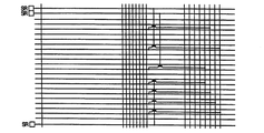
デマルチプレクサ256及びマルチプレクサ258の代わりに異なる経路付け回路を使用してJTAGテスト信号の別の経路付けを行うことも可能である。例えば、テスト信号は、インターフェース16におけるJTAGブロック254を介して、次いで、プログラム可能論理12の周辺部周り又はチップ250全体の周りに経路付けさせることが可能である。
【0050】
図14Aは専用論理14とプログラム可能論理12との間の境界に沿ってのテストスキャンを使用した別の実施例を例示している。図14Aの実施例においては、一連のスキャンセル261乃至265が専用論理14とプログラム可能論理12との間の境界にある。スキャンセル261及び262はインターフェース16におけるバッファ100から信号を受取る。該信号はプログラム可能論理12における論理280を介して通過することが可能であるが、プログラム可能論理12において支配的に使用されるクロック信号PCLKと同期される。クロックツリー294を介して信号PCLKを受取るフリップフロップ290及び292は該信号の同期を例示している。通常動作モード期間中、スキャンセル261及び262はバッファ100からの信号を専用論理14における論理260へ通過させる。テストモードにおけるこれらスキャンセルの動作については図15を参照して以下に説明する。
【0051】
プログラム可能論理12からのクロック信号PCLKはバッファ100を介して専用論理14へ通過し、且つクロックツリー272が信号PCLKに対する同期を必要とする信号に対して専用論理14を介してクロック信号PCLKを分布させる。このような1つの信号はフリップフロップ271からのものである。スキャンセル263がその信号を受取り、且つ通常動作期間中、その信号をインターフェース16におけるバッファ110へ通過させる。そこから、該信号はプログラム可能論理12における論理280へ入る。
【0052】
専用論理14はクロックツリー276を介して分布されたクロック信号DCLKを支配的に使用する。例示したように、専用論理14における論理273はフリップフロップ274が信号DCLKと同期させる信号を発生することが可能である。通常動作期間中、スキャンセル265はフリップフロップ274からの信号をインターフェース16内のバッファ110へ通過させ、且つバッファ110はその信号をプログラム可能論理12内の論理286へ通過させる。
【0053】
クロック信号DCLKは、又、信号PCLKとの同期を必要とする信号に対して、バッファ110を介しプログラム可能論理12へ通過させることが可能である。図14Aにおいてフリップフロップ296は、論理284及びバッファ100を介してスキャンセル264へ通過する信号PCLKと同期した信号を発生する。
【0054】
図14Bはスキャンセル261の例示的実施例を示している。スキャンセル261は入力マルチプレクサ266、フリップフロップ267及び268、出力マルチプレクサ269を有している。テスト期間中、初期的に、入力マルチプレクサ266が論理280に依存する値を有する入力信号PIを選択する。フリップフロップ267がスキャンクロック信号SCLKに応答してマルチプレクサ266からの出力信号をレジスタし且つその値をスキャン出力信号SOに対して出力する。フリップフロップ268はクロック信号UCLKに応答して信号SOの値をレジスタし且つその値をマルチプレクサ269へ出力する。マルチプレクサはテスト期間中フリップフロップ268からの信号を選択する。テストの場合には、ICに対する入力信号の全てが既知であり従って信号PIに対する適切な値は既知である。信号PIの値は初期的にフリップフロップ267及び268内に記録される。
【0055】
スキャンセル261乃至267は互いに接続されており、従って1個のスキャンセルからのスキャン出力信号SOは次のスキャンセルに対するスキャン入力信号SIである。フリップフロップ267におけるスキャン値を読み出すために、スキャンクロック信号がトグルされ、従って一方のスキャンセルにおけるレジスタ267からの値が次のセル内のレジスタ267内に記録される。クロック信号UCLKはこの時間期間中トグル動作されることはなく、従ってフリップフロップ268及びマルチプレクサ269からの出力は一定状態に止まる。スキャンセルの最後のものからの出力はI/Oパッドへ接続させることが可能であり、従ってスキャンセルからの二進値はスキャンクロックの周波数において1つづつ検査することが可能である。
【0056】
通常動作期間中、出力マルチプレクサ269は入力信号PIを受取り且つ出力信号として選択する。従って、入力信号PIは非常に僅かな遅延でもってスキャンセル261を介して通過する。
【0057】
図15Aは集積回路10及びパワー経路付け構造300におけるプログラム可能論理12及び専用論理14の概略図を示している。図15Aから理解されるように、プログラム可能論理12及び専用論理14用の経路付け構造は必ずしも同一の幅即ちピッチを有するものではない。特に、プログラム可能論理12に対するI/Oバッファ及び回路は専用論理14に対するI/Oバッファ及び回路とは異なる場合がある。インターフェースにおけるパワーバス302がパワー経路付け構造を一体的に結合している。
【0058】
図15Bはパワーバス302のより詳細な図を示している。図15Bから理解されるように、プログラム可能論理12の側に多数の導体が存在しており、且つ異なる数の導体が専用デバイス14の側に存在している。1例として、プログラム可能論理12上の導体304,305,306,307は、夫々、接地、3V、第二接地、5Vである。専用論理14上の導体310,311,312,313,314,315は、夫々、接地、5V、第二接地、3V、第三接地、第二3Vである。パワーバス302はプログラム可能論理12の導体を専用論理14の適宜の導体と結合している。従って、例えば、パワーバスは導体304を導体312及び314の両方へ結合しており、導体305は導体311へ結合しており、導体306は導体313及び315へ結合しており、且つ導体307は導体310へ結合している。従って、プログラム可能論理12及び専用論理14の両方へパワーを供給するために単一の組の入力/出力端子を使用することが可能である。
【0059】
本発明の例示的な実施例においては、専用論理14がPCIインターフェース及び関連する回路ブロックを有しており、且つプログラム可能論理12がFPGAを有している。該例示的な実施例の1つの特定な例はクイックロジック、インコーポレイテッドから直に入手可能なQL5064である。この特許出願の出願時においてクイックロジックから入手可能なQL5064予備的データシート及びQL5064ユーザーズマニアル、改定0.98は、QL5064について記載しておりその全体を引用によって本明細書に取込む。この実施例においては、プログラム可能論理12はユーザがユーザの回路に対して必要に応じてプログラムすることが可能な柔軟性のあるバックエンドインターフェースを提供する。従って、ユーザは、ユーザのデバイスにとって必ずしも最適なものでない例えばパワーPCインターフェース等の固定されたインターフェースを使用することに制限されるものではない。然しながら、該専用回路はPCIインターフェースを形成する一般的であるが複雑な機能を実現し、PCIインターフェースを形成せんとする負担をユーザから解放する。
【0060】
図16は本発明の例示的実施例に基づく集積回路410を包含するシステムのブロック図である。この例示的実施例においては、専用論理はPCIコア414であり、且つプログラム可能論理はFPGAである。図16のシステムは、ホストコンピュータのPCIバス35へ取付けられるデバイスである。IC410のPCIコア414がPCIバス350へ結合し、且つFPGA412はユーザ回路420へ結合する。例示的な適用例においては、IC410及びユーザ回路420はホストコンピュータのPCIバス350と電気的に接続するためにホストコンピュータにおけるスロット内にプラグインされるプリント回路基板上に装着されている。PCIコア414はPCIホスト制御器としても作用する。ユーザ回路420は、例えば、ビデオ、サウンド、通信又は処理等の所望の機能を実現することが可能であり、且つFPGA412は殆どの8ビット乃至64ビットマイクロプロセッサに対して接着剤のないインターフェースを提供することが可能である。
【0061】
PCIコア414はPCIバス350へ接続するPCIインターフェースバッファ及び論理352を有している。より詳細には、バッファ及び論理352はPCI標準が定義する信号の受取り及び送信のためにIC410のI/Oピンへ結合する。PCIプロトコルを実現するために、PCIコア414は、更に、ターゲット制御器354及びマスター制御器358を有している。インタラプト制御器404がPCIバス350上のインタラプト信号を制御し、且つ通信ブロック406がバッファを必要とすることのないPCI通信を実現する。特に、通信ブロック406は単一のデータから最大で64ビットの長さのものを転送するためのメールボックスレジスタ、及びPCIデバイスの通信用のI2O標準を実現するための回路を有している。PROM18からのコンフィギュレーションデータを使用するコンフィギュレーションブロック402はPCIコア414のコンフィギュレーションパラメータを決定する。
【0062】
5個のDMA制御器360は、メインメモリ又はPCIバス350上のデバイスからFIFOバッファ362,363,364へ及びFIFOバッファ366,367,368からメインメモリ又はPCIバス350上のデバイスへのデータを転送する直接メモリアクセス動作を制御する。例示的な実施例においては、各バッファ362乃至364及び366乃至368は少なくとも72ビット幅であり、データに対する64ビットとバイトイネーブルに対する8ビットとを包含している。FIFOバッファ362は「ターゲット書込バッファ」又はポストフェッチバッファであり且つ約32クワッドワードの深さである。FIFOバッファ363及び364はマスター受信バッファであり且つ持続バースト転送をサポートするために約64クワッドワードの深さである。FIFOバッファ366は「ターゲット読取バッファ」又はプレフェッチバッファであり、且つ約16クワッドワードの深さである。FIFOバッファ367及び368はマスター送信バッファであり且つ持続バースト転送をサポートするために約64クワッドワードの深さである。
【0063】
FIFOバッファ362,363,364からのデータは一方向バス370及び二方向バス390を介してFPGA412内へ流れる。FPGA412からのデータは一方向バス370及び二方向バス390を介してFIFOバッファ366,367,368内へ流れる。レーン操縦回路374がFIFOバッファ362乃至364とバス370との間にある。レーン操縦回路374が受取った64ビットデータを任意のバイトと整合させることを可能とするバレルシフタを有している。同様に、レーン操縦回路384及びデータ構成ユニット382がバス380とFIFOバッファ366乃至368との間にある。レーン操縦回路384はFPGA412からの64ビットデータを再整合させることが可能であり、且つデータ構成ユニット382はFPGA412からの2つの連続したデータ値からのバイトを使用して64ビットの整合されたデータを構成することが可能である。双方向バス390はFIFOバッファ362乃至364からか又はバッファ及び論理352からのいずれかからのデータ転送を選択する制御インターフェース395を有している。
【0064】
バッファ及びインターフェース352はPCIバス350を介しての同期通信のためのバスクロック信号PCI CLK (典型的に66MHzの周波数)を受取る。PCIコア414が同期的データ転送のためにクロック信号PCI CLKを使用し且つインターフェース46を介してFPGA412へクロック信号PCI CLKを通過させる。
【0065】
FPGA412は別のユーザクロック信号USER CLKも有しており、それはユーザ回路420へのデータ転送のためであるが、典型的に、クロック信号PCI CLKと同期されているものではない。FIFOバッファ362乃至364及び366乃至368はIC410におけるクロックドメインを横断してのデータ転送を可能とする。例示的実施例においては、クロック信号USER CLKは最大で100MHzの周波数を有することが可能である。然しながら、PCIデバイスは、しばしば、PCIバス用のクロック周波数よりも低いクロック信号を使用する。クロック信号USER CLKの周波数がクロック信号PCI CLKの周波数よりも低い場合には、IC410はPCIコア414とFPGA412との間を走行する複数個の64ビットバスを有しているので、IC410はPCIコア412とFPGA414との間での転送において完全なるPCIデータ帯域幅を使用することが可能である。特に、図10に示したような3個のバスの場合には、クロック信号USER CLKは22MHz程度に低い周波数を有することが可能であり且つ66MHzのPCIバス350の全データ帯域幅を使用することが可能である。更に、同一のIC410上にPCIコア414及びFPGA412を組込むことは、PCIコア414及びFPGA414が別々のICデバイスであった場合に必要とされるであろうような各データラインに対して1個のI/Oピンを有することのない多数のデータラインとすることを可能とする。
【0066】
図16のIC410のような集積回路の設計は、一般的に、回路コンポーネントの遅延及びタイミングを決定するためのシミュレーションを必要とする。特に、同期回路は、クロック動作されるレジスタ又はラッチ間の回路が1つのクロックサイクル内において所要の論理動作を完了するのに充分に高速であることを必要とする。IC410のような回路は現在入手可能な回路シミュレーションソフトウエアに対してチャンレンジを提示している。何故ならば、FPGA412において実現される配線及び実際の論理はユーザがFPGA412をプログラムするまで未知だからである。このことは専用論理412のシミュレーションを困難なものとする。何故ならば、専用論理412はFPGA412から信号を受取り且つそれへ信号を送るからである。
【0067】
1つのシミュレーション方法は、専用論理412のシミュレーションに対するパラメータとしてFPGA412からのドライバ強度を単純に使用する。然しながら、このことが行われると、現在のシミュレーションソフトウエアはインターフェース16におけるドライバと専用論理12における第一論理要素との間の導電性相互接続長さを無視する。IC製造技術がより小型の寸法を達成するに従い、専用論理12の実際のシミュレーションに対して相互接続長さの影響が重要なものとなる。特に、0.35ミクロン以下の相互接続体の場合には、該相互接続体は顕著な遅延となる。
【0068】
本発明の1つの側面によれば、FPGA412に対する簡単なモデルは、PCIコア16をシミュレーションする場合に、例えばシノプシスデザインコンパイラー等の現在のシミュレーションソフトウエアが適切にFPGA412を考慮することを可能とする。図17は専用論理12と共に使用するためのプログラム可能論理用のモデル422の1実施例を示している。プログラム可能論理のモデル422はバッファ110へ結合されているI/O (入力)パッド431及びバッファ100へ結合されているI/Oパッド (出力)100を有している。バッファ100及び110は使用されるべき実際の駆動強度に従って正確にモデル化される。シミュレーションにおいては、パッドはピン容量及びそのモデルにおけるスリュー対容量テーブルを有している。このシミュレーションは、プログラミング前においては予測不可能なものであるプログラム可能論理において使用される実際の回路及びバッファとパッドとの間のリード長を無視することが可能である。然しながら、従来のソフトウエアはバッファ100及び110と専用論理12との間の相互接続長を正確に考慮する。
【0069】
単に2個のパッドを使用することはプログラム可能論理に対するモデルを簡単化するが、所望により、付加的なパッドを付加し且つ選択したバッファへ接続することが可能である。例えば、入力クロック信号に対するパッド、又はPROMバッファに対するパッド等である。
【0070】
本発明を例示的な目的のためにある特定の実施例に関連して説明したが、本発明はそれらに制限されるものではない。種々の図面における種々の構成の表示は例示的なものである。本発明の側面はアモルファスシリコンアンチヒューズ及び酸化物−窒化物−酸化物アンチヒューズに制限されるべきものではなく、その他のアンチヒューズ構造へ拡張される。更に、理解すべきことであるが、導電性経路付け資源は任意の適宜の導電性物質又は物質の組合わせによって構成することが可能であり金属から構成されることが必要なものではない。従って、説明した実施例の種々の特徴の種々の修正、適用及び組合わせは特許請求の範囲に定義した発明の範囲から逸脱することなしに実施することが可能である。
【図面の簡単な説明】
【図1】 プログラム可能論理と、専用デバイスと、それらの間のインターフェースとを有する本発明の1実施例に基づく集積回路の概略図。
【図2】 アンチヒューズを使用したインターフェースの一部及びプログラム可能論理の1実施例の1つの大きな概略図を形成するためにどのようにして図2A,2B1,2B2,2B3,2C,2D,2E,2F1,2F2,2F3,2G,2H,2I,2J1,2J2,2J3,2K,2L,2M,2N1,2N2,2N3,2O,2P,2Q,2R1,2R2,2R3,2S,2Tを合成するかを示した概略図。
【図2A】 図2に示した概略図の一部を構成する部分的概略図。
【図2B1】 図2に示した概略図の一部を構成する部分的概略図。
【図2B2】 図2に示した概略図の一部を構成する部分的概略図。
【図2B3】 図2に示した概略図の一部を構成する部分的概略図。
【図2C】 図2に示した概略図の一部を構成する部分的概略図。
【図2D】 図2に示した概略図の一部を構成する部分的概略図。
【図2E】 図2に示した概略図の一部を構成する部分的概略図。
【図2F1】 図2に示した概略図の一部を構成する部分的概略図。
【図2F2】 図2に示した概略図の一部を構成する部分的概略図。
【図2F3】 図2に示した概略図の一部を構成する部分的概略図。
【図2G】 図2に示した概略図の一部を構成する部分的概略図。
【図2H】 図2に示した概略図の一部を構成する部分的概略図。
【図2I】 図2に示した概略図の一部を構成する部分的概略図。
【図2J1】 図2に示した概略図の一部を構成する部分的概略図。
【図2J2】 図2に示した概略図の一部を構成する部分的概略図。
【図2J3】 図2に示した概略図の一部を構成する部分的概略図。
【図2K】 図2に示した概略図の一部を構成する部分的概略図。
【図2L】 図2に示した概略図の一部を構成する部分的概略図。
【図2M】 図2に示した概略図の一部を構成する部分的概略図。
【図2N1】 図2に示した概略図の一部を構成する部分的概略図。
【図2N2】 図2に示した概略図の一部を構成する部分的概略図。
【図2N3】 図2に示した概略図の一部を構成する部分的概略図。
【図2O】 図2に示した概略図の一部を構成する部分的概略図。
【図2P】 図2に示した概略図の一部を構成する部分的概略図。
【図2Q】 図2に示した概略図の一部を構成する部分的概略図。
【図2R1】 図2に示した概略図の一部を構成する部分的概略図。
【図2R2】 図2に示した概略図の一部を構成する部分的概略図。
【図2R3】 図2に示した概略図の一部を構成する部分的概略図。
【図2S】 図2に示した概略図の一部を構成する部分的概略図。
【図2T】 図2に示した概略図の一部を構成する部分的概略図。
【図3】 本発明の別の実施例に基づく集積回路の概略図。
【図4】 図1に示した埋込型回路におけるプログラム可能論理用のプラットフォームとして使用することが可能な一部を有するフィールドプログラマブルゲートアレイ (FPGA)の簡単化した概略図。
【図5】 専用デバイスとプログラム可能論理における複数個のマクロセルとの間のインターフェースを示した概略図。
【図6】 プログラム可能論理と専用デバイスとの間のクロックインターフェースを示した概略図。
【図7】 2個のインターフェースバッファとテスト回路とを示した概略図。
【図8】 プログラム可能論理と専用デバイスとの間のインターフェースバッファ及びテスト回路及び専用デバイスとプログラム可能論理との間のインターフェースバッファ及びテスト回路を示した概略図。
【図9】 PROMと専用デバイスとの間のインターフェースバッファ及びテスト回路を示した概略図。
【図10】 テスト用トランジスタへ結合されており且つテスト回路内の弱検知回路の概略図。
【図11】 インターフェースバッファのうちの1個のセルと関連するテスト構成の相互接続を示した概略図。
【図12】 本発明の1実施例に基づくJTAG回路の概略図。
【図13】 本発明において使用することが可能であり且つIEEE標準に基づくJTAGレジスタの従来のコンフィギュレーション (形態特定)を示した概略図。
【図14A】 専用論理とプログラム可能論理との間の境界におけるテスト用のスキャンセルの使用を示した概略図。
【図14B】 専用論理とプログラム可能論理との間の境界におけるテスト用のスキャンセルの使用を示した概略図。
【図15A】 本発明の1実施例に基づく電源経路付け構成を示した概略図。
【図15B】 本発明の1実施例に基づく電源経路付け構成を示した概略図。
【図16】 専用デバイスがPCIバスへのインターフェースを実現する本発明の1実施例を示した概略ブロック図。[0001]
BACKGROUND OF THE INVENTION
The present invention relates to an integrated circuit having programmable logic such as a field programmable gate array, dedicated logic such as an ASIC type device, and an interface for communication between the programmable device and the dedicated device.
[0002]
[Prior art]
The semiconductor industry is driven by a desire to provide a higher level of integration. For higher levels of integration, silicon space and cost are reduced while performance and reliability are increased. However, higher levels of integration lead to greater specificity. For example, application specific integrated circuits (ASICs) are often highly specific devices that merely serve the needs of a single customer.
[0003]
Programmable logic devices such as field programmable gate arrays (FPGAs) are a variety of integrated circuit chips that can be selected by the user that can be configured by the user to implement specific functions for the user. It has internal circuit logic with a connected state. Programmable logic is diverse, but significant design challenges in terms of size, routing, and pinout stability when mapping large and complex functions onto a silicon platform containing programmable logic Is present.
[0004]
Programmable logic devices can be linked with separate dedicated devices, but there are on / off-chip delays associated with them, large board area, and high cost. Furthermore, it is possible to program the programmable logic to perform the desired function, but this is an expensive proposal and the resulting performance is often unacceptable.
[0005]
[Problems to be solved by the invention]
Therefore, there is a need for a single integrated device that combines the flexibility of programmable logic with the performance and reliability of dedicated devices.
[0006]
[Means for Solving the Problems]
Programmable logic such as a field programmable gate array and a dedicated device such as an ASIC type device are integrally coupled on a single integrated circuit with an antifuse-based interface. Configurable non-volatile memory using programmable logic techniques provides parameter settings for a dedicated device or its convenient on-chip configuration. In one embodiment, the platform for programmable logic is half of existing programmable logic devices, which advantageously eliminates the need to configure programmable logic. Dedicated devices can implement complex but often required functions, such as bus interfaces to industry standard buses, while programmable circuitry allows the user to implement custom functions. Placing both dedicated devices and programmable logic on the same chip allows for high processing power between circuits, but the communication is internal to the integrated circuit chip, so there are more I / O pins are not required.
[0007]
Programmable logic can include a clock network that receives clock signals from input / output terminals as well as from a clock network within a dedicated device. Thus, the programmable logic can operate at a frequency independent of the dedicated circuit. The input / output clock terminals for programmable logic are usually on one side of the chip closest to the programmable logic, while the input / output clock terminals for dedicated devices are on the opposite side of the chip closest to the dedicated devices. It's above. The clock network distributes the clock signal to both programmable logic and dedicated devices.
[0008]
The interface between the dedicated device and the programmable logic has a number of conductors with buffers and test circuitry. The test circuit includes a PMOS test transistor and an NMOS test transistor, the gates of which are coupled to the output terminal of the buffer. The PMOS test transistor is coupled between the voltage supply and the output terminal, while the NMOS test transistor is coupled between the ground supply and the different output terminal. The output terminal of the PMOS test transistor is coupled to the output terminal of the inverter. During the test mode, the inverter is coupled to a voltage supply. The PMOS test transistor is much larger than the NMOS transistor in the inverter. Thus, when the PMOS test transistor is off, the inverter drives the output terminal low, but when the PMOS test transistor is on, the PMOS test transistor drives the output terminal high. . The output terminal of the NMOS test transistor is coupled to the output terminal of another inverter that is coupled to the ground source during the test operation. The NMOS test transistor is much larger than the PMOS transistor in the inverter. The test circuit allows the buffer to be beneficially tested without programming an antifuse coupled to the conductor.
[0009]
According to another embodiment of the present invention, the input / output terminals at and around the interface between the programmable logic and the dedicated device are tested using JTAG registers. The path of the test signal through the JTAG register can be selected to pass around the periphery of both the programmable logic and the dedicated device, or through the interface and around the periphery of the dedicated device.
[0010]
DETAILED DESCRIPTION OF THE INVENTION
FIG. 1 is a schematic diagram of an integrated
[0011]
FIG. 1 further shows a programmable read only memory (PROM) 18. PROM 18 stores data that configures or sets parameters for
[0012]
Beneficially, the integrated
[0013]
FIG. 2 shows how to form one large simplified schematic of one embodiment of
[0014]
FIG. 2 shows the two configurations of FIG. 2B disposed between the configurations of FIGS. 2A and 2C, and the two configurations of FIG. 2B are between the configurations of FIGS. 2C and 2D in the composite diagram. Arranged and the configuration of FIG. 2B is 3 to make the
[0015]
The operation of the programmable logic as shown in FIGS. 2A-2T is described in US Pat. No. 5, entitled “Programmable Architecture for a Programmable Integrated Circuits Integrating Antifuses”. No. 825,201, which is incorporated herein by reference.
[0016]
FIGS. 2Q-2T show the portion of
[0017]
FIG. 2R1 shows a portion of the
[0018]
Also shown in FIG. 2R1 is
[0019]
The
[0020]
FIG. 3 is a schematic diagram of an
[0021]
Although the
[0022]
FIG. 4 is a simplified schematic diagram of a field programmable gate array (FPGA) 50. As shown in FIG. 4, the
[0023]
To generate the integrated circuit 10 (FIG. 1), the halved
[0024]
FIG. 5 shows an interface between a plurality of
[0025]
FIG. 6 is a schematic diagram of a
[0026]
Pad 86 receives a clock signal DCLK that drives
[0027]
In accordance with another aspect of the present invention, the
[0028]
A select signal to the multiplexers 103 [0] to 103 [n-1] controls whether the buffers 100 [0] to 100 [n-1] operate in the normal mode or the test mode. In the normal mode, the select signals are the multiplexers 103 [0] to 103 [n-1] and the enable signals EN [0] to EN [n-1] are sent to the NAND gates 102 [0] to 102 [n-1]. To each of the second input terminals. Each of enable signals EN [0] to EN [n-1] is high (to disable) a corresponding one of buffers 100 [0] to 100 [n-1] during normal mode operation. Low).
[0029]
In the test mode, the select signal passes through the multiplexers 103 [0] to 103 [n-1] and is output from the registers 105 [0] to 105 [n-1], respectively. n−1] is applied to the second input terminals of the NAND gates 102 [0] to 102 [n−1]. The registers 105 [0] to 105 [n-1] are connected in a chain, and i is 0 to n-2, and the output terminal of the register 105 [i] is connected to the input terminal of the register 105 [i + 1]. ing. The clock signal Clk controls the latching of the value of the input test signal Tin into the register 105 [0] and the propagation of the value through the register chain 105 [0] to 105 [n-1].
[0030]
The
[0031]
In order to test the buffers 100 [0] to 100 [n-1], the select signal Sel causes the multiplexers 103 [0] to 103 [n-1] to generate the signals T [0] to T [n-1]. Route to NAND 102 [0] through 102 [n-1]. The signals PLout [0] to PLout [n−1] to the other input terminals of the NAND gates 102 [0] to 102 [n−1] are high from the unprogrammable
[0032]
[0033]
If signal TIn is raised high for a single clock cycle while all of signals T [0] through T [n-1] are low, then from register 105 [0] to 105 [n-1]. Start a high voltage state propagating via signals T [0] to T [n-1]. A high signal T [i] turns off the corresponding transistor 106 [i] and turns on the corresponding transistor 108 [i]. Accordingly, at least one of the transistors 108 [0] to 108 [n-1] should be on during the entire time that the high state is propagating through the registers 105 [0] to 105 [n-1]. As such, the test output signal TOUT2 should remain high. If the test output signal falls low during any clock cycle i after raising signal TIn, buffer 100 [i] has failed and signal T [i] is high. The output signal DLin [i] is not raised to a high state. The buffer causing this malfunction can be identified from the time when the state of the signal TOUT2 changes.
[0034]
A similar test pattern for signal TIn can raise all of signals T [0] to T [n-1] to a high state and drop the voltage state of signal TIn to a low for one clock cycle. Is possible. It is also possible to use the test pattern. In this way, it is possible to identify individual defective buffers. The described test allows to effectively test the interface buffers 100 [0] to 100 [n-1] without programming programmable elements of programmable logic.
[0035]
A test circuit similar to that shown in FIG. 7 can also be used to test buffers that carry signals from dedicated logic to programmable logic. In addition, two types of buffers can be connected in the same scan chain or in separate scan chains for testing purposes. FIG. 8 illustrates an
[0036]
The
[0037]
FIG. 9 shows an
[0038]
FIG. 10 is a schematic diagram of a
[0039]
The signals gcnr and gcnd are test signals similar to the signals inn and inp from other test buses (not shown).
[0040]
FIG. 11 is a schematic diagram illustrating the interconnection of
[0041]
In each interface cell 130 [i], the data register 105 [i] supplies the test data signal T [i] to the interface buffer in the
[0042]
Since the register in each cell provides a test signal T [i] and the test bus signal is from a test transistor, it is not necessary to program the
[0043]
FIG. 12 is a schematic diagram of an
[0044]
FIG. 13 shows a configuration for a JTAG register that conforms to the IEEE standard and is suitable for JTAG block 252 or 254. Each JTAG block is associated with a
[0045]
As shown in FIG. 12, the
[0046]
[0047]
To test I / O on the periphery of
[0048]
On the other hand, in the case of a JTAG test around
[0049]
It is also possible to use another routing circuit in place of the
[0050]
FIG. 14A illustrates another embodiment using a test scan along the boundary between
[0051]
The clock signal PCLK from the
[0052]
[0053]
The clock signal DCLK can also be passed through the
[0054]
FIG. 14B shows an exemplary embodiment of the
[0055]
Since the
[0056]
During normal operation,
[0057]
FIG. 15A shows a schematic diagram of
[0058]
FIG. 15B shows a more detailed view of the
[0059]
In an exemplary embodiment of the invention,
[0060]
FIG. 16 is a block diagram of a system including an
[0061]
The
[0062]
Five
[0063]
Data from the FIFO buffers 362, 363, 364 flows into the
[0064]
The buffer and
[0065]
The
[0066]
The design of an integrated circuit, such as
[0067]
One simulation method simply uses the driver strength from the
[0068]
In accordance with one aspect of the present invention, a simple model for
[0069]
Using only two pads simplifies the model for programmable logic, but additional pads can be added and connected to selected buffers as desired. For example, a pad for an input clock signal or a pad for a PROM buffer.
[0070]
Although the invention has been described in connection with certain specific embodiments for illustrative purposes, the invention is not limited thereto. The representation of the various configurations in the various drawings is exemplary. Aspects of the present invention should not be limited to amorphous silicon antifuses and oxide-nitride-oxide antifuses, but extend to other antifuse structures. Further, it should be understood that the conductive routing resource can be composed of any suitable conductive material or combination of materials and need not be composed of metal. Accordingly, various modifications, applications and combinations of the various features of the described embodiments can be practiced without departing from the scope of the invention as defined in the claims.
[Brief description of the drawings]
FIG. 1 is a schematic diagram of an integrated circuit according to one embodiment of the present invention having programmable logic, dedicated devices, and an interface therebetween.
FIG. 2 shows how to form a large schematic diagram of one embodiment of a portion of an interface and programmable logic using antifuses, FIG. 2A, 2B1, 2B2, 2B3, 2C, 2D, 2E , 2F1, 2F2, 2F3, 2G, 2H, 2I, 2J1, 2J2, 2J3, 2K, 2L, 2M, 2N1, 2N2, 2N3, 2O, 2P, 2Q, 2R1, 2R2, 2R3, 2S, 2T FIG.
2A is a partial schematic diagram constituting a part of the schematic diagram shown in FIG. 2. FIG.
2B1 is a partial schematic diagram constituting a part of the schematic diagram shown in FIG. 2. FIG.
2B2 is a partial schematic diagram constituting a part of the schematic diagram shown in FIG. 2. FIG.
2B3 is a partial schematic diagram that forms part of the schematic diagram shown in FIG. 2. FIG.
FIG. 2C is a partial schematic diagram that forms part of the schematic diagram shown in FIG. 2;
FIG. 2D is a partial schematic diagram that forms part of the schematic diagram shown in FIG. 2;
2E is a partial schematic diagram that forms part of the schematic diagram shown in FIG. 2. FIG.
FIG. 2F1 is a partial schematic diagram constituting a part of the schematic diagram shown in FIG. 2;
FIG. 2F2 is a partial schematic diagram constituting a part of the schematic diagram shown in FIG.
FIG. 2F3 is a partial schematic diagram constituting a part of the schematic diagram shown in FIG.
FIG. 2G is a partial schematic diagram constituting a part of the schematic diagram shown in FIG.
FIG. 2H is a partial schematic diagram that forms part of the schematic diagram shown in FIG. 2;
FIG. 2I is a partial schematic diagram that forms part of the schematic diagram shown in FIG. 2;
2J1 is a partial schematic diagram constituting a part of the schematic diagram shown in FIG. 2. FIG.
FIG. 2J2 is a partial schematic diagram constituting a part of the schematic diagram shown in FIG.
FIG. 2J3 is a partial schematic diagram constituting a part of the schematic diagram shown in FIG.
FIG. 2K is a partial schematic diagram constituting a part of the schematic diagram shown in FIG.
FIG. 2L is a partial schematic diagram that forms part of the schematic diagram shown in FIG. 2;
FIG. 2M is a partial schematic diagram that forms part of the schematic diagram shown in FIG. 2;
FIG. 2N1 is a partial schematic diagram constituting a part of the schematic diagram shown in FIG. 2;
2N2 is a partial schematic diagram that forms part of the schematic diagram shown in FIG. 2;
FIG. 2N3 is a partial schematic diagram that forms part of the schematic diagram shown in FIG.
FIG. 2O is a partial schematic diagram that forms part of the schematic diagram shown in FIG. 2;
FIG. 2P is a partial schematic diagram that forms part of the schematic diagram shown in FIG. 2;
FIG. 2Q is a partial schematic diagram constituting a part of the schematic diagram shown in FIG. 2;
FIG. 2R1 is a partial schematic diagram constituting a part of the schematic diagram shown in FIG.
FIG. 2R2 is a partial schematic diagram constituting a part of the schematic diagram shown in FIG.
FIG. 2R3 is a partial schematic diagram constituting a part of the schematic diagram shown in FIG.
FIG. 2S is a partial schematic diagram constituting a part of the schematic diagram shown in FIG. 2;
FIG. 2T is a partial schematic diagram that forms part of the schematic diagram shown in FIG. 2;
FIG. 3 is a schematic diagram of an integrated circuit according to another embodiment of the present invention.
4 is a simplified schematic diagram of a field programmable gate array (FPGA) having a portion that can be used as a platform for programmable logic in the embedded circuit shown in FIG. 1. FIG.
FIG. 5 is a schematic diagram illustrating an interface between a dedicated device and a plurality of macrocells in programmable logic.
FIG. 6 is a schematic diagram illustrating a clock interface between programmable logic and a dedicated device.
FIG. 7 is a schematic diagram showing two interface buffers and a test circuit.
FIG. 8 is a schematic diagram illustrating an interface buffer and test circuit between a programmable logic and a dedicated device and an interface buffer and test circuit between the dedicated device and the programmable logic.
FIG. 9 is a schematic diagram showing an interface buffer and a test circuit between a PROM and a dedicated device.
FIG. 10 is a schematic diagram of a weak detection circuit coupled to a test transistor and within the test circuit.
FIG. 11 is a schematic diagram illustrating interconnection of test configurations associated with one cell of an interface buffer.
FIG. 12 is a schematic diagram of a JTAG circuit according to one embodiment of the present invention.
FIG. 13 is a schematic diagram showing a conventional configuration (configuration specific) of a JTAG register that can be used in the present invention and is based on the IEEE standard.
14A is a schematic diagram illustrating the use of test scan cells at the boundary between dedicated logic and programmable logic. FIG.
FIG. 14B is a schematic diagram illustrating the use of a test scan cell at the boundary between dedicated logic and programmable logic.
FIG. 15A is a schematic diagram illustrating a power routing arrangement according to one embodiment of the present invention.
FIG. 15B is a schematic diagram illustrating a power routing arrangement according to one embodiment of the present invention.
FIG. 16 is a schematic block diagram showing an embodiment of the present invention in which a dedicated device implements an interface to a PCI bus.
Claims (13)
プログラム可能論理、
専用デバイス、
前記専用デバイスと前記プログラム可能論理との間に配置されており且つプログラム可能なアンチヒューズのアレイを有しているインターフェース、
前記プログラム可能論理内の第一クロック回路、
前記専用デバイス内の第二クロック回路、
を有しており、
クロック信号を受取る複数個のパッドが設けられており、前記パッドが複数個の経路付け資源によって前記第一クロック回路へ結合されており、前記プログラム可能論理が前記専用デバイスとは独立的な周波数において動作することが可能であるように前記複数個のパッドの内の少なくとも1つが前記第一クロック回路及び前記第二クロック回路へ結合されていることを特徴とする集積回路。 In integrated circuits,
Programmable logic,
Dedicated device,
An interface disposed between the dedicated device and the programmable logic and having an array of programmable antifuses ;
A first clock circuit in the programmable logic;
A second clock circuit in the dedicated device;
Have
A plurality of pads are provided for receiving a clock signal, the pads are coupled to the first clock circuit by a plurality of routing resources, and the programmable logic is at a frequency independent of the dedicated device. An integrated circuit, wherein at least one of the plurality of pads is coupled to the first clock circuit and the second clock circuit so as to be operable .
前記プログラム可能論理から前記専用デバイスへの複数個の第一導体、
前記専用デバイスから前記プログラム可能論理への複数個の第二導体、
前記第一導体及び前記第二導体へ結合されているバッファ、
各バッファへ結合されているテスト回路であって、
電圧源へ結合されている第一端子と、第一出力端子へ結合されている第二端子と、前記バッファの出力端子へ結合しているゲート端子とを具備しているPMOSテストトランジスタ、
接地供給源へ結合している第一端子と、第二端子と、前記バッファの出力端子へ結合しているゲート端子とを具備しているNMOSテストトランジスタ、
を有しているテスト回路、
前記テスト回路へ結合している弱検知回路であって、
第一PMOSトランジスタと第一NMOSトランジスタとを包含している第一インバータであって、前記第一インバータが入力端子と出力端子とを具備しており、前記入力端子が電圧供給源へ結合しており、且つ前記出力端子が前記PMOSテストトランジスタの前記第二端子へ結合しており、前記PMOSテストトランジスタが前記第一インバータにおける前記第一NMOSトランジスタよりも大型である第一インバータ、
第二PMOSトランジスタと第二NMOSトランジスタとを包含している第二インバータであって、前記第二インバータが入力端子と出力端子とを具備しており、前記入力端子が接地供給源へ結合しており、且つ前記出力端子が前記NMOSテストトランジスタの前記第二端子へ結合しており、前記NMOSテストトランジスタが前記第二インバータにおける前記第一PMOSトランジスタよりも大型である第二インバータ、
を有している弱検知回路、
を有している集積回路。 The interface of claim 1 , further comprising:
A plurality of first conductors from the programmable logic to the dedicated device;
A plurality of second conductors from the dedicated device to the programmable logic;
A buffer coupled to the first conductor and the second conductor;
A test circuit coupled to each buffer,
A PMOS test transistor comprising a first terminal coupled to a voltage source, a second terminal coupled to a first output terminal, and a gate terminal coupled to the output terminal of the buffer;
An NMOS test transistor comprising a first terminal coupled to a ground source, a second terminal, and a gate terminal coupled to the output terminal of the buffer;
Having a test circuit,
A weak detection circuit coupled to the test circuit,
A first inverter including a first PMOS transistor and a first NMOS transistor, the first inverter having an input terminal and an output terminal, the input terminal being coupled to a voltage supply source; A first inverter having an output terminal coupled to the second terminal of the PMOS test transistor, the PMOS test transistor being larger than the first NMOS transistor in the first inverter;
A second inverter including a second PMOS transistor and a second NMOS transistor, the second inverter having an input terminal and an output terminal, the input terminal being coupled to a ground source; A second inverter, wherein the output terminal is coupled to the second terminal of the NMOS test transistor, the NMOS test transistor being larger than the first PMOS transistor in the second inverter;
Weak detection circuit, having
An integrated circuit .
前記形態特定可能な非揮発性メモリから前記専用デバイスへの複数個の第三導体、
を有しており、前記バッファが前記第一導体、前記第二導体、第三導体へ結合されている集積回路。11. The device of claim 10, further comprising a formable non-volatile memory, the interface further comprising:
A plurality of third conductors from the formable non-volatile memory to the dedicated device;
The has the buffer is the first conductor, the second conductor is coupled to the third conductor integrated circuit.
前記第一側部の周辺部周りにおける第一組の周辺入力/出力端子、
前記第二側部の周辺部周りにおける第二組の周辺入力/出力端子、
前記プログラム可能論理と前記専用デバイスとの間の1組のインターフェース入力/出力端子、
前記第一組の周辺入力/出力端子へ結合している第一組のJTAGレジスタ、
前記第二組の周辺入力/出力端子へ結合している第二組のJTAGレジスタ、
前記インターフェース入力/出力端子へ結合している第三組のJTAGレジスタ、
テスト信号を受取る入力端子と、セレクト端子と、前記第一組のJTAGレジスタへ結合している第一出力端子と、前記第三組のJTAGレジスタへ結合している第二出力端子とを具備しているデマルチプレクサ、
セレクト端子と、前記第一組のJTAGレジスタへ結合している第一入力端子と、前記第三組のJTAGレジスタへ結合している第二入力端子と、前記第二組のJTAGレジスタへ結合している出力端子とを具備しているマルチプレクサ、
を有している集積回路。The integrated circuit of claim 1 , wherein the integrated circuit has a first side on one side of the interface and a second side on the opposite side of the interface;
A first set of peripheral input / output terminals around the periphery of the first side;
A second set of peripheral input / output terminals around the periphery of the second side;
A set of interface input / output terminals between the programmable logic and the dedicated device;
A first set of JTAG registers coupled to the first set of peripheral input / output terminals;
A second set of JTAG registers coupled to the second set of peripheral input / output terminals;
A third set of JTAG registers coupled to the interface input / output terminals;
An input terminal for receiving a test signal; a select terminal; a first output terminal coupled to the first set of JTAG registers; and a second output terminal coupled to the third set of JTAG registers. Demultiplexer,
A select terminal; a first input terminal coupled to the first set of JTAG registers; a second input terminal coupled to the third set of JTAG registers; and a second input terminal coupled to the second set of JTAG registers. A multiplexer having an output terminal,
An integrated circuit .
Applications Claiming Priority (5)
| Application Number | Priority Date | Filing Date | Title |
|---|---|---|---|
| US15167399P | 1999-08-31 | 1999-08-31 | |
| US60/151,673 | 1999-08-31 | ||
| US09/650,773 US6552410B1 (en) | 1999-08-31 | 2000-08-29 | Programmable antifuse interfacing a programmable logic and a dedicated device |
| US09/650,773 | 2000-08-29 | ||
| PCT/US2000/023961 WO2001017112A1 (en) | 1999-08-31 | 2000-08-30 | Integrated circuit including dedicated and programmable logic |
Publications (2)
| Publication Number | Publication Date |
|---|---|
| JP2003531509A JP2003531509A (en) | 2003-10-21 |
| JP4673533B2 true JP4673533B2 (en) | 2011-04-20 |
Family
ID=26848857
Family Applications (1)
| Application Number | Title | Priority Date | Filing Date |
|---|---|---|---|
| JP2001520946A Expired - Lifetime JP4673533B2 (en) | 1999-08-31 | 2000-08-30 | Integrated circuit with dedicated and programmable logic |
Country Status (7)
| Country | Link |
|---|---|
| US (1) | US6552410B1 (en) |
| EP (1) | EP1219031B1 (en) |
| JP (1) | JP4673533B2 (en) |
| KR (1) | KR20020041420A (en) |
| AU (1) | AU7096800A (en) |
| DE (1) | DE60033538D1 (en) |
| WO (1) | WO2001017112A1 (en) |
Families Citing this family (24)
| Publication number | Priority date | Publication date | Assignee | Title |
|---|---|---|---|---|
| US7024653B1 (en) * | 2000-10-30 | 2006-04-04 | Cypress Semiconductor Corporation | Architecture for efficient implementation of serial data communication functions on a programmable logic device (PLD) |
| JP3990567B2 (en) * | 2001-12-18 | 2007-10-17 | 大日本スクリーン製造株式会社 | Diaphragm valve, substrate processing unit and substrate processing apparatus |
| DE10221772A1 (en) * | 2002-05-15 | 2003-11-27 | Flowtec Ag | Field bus unit is used to provide input from a range of sensors and has a built in digital signal processing capacity with a facility for being programmable |
| US7480010B2 (en) * | 2002-09-04 | 2009-01-20 | Denace Enterprise Co., L.L.C. | Customizable ASIC with substantially non-customizable portion that supplies pixel data to a mask-programmable portion in multiple color space formats |
| US7202908B2 (en) * | 2002-09-04 | 2007-04-10 | Darien K. Wallace | Deinterlacer using both low angle and high angle spatial interpolation |
| US7782398B2 (en) * | 2002-09-04 | 2010-08-24 | Chan Thomas M | Display processor integrated circuit with on-chip programmable logic for implementing custom enhancement functions |
| US7043703B2 (en) * | 2002-09-11 | 2006-05-09 | Lsi Logic Corporation | Architecture and/or method for using input/output affinity region for flexible use of hard macro I/O buffers |
| US6966044B2 (en) * | 2002-12-09 | 2005-11-15 | Lsi Logic Corporation | Method for composing memory on programmable platform devices to meet varied memory requirements with a fixed set of resources |
| US7069523B2 (en) * | 2002-12-13 | 2006-06-27 | Lsi Logic Corporation | Automated selection and placement of memory during design of an integrated circuit |
| US7020852B2 (en) * | 2003-05-08 | 2006-03-28 | Lsi Logic Corporation | Automation of the development, testing, and release of a flow framework and methodology to design integrated circuits |
| US6910201B2 (en) * | 2003-09-17 | 2005-06-21 | Lsi Logic Corporation | Custom clock interconnects on a standardized silicon platform |
| US7657689B1 (en) * | 2003-10-07 | 2010-02-02 | Altera Corporation | Methods and apparatus for handling reset events in a bus bridge |
| US7446562B2 (en) * | 2004-06-15 | 2008-11-04 | Nec Corporation | Programmable semiconductor device |
| US7117472B2 (en) * | 2004-07-09 | 2006-10-03 | Lsi Logic Corporation | Placement of a clock signal supply network during design of integrated circuits |
| US7363526B1 (en) * | 2004-09-07 | 2008-04-22 | Altera Corporation | Method for transferring data across different clock domains with selectable delay |
| DE102006011706B4 (en) * | 2006-03-14 | 2011-04-07 | Qimonda Ag | Semiconductor device, as well as semiconductor device test method |
| US8018248B2 (en) * | 2006-09-21 | 2011-09-13 | Quicklogic Corporation | Adjustable interface buffer circuit between a programmable logic device and a dedicated device |
| US7482834B2 (en) * | 2006-10-19 | 2009-01-27 | Quicklogic Corporation | Programmable multiplexer |
| US8091001B2 (en) * | 2006-11-30 | 2012-01-03 | Quicklogic Corporation | FPGA programming structure for ATPG test coverage |
| JP4492702B2 (en) * | 2008-01-11 | 2010-06-30 | トヨタ自動車株式会社 | Anomaly detection device |
| GB2466821A (en) * | 2009-01-08 | 2010-07-14 | Advanced Risc Mach Ltd | An FPGA with an embedded bus and dedicated bus interface circuits |
| CN103534692B (en) | 2011-05-17 | 2016-10-19 | 阿尔特拉公司 | Hard logic in docking hybrid integrated device and the system and method for soft logic |
| US9136842B2 (en) * | 2013-06-07 | 2015-09-15 | Altera Corporation | Integrated circuit device with embedded programmable logic |
| US10693468B2 (en) * | 2017-06-28 | 2020-06-23 | Texas Instruments Incorporated | Integrated circuit and process for family of digital logic functions |
Citations (2)
| Publication number | Priority date | Publication date | Assignee | Title |
|---|---|---|---|---|
| US5892684A (en) * | 1994-05-20 | 1999-04-06 | Quicklogic Corporation | Programmable application specific integrated circuit employing antifuses and methods therefor |
| JP2000509948A (en) * | 1997-02-28 | 2000-08-02 | アクテル・コーポレイション | Integrated circuit device |
Family Cites Families (7)
| Publication number | Priority date | Publication date | Assignee | Title |
|---|---|---|---|---|
| US5477165A (en) | 1986-09-19 | 1995-12-19 | Actel Corporation | Programmable logic module and architecture for field programmable gate array device |
| US5416367A (en) | 1991-03-06 | 1995-05-16 | Quicklogic Corporation | Programmable application specific integrated circuit and logic cell therefor |
| US5237218A (en) | 1991-05-03 | 1993-08-17 | Lattice Semiconductor Corporation | Structure and method for multiplexing pins for in-system programming |
| US5687325A (en) | 1996-04-19 | 1997-11-11 | Chang; Web | Application specific field programmable gate array |
| US5825201A (en) | 1996-06-21 | 1998-10-20 | Quicklogic Corporation | Programming architecture for a programmable integrated circuit employing antifuses |
| US5898776A (en) | 1996-11-21 | 1999-04-27 | Quicklogic Corporation | Security antifuse that prevents readout of some but not other information from a programmed field programmable gate array |
| US6246258B1 (en) * | 1999-06-21 | 2001-06-12 | Xilinx, Inc. | Realizing analog-to-digital converter on a digital programmable integrated circuit |
-
2000
- 2000-08-29 US US09/650,773 patent/US6552410B1/en not_active Expired - Lifetime
- 2000-08-30 AU AU70968/00A patent/AU7096800A/en not_active Abandoned
- 2000-08-30 DE DE60033538T patent/DE60033538D1/en not_active Expired - Lifetime
- 2000-08-30 JP JP2001520946A patent/JP4673533B2/en not_active Expired - Lifetime
- 2000-08-30 WO PCT/US2000/023961 patent/WO2001017112A1/en active IP Right Grant
- 2000-08-30 EP EP00959692A patent/EP1219031B1/en not_active Expired - Lifetime
- 2000-08-30 KR KR1020027002747A patent/KR20020041420A/en not_active Application Discontinuation
Patent Citations (2)
| Publication number | Priority date | Publication date | Assignee | Title |
|---|---|---|---|---|
| US5892684A (en) * | 1994-05-20 | 1999-04-06 | Quicklogic Corporation | Programmable application specific integrated circuit employing antifuses and methods therefor |
| JP2000509948A (en) * | 1997-02-28 | 2000-08-02 | アクテル・コーポレイション | Integrated circuit device |
Also Published As
| Publication number | Publication date |
|---|---|
| EP1219031A1 (en) | 2002-07-03 |
| WO2001017112A1 (en) | 2001-03-08 |
| KR20020041420A (en) | 2002-06-01 |
| JP2003531509A (en) | 2003-10-21 |
| EP1219031B1 (en) | 2007-02-21 |
| US6552410B1 (en) | 2003-04-22 |
| AU7096800A (en) | 2001-03-26 |
| DE60033538D1 (en) | 2007-04-05 |
Similar Documents
| Publication | Publication Date | Title |
|---|---|---|
| JP4673533B2 (en) | Integrated circuit with dedicated and programmable logic | |
| US7587537B1 (en) | Serializer-deserializer circuits formed from input-output circuit registers | |
| US8677306B1 (en) | Microcontroller controlled or direct mode controlled network-fabric on a structured ASIC | |
| US6211697B1 (en) | Integrated circuit that includes a field-programmable gate array and a hard gate array having the same underlying structure | |
| US9024657B2 (en) | Architectural floorplan for a structured ASIC manufactured on a 28 NM CMOS process lithographic node or smaller | |
| KR100491662B1 (en) | Enhanced field programmable gate array | |
| US6229336B1 (en) | Programmable integrated circuit device with slew control and skew control | |
| US7224181B1 (en) | Clock distribution in a configurable IC | |
| US8269524B2 (en) | General purpose input/output pin mapping | |
| US20080180131A1 (en) | Configurable IC with Interconnect Circuits that also Perform Storage Operations | |
| US7642809B2 (en) | Die apparatus having configurable input/output and control method thereof | |
| US20060028241A1 (en) | Structured integrated circuit device | |
| US6466049B1 (en) | Clock enable control circuit for flip flops | |
| JP2008512850A (en) | Structured integrated circuit device | |
| US20050021749A1 (en) | Method and apparatus for communication within a programmable logic device using serial transceivers | |
| US7119573B2 (en) | Field-programmable gate array low voltage differential signaling driver utilizing two complimentary output buffers | |
| US7800404B2 (en) | Field programmable application specific integrated circuit with programmable logic array and method of designing and programming the programmable logic array | |
| JP4108374B2 (en) | Scan flip-flop circuit, scan flip-flop circuit array, and integrated circuit device | |
| JP2001274253A (en) | Fpga compatible gate array | |
| US7545166B2 (en) | Field-programmable gate array low voltage differential signaling driver utilizing two complimentary output buffers | |
| US6242941B1 (en) | Reducing I/O noise when leaving programming mode | |
| Smith | Intel's FLEXlogic FPGA architecture | |
| JPS6123243A (en) | Logical integrated circuit | |
| JP2001165999A (en) | Semiconductor integrated circuit and semiconductor integrated circuit device using the same | |
| JP2003512628A (en) | Apparatus and method for programmable parametric toggle testing of digital CMOS pads |
Legal Events
| Date | Code | Title | Description |
|---|---|---|---|
| A621 | Written request for application examination |
Free format text: JAPANESE INTERMEDIATE CODE: A621 Effective date: 20070823 |
|
| A977 | Report on retrieval |
Free format text: JAPANESE INTERMEDIATE CODE: A971007 Effective date: 20100716 |
|
| A131 | Notification of reasons for refusal |
Free format text: JAPANESE INTERMEDIATE CODE: A131 Effective date: 20100727 |
|
| A601 | Written request for extension of time |
Free format text: JAPANESE INTERMEDIATE CODE: A601 Effective date: 20101027 |
|
| A602 | Written permission of extension of time |
Free format text: JAPANESE INTERMEDIATE CODE: A602 Effective date: 20101104 |
|
| A521 | Written amendment |
Free format text: JAPANESE INTERMEDIATE CODE: A523 Effective date: 20101129 |
|
| TRDD | Decision of grant or rejection written | ||
| A01 | Written decision to grant a patent or to grant a registration (utility model) |
Free format text: JAPANESE INTERMEDIATE CODE: A01 Effective date: 20101221 |
|
| A01 | Written decision to grant a patent or to grant a registration (utility model) |
Free format text: JAPANESE INTERMEDIATE CODE: A01 |
|
| A61 | First payment of annual fees (during grant procedure) |
Free format text: JAPANESE INTERMEDIATE CODE: A61 Effective date: 20110121 |
|
| R150 | Certificate of patent or registration of utility model |
Ref document number: 4673533 Country of ref document: JP Free format text: JAPANESE INTERMEDIATE CODE: R150 Free format text: JAPANESE INTERMEDIATE CODE: R150 |
|
| FPAY | Renewal fee payment (event date is renewal date of database) |
Free format text: PAYMENT UNTIL: 20140128 Year of fee payment: 3 |
|
| R250 | Receipt of annual fees |
Free format text: JAPANESE INTERMEDIATE CODE: R250 |
|
| R250 | Receipt of annual fees |
Free format text: JAPANESE INTERMEDIATE CODE: R250 |
|
| R250 | Receipt of annual fees |
Free format text: JAPANESE INTERMEDIATE CODE: R250 |
|
| R250 | Receipt of annual fees |
Free format text: JAPANESE INTERMEDIATE CODE: R250 |
|
| R250 | Receipt of annual fees |
Free format text: JAPANESE INTERMEDIATE CODE: R250 |
|
| R250 | Receipt of annual fees |
Free format text: JAPANESE INTERMEDIATE CODE: R250 |
|
| R250 | Receipt of annual fees |
Free format text: JAPANESE INTERMEDIATE CODE: R250 |
|
| EXPY | Cancellation because of completion of term |