JP4666928B2 - Weighted SAW reflection grating using dithered acoustic reflector - Google Patents
Weighted SAW reflection grating using dithered acoustic reflector Download PDFInfo
- Publication number
- JP4666928B2 JP4666928B2 JP2004044640A JP2004044640A JP4666928B2 JP 4666928 B2 JP4666928 B2 JP 4666928B2 JP 2004044640 A JP2004044640 A JP 2004044640A JP 2004044640 A JP2004044640 A JP 2004044640A JP 4666928 B2 JP4666928 B2 JP 4666928B2
- Authority
- JP
- Japan
- Prior art keywords
- grating
- reflector
- grid lines
- grid
- lines
- Prior art date
- Legal status (The legal status is an assumption and is not a legal conclusion. Google has not performed a legal analysis and makes no representation as to the accuracy of the status listed.)
- Expired - Lifetime
Links
- 238000010897 surface acoustic wave method Methods 0.000 claims description 40
- 238000005070 sampling Methods 0.000 claims description 33
- 239000000758 substrate Substances 0.000 claims description 18
- 238000002310 reflectometry Methods 0.000 claims description 9
- 239000000463 material Substances 0.000 claims description 4
- 239000002184 metal Substances 0.000 claims description 3
- 230000000737 periodic effect Effects 0.000 claims description 3
- 238000005468 ion implantation Methods 0.000 claims description 2
- 238000000034 method Methods 0.000 description 7
- 238000004891 communication Methods 0.000 description 4
- 230000007704 transition Effects 0.000 description 4
- 239000011449 brick Substances 0.000 description 3
- 230000007423 decrease Effects 0.000 description 3
- 230000002457 bidirectional effect Effects 0.000 description 2
- 238000013461 design Methods 0.000 description 2
- 238000006073 displacement reaction Methods 0.000 description 2
- 235000019687 Lamb Nutrition 0.000 description 1
- 239000000654 additive Substances 0.000 description 1
- 230000000996 additive effect Effects 0.000 description 1
- 230000000903 blocking effect Effects 0.000 description 1
- 230000003247 decreasing effect Effects 0.000 description 1
- 238000010586 diagram Methods 0.000 description 1
- 238000002513 implantation Methods 0.000 description 1
- 238000003780 insertion Methods 0.000 description 1
- 230000037431 insertion Effects 0.000 description 1
- 230000002452 interceptive effect Effects 0.000 description 1
- 238000001459 lithography Methods 0.000 description 1
- 238000004519 manufacturing process Methods 0.000 description 1
- 238000012986 modification Methods 0.000 description 1
- 230000004048 modification Effects 0.000 description 1
- 238000000926 separation method Methods 0.000 description 1
Images


Classifications
-
- H—ELECTRICITY
- H03—ELECTRONIC CIRCUITRY
- H03H—IMPEDANCE NETWORKS, e.g. RESONANT CIRCUITS; RESONATORS
- H03H9/00—Networks comprising electromechanical or electro-acoustic devices; Electromechanical resonators
- H03H9/02—Details
- H03H9/02535—Details of surface acoustic wave devices
- H03H9/02637—Details concerning reflective or coupling arrays
- H03H9/02685—Grating lines having particular arrangements
-
- H—ELECTRICITY
- H03—ELECTRONIC CIRCUITRY
- H03H—IMPEDANCE NETWORKS, e.g. RESONANT CIRCUITS; RESONATORS
- H03H9/00—Networks comprising electromechanical or electro-acoustic devices; Electromechanical resonators
- H03H9/02—Details
- H03H9/02535—Details of surface acoustic wave devices
- H03H9/02637—Details concerning reflective or coupling arrays
Description
本発明は、一般的には、SAW反射器フィルタまたはSAW共振器において用いるための加重(重み付けされた)表面音響(弾性)波(SAW)反射器に関し、更に特定すれば、SAW反射器フィルタまたは共振器において用いるための加重SAW反射器であって、各Nλ毎にM本の格子線を有する均一離間格子線に対して選択的ディザリング(ディザ処理)した反射器格子線を含み、λが対象(目的)周波数帯域の中心周波数の波長であり、MおよびNが整数であってM>Nである、反射器に関する。 The present invention relates generally to weighted surface acoustic (acoustic) wave (SAW) reflectors for use in SAW reflector filters or SAW resonators, and more particularly, SAW reflector filters or A weighted SAW reflector for use in a resonator, comprising reflector grating lines selectively dithered (dithered) to uniformly spaced grating lines having M grating lines for each Nλ, where λ is It relates to a reflector having a wavelength of a center frequency of a target (target) frequency band, and M and N are integers and M> N.
CDMAやGSMのような移動電話通信システムでは、チャネル選択のために、中間周波数(IF)フィルタが用いられている。IFフィルタは、小型で、遷移エッジ(縁)が急峻な狭い帯域幅が得られ、しかも帯域外阻止性能に優れていなければならない。これらの特性を備えたフィルタの一種が、当技術分野において、表面弾性波(SAW)フィルタとして知られている。 In mobile telephone communication systems such as CDMA and GSM, intermediate frequency (IF) filters are used for channel selection. The IF filter must be small, have a narrow bandwidth with a sharp transition edge, and be excellent in out-of-band blocking performance. One type of filter with these characteristics is known in the art as a surface acoustic wave (SAW) filter.
従来のSAWフィルタは、入力変換器(トランスデューサ)と出力トランスデューサを含み、これらは圧電基板上に形成されている。入力トランスデューサは、濾波(フィルタリング)する電気入力信号で、電気的に励起される。入力トランスデューサは、この電気入力信号をレイリー(Rayleigh)波、ラム波(lamb wave)等のような表面弾性波に変換し、この表面弾性波は基板に沿って出力トランスデューサまで伝搬する。出力トランスデューサは、弾性波をフィルタリングされた電気信号に変換する。 A conventional SAW filter includes an input transducer (transducer) and an output transducer, which are formed on a piezoelectric substrate. The input transducer is electrically excited with an electrical input signal that filters. The input transducer converts this electrical input signal into a surface acoustic wave, such as a Rayleigh wave, a lamb wave, etc., which propagates along the substrate to the output transducer. The output transducer converts the elastic wave into a filtered electrical signal.
入力および出力トランスデューサは、基板の上面に形成された櫛形(インターディジタル)電極を含むのが通例である。電極の形状および間隔が、入力トランスデューサによって生成される弾性波の中心周波数および帯域形状を決定する。一般に、電極の幅が狭い程、または波長当たりの電極数が少ない程、動作周波数は高くなる。特定の周波数における表面弾性波の振幅は、トランスデューサが発生する弾性波の加算的干渉(強め合う干渉)によって決定される。 Input and output transducers typically include comb (interdigital) electrodes formed on the top surface of the substrate. The shape and spacing of the electrodes determine the center frequency and band shape of the elastic wave generated by the input transducer. In general, the narrower the electrode width or the fewer the number of electrodes per wavelength, the higher the operating frequency. The amplitude of the surface acoustic wave at a specific frequency is determined by the additive interference (structural interference) of the acoustic wave generated by the transducer.
これらのトランスデューサの長さを足し合わせたものが、フィルタの全長となる。理想的なフィルタ特性を有する従来のSAWフィルタを設計するには、フィルタのインパルス応答を非常に長くする必要がある。インパルス応答の長さは、トランスデューサの長さに正比例するので、理想的な特性を有する従来のSAWフィルタの全長は長すぎて、移動電話通信システムでは用いることができない。 The total length of these filters is the sum of the lengths of these transducers. In order to design a conventional SAW filter with ideal filter characteristics, the impulse response of the filter needs to be very long. Since the length of the impulse response is directly proportional to the length of the transducer, the total length of a conventional SAW filter with ideal characteristics is too long to be used in a mobile telephone communication system.
この問題を解決するために、反射SAWフィルタが開発されている。反射SAWフィルタは、概略的に、少なくとも1つの入力トランスデューサと、1つの出力トランスデューサと、1つの反射器とを有し、これらは圧電基板上に形成されている。反射器は、通例では、格子線を含む反射グレーティングであり、これらは間にギャップ(間隙)を規定するように離間されている。入力トランスデューサからの弾性波は反射器によって受信され、グレーティング内部の格子線によって反射され、反射波は、互いに対して加算的および減算的(相殺的)に干渉し、波路は折り返されている。加算的に干渉した波は、反射して特定の位相を有する出力トランスデューサに戻ってくる。この折り返しのために、トランスデューサの長さは、もはやインパルス応答の期間には依存しない。したがって、反射SAWフィルタは、小型化され、高い周波数選択性を有するため、移動電話通信システムには望ましいものである。 In order to solve this problem, reflective SAW filters have been developed. The reflective SAW filter generally has at least one input transducer, one output transducer, and one reflector, which are formed on a piezoelectric substrate. The reflectors are typically reflective gratings that include grid lines that are spaced apart to define a gap therebetween. The elastic wave from the input transducer is received by the reflector and reflected by the grating lines inside the grating, the reflected waves interfere additively and subtractively with each other, and the waveguide is folded. The additively interfering waves are reflected back to the output transducer with a specific phase. Due to this folding, the length of the transducer no longer depends on the duration of the impulse response. Accordingly, reflective SAW filters are desirable for mobile telephone communication systems because they are miniaturized and have high frequency selectivity.
反射SAWフィルタの周波数応答は、個々の反射器を重み付けして所望の有効反射率を得ることによって、一層改善される。既存の重み付け方法は、位置重み付け、省略(オミッション)重み付け(omission-weighting)、およびストリップ幅重み付け(strip-width weighting)を含む。その他の反射器に重み付けする方法には、開放−短絡(オープン・ショート)反射器構造において、開放回路とした反射ストリップの長さを変えることが含まれる。反射器を重み付けすることによって、フィルタの物理的なサイズが減少し、フィルタの周波数応答を改善させるのに役立つ。 The frequency response of the reflective SAW filter is further improved by weighting the individual reflectors to obtain the desired effective reflectivity. Existing weighting methods include position weighting, omission-weighting, and strip-width weighting. Other methods of weighting the reflector include changing the length of the reflective strip as an open circuit in an open-short reflector structure. Weighting the reflector reduces the physical size of the filter and helps to improve the frequency response of the filter.
反射器フィルタの理想的な周波数応答は、急峻な遷移エッジ(縁)を有する。反射器SAWフィルタにおける反射グレーティングは、適切な重み付け関数によって重み付けされ、所望のフィルタ応答を提供する。例えば、加重sin(x)/x関数を各反射グレーティングに与えることにより、非常に急峻な遷移縁を有するフィルタ応答を生成することができる。 The ideal frequency response of the reflector filter has a steep transition edge. The reflected grating in the reflector SAW filter is weighted by an appropriate weighting function to provide the desired filter response. For example, by applying a weighted sin (x) / x function to each reflection grating, a filter response with a very steep transition edge can be generated.
既存の重み付け方法は、位置重み付け、オミッション重み付け、およびストリップ幅重み付けを含む。その他の反射器に重み付けする方法には、開放−短絡反射器構造において、開放回路とした反射ストリップの長さを変えることが含まれる。反射グレーティングの重み付けは、フィルタの物理的サイズが減少し、フィルタ周波数応答を向上させるのに役立つ。 Existing weighting methods include position weighting, mission weighting, and strip width weighting. Other methods of weighting the reflectors include changing the length of the reflective strip as an open circuit in an open-shorted reflector structure. Reflective grating weighting helps to reduce the physical size of the filter and improve the filter frequency response.
加重反射グレーティングは、反射器SAWフィルタにおいて重要な要素として作用し、フィルタの物理的サイズを減少させ、電気的フィルタ応答を向上させる。インライン・フィルタ構造と比較して、Z型経路反射フィルタを用いると、70%の小型化、および約8dBの挿入損失が達成されることが当技術分野では報告されている。公知の反射フィルタの1つに、CDMA移動電話用のZ経路IF SAWフィルタがある。 The weighted reflective grating acts as an important element in the reflector SAW filter, reducing the physical size of the filter and improving the electrical filter response. Compared to an in-line filter structure, it has been reported in the art that 70% miniaturization and about 8 dB insertion loss is achieved when using a Z-path reflective filter. One known reflection filter is a Z-path IF SAW filter for CDMA mobile phones.
SAWフィルタにおいて反射グレーティングに重み付けする公知の方法は全て、反射器の構造の限界(臨界)寸法に依存する。臨界寸法は、反射グレーティングの格子幅またはギャップ幅の小さい方であり、フィルタの動作周波数に反比例する。動作周波数が高くなる程、臨界寸法は減少する。製作上の制約によって臨界寸法が制限されるので、フィルタの動作周波数も制限されることになる。動作周波数が高くなると、公知の反射グレーティングでは、選択性の高いフィルタに要求される広い範囲の反射率を実現する場合、ダイナミック・レンジが限界に達する。所与の周波数および臨界寸法において高い反射率が得られる反射グレーティングがあれば、有利であろう。 All known methods of weighting the reflective grating in a SAW filter all depend on the critical (critical) dimensions of the reflector structure. The critical dimension is the smaller of the grating width or gap width of the reflective grating and is inversely proportional to the operating frequency of the filter. The critical dimension decreases as the operating frequency increases. Since the critical dimension is limited by manufacturing constraints, the operating frequency of the filter is also limited. As the operating frequency increases, the known reflection grating reaches its limit in dynamic range when realizing the wide range of reflectivity required for highly selective filters. It would be advantageous to have a reflective grating that provides high reflectivity at a given frequency and critical dimension.
本発明の教示によれば、SAWフィルタまたは反射器用に新たな形式の反射グレーティングを開示する。この格子は、各N波長(Nλ/M)毎にM本の格子線によって規定される所定の均一離間格子線または周期的離間格子線に対して、グレーティングの格子線を選択的にディザリング(ディザ処理)することによって形成され、λは対象(目的)の周波数帯域の中心周波数f0における波長、MおよびNは整数であって、M>Nである。MおよびNは、格子線の全てを均一に離間したとき、即ちディザ処理を行わないときに、格子が有効な反射を生じないように選択される。λは、V/f0と定義され、Vは基板上における表面弾性波の伝搬速度である。Nλの各サンプリング周期において格子線に特定のディザ・パターンを与えることによって、大きさおよび位相双方においてあらゆる所望の分散反射率をこの格子から実現することができる。 In accordance with the teachings of the present invention, a new type of reflective grating is disclosed for SAW filters or reflectors. This grating selectively dithers grating grating lines with respect to a predetermined uniformly spaced or periodically spaced grating line defined by M grating lines for each N wavelength (Nλ / M). Λ is a wavelength at the center frequency f 0 of the target (target) frequency band, M and N are integers, and M> N. M and N are selected so that the grating does not produce effective reflection when all of the grating lines are evenly spaced, i.e., without dithering. λ is defined as V / f 0 , where V is the propagation velocity of the surface acoustic wave on the substrate. By applying a specific dither pattern to the grating line at each sampling period of Nλ, any desired dispersive reflectance in both magnitude and phase can be realized from this grating.
本発明の更に別の利点および特徴は、以下の説明および特許請求の範囲を、添付図面と共に検討することによって明白になるであろう。 Further advantages and features of the present invention will become apparent from the following description and claims when considered in conjunction with the accompanying drawings.
本発明の実施形態に関する以下の説明は、反射器がディザ反射格子線を含む、SAWフィルタ用の加重表面弾性波反射器を対象とするが、これは単なる一例に過ぎず、本発明あるいはその用途または利用法を限定することは全く意図していない。 The following description of embodiments of the present invention is directed to a weighted surface acoustic wave reflector for a SAW filter, where the reflector includes dithered reflection grating lines, but this is merely an example, and the present invention or application thereof. It is not intended to limit the usage.
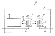
図1は、本発明の一実施形態による、圧電基板12上に製作した反射SAWフィルタ10の平面図である。反射SAWフィルタ10は、双方向入力トランスデューサ14と、出力双方向トランスデューサ16と、本発明による反射グレーティング18とを含む。入力トランスデューサ14および出力トランスデューサ16は、バス・バー22の対向する端部に結合された複数の均一間隔櫛形(すだれ状)電極フィンガ20を含む。反射SAWフィルタ10は、入力線24上の入力トランスデューサ14に印加され濾波(フィルタリング)される電気入力信号によって励起される。入力トランスデューサ14は、この電気信号を表面弾性波28に変換する。表面弾性波28は、出力トランスデューサ14から圧電基板12の表面に沿って外に向かって伝搬する。
FIG. 1 is a plan view of a
弾性波エネルギ28の約半分が出力トランスデューサ16によって受け取られ、再度電気エネルギに変換されて、出力線30上に送られる。弾性波エネルギ28の残りの半分は、反射グレーティング18によって受け取られ、反射され入力トランスデューサ14を通して出力トランスデューサ16に達し、ここで再度電気エネルギに変換される。実用的な実施形態では、フィルタ10は、2つの入力トランスデューサおよび2つの出力トランスデューサを含み、出力トランスデューサ16における信号相殺を補正するようにしている。これは、当業者には周知のことである。以下に説明するが、反射グレーティング18は、特定の周波数帯域に対して反射グレーティング18の反射能力を最適化するディザ格子線を用いている。
Approximately half of the
尚、フィルタ10が適正に動作するために、第2反射トラックを含ませるとよいことを注記しておく。この第2反射トラックも、入力トランスデューサ、出力トランスデューサ、および反射グレーティングを含む。こうする場合、2つの入力トランスデューサは同じ極性を有し、2つの出力トランスデューサは逆の極性を有する。したがって、対応する入力トランスデューサから出力トランスデューサによって直接受け取られ、反射グレーティングによって反射されない表面弾性波は、フィルタの出力トランスデューサにおいて互いに同相となり、このため相殺される。何故なら、2つの出力トランスデューサは逆の極性を有するからである。反射グレーティングによって反射された弾性波は、互いに180゜位相がずれて、対応する出力トランスデューサに到達し、2つの出力トランスデューサは逆の極性を有するので、出力において加算し合う。グレーティング反射間の180゜の位相差は、様々な技法で与えることができ、一方のトラックにおいて他方のトラックに対して遅延を与え、2系統のトラックにおいて、反射弾性波が伝搬する距離にλ/2の差を付けるようにすることが含まれる。この遅延は、2系統のトラックにおける反射グレーティング間にλ/4のオフセットを設けることによって得ることができる。
It should be noted that a second reflective track may be included for the
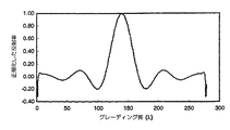
図2は、サンプリング周期がλ/4の反射グレーティング18の反射率関数を示すグラフである。本発明によれば、サンプリング周期は、各N波長毎にM本の格子線(Nλ/M)によって定義され、λは、フィルタの帯域幅の中心周波数における波長であり、MおよびNは整数であって、M>Nである。サンプリング周期の例には、λ/4、λ/3、2λ/5、3λ/7、3λ/8、4λ/7、および5λ/8が含まれるが、これらに限定される訳ではない。各サンプリング周期の特徴は、反射グレーティング18の格子線が均一に離間されている、または、周期的である場合、つまり、ディザ処理されていない場合、グレーティング18はネット(有効)反射率を有さないということである。トランスデューサの臨界寸法CDは、格子線周期NλMに比例する。λ=V/f0であるので、f0はN/(M*CD)に比例する。比率N/Mが大きい程、所与のCDに対する格子の中心周波数は高くなる。
FIG. 2 is a graph showing the reflectance function of the reflection grating 18 having a sampling period of λ / 4. According to the present invention, the sampling period is defined by M grid lines (Nλ / M) for each N wavelength, where λ is the wavelength at the center frequency of the filter bandwidth, and M and N are integers. And M> N. Examples of sampling periods include, but are not limited to, λ / 4, λ / 3, 2λ / 5, 3λ / 7, 3λ / 8, 4λ / 7, and 5λ / 8. A characteristic of each sampling period is that if the grating lines of the
先に説明したように、反射グレーティングの格子線がNλ/M配列(orientation)を有する場合、格子線内部における表面弾性波の反射は適正な位相を有して減算的に干渉するため、有効反射率は得られない。所望の反射率を得るには、ディザ処理を行う。即ち、以下で説明する所定のディザ関数に応じて、格子線の位置を均一な間隔に対して変化させる。ディザ関数の選択は、反射される弾性波の振幅および位相を制御して、これらが互いに結合され、対象の周波数帯域の中心において所望の反射が発生するように行う。周波数応答の形状は、理想的な特性のフィルタが得られる、理想的な反射率関数となる。 As described above, when the grating line of the reflection grating has an Nλ / M orientation, the reflection of the surface acoustic wave inside the grating line has an appropriate phase and interferes in a subtractive manner. The rate is not obtained. In order to obtain a desired reflectance, dithering is performed. That is, the positions of the grid lines are changed with respect to the uniform interval according to a predetermined dither function described below. The dither function is selected by controlling the amplitude and phase of the reflected elastic waves so that they are coupled together to produce the desired reflection at the center of the frequency band of interest. The shape of the frequency response is an ideal reflectance function that provides a filter with ideal characteristics.
図3は、図2に示す反射特性を有する反射グレーティング18の周波数応答を示すグラフである。図3に示すグラフは、当技術分野では、「ブリックウォール(brick wall)」周波数応答として知られているものを示す。ブリックウォール周波数応答は、急峻な遷移縁および狭い帯域幅を有する理想的な応答である。図2の反射関数を有する反射グレーティングは、図3に示すような「ブリックウォール」周波数応答を生成する。
FIG. 3 is a graph showing the frequency response of the
図4は、フィルタ10において、反射グレーティング18の代わりに用いることができる、本発明による反射グレーティング36の平面図である。図5は、グレーティング36について、ディザ処理した反射器の強度のグレーティング位置に対する関係を示すグラフである。グラフの線48は、グレーティング36内のそれぞれの位置における反射表面波の振幅および位相を特定する。以下で説明するが、反射グレーティング36は、入射表面弾性波32が逆方向に反射されて、対象の周波数帯域に対して所望の振幅および位相を有する反射表面弾性波34となるような、反射率関数を備えている。
FIG. 4 is a plan view of a
反射グレーティング36は、一連の離間した格子線38を含み、それらの間にはギャップ40が規定されている。格子線38およびギャップ40の幅は、先に説明したように、各Nλ毎にM本の格子線38を配した場合の均一な格子間隔に基づく。均一な即ち周期的な格子線配列を得るには、格子線38およびギャップ40は全て、表面弾性波32の伝搬方向に同じ幅を有する。このため、格子線の間隔が均一であると、有効反射率は得られない。本発明の教示によれば、格子線38の一部を均一な間隔に対してディザ処理して、特定の中心周波数に対して所望の有効反射率(位相および振幅)を得るようにする。格子36内のディザ格子線44は、陰影によって、ディザ処理していない、即ち、均一格子線46とは区別されている。
The
この実施形態では、格子線38の間隔はサンプリング周期42によって特定され、各サンプリング周期42は、中心周波数の1波長(λ)に等しい距離にわたって、間隔をおいて配置された4本の格子線38を含む。更に、この実施形態では、各格子線38および間隔が均一なギャップ40は、フィルタリングする中心周波数に対して、λ/8の幅を有する。図4および図5における垂直グラフ線は、サンプリング周期42の分離を識別する。一実施形態では、グレーティング36は275のサンプリング周期を有する。即ち、その長さは275λである。
In this embodiment, the spacing of the grid lines 38 is specified by a sampling period 42, each sampling period 42 being spaced four
格子線38のディザ処理は所定のシーケンスに従う。例えば、垂直グラフ線50および52の間では、各サンプリング周期42における格子線38のディザ処理は、1つのディザ配列を有し、垂直グラフ線52および54間では、各サンプリング周期42における格子線38のディザ処理は別の配列を有し、これらのシーケンスは、反射グレーティング36全体にわたって交互に現れる。反射率関数の位相は、線52の一方側から他方側までに180゜変化する。
Dithering of the grid lines 38 follows a predetermined sequence. For example, between the
本発明によれば、サンプリング周期42における格子線38のディザ処理は、−1および1の間の数値によって規定される。0は、格子線38には均一間隔に対してディザ処理が行われていないことを意味し、正の数値は、格子線38を右側に一定量だけディザ処理したことを意味し、負の数値は、格子線38を左側に一定量だけディザ処理したことを意味する。この例では、−1および1のディザ処理は、格子線38をディザ処理可能な最大距離を表す。この実施形態では、−1および1のディザ処理は、ギャップ40の半分である。最大ディザ処理量は、格子の最小ギャップである臨界寸法がリソグラフィの実現可能な限界内である限り、ギャップの半分よりも多くすることも可能である。
According to the present invention, the dithering of the
垂直グラフ線50および52間のサンプリング周期42におけるディザ処理の配列は、シーケンス(0、0、1、−1)によって特定される。ディザ・シーケンスにおける値は、サンプリング周期内における各格子線の相対的な変位を示す。この意味は、最初と2番目の格子線38にはディザ処理が行われておらず、3番目の格子線は0と最大量との間で右側にディザ処理することができ、4番目の格子線38は、0と最大量との間で左側にディザ処理できるということである。しかしながら、同じ周期内では、3番目および4番目の格子線双方に行われるディザ処理は、同じ量である。垂直グラフ線52および54間のサンプリング周期42におけるディザ処理の配列は、ディザ・シーケンス(−1、1、0、0)を有する。この意味は、最初の格子線38は0と最大距離との間で左側にディザ処理することができ、2番目の格子線は0と最大距離との間で右側にディザ処理することができ、3番目および4番目の格子線は均一な間隔に対してディザ処理されないということである。しかしながら、同じ周期内では、最初および2番目の格子線双方に行われるディザ処理は、同じ量である。グラフ線48は、このディザ・シーケンスに対する反射の大きさおよび位相を示す。SWA伝搬速度Vはディザ処理した規模の関数であるので、SAWが適正にグレーティングを伝搬するためには、ディザ・シーケンスに応じて各サンプリング周期のλを調節しなければならない。
The arrangement of dithering in the sampling period 42 between the
図6は、フィルタ10における反射グレーティング18として用いることができる、本発明の別の実施形態による反射グレーティング70の上面図である。図7は、グレーティング70について、ディザ反射強度のグレーティング位置に対する関係を示すグラフである。これについては、以下で説明する。反射グレーティング70は、先に説明した反射グレーティング36と同様であり、同じ要素を識別する際には、同様の参照番号を用いることとする。反射グレーティング70のサンプリング周期42では、図5および図7におけるグラフ線48で示したように、反射グレーティング36と同じ反射率関数が得られる。
FIG. 6 is a top view of a
また、反射グレーティング70も、1つのサンプリング周期42に4本の格子線38を含み、Nλ/M=λ/4となる。グラフ線50および52間の格子線38のディザ・シーケンスは、(1、−1、1、−1)であり、グラフ線52および54間の格子線38のディザ・シーケンスは、(−1、1、−1、1)である。したがって、グレーティング70における格子線38の全てを、0と最大量との間で、右側または左側のいずれかにディザ処理することができる。しかしながら、同じ周期内では、4本の格子線に行われるディザ処理は全て同じ量である。こうして、異なるディザ・シーケンスによって、同じ反射率関数を設けることができる。
The
各反射のディザ処理方向を逆にすることによって、反射位相は180゜変化する。一般に、1つのサンプリング周期42の反射中心を、別の周期のそれに対して空間的にλ/4だけオフセットすると、2つの周期の反射率は、180゜位相ずれとなる。図4〜図7から、各サンプリング周期42内におけるディザ・シーケンスが減少するに従って、周期42の反射率の大きさも減少することは明白である。 By reversing the dithering direction of each reflection, the reflection phase changes by 180 °. In general, if the reflection center of one sampling period 42 is spatially offset by λ / 4 with respect to that of another period, the reflectance of the two periods is 180 ° out of phase. 4-7, it is clear that as the dither sequence within each sampling period 42 decreases, the magnitude of the reflectivity of period 42 also decreases.
図8は、フィルタ10における反射グレーティング18として用いることができる、本発明の別の実施形態による反射グレーティング80の上面図である。同じように、図9は、グレーティング80について、ディザ反射強度のグレーティング位置に対する関係を示すグラフである。前述のように、同様の参照番号は、同様の要素を表す。反射グレーティング80は、図4および図6に示したサンプリング周期42とは異なるサンプリング周期82を有し、図5、図7および図9に示すように、同じ反射率関数を設けるために用いることができる。この実施形態では、各サンプリング周期82は、5本の格子線38を含み、3λの幅を有する。更に、各格子線38および各ギャップ40の幅は、3λ/10である。グラフ線50および52の間にある反射グレーティング80の区間に対するディザ・シーケンスは、(−1、−0.35、−0.35、0.8、1)であり、格子線52および54の間にある反射グレーティング80のディザ・シーケンスは、(0.35、1、0、−0.8、0.35)である。この場合も、ディザ・シーケンスにおける値は、1サンプリング周期内における各格子線の相対的な変位を示す。
FIG. 8 is a top view of a
格子線38は、適した技法であればそのいずれによっても、圧電基板上に形成することができる。例えば、図10(a)は、ディザ格子線92を有し、それらの間にギャップ94を規定した反射グレーティング90の平面図である。格子線92は、それらの終端において、図示のように、対向する端部バス・バー96、98に結合され、格子短絡回路となっている。反射グレーティング36、70、80は、端部バス・バーを有しておらず、したがって開放回路設計となっている。この実施形態では、格子線92およびバス・バー96、98は、基板上にデポジション(堆積)された金属である。
The grid lines 38 can be formed on the piezoelectric substrate by any suitable technique. For example, FIG. 10A is a plan view of a
図10(b)は、本発明による反射グレーティング100の平面図であり、一連の離間されたディザ格子線102を含み、これらの間にギャップ104を規定している。格子線102は、金属のようないずれかの適した格子材料、基板上にデポジションされるいずれかの適した物質、基板(下方)にエッチングした溝、基板内へのイオン打ち込み(インプランテーション)、または所望のディザ・パターンが得られる、基板上のあらゆる種類の擾乱(disturbance)即ち変動によって形成することができる。
FIG. 10 (b) is a plan view of a
図10(c)は、テーパー状の格子線112を含むグレーティング110の平面図である。テーパー状の格子線112は、多数の通信チャネルの隣接する周波数帯域に適した反射率チャネルを設ける。格子線112は、N個の格子チャネルを上から下まで、チャネルの波長が小さい順または大きい順に接続することによって、構成することができる。図10(a)および図10(b)に示した反射グレーティングの多様な実施形態は、テーパー状反射グレーティング112にも適用することができる。
FIG. 10C is a plan view of the grating 110 including the tapered
これまでの説明は、本発明の実施形態例を開示し、説明したに過ぎない。このような説明ならびに添付図面および特許請求の範囲から、変更や改変も、特許請求の範囲に規定する本発明の精神および範囲から逸脱することなく、本発明において可能であることを、当業者であれば容易に理解するであろう。 The foregoing description merely discloses and describes exemplary embodiments of the present invention. From such description and the accompanying drawings and claims, those skilled in the art will recognize that changes and modifications can be made in the present invention without departing from the spirit and scope of the invention as defined in the claims. It will be easy to understand.
Claims (9)
圧電基板と、
前記基板上に配置された反射グレーティング構造であって、間にギャップを規定する一連の格子線を含む、反射グレーティング構造と、
を備え、前記格子線を、ある格子線幅およびギャップ幅によって規定される均一または周期的間隔の配列に対して方向付けし、所定数の前記格子線を、均一間隔に対してディザ処理して、対象の周波数帯域に対して前記反射波の振幅および位相を設定する反射率関数を提供し、ある数の前記格子線が、所定の反復サンプリング周期を規定し、該サンプリング周期が同一のサンプリング波長λを有し、N波長毎にM本の格子線によって規定され(Nλ/M)、λは対象の周波数帯域の中心周波数の波長であり、MおよびNは整数であって、M>Nである、反射器。 A reflector for reflecting acoustic waves,
A piezoelectric substrate;
A reflective grating structure disposed on the substrate, comprising a series of grid lines defining a gap therebetween; and
Directing the grid lines to an array of uniform or periodic intervals defined by a grid line width and gap width, and dithering a predetermined number of the grid lines to uniform intervals provides a reflectivity function that sets the amplitude and phase of the reflected wave with respect to frequency band of interest, the grid lines of a certain number, defines a predetermined repetition sampling period, the sampling period is the same sampling Has a wavelength λ and is defined by M grid lines every N wavelengths (Nλ / M), where λ is the wavelength of the center frequency of the frequency band of interest, M and N are integers, and M> N The reflector.
Applications Claiming Priority (1)
| Application Number | Priority Date | Filing Date | Title |
|---|---|---|---|
| US10/377,333 US6842091B2 (en) | 2003-02-28 | 2003-02-28 | Weighted SAW reflector grating using dithered acoustic reflectors |
Publications (2)
| Publication Number | Publication Date |
|---|---|
| JP2004266828A JP2004266828A (en) | 2004-09-24 |
| JP4666928B2 true JP4666928B2 (en) | 2011-04-06 |
Family
ID=32771524
Family Applications (1)
| Application Number | Title | Priority Date | Filing Date |
|---|---|---|---|
| JP2004044640A Expired - Lifetime JP4666928B2 (en) | 2003-02-28 | 2004-02-20 | Weighted SAW reflection grating using dithered acoustic reflector |
Country Status (3)
| Country | Link |
|---|---|
| US (1) | US6842091B2 (en) |
| EP (1) | EP1458093A1 (en) |
| JP (1) | JP4666928B2 (en) |
Families Citing this family (8)
| Publication number | Priority date | Publication date | Assignee | Title |
|---|---|---|---|---|
| US8143681B2 (en) * | 2006-04-20 | 2012-03-27 | The George Washington University | Saw devices, processes for making them, and methods of use |
| US20100007444A1 (en) * | 2006-04-20 | 2010-01-14 | Anis Nurashikin Nordin | GHz Surface Acoustic Resonators in RF-CMOS |
| US20090124513A1 (en) * | 2007-04-20 | 2009-05-14 | Patricia Berg | Multiplex Biosensor |
| US8018010B2 (en) * | 2007-04-20 | 2011-09-13 | The George Washington University | Circular surface acoustic wave (SAW) devices, processes for making them, and methods of use |
| US8960004B2 (en) | 2010-09-29 | 2015-02-24 | The George Washington University | Synchronous one-pole surface acoustic wave resonator |
| JP6092535B2 (en) * | 2012-07-04 | 2017-03-08 | 太陽誘電株式会社 | Lamb wave device and manufacturing method thereof |
| US9152897B1 (en) * | 2014-04-16 | 2015-10-06 | Eastman Kodak Company | Printing an image on a substrate |
| US11545960B2 (en) | 2018-11-16 | 2023-01-03 | Skyworks Solutions, Inc. | Multi-mode surface acoustic wave filter with slanted acoustic reflectors |
Citations (5)
| Publication number | Priority date | Publication date | Assignee | Title |
|---|---|---|---|---|
| JPS5547718A (en) * | 1978-09-22 | 1980-04-04 | Philips Nv | Elastic wave resonator |
| US5289073A (en) * | 1992-11-09 | 1994-02-22 | The United States Of America As Represented By The Secretary Of The Army | Unidirectional surface acoustic wave transducer |
| US5831494A (en) * | 1996-12-12 | 1998-11-03 | Sawtek Inc. | Dual track low-loss reflective saw filter |
| JPH1188112A (en) * | 1997-09-12 | 1999-03-30 | Fujitsu Ltd | Surface acoustic wave element |
| JP2000165184A (en) * | 1998-11-20 | 2000-06-16 | Fujitsu Ltd | Surface acoustic wave element |
Family Cites Families (8)
| Publication number | Priority date | Publication date | Assignee | Title |
|---|---|---|---|---|
| DE3209962A1 (en) * | 1982-03-18 | 1983-09-29 | Siemens AG, 1000 Berlin und 8000 München | ELECTRONIC COMPONENT WORKING WITH ACOUSTIC SHAFTS |
| ATE113425T1 (en) * | 1989-11-14 | 1994-11-15 | Siemens Ag | SURFACE WAVE REFLECTOR FILTER. |
| FR2682833B1 (en) * | 1991-10-18 | 1993-12-03 | Thomson Csf | SURFACE WAVE FILTER WITH FOLDED ACOUSTIC PATH. |
| DE4213117A1 (en) * | 1992-04-21 | 1993-10-28 | Siemens Ag | Weighted reflector structure for SAW devices - allows reflectivity to be varied from max. to zero by positioning of strips more closely in pairs having different distances between them |
| DE4306825A1 (en) | 1993-03-04 | 1994-09-08 | Siemens Ag | Surface wave resonator filter |
| DE4419722C1 (en) * | 1994-06-06 | 1996-02-22 | Siemens Ag | Filter working with surface acoustic waves |
| DE19548042C2 (en) * | 1995-12-21 | 1999-11-04 | Siemens Matsushita Components | Filter working with surface acoustic waves -OFW filter- |
| US6104260A (en) * | 1997-12-22 | 2000-08-15 | Matsushita Electric Industrial Co., Ltd. | Surface acoustic wave filter with first and second filter tracks and balanced or unbalanced terminals |
-
2003
- 2003-02-28 US US10/377,333 patent/US6842091B2/en not_active Expired - Fee Related
- 2003-11-18 EP EP03026558A patent/EP1458093A1/en not_active Withdrawn
-
2004
- 2004-02-20 JP JP2004044640A patent/JP4666928B2/en not_active Expired - Lifetime
Patent Citations (5)
| Publication number | Priority date | Publication date | Assignee | Title |
|---|---|---|---|---|
| JPS5547718A (en) * | 1978-09-22 | 1980-04-04 | Philips Nv | Elastic wave resonator |
| US5289073A (en) * | 1992-11-09 | 1994-02-22 | The United States Of America As Represented By The Secretary Of The Army | Unidirectional surface acoustic wave transducer |
| US5831494A (en) * | 1996-12-12 | 1998-11-03 | Sawtek Inc. | Dual track low-loss reflective saw filter |
| JPH1188112A (en) * | 1997-09-12 | 1999-03-30 | Fujitsu Ltd | Surface acoustic wave element |
| JP2000165184A (en) * | 1998-11-20 | 2000-06-16 | Fujitsu Ltd | Surface acoustic wave element |
Also Published As
| Publication number | Publication date |
|---|---|
| EP1458093A1 (en) | 2004-09-15 |
| US20040169569A1 (en) | 2004-09-02 |
| US6842091B2 (en) | 2005-01-11 |
| JP2004266828A (en) | 2004-09-24 |
Similar Documents
| Publication | Publication Date | Title |
|---|---|---|
| KR100817849B1 (en) | Elastic surface wave resonator and elastic surface wave filter using the same | |
| JP4284175B2 (en) | Surface wave transducer with improved suppression of fault excitation | |
| EP1467484A2 (en) | Surface acoustic wave transducer | |
| WO2004054102A1 (en) | Surface wave devices with low passband ripple | |
| JP4666928B2 (en) | Weighted SAW reflection grating using dithered acoustic reflector | |
| CN114268294B (en) | SAW device including hybrid weighting type reflection grating and hybrid weighting type reflection grating | |
| JP3414373B2 (en) | Surface acoustic wave device | |
| KR20020079927A (en) | Surface wave converter with optimised reflection | |
| EP1207621B1 (en) | Transversal surface acoustic wave filter | |
| JP4696312B2 (en) | Dual track SAW reflector filter using weighted reflective grating | |
| CA2375596A1 (en) | Longitudinally coupled surface acoustic wave filter | |
| US6534896B2 (en) | Spatial harmonic transducers for surface wave devices | |
| JP4713087B2 (en) | Weighted SAW reflector using distributed acoustic reflection dots | |
| JP4379143B2 (en) | Transversal surface acoustic wave filter | |
| JP2005278154A (en) | One-directional surface acoustic wave transducer and surface acoustic wave device using it | |
| JP3451234B2 (en) | Transversal surface acoustic wave filter | |
| JP4506394B2 (en) | Unidirectional surface acoustic wave transducer and surface acoustic wave device using the same | |
| US6559739B2 (en) | String weighted surface acoustic wave transducer | |
| Jian et al. | A new type SPUDT SAW for use in high frequency around 2 GHz | |
| WO1998027647A1 (en) | Surface wave device filters using resonant single phase unidirectional transducers | |
| JP2005268962A (en) | Unidirectional surface acoustic wave transducer and surface acoustic wave device employing the same | |
| RU2171010C2 (en) | Filter on surface acoustic waves with quasi-fan converters | |
| JPH06260880A (en) | Surface acoustic wave filter | |
| JP3901879B2 (en) | Surface acoustic wave filter | |
| JP2001094394A (en) | Surface acoustic wave reflector |
Legal Events
| Date | Code | Title | Description |
|---|---|---|---|
| A621 | Written request for application examination |
Free format text: JAPANESE INTERMEDIATE CODE: A621 Effective date: 20070116 |
|
| A131 | Notification of reasons for refusal |
Free format text: JAPANESE INTERMEDIATE CODE: A131 Effective date: 20091113 |
|
| A521 | Request for written amendment filed |
Free format text: JAPANESE INTERMEDIATE CODE: A523 Effective date: 20100215 |
|
| A02 | Decision of refusal |
Free format text: JAPANESE INTERMEDIATE CODE: A02 Effective date: 20100520 |
|
| A521 | Request for written amendment filed |
Free format text: JAPANESE INTERMEDIATE CODE: A523 Effective date: 20100921 |
|
| A911 | Transfer to examiner for re-examination before appeal (zenchi) |
Free format text: JAPANESE INTERMEDIATE CODE: A911 Effective date: 20101104 |
|
| TRDD | Decision of grant or rejection written | ||
| A01 | Written decision to grant a patent or to grant a registration (utility model) |
Free format text: JAPANESE INTERMEDIATE CODE: A01 Effective date: 20101213 |
|
| A01 | Written decision to grant a patent or to grant a registration (utility model) |
Free format text: JAPANESE INTERMEDIATE CODE: A01 |
|
| A61 | First payment of annual fees (during grant procedure) |
Free format text: JAPANESE INTERMEDIATE CODE: A61 Effective date: 20110111 |
|
| FPAY | Renewal fee payment (event date is renewal date of database) |
Free format text: PAYMENT UNTIL: 20140121 Year of fee payment: 3 |
|
| R150 | Certificate of patent or registration of utility model |
Free format text: JAPANESE INTERMEDIATE CODE: R150 Ref document number: 4666928 Country of ref document: JP Free format text: JAPANESE INTERMEDIATE CODE: R150 |
|
| FPAY | Renewal fee payment (event date is renewal date of database) |
Free format text: PAYMENT UNTIL: 20140121 Year of fee payment: 3 |
|
| S111 | Request for change of ownership or part of ownership |
Free format text: JAPANESE INTERMEDIATE CODE: R313113 |
|
| FPAY | Renewal fee payment (event date is renewal date of database) |
Free format text: PAYMENT UNTIL: 20140121 Year of fee payment: 3 |
|
| R350 | Written notification of registration of transfer |
Free format text: JAPANESE INTERMEDIATE CODE: R350 |
|
| R250 | Receipt of annual fees |
Free format text: JAPANESE INTERMEDIATE CODE: R250 |
|
| R250 | Receipt of annual fees |
Free format text: JAPANESE INTERMEDIATE CODE: R250 |
|
| R250 | Receipt of annual fees |
Free format text: JAPANESE INTERMEDIATE CODE: R250 |
|
| R250 | Receipt of annual fees |
Free format text: JAPANESE INTERMEDIATE CODE: R250 |
|
| R250 | Receipt of annual fees |
Free format text: JAPANESE INTERMEDIATE CODE: R250 |
|
| R250 | Receipt of annual fees |
Free format text: JAPANESE INTERMEDIATE CODE: R250 |
|
| R250 | Receipt of annual fees |
Free format text: JAPANESE INTERMEDIATE CODE: R250 |
|
| R250 | Receipt of annual fees |
Free format text: JAPANESE INTERMEDIATE CODE: R250 |
|
| R250 | Receipt of annual fees |
Free format text: JAPANESE INTERMEDIATE CODE: R250 |
|
| R250 | Receipt of annual fees |
Free format text: JAPANESE INTERMEDIATE CODE: R250 |
|
| R250 | Receipt of annual fees |
Free format text: JAPANESE INTERMEDIATE CODE: R250 |