JP4666787B2 - Vibration detection apparatus and image shake correction apparatus - Google Patents
Vibration detection apparatus and image shake correction apparatus Download PDFInfo
- Publication number
- JP4666787B2 JP4666787B2 JP2001033668A JP2001033668A JP4666787B2 JP 4666787 B2 JP4666787 B2 JP 4666787B2 JP 2001033668 A JP2001033668 A JP 2001033668A JP 2001033668 A JP2001033668 A JP 2001033668A JP 4666787 B2 JP4666787 B2 JP 4666787B2
- Authority
- JP
- Japan
- Prior art keywords
- determination
- output
- image blur
- vibration
- offset
- Prior art date
- Legal status (The legal status is an assumption and is not a legal conclusion. Google has not performed a legal analysis and makes no representation as to the accuracy of the status listed.)
- Expired - Fee Related
Links
Images


Description
【0001】
【発明の属する技術分野】
本発明は、振動を検出する振動検出手段を有する振動検出装置及び像振れ補正装置の改良に関するものである。
【0002】
【従来の技術】
従来より、カメラを初めとする光学系の振れ補正、つまり手振れなどによる振動を抑制して像安定を行うための装置が提案されている。カメラ等に用いられる振れ補正方式のうちの一つの典型的なものとしては、振れセンサにて検出したカメラの振れ情報に基づき撮影光学系の一部、或いは全部を駆動して結像面上の像振れを抑制するというものである。
【0003】
ここで、前記振れセンサとしては、一般的に角速度センサ又は加速度センサ等が用いられている。このような角速度センサ又は加速度センサ自体は与えられた振動に対して微小な電圧しか出力されないために、該センサの外部に適当な増幅器を設けて、必要な電圧を出力するような構成をとっている。しかし、こうした振動を検出するセンサ、特にカメラなどにおいて一般的に使用されている圧電型振動ジャイロなどは、振動を与えないときの静止時の出力電圧(センサの基準電圧と静止時の出力電圧との差=ヌル電圧)が振動ジャイロの個々のばらつきや使用環境の変化により、特に使用温度により極めて大きく変化してしまう。よって、特に電源投入時に問題になることとして、出力信号を必要な電圧に増幅する際に、ヌル電圧を増幅してしまうことになり、特に高ゲインの増幅器を使用した場合には信号が飽和してしまう可能性がある。
【0004】
上記問題を解決する為に従来より開示されている方法としては、検出しようとする振動の周波数に対して許容できる低い周波数以下を角速度センサの出力からカットするハイパスフィルタ回路を設けて、このハイパスフィルタ回路を通過した信号を増幅器にて増幅する方法が一般的に取られている。
【0005】
また、上記従来例の改良として、ハイパスフィルタ回路を構成する大容量コンデンサを排除し、コスト上や実装上で有利な振動検出装置が特開平10−228043号公報に開示されている。これは、振動ジャイロからの出力をローパスフィルタ回路及び加算器及び増幅回路から成る回路を通じマイコンに入力し、マイコンは前記回路の出力信号が所定レベル範囲を超えているか及び基準レベルに対して偏っているかを判定するものである。所定レベル範囲を超えている又は基準レベルに対して偏っているときは、マイコンより制御信号を発生し、その信号によりD/A変換器の出力を制御する。このD/A変換器の出力は前記加算器に接続されており、出力信号を所定レベル範囲内及び基準レベルに調整する。このような構成により、電源投入時の不安定な出力を飽和させることなく増幅し、所望の出力値を得るようにしているものである。
【0006】
前述したようなD/A変換器を用いてセンサのオフセット成分を補償する構成の一例として、像振れ補正装置が一眼レフカメラの交換レンズ内に適用された従来例について、図7に示す。
【0007】
図7は、レンズ電気系として、レンズマイコン及び振れ補正系の具体的回路構成を示すブロック図である。
【0008】
振れを検出する角速度センサである振動ジャイロ1からの出力は、抵抗R1、抵抗R2、抵抗R3、コンデンサC1、コンデンサC2、オペアンプ2により構成される増幅部3を経てレンズマイコン4のA/D変換器5に入力される。前記増幅部3において、その増幅率は(R3/R1)により決定され、またノイズ除去のために2次高域遮断フィルタが形成されている。D/A変換部7は2個の8bit D/A変換器7a(D/A▲1▼),7b(D/A▲2▼)と抵抗R4,R5で構成されている。D/A変換器7aの出力端には抵抗R4が、D/A変換器7bの出力端には抵抗R5が、それぞれ接続されており、両抵抗の他端は共にオペアンプ2の非反転入力端子に接続されている。ここで、抵抗R4と抵抗R5の抵抗比は、例えば「R4:R5=1:110」程度に設定している。これはオフセット補償制御の分解能を考慮して決定する。
【0009】
電源投入初期時等には、振動ジャイロ1のオフセット成分補償演算のためにオフセット除去手段6(出力飽和回避制御部6a、制御データ記憶部6b、データ選択・制御部6cにより構成されている)が動作し、該オフセット除去手段6はD/A変換器7a及びD/A変換器7bの出力を制御する。D/A変換器7a及び7bの抵抗分割出力は増幅部3のオペアンプ2の非反転入力端子に接続されており、A/D変換器5の出力に応じて、D/A変換部7の出力が制御されることにより補正電圧が制御され振動ジャイロのオフセット成分が補償される。その後、ハイパスフィルタ(HPF)8、積分器9を経て角変位信号へと変換される。そして、補正レンズの位置を検知する位置センサ10の出力(増幅器11及びA/D変換器12を介する)が逆極性で加算されてフィードバック演算され、その信号がレンズマイコン4の出力ポートよりPWM信号としてPWM信号変換部13を介して出力され、コイルドライバ14によって補正レンズが駆動され、像振れを打ち消すようになっている。
【0010】
【発明が解決しようとする課題】
図8は、振動ジャイロに大きな振れが加わっておらず、安定した出力の場合((a)静止時)とパンニング等の大きな振れが生じた場合((b)パンニング時)の出力波形例である。
【0011】
図8(a)の静止時には、振動ジャイロの出力は所定の基準電圧に対して通常+α(又は−α:αはヌル電圧成分)だけ上乗せされた出力が出力される。前述したオフセット補償演算はこのαを基準になされている。しかし、図8(b)のパンニング時には、前記αに加えてパンニング成分である+β(又は−β)が上乗せされる。よって、このような状態でオフセット補償が行われる場合にはα+β(又はα−β,β−α,−α−β)を基準値として演算がなされることになる。
【0012】
つまり、像振れ補正装置にてパンニングや大振れ状態で上記オフセット補償演算がなされると、パンニングの出力成分と真のセンサオフセット成分の加算量をその時点のセンサオフセット量とみなしてオフセット補償演算を行ってしまうため、オフセット補償演算終了後にパンニング動作又は大振れ動作をやめると出力が目標値から大きくずれる可能性があり、場合によっては出力が飽和してしまうという問題点があった。
【0014】
本発明は、装置がパンニング状態や大振れ状態で振れ信号に重畳するオフセット成分の除去演算が行われても、 その後の像振れ補正動作に悪影響を及ぼすことのない像振れ補正装置を提供することを目的とする。
【0015】
【課題を解決するための手段】
本発明の像振れ補正装置は、振動を検出する振動検出手段と、該振動検出手段の出力のオフセット成分が除去された補正電圧を出力する手段と、前記補正電圧に基づいて前記振動検出手段の出力のオフセット成分の除去を行うオフセット除去手段と、を有する像振れ補正装置において、前記オフセット除去手段を動作させた後に、前記補正電圧を出力する手段からの出力が第一の判定時間の内に第一の判定範囲に収まっているかの判定を行い、該判定条件の内にあれば、防振動作開始を指示し、該判定条件の内になければ、前記オフセット除去手段を再び動作させるとともに、前記第一の判定時間の内に前記第一の判定範囲に収まっているかの判定を再び行う第一の判定及び制御手段と、防振動作の開始を指示した後に動作し、前記比較手段の出力が第二の判定時間の内に第二の判定範囲に収まっているかの判定を行い、該判定条件の内にあれば、防振動作を行い、該判定条件の内になければ、防振動作を一旦中断し、前記オフセット除去手段を再び動作させる第二の判定及び制御手段と、を有し、前記第二の判定時間は前記第一の判定時間より長く、前記第二の判定範囲は前記第一の判定範囲よりも広いことを特徴とする。
【0017】
【発明の実施の形態】
以下、本発明を図示の実施の形態に基づいて詳細に説明する。
【0018】
図1は本発明の実施の一形態に係るブロック図であり、像振れ補正装置が一眼レフカメラの交換レンズ内に搭載された場合を例にしている。
【0019】
同図において、101はレンズマイコンであり、カメラボディ側から通信用の接点109c(クロック信号用)、109d(ボディ→レンズ信号伝達用)を通じて通信を受け、その指令値によって、図1に示したような構成より成る振れ補正系102、フォーカス駆動系104、絞り駆動系105の動作を行わせる。前記振れ補正系102は、振れを検出する振れセンサ106、補正レンズ変位検出用の位置センサ107、及び、前記振れセンサ106と位置センサ107の出力を基にレンズマイコン101にて算出された制御信号によって補正レンズを駆動して振れ補正動作を行う振れ補正駆動系108から成る。また、124(SWIS)は振れ補正動作を選択する為の防振スイッチであり、振れ補正動作を選択する場合はこの防振スイッチ124をONにする。
【0020】
前記フォーカス駆動系104は、レンズマイコン101からの指令値によって、焦点調節用のレンズを駆動してフォーカシングを行う。前記絞り駆動系105は、レンズマイコン101からの指令値によって、絞りを設定された位置まで絞る又は開放状態に復帰させるという動作を行う。また、前記レンズマイコン101は、レンズ内の状態(フォーカス位置、絞り値の状態など)や、レンズに関する情報(開放絞り値、焦点距離、測距演算に必要なデータなど)を通信用の接点109e(レンズ→ボディ信号伝達用)よりボディ側に伝達することも行う。
【0021】
前述のレンズマイコン101、振れ補正系102、フォーカス駆動系104、絞り駆動系105により、レンズ電気系110が構成される。そして、このレンズ電気系110に対しては、電源接点109a、グランド接点109bを通じてカメラ内電源118から給電が行われる。
【0022】
カメラボディ内部には、カメラボディ内電気系111として、測距部112、測光部113、シャッタ部114、表示部115、その他の制御部116、及び、これらの動作開始、停止などの管理、露出演算、測距演算などを行うカメラマイコン117が内蔵されている。これらカメラボディ内電気系111に対しても、その電源はカメラ内電源118より供給される。また、121(SW1)は測光や測距を開始させる為のスイッチであり、122(SW2)はレリーズ動作を開始させる為のレリーズスイッチであり、これらは一般的には2段ストロークスイッチであって、レリーズボタンの第1ストロークでスイッチ121がONし、第2ストロークでレリーズスイッチ122がONになるように構成されている。123(SWM)は露出モード選択スイッチであり、露出モード変更は、該スイッチのON,OFFで行ったり、該スイッチ123と他の操作部材との同時操作により行う方法等がある。
【0023】
図2は、レンズ電気系110のレンズマイコン101及び振れ補正系102の具体的回路構成を示すブロック図である。
【0024】
構成としては図7のブッロク図の構成とほぼ同じであるので、図7の符号に500を加えた番号を付し、その詳細な説明は省略する。図7と異なる部分としては、第一の判定・制御部520と第二の判定・制御部521がA/D変換器505とハイパスフィルタ(HPF)508の間に介入されている点である。
【0025】
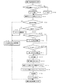
図3は、図2のレンズマイコン504内での具体的な処理動作を示したフローチャートである。
【0026】
ここで、像振れ補正動作は一定周期毎に発生する割り込み処理によって行われる。そして、第1の方向、例えばピッチ方向(縦方向)の制御と、第2の方向、例えばヨー方向(横方向)の制御を交互に行う。割り込みが発生すると、レンズマイコン504は図3に示すフローチャートのステップ#101からの動作を開始する。
【0027】
まず、ステップ#101において、今回の制御方向はピッチ方向であるかヨー方向であるかの判定を行う。ピッチ方向であればステップ#102へ進み、各種フラグや係数、計算結果等をピッチデータとして読み書きできるようにデータアドレスを設定してステップ#104へ進む。また、ヨー方向であればステップ#103へ進み、各種フラグや係数、計算結果等をヨーデータとして読み書きできるようにデータアドレスを設定してステップ#104へ進む。
【0028】
ステップ#104へ進むと、角速度センサである振動ジャイロ501の出力をA/D変換し、その結果をRAMに予め定義されたAD_DATA に格納する。そして、次のステップ#105において、像振れ補正開始の指示が為されたか否かを判定する。これは、例えばスイッチSWISのONとスイッチSW1のONのANDによって像振れ補正開始とする。像振れ補正開始の指示が為されていればステップ#106へ進み、指示が為されていなければステップ#118へ進む。ここでは像振れ補正開始の指示が為されており、ステップ#106へ進むものとする。また同時に、振動ジャイロ501及び増幅部503及びD/A変換器507a及びD/A変換器507bに給電動作が行われる(不図示)。
【0029】
ステップ#106へ進むと、オフセット補償演算終了フラグの判定を行う。オフセット補償演算が終了していればHレベル、終了していなければLレベルとなっている。フラグがLレベルであればステップ#107へ進み、振動ジャイロ501の出力をダイナミックレンジ内に収め(飽和を回避)かつ所定の目標値に出力させるため、オフセット補償演算を行う。詳細動作は、図4のフローチャートを基に別途説明する。この演算後はステップ#118へ進む。
【0030】
また、フラグがHレベルでればオフセット補償演算は終了しているので、ステップ#106からステップ#108へ進み、防振動作開始フラグの判定を行う。防振動作開始が指示されていればHレベル、指示されていなければLレベルとなっている。フラグがLレベルであればステップ#109へ進み、振動ジャイロ1について第一の判定・制御部520にて増幅出力の第一の判定及び制御を行う。なお、ステップ#108で参照した防振動作開始フラグは該ステップ#109における制御の中で決定されている。つまり、第一の判定結果に基づいて防振動作開始の指示を出している。第一の判定を行う理由、又詳細動作については、図5のフローチャートを基に別途説明する。その後はステップ#118へ進む。
【0031】
上記ステップ#108にてフラグがHレベルであることを判定すると、防振動作開始であるのでステップ#110へ進み、防振動作開始後の第二の判定の動作状況が反映されている第二の判定終了フラグの判定を行う。第二の判定が終了していればHレベル、終了していなければLレベルとなっている。フラグがLレベルであればステップ#111へ進み、さらに判定の精度を上げるために、防振動作開始後の振動ジャイロ1の増幅出力について第二の判定・制御部521にて第二の判定及び制御を行う。第二の判定を行う理由、又詳細動作については、図6のフローチャートを基に別途説明する。
【0032】
上記ステップ#110にてフラグがHレベルでれば第二の判定は終了しているので直ちにステップ#112へ進み、さらにDC成分のカットのため、ハイパスフィルタ(HPF)演算を行う。そして、次のステップ#113において、防振制御のための積分演算を行い、像振れの角変位信号(BURE_DATA )へ変換する。続くステップ#114においては、補正レンズの位置を検知する位置センサ510の出力を取り込み、A/D変換する(変換後=PSD_DATA)。
【0033】
次のステップ#115においては、フィードバック演算{(BURE_DATA )−(PSD_DATA)}を行う。そして、ステップ#116において、安定な制御系にするために位相補償演算を行い、次のステップ#117において、PWM変換部513よりコイルドライバ514へPWM出力を行う。これにより、防振制御が為され、像振れが補正されることになる。
【0034】
上記ステップ#105にて像振れ補正開始の指示が為されていなければ、前述したようにステップ#118へ進む。そして、このステップ#118においては、ハイパスフィルタ(HPF)演算、積分演算の初期化及び、タイマー1,2のクリア動作を行う。このステップにおいては像振れ補正動作はなされず、補正レンズは所定の位置に通電保持されている。
【0035】
以上のステップ#101〜#118により、像振れ補正制御がなされる。
【0036】
次に、前述した図3のステップ#107のオフセット補償演算について、図4のフローチャートを基に説明する。
【0037】
まず、ステップ#201において、D/A変換部507から初期出力を出力させるための設定がなされているか否かを判定する。これは例えばフラグのH又はLレベルで判定する。未設定で出力されていなければステップ#202へ進み、設定されていれば直ちにステップ#203へ進む。
【0038】
ステップ#202へ進むと、D/A変換部507から初期出力を出力させるために該D/A変換部507に初期値を設定する。ここで、初期値の設定方法としては、前述したように例えばそのセンサの基準電圧値とする。ここでは約1.35Vを出力するように設定を行う。D/A変換部507のD/A値の基準電圧を両者D/A変換器ともに、例えば3.0 Vとすると、8bit =256 LSB の分解能を持つことから、1.35V=115 LSB となり、その値をD/A変換器507aに設定し、他方のD/A変換器507bは0レベル出力とするため0LSB を設定する。
【0039】
次のステップ#203においては、振動ジャイロ1の信号のA/D値がダイナミックレンジ内に収まっているか否かの判定を行う。ここでA/D変換器505のA/D基準電圧が例えば 3.6Vであるとすると、A/D値が 3.5V以上であるか否かの判定を行う。 3.5V以上であれば出力は飽和に近い、又は飽和している可能性が高いのでステップ#204へ進み、 3.5V未満であればステップ#205へ進む。
【0040】
ステップ#204においては、A/D値はダイナミックレンジ内に収まらず、Hレベル側に飽和している可能性が高いので、オペアンプ502の非反転入力端子に接続されているD/A変換部507の出力を変更してA/D値が飽和しないように出力を制御する。増幅後出力の可変量としては、一回のD/A変換器の制御で、A/Dの基準電圧量を超えないような変更量に設定するのが好ましい。前述したように、A/D変換器505のA/D基準電圧が例えば 3.6Vであるとすると、 3.6V未満の変更量が好ましい。これは、まず初めに飽和している出力を飽和しない任意のレベルに出力させることが目的であるため、可能な限り少ない電圧変更回数にするためである。ここで、増幅部503の増幅率(R3/R1で決定される)を例えば64倍としたとき、オペアンプ502の非反転入力端子をΔVrefだけ変更すると増幅出力(A/D変換前出力)は、
(増幅部503の増幅率+1)×ΔVref=65×ΔVref
だけ変化する。増幅後の出力変化量を例えば 3.0Vとすれば、ΔVref=0.0462V となる。よって、D/A変換部507の出力を「ΔVref=0.0462V 」変化させれば増幅後の出力は 3.0V変化することになる。D/A変換部507のD/A変換器507a及び507bは「8bit =256 LSB 」の分解能を持つことから「0.0462V ≒4LSB」だけ設定値を変更する。ここでは、D/A変換器507aの現在の設定値から「0.0462V ≒4LSB」だけ減算し設定する。一方、他方のD/A変換器507bは何もせずそのままとする。これにより増幅出力は 3.0V分減少する。
この後、オフセット補償演算を一旦終了する。
【0041】
ステップ#205へ進むと、A/D値が 0.1V以上であるか否かの判定を行う。 0.1V以上であれば出力は飽和しておらずダイナミックレンジ内にあるのでステップ#207へ進む。一方、 0.1V以下であればLレベル側に飽和している可能性が高いのでステップ#206へ進む。
【0042】
ステップ#206へ進むと、A/D値はダイナミックレンジ内に収まらず、Hレベル側に飽和している可能性が高いので、オペアンプ502の非反転入力端子に接続されているD/A変換部507の出力を変更してA/D値が飽和しないように出力を制御する。ここでは、D/A変換器507aのみ、現在の設定値に0.0462V ≒4LSBだけ加算し設定する。一方、他方のD/A変換器507bは何もせずそのままとする。これにより増幅出力は 3.0V分増加する。この後、オフセット補償演算を一旦終了する。
【0043】
つまり、上記ステップ#204又は#206を複数回行うことにより、増幅出力の飽和を回避する(このステップ#204,#206の処理を行うのが出力飽和回避制御部506aである)。また、同ステップにおいてはD/A変換器507aのみを変化させ、増幅出力がダイナミックレンジ内に収まるよう粗調整していることになる。
【0044】
次のステップ#207へ進むと、A/D値が 0.1V以上 3.5V未満であるので、この時点でセンサ増幅出力は飽和しないダイナミックレンジ内に存在している。そして、この出力が目標値、例えば 1.8V± 0.1V以内に存在するか否かを判定する。ここでは目標値±0.1 V以内に収めるようにしているが、より狭い範囲に限定しても良い。前記範囲内であればステップ#211へ進み、目標値の近傍にあればセンサのオフセット補償演算を完了する。従って、オフセット補償演算終了フラグ=Hに設定する。また、前記範囲外であればステップ#208へ進む。
【0045】
ステップ#208へ進むと、出力は飽和していないが、目標値からの偏差が大きいので、目標値に出力させるようにD/A変換部507の出力を制御する。まず、目標値、例えば 1.8Vとの現在のA/D値の偏差量X
X=(目標値電圧−A/D値)=( 1.8V−A/D値)
を計算する。そして、次のステップ#209において、あらかじめ上記Xの値に対応する、目標値に出力させる為のD/A変換器507a及び507bの出力変化量データを記憶したデータテーブル(制御データ記憶部506bに相当する)より、上記Xの値に対応する制御データ(D/A変換器507aの制御データ:±αLSB 、D/A変換器507bの制御データ:±βLSB )を読み込む。
【0046】
次のステップ#210においては、前記双方の制御データ(±αLSB 、±βLSB )に基づきD/A変換器507a及び507bの出力を変更する。つまり、上記ステップ#209,#210により、ダイナミックレンジ内にある出力値が目標値又はその近傍に出力されることになる(上記ステップ#209,#210の処理を行うのがデータ選択・制御部506cである)。
【0047】
また、制御分解能についてまとめると、D/A変換器単体での出力分解能は8bit で基準電圧が 3.0Vであることから、0.0117V /LSB となるが、各々のD/A変換器を独立に制御することでより高精度な分解能で制御可能となる。
【0048】
本実施の形態においては、増幅出力分解能は
{抵抗R4/(抵抗R4+抵抗R5)}×0.0117V/LSB
×(増幅部503の増幅率+1)
となる。例えば「R4:R5= 4.7:510」、増幅部503の増幅率=64とすれば増幅出力の制御最小分解能は、0.00696 Vとなり、高精度に制御することができる。また、更に細かい分解能で制御したいときには抵抗R4と抵抗R5の抵抗比を更に高く設定してやれば良い。
【0049】
以上のステップ#201〜#211により、センサオフセット成分が補償され出力が目標値付近に出力されるようになる。
【0050】
次に、前述した図3のステップ#109の第一の判定及び制御について説明する。
【0051】
この第一の判定では、オフセット補償演算後の振動ジャイロ1の増幅出力が所定時間どのような状態にあるかを判定する。所定時間の出力変動が所定範囲を超えるような場合には、装置が大きく振られながらオフセット補償演算がなされた可能性が高く、 正確なオフセット補償がなされていない可能性がある。このような場合、その後装置が安定した状態になってから振動シャイロ1の出力が飽和し、振動検出が不可能になる可能性があるので防振動作開始の指示はしないようにする。出力変動が所定時間内に所定範囲内に収まれば、比較的安定した状態にありほぼ正確なオフセット補償演算がなされていると判定し、防振動作を開始可能にする。
【0052】
また、判定時間の設定は、該判定時間を長くすればその分判定精度は上がるが、逆に防振動作立ち上げ時間が長くなってしまうことになる。よってここでは、通常手持ち支持時の防振動作立ち上げ時間の方を重視して、それ程長い時間には設定していない。以下、図5のフローチャートを基に説明する。
【0053】
ステップ#301においては、A/D値が例えば1.8 ±0.3V以内に出力されているか否かを判定する。ここでの判定範囲は通常の手振れ量よりも若干大きめの値に設定しておくのが良い。前記所定範囲になければ装置が振られている状態と判定し、ステップ#302へ進む。前記所定範囲内であればステップ#303へ進む。
【0054】
ステップ#302へ進むと、出力が所定範囲にないのでタイマー1をクリアし、再度オフセット補償演算を行わせるべく、オフセット補償演算終了フラグをLレベルにする。この後図3のステップ#107へ進み、オフセット補償演算を行うようにする。
【0055】
一方、ステップ#303へ進むと、出力が所定範囲内に収まっているので、第一の判定時間計時用タイマーであるタイマー1をカウントアップする。そして、次のステップ#304において、上記タイマー1が例えば200msec経過したか否かを判定する。所定時間経過していればステップ#305へ進み、経過していなければ第一の判定及び制御を終了して図3のステップ#118へ進む。
【0056】
ステップ#305へ進むと、所定の判定条件の内に、つまり所定の判定時間の内に所定の判定範囲に出力が収まっているので、防振動作開始を指示する防振動作開始フラグをHレベルに設定する。
【0057】
以上のステップ#301〜#305により、第一の判定及び制御がなされる(上記ステップ#301,#303,#304が第一の判定処理に、上記ステップ#302,#305が第一の制御に、それぞれ相当する)。
【0058】
次に、前述した図3のステップ#111での第二の判定及び制御について説明する。
【0059】
ここで、前述の第一の判定に引き続き第二の判定をいれているのは、前記第一の判定が防振動作立ち上げ時間を重視して比較的短い判定時間に設定されている為、第一の判定の精度がやや落ちる為である。第一の判定で装置が振られていることを判定してはいるが、場合によっては振られた状態にあるにもかかわらず、判定条件が成立してしまう(図5のステップ#301→#303)ことがある。よってその場合の対策として第二の判定も行うようにしている。ここでの判定時間設定は、第一の判定の判定時間よりもやや長く設定している。
【0060】
以下、図6のフローチャートを基に説明する。
【0061】
ステップ#401においては、A/D値が例えば 1.8± 1.0V以内に出力されているか否かを判定する。判定範囲の設定は、通常の手持ち時に振動検出可能な検出範囲を考慮し、出力目標値からの最大許容ずれ量を考慮して決定する。前記所定範囲になければ装置が未だ大きく振られている状態で安定していないと判定し、ステップ#402へ進む。前記所定範囲内であればステップ#403へ進む。
【0062】
ステップ#402へ進むと、出力が所定範囲にないのでタイマー1及び2をクリアし、再度オフセット補償演算を行わせるべく、オフセット補償演算終了フラグをLレベルにする。更に、防振動作開始フラグもLレベルにして防振動作を一旦中断する。例えば補正レンズを通電保持状態とする。この後は図3のステップ#107へ進み、オフセット補償演算を行うようにする。
【0063】
また、ステップ#403へ進むと、出力が所定範囲内に収まっているので、第二の判定時間計時用タイマーであるタイマー2をカウントアップする。そして、次のステップ#404において、上記タイマー2が例えば1.0sec経過したか否かを判定する。所定時間経過していればステップ#405へ進み、経過していなければ第二の判定及び制御を終了して、図3のステップ#112へ進む。
【0064】
ステップ#405へ進むと、所定の判定時間の内に所定の判定範囲に出力が収まっているので、第二の判定終了フラグをHレベルに設定する。
【0065】
以上のステップ#401〜#405により、第二の判定及び制御がなされる(上記ステップ#401,#403,#404が第二の判定処理に、ステップ#402,#405が第二の判定結果に基づく制御に、それぞれ相当する)。
【0066】
なお、第一の判定における所定の判定時間と所定の判定範囲、第二の判定における所定の判定時間と所定の判定範囲を書き換え可能な記憶手段に記憶するようにすれば、さまざまなタイプの装置に対して最適な判定時間と判定範囲が設定できるようになり、例えば、防振動作立ち上がり時間を重視した設定、又は判定の精度をより高くした設定等、簡単に外部から設定が可能となる。又、第二の判定時間は、第一の判定時間よりも長く、第二の判定範囲は、第一の判定範囲よりも広く設定されている例を示しているが、これに限定されず、第二の判定時間は、前記第一の判定時間と同じ又は長く、第二の判定範囲は、前記第一の判定範囲よりも広い又は同じに設定されていても良い。
【0067】
以上の実施の形態によれば、 オフセット補償演算後のセンサ出力を所定の判定条件(具体的には、通常の手振れよりも若干大きめの値にA/D値が200msecの間収まっているか)で判定を行ってから防振開始するようにし、また、防振開始後もセンサ出力を所定の判定条件(具体的には、通常の手振れ時に検出可能な最大値近傍にA/D値が 1.0msecの間収まっているか)で判定を行うようにして、正確なオフセット補償演算がなされたかを判定して場合によっては再度オフセット補償動作と第一の判定、更には第二の判定を行わせるようにしている。従って、装置が流し撮り状態や大振れ状態でオフセット成分の補償演算が行われても、 その後振動検出が不可能になることを回避でき、像振れ補正動作に悪影響を及ぼさないようにすることができる。
【0068】
(変形例)
以上の実施の形態においては、振動検出手段として、角速度センサを使用した例を示しているが、角加速度センサ、加速度センサ、速度センサ、角変位センサ、変位センサ等、振れが検出できる手段であればどのようなものであってもよい。
【0069】
また、像振れ補正手段としては、光軸に垂直な面内で光学部材を動かすシフト光学系や可変頂角等の光束変更手段や、光軸に垂直な面内で撮影画面を動かすもの等、像振れが補正できるものであればどのようなものであってもよい。
【0070】
また、各請求項記載の発明または実施の形態の構成が、全体として一つの装置を形成する様なものであっても、又は、分離もしくは他の装置と結合する様なものであっても、又は、装置を構成する要素のようなものであってもよい。
【0071】
【発明の効果】
以上説明したように、請求項1に記載の発明によれば、振動検出手段の出力を飽和させることなく、正確に振動検出を行うことができる振動検出装置を提供できるものである。
【0072】
また、請求項2に記載の発明によれば、装置がパンニング状態や大振れ状態で振れ信号に重畳するオフセット成分の除去演算が行われても、 その後の像振れ補正動作に悪影響を及ぼすことのない像振れ補正装置を提供できるのである。
【図面の簡単な説明】
【図1】本発明の実施の一形態に係る一眼レフカメラの電気的構成を示すブロック図である。
【図2】本発明の一形態に係る主要部分の具体的回路構成を示すブロック図である。
【図3】本発明の実施の一形態における像振れ補正割り込み制御動作を示すフローチャートである。
【図4】本発明の実施の一形態におけるオフセット補償演算の詳細を示すフローチャートである。
【図5】本発明の実施の一形態における第一の判定及び制御の詳細を示すフローチャートである。
【図6】本発明の実施の一形態における第二の判定及び制御の詳細を示すフローチャートである。
【図7】従来の像振れ補正に係る部分の主要部分の具体的回路構成を示すブロック図ある。
【図8】静止時及びパンニング動作時のセンサ出力例を示す図である。
【符号の説明】
101 レンズマイコン
102 振れ補正系
106 振れセンサ
108 振れ補正駆動系
117 カメラマイコン
501 振動ジャイロ
503 増幅部
504 レンズマイコン
506 オフセット除去手段
507 D/A変換部
520 第一の判定・制御部
521 第二の判定・制御部[0001]
BACKGROUND OF THE INVENTION
The present invention relates to an improvement in a vibration detection apparatus and an image shake correction apparatus having a vibration detection means for detecting vibration.
[0002]
[Prior art]
2. Description of the Related Art Conventionally, there has been proposed an apparatus for performing image stabilization by suppressing vibration due to camera shake correction, that is, camera shake or the like, including a camera. A typical one of the shake correction methods used for cameras and the like is to drive a part or all of the photographing optical system based on camera shake information detected by a shake sensor on the image plane. This is to suppress image blur.
[0003]
Here, an angular velocity sensor or an acceleration sensor is generally used as the shake sensor. Since such an angular velocity sensor or an acceleration sensor itself outputs only a minute voltage with respect to a given vibration, an appropriate amplifier is provided outside the sensor to output a necessary voltage. Yes. However, sensors that detect such vibrations, especially piezoelectric vibration gyros that are commonly used in cameras, etc., have a stationary output voltage when no vibration is applied (the reference voltage of the sensor and the stationary output voltage). Difference = null voltage) varies significantly depending on the operating temperature, particularly due to variations in individual vibration gyros and changes in the usage environment. Therefore, a problem especially when the power is turned on is that when the output signal is amplified to the necessary voltage, the null voltage is amplified, and the signal is saturated particularly when a high gain amplifier is used. There is a possibility that.
[0004]
In order to solve the above-mentioned problem, a conventionally disclosed method is to provide a high-pass filter circuit that cuts from the output of the angular velocity sensor a frequency lower than an allowable low frequency with respect to the vibration frequency to be detected. A method of amplifying a signal that has passed through a circuit with an amplifier is generally used.
[0005]
Further, as an improvement over the above-described conventional example, Japanese Patent Laid-Open No. 10-228043 discloses a vibration detection device that eliminates a large-capacitance capacitor constituting a high-pass filter circuit and is advantageous in terms of cost and mounting. This is because the output from the vibration gyro is input to the microcomputer through a circuit composed of a low-pass filter circuit, an adder and an amplifier circuit, and the microcomputer is biased with respect to whether the output signal of the circuit exceeds a predetermined level range and a reference level. It is to determine whether or not. When it exceeds the predetermined level range or is deviated from the reference level, a control signal is generated from the microcomputer, and the output of the D / A converter is controlled by the signal. The output of the D / A converter is connected to the adder and adjusts the output signal within a predetermined level range and a reference level. With such a configuration, an unstable output when power is turned on is amplified without being saturated, and a desired output value is obtained.
[0006]
FIG. 7 shows a conventional example in which an image blur correction apparatus is applied to an interchangeable lens of a single-lens reflex camera as an example of a configuration for compensating for an offset component of a sensor using a D / A converter as described above.
[0007]
FIG. 7 is a block diagram showing specific circuit configurations of a lens microcomputer and a shake correction system as the lens electrical system.
[0008]
The output from the vibration gyro 1 which is an angular velocity sensor for detecting shake is A / D converted by the lens microcomputer 4 through the amplifier 3 composed of the resistor R1, resistor R2, resistor R3, capacitor C1, capacitor C2, and
[0009]
At the initial stage of turning on the power, the offset removing means 6 (comprising the output saturation avoidance control unit 6a, the control
[0010]
[Problems to be solved by the invention]
FIG. 8 is an example of an output waveform when a large output is not applied to the vibration gyro and the output is stable ((a) when stationary) and when a large vibration such as panning occurs ((b) during panning). .
[0011]
When stationary in FIG. 8A, the output of the vibration gyro is normally output by adding + α (or −α: α is a null voltage component) with respect to a predetermined reference voltage. The above-described offset compensation calculation is performed based on this α. However, at the time of panning in FIG. 8B, + β (or −β), which is a panning component, is added in addition to α. Therefore, when offset compensation is performed in such a state, calculation is performed using α + β (or α−β, β−α, −α−β) as a reference value.
[0012]
In other words, when the above-mentioned offset compensation calculation is performed in the panning or large shake state by the image blur correction device, the addition amount of the panning output component and the true sensor offset component is regarded as the sensor offset amount at that time, and the offset compensation calculation is performed. Therefore, if the panning operation or the large shake operation is stopped after the offset compensation calculation is finished, there is a possibility that the output may be greatly deviated from the target value, and in some cases, the output is saturated.
[0014]
The present inventionIsAn image blur correction device that does not adversely affect the subsequent image blur correction operation even if the offset component that is superimposed on the shake signal is removed when the device is panned or shaken.The purpose is to do.
[0015]
[Means for Solving the Problems]
The image blur correction device of the present invention isVibration detecting means for detecting vibration; means for outputting a correction voltage from which an offset component of the output of the vibration detecting means is removed;Based on the correction voltageOffset removing means for removing an offset component of the output of the vibration detecting means;,In the image blur correction apparatus having the above, after operating the offset removing meansIn addition, it is determined whether the output from the means for outputting the correction voltage is within the first determination range within the first determination time, and if it is within the determination condition, the start of the image stabilization operation is instructed. If it is not within the determination condition, the offset determination unit is operated again, and a first determination is performed again to determine whether the offset is within the first determination range within the first determination time. The control means operates after instructing the start of the image stabilization operation, determines whether the output of the comparison means is within the second determination range within the second determination time, and within the determination condition If there is, if it is not within the determination condition, the image stabilization operation is temporarily interrupted, and the second determination and control means for operating the offset removal means again, The determination time is longer than the first determination time, and the second determination time is longer than the first determination time. Range is characterized wider than the first determination range.
[0017]
DETAILED DESCRIPTION OF THE INVENTION
Hereinafter, the present invention will be described in detail based on illustrated embodiments.
[0018]
FIG. 1 is a block diagram according to an embodiment of the present invention, taking as an example a case where an image shake correction apparatus is mounted in an interchangeable lens of a single-lens reflex camera.
[0019]
In FIG. 1,
[0020]
The
[0021]
The
[0022]
Inside the camera body, as a camera body
[0023]
FIG. 2 is a block diagram illustrating specific circuit configurations of the
[0024]
Since the configuration is almost the same as the configuration of the block diagram of FIG. 7, the reference numeral of FIG. 7 is added with a number, and detailed description thereof is omitted. As a part different from FIG. 7, the first determination /
[0025]
FIG. 3 is a flowchart showing a specific processing operation in the
[0026]
Here, the image blur correction operation is performed by an interrupt process that occurs at regular intervals. Then, control in the first direction, for example, the pitch direction (vertical direction) and control in the second direction, for example, the yaw direction (lateral direction) are alternately performed. When an interrupt occurs, the
[0027]
First, in
[0028]
In
[0029]
In
[0030]
If the flag is at the H level, the offset compensation calculation has been completed, so that the process proceeds from step # 106 to step # 108 to determine the image stabilization operation start flag. When the start of the image stabilization operation is instructed, it is at the H level, and when not instructed, it is at the L level. If the flag is at the L level, the process proceeds to step # 109, and the first determination /
[0031]
If it is determined in
[0032]
If the flag is at the H level in
[0033]
In the
[0034]
If an instruction to start image blur correction is not given in
[0035]
Image blur correction control is performed by the above steps # 101 to # 118.
[0036]
Next, the offset compensation calculation in
[0037]
First, in
[0038]
In
[0039]
Next step # 203InThe signal of the vibration gyro 1A / D valueIs determined to be within the dynamic range. Here, if the A / D reference voltage of the A /
[0040]
In
(Amplification factor of
Only changes. If the output change amount after amplification is set to 3.0V, for example, ΔVref = 0.0462V. Therefore, if the output of the D /
Thereafter, the offset compensation calculation is temporarily terminated.
[0041]
In
[0042]
Proceeding to Step # 206, since the A / D value does not fall within the dynamic range and is likely to be saturated to the H level side, the D / A converter connected to the non-inverting input terminal of the
[0043]
In other words, by performing
[0044]
Proceeding to the
[0045]
When the process proceeds to step # 208, the output is not saturated, but the deviation from the target value is large, so the output of the D /
X = (target voltage−A / D value) = (1.8V−A / D value)
Calculate In the
[0046]
In the
[0047]
The control resolution is summarized as follows: The output resolution of the D / A converter itself is 8 bits and the reference voltage is 3.0V, so it is 0.0117V / LSB. However, each D / A converter can be controlled independently. By doing so, it becomes possible to control with higher precision resolution.
[0048]
In this embodiment, the amplified output resolution is
{Resistor R4 / (resistor R4 + resistor R5)} × 0.0117V / LSB
×(Amplification factor of
It becomes. For example, if “R4: R5 = 4.7: 510” and the amplification factor of the
[0049]
Through the above steps # 201 to # 211, the sensor offset component is compensated and the output is output near the target value.
[0050]
Next, the first determination and control in
[0051]
In this first determination, it is determined what state the amplified output of the vibration gyro 1 after the offset compensation calculation is in for a predetermined time. When the output fluctuation for a predetermined time exceeds the predetermined range, there is a high possibility that the offset compensation calculation has been performed while the apparatus is shaken greatly, and there is a possibility that accurate offset compensation has not been performed. In such a case, the output of the vibration shyro 1 is saturated after the apparatus becomes stable thereafter, and vibration detection may not be possible. If the output fluctuation falls within a predetermined range within a predetermined time, it is determined that the state is relatively stable and almost accurate offset compensation calculation is performed, and the image stabilization operation can be started.
[0052]
Further, in the determination time setting, if the determination time is lengthened, the determination accuracy is increased accordingly, but conversely, the start-up time of the image stabilization operation is lengthened. Therefore, here, the time for starting up the vibration isolating operation during normal hand-held support is emphasized, and the time is not set so long. Hereinafter, a description will be given based on the flowchart of FIG.
[0053]
In
[0054]
In
[0055]
On the other hand, when the process proceeds to step # 303, since the output is within the predetermined range, the timer 1, which is the first determination time timer, is counted up. Then, in the
[0056]
Proceeding to step # 305,Within the predetermined criteria, that isPredetermined judgment timeofSince the output is within the predetermined determination range, the image stabilization operation start flag for instructing the image stabilization operation start is set to the H level.
[0057]
The first determination and control are performed by the above steps # 301 to # 305 (the above steps # 301, # 303, and # 304 are the first determination processing, and the above steps # 302 and # 305 are the first control). Respectively).
[0058]
Next, the second determination and control in
[0059]
Here, the reason why the second determination is continued after the first determination is that the first determination is set to a relatively short determination time with an emphasis on the image stabilization operation start-up time, This is because the accuracy of the first determination is slightly lowered. Although it is determined in the first determination that the device is being shaken, the determination condition is satisfied in some cases even though the device is being shaken (steps # 301 → # in FIG. 5). 303). Therefore, the second determination is also made as a countermeasure in that case. The determination time setting here is set slightly longer than the determination time of the first determination.
[0060]
Hereinafter, a description will be given based on the flowchart of FIG.
[0061]
In
[0062]
In
[0063]
In
[0064]
When proceeding to step # 405, a predetermined determination timeofSince the output is within the predetermined determination range, the second determination end flag is set to the H level.
[0065]
By the above steps # 401 to # 405, the second determination and control are performed (the above steps # 401, # 403, # 404 are the second determination processing, and steps # 402, # 405 are the second determination results. Corresponding to the control based on each).
[0066]
Various types of devices can be obtained by storing the predetermined determination time and the predetermined determination range in the first determination and the predetermined determination time and the predetermined determination range in the second determination in a rewritable storage means. For example, it is possible to set an optimum determination time and determination range. For example, a setting that emphasizes the anti-vibration operation rise time or a setting with higher determination accuracy can be easily set from the outside. In addition, the second determination time is longer than the first determination time, and the second determination range is set to be wider than the first determination range, but is not limited thereto, The second determination time may be the same as or longer than the first determination time, and the second determination range may be set wider or the same as the first determination range.
[0067]
According to the above embodiment, the sensor output after the offset compensation calculation is subjected to predetermined determination conditions (specifically, whether the A / D value is within a value slightly larger than the normal camera shake for 200 msec). The image stabilization is started after the determination is made, and the sensor output is set to a predetermined determination condition (specifically, the A / D value is 1.0 msec in the vicinity of the maximum value that can be detected during normal camera shake after the start of the image stabilization). So that the offset compensation operation and the first determination and the second determination are performed again in some cases. ing. Therefore, even if the offset component compensation calculation is performed in the state of panning or large shake, it is possible to avoid the possibility of subsequent vibration detection and not to adversely affect the image shake correction operation. it can.
[0068]
(Modification)
In the above embodiment, an example is shown in which an angular velocity sensor is used as the vibration detecting means. However, any means that can detect vibration, such as an angular acceleration sensor, an acceleration sensor, a speed sensor, an angular displacement sensor, or a displacement sensor. Anything may be used.
[0069]
In addition, as the image blur correction means, a shift optical system that moves an optical member in a plane perpendicular to the optical axis, a light flux changing means such as a variable apex angle, a thing that moves a shooting screen in a plane perpendicular to the optical axis, etc. Any image can be used as long as image blur can be corrected.
[0070]
In addition, the configuration of the invention or embodiment described in each claim may form a single device as a whole, or may be separated or combined with other devices, Or it may be an element constituting the apparatus.
[0071]
【The invention's effect】
As described above, according to the first aspect of the present invention, it is possible to provide a vibration detection apparatus that can accurately detect vibration without saturating the output of the vibration detection means.
[0072]
According to the second aspect of the present invention, even if the apparatus performs the calculation of removing the offset component superimposed on the shake signal in the panning state or the large shake state, it may adversely affect the subsequent image shake correction operation. Therefore, it is possible to provide a non-image blur correction device.
[Brief description of the drawings]
FIG. 1 is a block diagram showing an electrical configuration of a single-lens reflex camera according to an embodiment of the present invention.
FIG. 2 is a block diagram illustrating a specific circuit configuration of a main part according to an embodiment of the present invention.
FIG. 3 is a flowchart illustrating an image blur correction interrupt control operation according to an embodiment of the present invention.
FIG. 4 is a flowchart showing details of an offset compensation calculation in one embodiment of the present invention.
FIG. 5 is a flowchart showing details of first determination and control in an embodiment of the present invention.
FIG. 6 is a flowchart showing details of second determination and control in the embodiment of the present invention.
FIG. 7 is a block diagram showing a specific circuit configuration of a main part of a part related to conventional image blur correction.
FIG. 8 is a diagram showing an example of sensor output at rest and during panning operation.
[Explanation of symbols]
101 Lens microcomputer
102 Shake correction system
106 Runout sensor
108 Shake correction drive system
117 Camera microcomputer
501 Vibrating gyro
503 Amplifier
504 Lens microcomputer
506 Offset removal means
507 D / A converter
520 First determination / control unit
521 Second determination / control unit
Claims (4)
前記オフセット除去手段を動作させた後に、前記補正電圧を出力する手段からの出力が第一の判定時間の内に第一の判定範囲に収まっているかの判定を行い、該判定条件の内にあれば、防振動作開始を指示し、該判定条件の内になければ、前記オフセット除去手段を再び動作させるとともに、前記第一の判定時間の内に前記第一の判定範囲に収まっているかの判定を再び行う第一の判定及び制御手段と、
防振動作の開始を指示した後に動作し、前記比較手段の出力が第二の判定時間の内に第二の判定範囲に収まっているかの判定を行い、該判定条件の内にあれば、防振動作を行い、該判定条件の内になければ、防振動作を一旦中断し、前記オフセット除去手段を再び動作させる第二の判定及び制御手段と、を有し、
前記第二の判定時間は前記第一の判定時間より長く、前記第二の判定範囲は前記第一の判定範囲よりも広いことを特徴とする像振れ補正装置。Vibration detecting means for detecting vibration, means for outputting a correction voltage from which the offset component of the output of the vibration detecting means has been removed, and offset for removing the offset component of the output of the vibration detecting means based on the correction voltage in image blur correction device having a removal means, and
After operating the offset removal means, it is determined whether the output from the means for outputting the correction voltage is within the first determination range within the first determination time, and within the determination condition. For example, if the start of the image stabilization operation is instructed and the condition is not within the determination condition, the offset removing unit is operated again, and determination is made as to whether it is within the first determination range within the first determination time. First determination and control means for performing again,
It operates after instructing the start of the image stabilization operation, and determines whether the output of the comparison means is within the second determination range within the second determination time. performs oscillation operation, unless within the said determination condition, temporarily interrupting the stabilization operation, have a, a second determination and control means for operating again the offset removing means,
The image blur correction apparatus characterized in that the second determination time is longer than the first determination time, and the second determination range is wider than the first determination range .
Priority Applications (1)
| Application Number | Priority Date | Filing Date | Title |
|---|---|---|---|
| JP2001033668A JP4666787B2 (en) | 2001-02-09 | 2001-02-09 | Vibration detection apparatus and image shake correction apparatus |
Applications Claiming Priority (1)
| Application Number | Priority Date | Filing Date | Title |
|---|---|---|---|
| JP2001033668A JP4666787B2 (en) | 2001-02-09 | 2001-02-09 | Vibration detection apparatus and image shake correction apparatus |
Publications (3)
| Publication Number | Publication Date |
|---|---|
| JP2002236302A JP2002236302A (en) | 2002-08-23 |
| JP2002236302A5 JP2002236302A5 (en) | 2008-03-21 |
| JP4666787B2 true JP4666787B2 (en) | 2011-04-06 |
Family
ID=18897384
Family Applications (1)
| Application Number | Title | Priority Date | Filing Date |
|---|---|---|---|
| JP2001033668A Expired - Fee Related JP4666787B2 (en) | 2001-02-09 | 2001-02-09 | Vibration detection apparatus and image shake correction apparatus |
Country Status (1)
| Country | Link |
|---|---|
| JP (1) | JP4666787B2 (en) |
Cited By (1)
| Publication number | Priority date | Publication date | Assignee | Title |
|---|---|---|---|---|
| CN104713578A (en) * | 2013-12-12 | 2015-06-17 | 精工爱普生株式会社 | Signal processing device, detection device, sensor, electronic apparatus and moving object |
Families Citing this family (2)
| Publication number | Priority date | Publication date | Assignee | Title |
|---|---|---|---|---|
| JP6381433B2 (en) * | 2014-12-15 | 2018-08-29 | オリンパス株式会社 | Camera system and blur correction method thereof |
| JP6942535B2 (en) * | 2017-06-26 | 2021-09-29 | キヤノン株式会社 | Imaging device and its control method, lens device and its control method, imaging system |
Citations (1)
| Publication number | Priority date | Publication date | Assignee | Title |
|---|---|---|---|---|
| JP2000187261A (en) * | 1998-12-24 | 2000-07-04 | Canon Inc | Shake preventing controller |
Family Cites Families (7)
| Publication number | Priority date | Publication date | Assignee | Title |
|---|---|---|---|---|
| JP3548220B2 (en) * | 1994-03-15 | 2004-07-28 | オリンパス株式会社 | Vibration detector |
| JP3414515B2 (en) * | 1994-09-13 | 2003-06-09 | オリンパス光学工業株式会社 | Signal processing module and anti-shake camera using the same |
| JP3706661B2 (en) * | 1995-08-21 | 2005-10-12 | キヤノン株式会社 | Lens barrel and optical apparatus using the same |
| JP4305963B2 (en) * | 1997-04-11 | 2009-07-29 | 株式会社ニコン | Micro signal processing circuit and blur detection circuit |
| JPH10254005A (en) * | 1997-03-12 | 1998-09-25 | Olympus Optical Co Ltd | Camera with shake detecting function |
| JP4051738B2 (en) * | 1997-11-18 | 2008-02-27 | 株式会社ニコン | Blur detection device and blur correction camera |
| JP4258857B2 (en) * | 1998-06-02 | 2009-04-30 | 株式会社ニコン | Vibration detector |
-
2001
- 2001-02-09 JP JP2001033668A patent/JP4666787B2/en not_active Expired - Fee Related
Patent Citations (1)
| Publication number | Priority date | Publication date | Assignee | Title |
|---|---|---|---|---|
| JP2000187261A (en) * | 1998-12-24 | 2000-07-04 | Canon Inc | Shake preventing controller |
Cited By (2)
| Publication number | Priority date | Publication date | Assignee | Title |
|---|---|---|---|---|
| CN104713578A (en) * | 2013-12-12 | 2015-06-17 | 精工爱普生株式会社 | Signal processing device, detection device, sensor, electronic apparatus and moving object |
| CN104713578B (en) * | 2013-12-12 | 2020-03-10 | 精工爱普生株式会社 | Signal processing device, electronic apparatus, and moving object |
Also Published As
| Publication number | Publication date |
|---|---|
| JP2002236302A (en) | 2002-08-23 |
Similar Documents
| Publication | Publication Date | Title |
|---|---|---|
| US6687458B2 (en) | Image shake correcting device | |
| JPH06222414A (en) | Vibrationproofing system | |
| JP4666787B2 (en) | Vibration detection apparatus and image shake correction apparatus | |
| JPH11311817A (en) | Deflection correction device | |
| JP2003098566A (en) | Signal controller for oscillation detection means | |
| JP2003131281A (en) | Device for correcting image blurring | |
| JP2002267685A (en) | Oscillation detecting device and image blur correcting device | |
| JP4679235B2 (en) | Camera shake detection device and photographing device | |
| JP2002181548A (en) | Vibration detector and image-deflection correction apparatus | |
| JP2002267452A (en) | Vibration detector and image blur corrector | |
| JPH09297028A (en) | Output process circuit for gyro sensor and still camera using the same | |
| US6067418A (en) | Camera with a shake detection function | |
| JP2002318401A (en) | Vibration detecting device and picture shake correcting device | |
| JP2002267453A (en) | Vibration detector and image blur corrector | |
| JP3427867B2 (en) | Image stabilizer | |
| JPH08136962A (en) | Vibration proofing device | |
| JP3412974B2 (en) | Image stabilization device | |
| JP2004226692A (en) | Vibration detecting device and blur correction camera | |
| JP4817544B2 (en) | Anti-vibration control device, camera and correction means position control device | |
| JP2004126176A (en) | Image blur correcting device | |
| JPH1010596A (en) | Camera provided with blur correction function | |
| JP2003140221A (en) | Optical equipment with image blur correcting function, camera and interchangeable lens therefor | |
| JP2003057706A (en) | Camera with image shake correcting device | |
| JP2003107551A (en) | Driving device for correcting means and blur correcting optical device | |
| JPH11183954A (en) | Device provided with image blurring correcting function |
Legal Events
| Date | Code | Title | Description |
|---|---|---|---|
| A521 | Written amendment |
Free format text: JAPANESE INTERMEDIATE CODE: A523 Effective date: 20080204 |
|
| A621 | Written request for application examination |
Free format text: JAPANESE INTERMEDIATE CODE: A621 Effective date: 20080204 |
|
| RD01 | Notification of change of attorney |
Free format text: JAPANESE INTERMEDIATE CODE: A7421 Effective date: 20100520 |
|
| RD01 | Notification of change of attorney |
Free format text: JAPANESE INTERMEDIATE CODE: A7421 Effective date: 20100630 |
|
| A131 | Notification of reasons for refusal |
Free format text: JAPANESE INTERMEDIATE CODE: A131 Effective date: 20101005 |
|
| A521 | Written amendment |
Free format text: JAPANESE INTERMEDIATE CODE: A523 Effective date: 20101126 |
|
| TRDD | Decision of grant or rejection written | ||
| A01 | Written decision to grant a patent or to grant a registration (utility model) |
Free format text: JAPANESE INTERMEDIATE CODE: A01 Effective date: 20110105 |
|
| A01 | Written decision to grant a patent or to grant a registration (utility model) |
Free format text: JAPANESE INTERMEDIATE CODE: A01 |
|
| A61 | First payment of annual fees (during grant procedure) |
Free format text: JAPANESE INTERMEDIATE CODE: A61 Effective date: 20110111 |
|
| FPAY | Renewal fee payment (event date is renewal date of database) |
Free format text: PAYMENT UNTIL: 20140121 Year of fee payment: 3 |
|
| R150 | Certificate of patent or registration of utility model |
Free format text: JAPANESE INTERMEDIATE CODE: R150 |
|
| LAPS | Cancellation because of no payment of annual fees |