JP4662040B2 - Communication system and synchronization control method thereof - Google Patents
Communication system and synchronization control method thereof Download PDFInfo
- Publication number
- JP4662040B2 JP4662040B2 JP2005200974A JP2005200974A JP4662040B2 JP 4662040 B2 JP4662040 B2 JP 4662040B2 JP 2005200974 A JP2005200974 A JP 2005200974A JP 2005200974 A JP2005200974 A JP 2005200974A JP 4662040 B2 JP4662040 B2 JP 4662040B2
- Authority
- JP
- Japan
- Prior art keywords
- data
- synchronization
- communication device
- bit
- communication
- Prior art date
- Legal status (The legal status is an assumption and is not a legal conclusion. Google has not performed a legal analysis and makes no representation as to the accuracy of the status listed.)
- Active
Links
Images


Classifications
-
- H—ELECTRICITY
- H04—ELECTRIC COMMUNICATION TECHNIQUE
- H04L—TRANSMISSION OF DIGITAL INFORMATION, e.g. TELEGRAPHIC COMMUNICATION
- H04L9/00—Cryptographic mechanisms or cryptographic arrangements for secret or secure communications; Network security protocols
- H04L9/08—Key distribution or management, e.g. generation, sharing or updating, of cryptographic keys or passwords
- H04L9/0816—Key establishment, i.e. cryptographic processes or cryptographic protocols whereby a shared secret becomes available to two or more parties, for subsequent use
- H04L9/0852—Quantum cryptography
-
- Y—GENERAL TAGGING OF NEW TECHNOLOGICAL DEVELOPMENTS; GENERAL TAGGING OF CROSS-SECTIONAL TECHNOLOGIES SPANNING OVER SEVERAL SECTIONS OF THE IPC; TECHNICAL SUBJECTS COVERED BY FORMER USPC CROSS-REFERENCE ART COLLECTIONS [XRACs] AND DIGESTS
- Y04—INFORMATION OR COMMUNICATION TECHNOLOGIES HAVING AN IMPACT ON OTHER TECHNOLOGY AREAS
- Y04S—SYSTEMS INTEGRATING TECHNOLOGIES RELATED TO POWER NETWORK OPERATION, COMMUNICATION OR INFORMATION TECHNOLOGIES FOR IMPROVING THE ELECTRICAL POWER GENERATION, TRANSMISSION, DISTRIBUTION, MANAGEMENT OR USAGE, i.e. SMART GRIDS
- Y04S40/00—Systems for electrical power generation, transmission, distribution or end-user application management characterised by the use of communication or information technologies, or communication or information technology specific aspects supporting them
- Y04S40/20—Information technology specific aspects, e.g. CAD, simulation, modelling, system security
Landscapes
- Engineering & Computer Science (AREA)
- Physics & Mathematics (AREA)
- Electromagnetism (AREA)
- Theoretical Computer Science (AREA)
- Computer Security & Cryptography (AREA)
- Computer Networks & Wireless Communication (AREA)
- Signal Processing (AREA)
- Optical Communication System (AREA)
- Synchronisation In Digital Transmission Systems (AREA)
Description
本発明は送信器から受信器へ伝送路を通してデータを送信する通信システムにかかり、特に送信器と受信器との間で送受信データのビット対応を確立するための同期制御方法およびシステムに関する。 The present invention relates to a communication system for transmitting data from a transmitter to a receiver through a transmission line, and more particularly to a synchronization control method and system for establishing bit correspondence of transmission / reception data between a transmitter and a receiver.
急激な成長を続けるインターネットは、便利である反面、その安全性に大きな不安を抱えており、通信の秘密保持の為に暗号技術の必要性が高まっている。現在一般的に用いられている暗号方式は、DES(Data Encryption Standard)やTriple DESといった秘密鍵暗号と、RSA(Rivest Shamir Adleman)や楕円曲線暗号の様な公開鍵暗号に分類される。しかしこれらは「計算の複雑性」を元にその安全性を保証する暗号通信方法であり、膨大な計算量や暗号解読アルゴリズムの出現によって解読されてしまう危険性を常に孕んでいる。こういった背景の下、量子暗号鍵配布システム(QKD)は、「絶対に盗聴されない」暗号鍵配布技術として注目されている。 The Internet, which continues to grow at a rapid pace, is convenient, but has great concerns about its security, and the need for encryption technology is increasing to keep communications secret. Currently used encryption methods are classified into secret key encryption such as DES (Data Encryption Standard) and Triple DES, and public key encryption such as RSA (Rivest Shamir Adleman) and elliptic curve encryption. However, these are encryption communication methods that guarantee the safety based on the “complexity of computation”, and always have a risk of being deciphered due to the appearance of a huge amount of calculations and cryptanalysis algorithms. Under these circumstances, the quantum cryptography key distribution system (QKD) is attracting attention as an encryption key distribution technique that is “never eavesdropped”.
QKDでは一般に通信媒体として光子を使用し、その偏光、位相等の量子状態に情報を載せて伝送を行う。伝送路の盗聴者は伝送中の光子をタッピングする等して情報を盗み見るが、Heisenbergの不確定性原理により、1度観測されてしまった光子を完全に観測前の量子状態に戻すことは不可能となり、このことによって正規の受信者が検出する受信データの統計値に変化が生じる。この変化を検出することにより受信者は伝送路における盗聴の有無を検出することができる。 In QKD, a photon is generally used as a communication medium, and information is transmitted in quantum states such as polarization and phase. An eavesdropper on the transmission path steals information by tapping a photon being transmitted, etc., but it is not possible to completely return a photon that has been observed once to the quantum state before the observation due to the uncertainty principle of Heisenberg. This makes it possible to change the statistical value of received data detected by legitimate recipients. By detecting this change, the receiver can detect the presence or absence of eavesdropping on the transmission path.
光子の位相を利用した量子暗号鍵配布方法の場合、送信者および受信者(以下、通例に従ってそれぞれ「Alice」および「Bob」称する。)で光学干渉計を組織し、各々の光子にAliceおよびBobでそれぞれランダムに位相変調を施す。この変調位相深さの差によって出力0あるいは1が得られ、その後、出力データを測定したときの条件の一部分をAliceとBobとで照合することによって最終的にAlice−Bob間で同一ビット列を共有することができる。次に、BB84プロトコルと呼ばれる最も代表的な量子暗号鍵配送アルゴリズムについて簡単に説明する(非特許文献1参照)。
In the case of the quantum key distribution method using the phase of photons, an optical interferometer is organized by a sender and a receiver (hereinafter, referred to as “Alice” and “Bob”, respectively, according to customary cases), and Alice and Bob are assigned to each photon. The phase modulation is performed at random. The
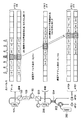
図11はBB84プロトコルによる量子暗号鍵配布方法の概念を示す模式図である。ここではAlice141とBob143とが光伝送路142で接続されているものとする。
FIG. 11 is a schematic diagram showing the concept of a quantum key distribution method based on the BB84 protocol. Here, it is assumed that Alice 141 and Bob 143 are connected by an
この方法では、Alice141が乱数源を2つ持ち、片側(乱数1)で0/1の暗号鍵データを表し、もう一方(乱数2)で乱数1の情報をコーディングする方法を決定する。光子の位相を利用した量子暗号鍵配布方法では、位相0が暗号鍵“0”、位相πが暗号鍵“1”の組を表すコーディングセット(以下、「+基底」と称する。)と、位相π/2が暗号鍵“0”、位相3π/2が暗号鍵“1”を表すコーディングセット(以下、「×基底」と称する。)と、の2組の基底を乱数2で選択する。つまり1つの光子に対して、0、π/2、π、3π/2の4通りの変調をランダムに施してBobへと送信する。
In this method, Alice 141 has two random number sources, one side (random number 1) represents 0/1 encryption key data, and the other (random number 2) determines how to code
一方、Bob143では基底に対応する乱数源(乱数3)を持ち、Alice141より送られてきた光子に対してデコードを行う。乱数3の値が“0”である場合、光子に対して位相0(+基底)の変調を、“1”である時には位相π/2(×基底)の変調を施す。ここで光学干渉計出力として得られた乱数を乱数4とする。
On the other hand, Bob 143 has a random number source (random number 3) corresponding to the base, and decodes photons sent from Alice 141. When the value of the
Alice/Bob両者が施した変調の基底が同一である場合(乱数2=乱数3)、乱数1の値をBobは正しく検出することができ(乱数1=乱数4)、異なる場合(乱数2≠乱数3)には乱数1の値に依らずBobは乱数4として0/1の値をランダムに得る。乱数1/2/3は共に1ビット毎に変化する乱数であるから、基底が一致する確率と不一致である確率は共に50%となるが、後段の基底照合(Basis Reconciliation)によって基底が不一致となるビットを削除するから、Alice141とBob143は乱数1に対応する0/1ビット列を共有することができる。
When the basis of modulation performed by both Alice / Bob is the same (
しかしながら、上記のようにして共有したビット列には伝送路142や受信器に起因する誤りが含まれており、この誤りを訂正する誤り訂正処理が必要となる。加えて伝送路途中に存在する盗聴者が光子情報を覗き見た場合にも共有ビット列に誤りが発生する。したがって、最終的に使用する暗号鍵を共有するためには、誤りを訂正する誤り訂正処理だけでなく、誤りの頻度(誤り率)に基づいて、盗聴されたと想定し得る情報量を削減する秘匿増強処理が必要となる。なお「盗聴されたと想定し得る情報量」を推定する方法は、非特許文献2および3に記載されている。
However, the bit strings shared as described above include errors due to the
図12は、一般的な量子暗号鍵生成の流れを示すフローチャートである。Aliceより送られた暗号鍵の元乱数(鍵の素)は、量子暗号鍵配布(単一光子伝送)S1によって大部分の情報量が失われる。この段階でAliceとBobで共有されている鍵を生鍵(Raw Key)と呼び、上述した基底照合S2を行った後で半減した暗号鍵を選別鍵(Sifted Key)と呼ぶ。この後、量子鍵配布段階で混入した誤りを訂正する誤り訂正(Error Correction)S3過程と、盗聴者に漏れていると想定され得る情報量を削ぎ落とす秘匿増強(Privacy Amplification)S4とを経て、残りが実際に暗号鍵として使用される最終鍵となる。このような量子暗号鍵を共有する技術がいくつか提案されている。 FIG. 12 is a flowchart showing a general flow of quantum key generation. Most of the information amount of the original random number (key element) of the encryption key sent from Alice is lost by the quantum encryption key distribution (single photon transmission) S1. At this stage, a key shared by Alice and Bob is called a raw key, and an encryption key halved after performing the above-described base collation S2 is called a selection key. After this, an error correction S3 process for correcting an error mixed in the quantum key distribution stage and a privacy amplification S4 for cutting off the amount of information that can be assumed to be leaked to an eavesdropper, The rest is the final key that is actually used as the encryption key. Several techniques for sharing such quantum encryption keys have been proposed.
たとえば、特開2000−174747号公報(特許文献1)には、量子チャネルと古典チャネルとを用いて送信側および受信側で秘密鍵を共有する量子暗号装置が開示されている。具体的には、送信者側で乱数表からビット値を取り出し、それに従って光パルスを微小変調し、量子チャネルを通して送信する。受信者側は、別途乱数表からビット値を取り出し、それに従って受信した光パルスを再変調し、光子が検出されたか否かを古典チャネルを通して送信者側へ通知する。送信者側では、受信者側で光子が検出されたビット値のみを用いて乱数表を構成する。これによって、送信者および受信者に共通の乱数表が記憶されたこととなる。さらに、盗聴の有無を確認するために、共通乱数表から適当な割合で照合ビットを抽出し、それらを古典チャネルを通して照合し、十分な数のビットが一致すれば、照合ビットを除いたビット列を共有の秘密鍵として使用する(明細書段落0036〜0039参照)。 For example, Japanese Patent Laid-Open No. 2000-174747 (Patent Document 1) discloses a quantum cryptography device that uses a quantum channel and a classical channel to share a secret key on the transmission side and the reception side. Specifically, the bit value is extracted from the random number table on the transmitter side, the optical pulse is minutely modulated according to the bit value, and transmitted through the quantum channel. The receiver side separately extracts the bit value from the random number table, remodulates the received optical pulse accordingly, and notifies the transmitter side through the classical channel whether or not a photon has been detected. On the sender side, a random number table is constructed using only the bit values for which photons are detected on the receiver side. As a result, a random number table common to the sender and the receiver is stored. Furthermore, in order to confirm the presence / absence of eavesdropping, collation bits are extracted from the common random number table at an appropriate ratio, collated through the classical channel, and if a sufficient number of bits match, a bit string excluding the collation bits is obtained. Used as a shared secret key (see specification paragraphs 0036-0039).
特開2004−112278号公報(特許文献2)には、量子通信路(量子チャネル)を通ることによって発生するデータ誤りを除去することで、共通鍵の生成効率を向上させる量子鍵配送方法が開示されている。より詳しくは、送信側は、乱数列(送信データ)およびランダムに決定された基底(送信コード)により規定された量子状態で光子を量子通信路を通して送信する。受信側では、受信した光子を測定し、その測定結果とランダムに決定された基底(受信コード)とにより規定された受信データを得る。そして、公開通信路を通した手順で基底の一致したビットのみを残すことで、送信側および受信側に共有情報が記憶される。続いて、送信側はパリティ検査行列および送信データから生成される所定ビット数の誤り訂正情報を公開通信路を通して送信する。受信側は、受信した誤り訂正情報、上記受信データおよび同一のパリティ検査行列を用いて、受信データの誤りを訂正する。誤り訂正で公開された情報に応じて、訂正後の共有情報の一部が捨てられ、残りの情報を共有の暗号鍵として生成する(明細書段落0016〜0020、図1、図2、図9参照)。 Japanese Unexamined Patent Application Publication No. 2004-112278 (Patent Document 2) discloses a quantum key distribution method that improves common key generation efficiency by removing data errors that occur when passing through a quantum communication channel (quantum channel). Has been. More specifically, the transmission side transmits photons through a quantum communication channel in a quantum state defined by a random number sequence (transmission data) and a randomly determined basis (transmission code). On the receiving side, the received photons are measured, and reception data defined by the measurement result and a randomly determined base (reception code) is obtained. Then, the shared information is stored on the transmission side and the reception side by leaving only the bits whose bases match in the procedure through the public communication path. Subsequently, the transmission side transmits error correction information of a predetermined number of bits generated from the parity check matrix and the transmission data through the public communication path. The receiving side corrects errors in the received data using the received error correction information, the received data, and the same parity check matrix. Depending on the information disclosed by error correction, a part of the corrected shared information is discarded, and the remaining information is generated as a shared encryption key (specifications paragraphs 0016 to 0020, FIGS. 1, 2, and 9). reference).
しかしながら、上述した量子暗号鍵配布を現実世界で実現しようとすると、様々な原因によって上記誤り率が上昇することがある。具体的には、単一光子に情報を載せて伝送するので伝送路途中で消失するビットが多く、Alice−Bob間でのビット対応の誤認識が生じやすい。この誤認識によって誤り率が劣化し、暗号鍵の生成が行えなくなる。以下、送信側と受信側との間でビット位置の同期が取れていること、すなわちビット対応の正しい認識が成立している状態を「フレーム同期」、ビット対応が誤認識されている状態を「フレーム同期ずれ」、フレーム同期ずれをフレーム同期状態に正しく合わせる処理を「フレーム同期処理」と称す。 However, if the above-described quantum cipher key distribution is to be realized in the real world, the error rate may increase due to various causes. Specifically, since information is carried on a single photon and transmitted, there are many bits that disappear in the middle of the transmission path, and misrecognition of bit correspondence between Alice and Bob tends to occur. This misrecognition degrades the error rate and makes it impossible to generate an encryption key. Hereinafter, the bit position is synchronized between the transmitting side and the receiving side, that is, the state where correct recognition of bit correspondence is established is `` frame synchronization '', and the state where bit correspondence is erroneously recognized is `` The process of correctly matching the frame synchronization deviation with the frame synchronization state is referred to as “frame synchronization processing”.
上述したように、送信側と受信側で情報を共有するためには、どのビットが正しく検出され、どのビットが検出されなかったかを、送信器および受信器の双方で特定できなければならない。言い換えれば、量子暗号鍵配布システムでは送信器と受信器とでビット位置の同期を確立することが必要である。鍵生成フローにおいて、ビット位置の同期確立は大前提であり、同期が確立していないと最終鍵は生成できない。 As described above, in order to share information between the transmission side and the reception side, it is necessary to be able to specify which bits are correctly detected and which bits are not detected in both the transmitter and the receiver. In other words, in the quantum key distribution system, it is necessary to establish bit position synchronization between the transmitter and the receiver. In the key generation flow, establishment of synchronization of bit positions is a major premise, and the final key cannot be generated unless synchronization is established.
しかしながら、上記従来の方法では、伝送路の伸縮や装置内の処理のずれによって、フレーム同期が外れる可能性が残されている。実際の運用において同期がはずれた場合、特許文献1に記載された鍵生成フローでは、照合ビットが十分一致しないために、盗聴者を検出したとみなし、再度ビット位置の同期を確立し直して鍵生成を実行することとなる。これでは、それまでに量子通信で生成した鍵は無駄となり、共通鍵の生成効率がきわめて悪くなる。同様に、特許文献2に記載された方法においても、ビット位置の同期が外れた場合には受信データの誤り率が非常に大きくなり、共通鍵を生成できなくなる。特許文献2では、誤り率が大きい場合の処理については全く考慮されていない。
However, in the above-described conventional method, there is a possibility that frame synchronization is lost due to expansion / contraction of the transmission path or a shift in processing in the apparatus. When synchronization is lost in actual operation, the key generation flow described in
特に、本発明者等は、フレーム同期ずれの原因が伝送路の伸縮などの装置間の処理ずれだけでなく受信器側の装置内の処理ずれも関係していることに注目し、正確なフレーム同期を迅速に確立する同期制御方法を提案する。 In particular, the present inventors have noted that the cause of the frame synchronization deviation is related not only to the processing deviation between devices such as expansion and contraction of the transmission path but also to the processing deviation in the device on the receiver side, A synchronization control method to quickly establish synchronization is proposed.
上記目的を達成するために、本発明によれば、複数の通信チャネルにより接続された第1通信器と第2通信器との間で共有すべきデータのビット対応を確立する同期制御方法において、a)前記第1通信器は、それぞれビットタイミングが相対的に定められた複数のビット列からなる第1データを一の通信チャネルを通して前記第2通信器へ送信し、前記第2通信器は前記一の通信チャネルを通して前記第1通信器から受信した第2データを保存し、b)前記第1通信器と前記第2通信器との間のビットタイミング差である第1同期ずれと、前記第2通信器内のビットタイミング差である第2同期ずれと、を仮設定し、c)仮設定された前記第1同期ずれおよび前記第2同期ずれを所定調整範囲内で順次変更しながら、前記第2データの一部とそれに対応する前記第1データとを照合し、d)前記照合結果に基づいて前記第1同期ずれおよび前記第2同期ずれを確定する、ことを特徴とする。 To achieve the above object, according to the present invention, in a synchronization control method for establishing bit correspondence of data to be shared between a first communication device and a second communication device connected by a plurality of communication channels, a) The first communication device transmits first data composed of a plurality of bit strings, each of which has a relatively determined bit timing, to the second communication device through one communication channel, and the second communication device transmits the first communication device to the first communication device. B) storing the second data received from the first communication device through the communication channel, b) a first synchronization shift that is a bit timing difference between the first communication device and the second communication device, and the second data A second synchronization shift that is a bit timing difference in the communication device, and c) the first synchronization shift and the second synchronization shift that are temporarily set within a predetermined adjustment range while sequentially changing the first synchronization shift and the second synchronization shift. Part of 2 data Collating the first data corresponding thereto, to determine the first synchronization deviation and the second sync deviation based on d) the comparison result, characterized in that.
本発明の一実施例によれば、前記c)は、c.1)仮設定された前記第1同期ずれおよび仮設定された前記第2同期ずれを用いて、前記第2データの一部のビットタイミングにそれぞれ対応する前記第1データのビットタイミングを決定し、c.2)前記第2データの前記一部の値とそれらに対応する前記第1データの値とを照合し、c.3)仮設定された前記第1同期ずれおよび仮設定された前記第2同期ずれの少なくとも一方を所定ステップ変化させ、c.4)前記c.1)〜c.3)を前記所定調整範囲内で繰り返す。前記d)は、前記照合結果のうち最も良好な照合結果をもたらす仮設定された第1同期ずれおよび第2同期ずれを同期確立された前記第1同期ずれおよび前記第2同期ずれとして決定する。 According to one embodiment of the present invention, said c) comprises c. 1) Using the temporarily set first synchronization shift and the temporarily set second synchronization shift, determine bit timings of the first data respectively corresponding to partial bit timings of the second data; c. 2) collating the partial values of the second data with the corresponding values of the first data; c. 3) Change at least one of the temporarily set first synchronization deviation and the temporarily set second synchronization deviation by a predetermined step, c. 4) c. 1) to c. 3) is repeated within the predetermined adjustment range. In the step d), the temporarily set first synchronization error and second synchronization error that produce the best verification result among the verification results are determined as the first synchronization error and the second synchronization error that have been established in synchronization.
本発明の他の実施例によれば、前記c)は、c.1)仮設定された前記第1同期ずれおよび仮設定された前記第2同期ずれを用いて、前記第2データの一部のビットタイミングにそれぞれ対応する前記第1データのビットタイミングを決定し、c.2)前記第2データの前記一部の値とそれらに対応する前記第1データの値とを照合し、c.3)前記照合結果が所定の閾値より良好でない場合には、仮設定された前記第1同期ずれおよび仮設定された前記第2同期ずれの少なくとも一方を所定ステップ変化させ、c.4)前記c.1)〜c.3)を前記所定調整範囲内で繰り返し、前記d)は、前記c.2)で得られた前記照合結果が前記所定の閾値より良好である場合には、当該照合結果をもたらす仮設定された第1同期ずれおよび第2同期ずれを同期確立された前記第1同期ずれおよび前記第2同期ずれとして決定する。 According to another embodiment of the present invention, said c) comprises c. 1) Using the temporarily set first synchronization shift and the temporarily set second synchronization shift, determine bit timings of the first data respectively corresponding to partial bit timings of the second data; c. 2) collating the partial values of the second data with the corresponding values of the first data; c. 3) If the collation result is not better than a predetermined threshold value, change at least one of the temporarily set first synchronization shift and the temporarily set second synchronization shift by a predetermined step; c. 4) c. 1) to c. 3) is repeated within the predetermined adjustment range, and d) If the collation result obtained in 2) is better than the predetermined threshold value, the first synchronization deviation and the first synchronization deviation, which are temporarily set to produce the collation result, are synchronized with each other. And the second synchronization shift is determined.
本発明の更に別の実施例によれば、前記c)およびd)は、e.1)仮設定された前記第1同期ずれおよび仮設定された前記第2同期ずれを用いて、前記第2データの一部のビットタイミングにそれぞれ対応する前記第1データのビットタイミングを決定し、e.2)前記第2データの前記一部の値とそれらに対応する前記第1データの値とを照合し、e.3)前記照合結果が第1閾値より良好でない場合には、仮設定された前記第1同期ずれを所定ステップ変化させ、e.4)前記e.1)〜e.3)を前記第1同期ずれの所定調整範囲内で繰り返し、e.5)前記e.2)で得られた前記照合結果が前記第1閾値より良好である場合には、当該照合結果をもたらす仮設定された第1同期ずれを同期確立された前記第1同期ずれとして決定し、e.6)前記e.2)で得られた前記照合結果が前記第1閾値より良好で、かつ、第2閾値より良好でない場合には、仮設定された前記第2同期ずれを所定ステップ変化させ、e.7)前記第2データの前記一部の値とそれらに対応する前記第1データの値とを照合し、e.8)前記e.7)で得られた前記照合結果が前記第2閾値より良好でない場合には、前記e.6)〜e.7)を前記第2同期ずれの所定調整範囲内で繰り返し、e.9)前記e.7)で得られた前記照合結果が前記第2閾値より良好である場合には、当該照合結果をもたらす仮設定された第2同期ずれを同期確立された前記第2同期ずれとして決定する。 According to yet another embodiment of the present invention, said c) and d) are: e. 1) Using the temporarily set first synchronization shift and the temporarily set second synchronization shift, determine bit timings of the first data respectively corresponding to partial bit timings of the second data; e. 2) collating the partial values of the second data with the corresponding values of the first data; e. 3) If the collation result is not better than the first threshold value, change the temporarily set first synchronization shift by a predetermined step; e. 4) The e. 1) to e. 3) is repeated within a predetermined adjustment range of the first synchronization shift, e. 5) said e. If the collation result obtained in 2) is better than the first threshold value, the temporarily set first synchronization deviation that causes the collation result is determined as the first synchronization deviation that has been established, and e . 6) said e. If the collation result obtained in 2) is better than the first threshold and not better than the second threshold, the temporarily set second synchronization shift is changed by a predetermined step; e. 7) collating the partial value of the second data with the corresponding value of the first data; e. 8) said e. When the collation result obtained in 7) is not better than the second threshold value, the e. 6) to e. 7) is repeated within a predetermined adjustment range of the second synchronization shift, e. 9) e. When the collation result obtained in 7) is better than the second threshold value, the temporarily set second synchronization deviation that causes the collation result is determined as the second synchronization deviation that has been established.
本発明によれば、第1同期ずれおよび第2同期ずれを所定調整範囲内で順次変更しながら、受信側の第2データの一部とそれに対応する送信側の第1データとを照合し、その照合結果に基づいて第1同期ずれおよび第2同期ずれを確定する。したがって、第1通信器および第2通信器の間の処理ずれだけでなく第2通信器内の処理ずれも考慮するので、正確なフレーム同期を迅速に確立することができ、安定した信頼性の高い通信システムを実現できる。 According to the present invention, while sequentially changing the first synchronization deviation and the second synchronization deviation within a predetermined adjustment range, a part of the second data on the reception side and the corresponding first data on the transmission side are collated, Based on the collation result, the first synchronization deviation and the second synchronization deviation are determined. Therefore, since not only the processing shift between the first communication device and the second communication device but also the processing shift in the second communication device is taken into account, accurate frame synchronization can be quickly established, and stable and reliable. A high communication system can be realized.
特に、本発明を量子暗号鍵配布システムに適用した場合、暗号鍵の生成を安定して行うことができる。従来の量子暗号鍵配布技術では誤り率(QBER)の劣化は盗聴者の存在を意味していたが、本発明では暗号鍵生成を中断する前に復旧処理を施すことができ、環境変化や通信エラー等に起因する誤り率劣化を盗聴行為の存在と誤認識することが無くなる。従って従来であれば鍵生成を中断していたところが、暗号鍵の生成を再開することができるので暗号鍵生成の長時間に渡る安定動作を実現できる。 In particular, when the present invention is applied to a quantum cryptographic key distribution system, cryptographic key generation can be performed stably. In the conventional quantum encryption key distribution technology, the deterioration of the error rate (QBER) means the presence of an eavesdropper. However, in the present invention, recovery processing can be performed before interrupting the generation of the encryption key, and environmental changes and communication can be performed. An error rate deterioration caused by an error or the like is not erroneously recognized as the presence of an eavesdropping action. Therefore, in the past, the key generation was interrupted, but the generation of the encryption key can be resumed, so that a stable operation over a long period of time can be realized.
本発明は、送信側および受信側でデータの同期を必要とする通信システムに広く適用可能であるが、その望ましい実施形態として、ここでは量子暗号鍵配布システムについて説明する。特にPlug&Play方式は、光ファイバ伝送路における偏光の揺らぎを補償することができるため、偏光に敏感な量子暗号鍵配布システムを実用化するための方式として期待されている(非特許文献4および6を参照)。
The present invention can be widely applied to communication systems that require data synchronization on the transmission side and the reception side. As a preferred embodiment, a quantum key distribution system will be described here. In particular, the Plug & Play method can compensate for fluctuations in polarization in an optical fiber transmission line, and thus is expected as a method for putting a quantum cryptographic key distribution system sensitive to polarization into practical use (see
1.システム構成
図1は本発明の一実施形態によるPlug&Play方式の量子暗号鍵配布システムの構成を示すブロック図である。本実施形態による量子暗号鍵配布システムでは、送信器(Alice)10と受信器(Bob)20とが光ファイバ伝送路30を介して接続されている。
1. System Configuration FIG. 1 is a block diagram showing the configuration of a plug & play quantum key distribution system according to an embodiment of the present invention. In the quantum key distribution system according to the present embodiment, a transmitter (Alice) 10 and a receiver (Bob) 20 are connected via an optical
1.1)送信器(Alice)
送信器10の量子ユニットは、位相変調器101および偏光ビームスプリッタ(PBS)102から構成されるPBSループと可変光減衰器103とを有する。位相変調器101は、位相制御部104から供給される位相制御信号に従って、通過する光パルス列に対して位相変調を行う。位相変調の深さは、ここでは基底(+/×)を示す乱数および鍵の素データを示す乱数(0/1)の4通りの組み合わせにそれぞれ対応する4通りの深さ(0、π/2、π、3π/2)となる。位相制御信号は変調の深さに対応した電圧であり、光パルスが位相変調器101を通過するタイミングで位相変調器101に印加され、当該光パルスの位相変調が行われる。位相制御部104は、光受信器105により受信した同期クロックに従って位相制御信号を位相変調器101へ印加するが、後述するように、その印加タイミングと印加電圧は制御部107により制御される。
1.1) Transmitter (Alice)
The quantum unit of the
PBSループはファラデーミラーと同様の機能を有し、PBS102に受信器側から入射した光の偏光状態が90度回転して送出される(詳しくは、本出願人により平成16年11月19日に出願された特願2004−335228号の明細書、非特許文献7を参照)。受信器20から入射した量子ユニットの光信号は、光可変減衰器103を通してPBSループで上述したように折り返され、光可変減衰器103を通して受信器20へ送出される。光可変減衰器103は、量子ユニットの同期を取るためのトレーニングモード時には小さい減衰量に設定され、鍵生成のための量子モード時には単一光子伝送となるように大きい減衰量に設定される。
The PBS loop has the same function as the Faraday mirror, and the polarization state of the light incident on the
また、送信器10は2個の乱数発生器(図示せず)を有し、制御部107は一方の乱数発生器で暗号鍵の素データ(0/1)を、もう一方の乱数発生器で基底情報(+/×)をそれぞれ生成してメモリ109に順次格納する。後述するように、格納された乱数のビット番号はメモリ109のアドレスを用いて管理される。メモリ109としては、高速アクセスが実現できるメモリが望ましく、ここではSDRAMを使用する。
Further, the
鍵生成フローが開始されると、制御部107は光可変減衰器103の減衰量を大きくし、メモリ109から素データおよび基底を1組ずつ順次読み出して位相制御部104へ出力する。位相制御部104は、素データおよび基底の組に対応した位相制御信号を同期クロックに従って位相変調器101へ出力することで、位相変調器101を通過する光パルスに対して4通りの深さ(0、π/2、π、3π/2)の変調が施される。
When the key generation flow is started, the
位相制御部104に供給される同期クロックは、受信器20から光ファイバ伝送路30を通して受信した基準クロックを用いる。基準クロックは光受信器105により電気信号に変換され位相制御部104へ出力される。同時に、この基準クロックは光送信器106へも出力され、基準クロックとして受信器20へ折り返される。また、制御部107は、光送受信器108を通して鍵生成、同期処理や補正処理などに必要なデータおよび制御信号を受信器20の制御部211との間でやり取りする。
The reference clock received from the
本実施形態では波長分割多重伝送が用いられ、量子ユニットの通信、基準クロックの送受信および制御部107のデータ通信は、それぞれ異なる波長により行われる。送信器10には波長合分波器110が設けられ、光ファイバ伝送路30から入射した光信号を分波して、光可変減衰器103、光受信器105および光送受信器108へ出力し、逆に、光可変減衰器103、光送信器106および光送受信器108から出射した光信号を合波して光ファイバ伝送路30へ送出する。すなわち、光ファイバ伝送路30には、量子ユニットで使用される量子チャネルと、光受信器105、光送信器106および光送受信器108でそれぞれ使用される古典チャネルとが波長多重されている。
In this embodiment, wavelength division multiplexing transmission is used, and communication of the quantum unit, transmission / reception of the reference clock, and data communication of the
1.2)受信器(Bob)
本実施形態における受信器20の量子ユニットは、光サーキュレータ203、光カプラ204、位相変調器205、PBS206および光検出器APD0、APD1を有する。光カプラ204とPBS206の間には長いパスと短いパスが並列に設けられている。位相変調器205は長いパスに設けられ、位相制御部210からの位相制御信号により位相変調の深さ(基底)と駆動タイミングとが制御される。光検出器APD0およびAPD1はアバランシェ・フォトダイオード(APD)であり、位相制御部210からの制御信号によりガイガーモード(Gated Geiger Mode)で駆動される(非特許文献5を参照)。
1.2) Receiver (Bob)
The quantum unit of the
受信器20には基準クロック源201が設けられ、レーザ源202は基準クロック源201により生成された基準クロックに従って駆動され、同時に、その基準クロックは光送信器208を通して送信器10へ送出される。送信器10では、その基準クロックを用いて同期タイミングを決定すると共に、その基準クロックをそのまま受信器20へ折り返す。送信器10から折り返された基準クロックは光受信器209によって受信され、受信器20の同期クロックとして位相制御部210へ供給される。位相制御部210は、制御部211の制御の下で、供給された基準クロックに同期するように位相変調器205の位相変調の深さおよび電圧印加タイミングを制御し、光検出器APD0およびAPD1に光子検出のための逆バイアス電圧の印加タイミングを制御する。
The
また、受信器20は1個の乱数発生器(図示せず)を有し、制御部211は乱数発生器で基底情報(+/×)を生成してメモリ214に順次格納する。鍵生成フローが開始されると、制御部211はメモリ214から基底情報を順次読み出し、位相制御部210へ出力する。メモリ214には、高速アクセスが実現できるメモリが使用される(ここではSDRAM)。位相制御部210は、基準クロックに従って位相変調器205に対して当該基底に対応する電圧の位相制御信号を印加する。これによって、送信器10から伝送されてきた光パルスが位相変調器205を通過するタイミングに合わせて当該基底に対応した変調を施すことができる。
Further, the
後述するように送信器10の位相変調器101で変調された光パルスと受信器20の位相変調器205で変調された光パルスとが光カプラ204で干渉し、それぞれの位相変調の深さの差に応じて光検出器APD0あるいは光検出器APD1で光子が検出される。光検出器APD0およびAPD1のそれぞれの検出信号は生鍵として順次メモリ213に書き込まれる。なお、メモリ213に書き込まれる生鍵のビット番号およびメモリ214に格納される基底情報としての乱数のビット番号は、後述するようにそれぞれのメモリのアドレスを用いて管理される。メモリ213として、ここでは高速アクセスが実現できるSDRAMを使用する。また、メモリ213および214は同一メモリの別領域であってもよい。
As will be described later, the optical pulse modulated by the
続いて、メモリ213に格納された生鍵のビット番号とそれらに対応するメモリ214に格納された基底情報とを送信器10の制御部107へ通知し、上述した基底照合を経て基底が不一致の乱数ビットが捨てられるが、その際、基底が一致したビットのうちメモリ109に格納された素データとメモリ213に格納された検出データとの一致/不一致も検出され、誤り率QBERが算出される。モニタ212は誤り率QBERをメモリ213に蓄積しつつQBERの変化を常時監視し、制御部211は誤り率QBERの値あるいはその変化量に応じて、後述する位相補正処理あるいはフレーム同期処理を適宜実行する。
Subsequently, the bit numbers of the raw keys stored in the
上述したように本実施形態では波長分割多重伝送が用いられ、量子ユニットの通信、基準クロックの送受信および制御部211の基底照合等のデータ通信は、それぞれ異なる波長により行われる。受信器20には波長合分波器207が設けられ、光ファイバ伝送路30から入射した光信号を分波してPBS206、光受信器209および光送受信器215へ出力し、逆に、PBS206、光送信器208および光送受信器215から出射した光信号を合波して光ファイバ伝送路30へ送出する。
As described above, wavelength division multiplexing transmission is used in this embodiment, and data communication such as quantum unit communication, reference clock transmission / reception, and base verification of the
2.システム動作
基準クロック源201から供給されるクロック信号に従ってレーザ源202から出射した光パルスPは、光サーキュレータ203により光カプラ204へ導かれ、光カプラ204により2分割される。分割された一方の光パルスP1は短いパスを通って直接PBS206へ送られ、分割された他方の光パルスP2は長いパスに設けられた位相変調器205を通してPBS206へ送られる。これら光パルスP1およびP2はPBS206で合波され、ダブルパルスとして波長合分波器207および光伝送路30を通して送信器10へ送信される。
2. System Operation The optical pulse P emitted from the
送信器10において、伝送路30から波長合分波器110および可変光減衰器103を通して到来したダブルパルスP1およびP2は、PBS102でさらに分離され、時計回りのダブルパルスP1CWおよびP2CWと反時計回りのダブルパルスP1CCWおよびP2CCWの4つのパルス、すなわちカルテットパルスとなって位相変調器101をそれぞれ反対方向で通過し、それぞれ出射したポートとは反対のPBSポートへ入射する。
In the
位相変調器101は、時計回りのダブルパルスの後方のパルスP2CWを前方のパルスP1CWに対して位相変調するとともに、反時計回りのダブルパルスと時計回りのダブルパルスとの間にπの位相差を与える。位相変調器101は位相制御部104の位相制御信号によってカルテットパルスの各パルスに任意の位相変調を施すようにタイミング制御される。
The
こうして必要に応じて位相変調されたカルテットパルスはPBS102で合波され再びダブルパルスに戻る。上述したように後方のパルスのみが伝送情報により位相変調されたので、出射ダブルパルスをP1およびP2*aと記す。このときPBSループ入射時に対して出射時は偏波が90°回転しているので、結果的にファラデーミラーと同等の効果が得られる。
Thus, the quartet pulses that are phase-modulated as necessary are combined by the
受信器20のPBS206は、送信器10から受信した光パルスP1およびP2*aの偏光状態が90度回転していることから、これら受信パルスをそれぞれ送信時とは異なるパスへ導く。すなわち受信した光パルスP1は長いパスを通り、位相変調器205を通過するタイミングで指定された基底で位相変調され、位相変調された光パルスP1*bが光カプラ204に到達し、他方、光パルスP2*aは送信時とは異なる短いパスを通って同じく光カプラ204に到達する。
The
こうして送信器10で位相変調された光パルスP2*aと受信器20で位相変調された光パルスP1*bとが干渉し、その結果が光子検出器APD0またはAPD1により検出される。光子検出器APD0およびAPD1は、位相制御部210から供給されるクロック信号に従ってガイガーモードで駆動され、その検出データはメモリ213に順次格納される。そして基底照合の際に算出されたQBERがモニタ212により監視され、制御部211は、誤り率QBERと予め格納された閾値とを比較しながら、必要に応じてフレーム同期の復旧処理を実行する。以下、本発明の望ましい実施例によるフレーム同期制御方法について詳細に説明する。これら実施例によるフレーム同期制御方法は、送信器10の制御部107と受信器20の制御部211およびモニタ212とによって実行されるが、送信器10および受信器20のそれぞれのプログラム制御プロセッサ上でフレーム同期制御プログラムを実行することで同様の機能を実現してもよい。
Thus, the optical pulse P2 * a phase-modulated by the
1.1)装置間および装置内の処理ずれの定義
図2は、量子暗号鍵配布システムにおける装置間および装置内の伝搬遅延によりビット番号がずれる様子を示した模式図である。上述したように、データおよび基底のビット番号はメモリのアドレスにより管理される。
1.1) Definition of Processing Deviation Between Devices and Within Device FIG. 2 is a schematic diagram showing how bit numbers shift due to propagation delays between devices and within devices in a quantum key distribution system. As described above, data and base bit numbers are managed by memory addresses.
送信器10のメモリ109には、暗号鍵の素データの乱数がアドレス( … i-3, i-2, i-1, i, i+1,…)に、基底情報の乱数がアドレス( … j-3, j-2, j-1, j, j+1,…)にそれぞれ格納され、iとjとが対応しているものとする。位相変調器101によって変調を施す時、制御部107はメモリ109のアドレスi,jからそれぞれデータおよび基底を読み出し、その組み合わせに対応した変調の深さで位相変調器101により光パルスの位相変調が行われる。ただし、装置内の等遅延設計により、アドレスiおよびjからの読み出しには遅延差がなく、i=jを常に満たすものと仮定する。
In the
送信器10から送出されたダブルパルスは、上述したように受信器20のPBS206で受信器20を出射したときは別のパスに導かれ、一方は短いパスを通してそのまま光カプラ204へ、他方は長いパスを通して位相変調器205で位相変調され光カプラ204へ到達する。位相変調器205によって変調を施す時、制御部211はメモリ214のアドレス(k)から基底を読み出し、それに対応した変調の深さで位相変調器205が光パルスに位相変調を行う。
The double pulse transmitted from the
こうして光検出器APD0およびAPD1により検出されたデータはメモリ213のアドレスl(エル),mに順次書き込まれる。この場合も装置内の等遅延設計により、アドレスlおよびmへの書き込みには遅延差がなく、l=mを常に満たすものと仮定する。
Thus, the data detected by the photodetectors APD0 and APD1 are sequentially written to the addresses l (el) and m of the
このように、送信器10におけるメモリ109の読み出しアドレスi,j、受信器20におけるメモリ214の読み出しアドレスkおよびメモリ213の書き込みアドレスl,mは全て異なる値となるが、送信側のどのビットが受信側のどのビットに対応するかを正しく認識するためには、これらのメモリの間でアドレスの対応関係を決定しておく必要がある。
As described above, the read address i and j of the
そこで、i=jおよびl=mが常に満たされるとして、送信器10のメモリ109の変調アドレスと受信器20のメモリ213の検出アドレスとの差を装置間アドレス差分GD(= l - i)、受信器20の内部での変調アドレスと検出アドレスとの差を装置内アドレス差分GI(= l - k)と呼ぶ。
Therefore, assuming that i = j and l = m are always satisfied, the difference between the modulation address of the
1.2)フレーム同期ずれとQBER劣化
装置間アドレス差分GDおよび/または装置内アドレス差分GIが温度変化等の原因で変動すると、QBERは次のように変動する。なお、簡単の為にAliceから送信したビットは全てBobに誤り無く届くと仮定する。
1.2) If the inter-frame synchronization deviation and QBER deterioration device address difference G D and / or device address difference G I varies due to temperature change or the like, QBER varies as follows. For simplicity, it is assumed that all bits transmitted from Alice reach Bob without error.
a)GD, GI共に正しい場合
図3は、装置間アドレス差分GDと装置内アドレス差分GIとが共に正しい場合のビット対応を示す模式図である。QBERの計算では、Alice及びBobにおいて施した変調の基底(Basis)が一致するビットに関してデータの一致率を計算する。図4に示す様に、基底の一致しないビットに関しては誤り率に影響せず、基底の一致したビットではAlice側のデータAとBob側のデータBとは一致するので、QBERは0%となる。
a) G D, G I both correct if Figure 3 is a schematic diagram showing a bit correspondence in the case with the inter-device address difference G D and device address difference G I are both correct. In the calculation of QBER, the data coincidence rate is calculated for the bits having the same basis of the modulation applied in Alice and Bob. As shown in FIG. 4, the error rate is not affected for bits whose bases do not match, and the data Alice on the Alice side and the data B on the Bob side match for the bits whose bases match, so the QBER is 0%. .
b)GDが正しくない場合
図4は、装置間アドレス差分GDが正しくない場合のビット対応を示す模式図である。この場合には、基底照合の際に比較するビットが異なるので相関の無い乱数をずらして比較することとなり、QBERは約50%となる。しかしながら、QBERを計算する際のビット量によって、フレーム同期ずれが計算範囲の途中で生じたり計算結果そのもののばらつき等も生じたりする。したがって、これらも考慮してQBER計算結果が30%〜60%程度の範囲内であれば、GDが正しくない場合のフレーム同期ずれが生じていると判断できる。このGD不正フレーム同期ずれを判定する基準として、装置間フレーム同期ずれ閾値Qbitを30%〜60%の範囲内に設定する。
If b) G D is incorrect Figure 4 is a schematic diagram showing a bit to do if the inter-device address difference G D is incorrect. In this case, since the bits to be compared in the base collation are different, random numbers having no correlation are shifted and compared, and the QBER is about 50%. However, depending on the amount of bits when calculating the QBER, a frame synchronization shift may occur in the middle of the calculation range or the calculation result itself may vary. Therefore, it can be determined that if these also within the scope and QBER calculation result is approximately 30% to 60% taking into account, the frame synchronization deviation in the case G D is incorrect has occurred. As criteria for determining the G D abnormal frame synchronization deviation, sets the threshold value Q bit shift device between frame synchronization within the range of 30% to 60%.
c)GIが正しくない場合
図5(A)は装置内アドレス差分GIが正しくない場合のビット対応を示す模式図であり、(B)はこの場合のQBERの推定範囲を説明するための図である。この場合には、図5(A)に示すように、Bob内部で変調のための基底情報アドレスと検出信号の書き込みアドレスとがずれている。したがって、QBER計算は上記(a)、(b)の様に単純ではなく、図5(B)の様な場合分けで考える必要がある。
c) Figure If G I is incorrect. 5 (A) is a schematic diagram showing a bit enabled when device address difference G I is incorrect, (B) is for illustrating the estimation range of QBER in this case FIG. In this case, as shown in FIG. 5A, the base information address for modulation and the write address of the detection signal are shifted inside Bob. Therefore, the QBER calculation is not as simple as the above (a) and (b), and it is necessary to consider the case classification as shown in FIG.
まず、Aliceにおいてiビット目で変調された光子が、Bobにおいて(i+1)ビット目で変調され、iビット目で受信されたと仮定する。但し、Bobはiビット目で変調したものと誤認している。 First, it is assumed that a photon modulated at the i-th bit in Alice is modulated at the (i + 1) -th bit and received at the i-th bit in Bob. However, Bob misunderstands that it is modulated at the i-th bit.
Aliceのiビット目の基底BasisAiとBobのiビット目の基底BasisBiとが一致する確率も一致しない確率も共に50%である。ただし、iビット目の基底が一致しない場合(BasisAi≠BasisBi)はQBERに影響ないので、一致する場合(BasisAi=BasisBi)のみ検討すればよい。 The probability that Alice's i-th basis Basis Ai matches Bob's i-th basis Basis Bi is 50%. However, if the bases of the i-th bit do not match (Basis Ai ≠ Basis Bi ), the QBER is not affected, so only the case where they match (Basis Ai = Basis Bi ) needs to be considered.
上述したように、実際にBobにおいて光子が変調を受けた基底は(i+1)ビット目であるから、(i+1)ビット目の基底BasisBi+1とiビット目の基底BasisBiとが一致する場合(BasisBi=BasisBi+1)は誤り無く受信することができ(100%)、異なる場合(BasisBi≠BasisBi+1)は50%の確率で誤受信することになる。 As described above, since the basis on which the photon is actually modulated in Bob is the (i + 1) -th bit, the basis Basis Bi + 1 of the (i + 1) -th bit matches the basis Basis Bi of the i-th bit. (Basis Bi = Basis Bi + 1 ) can be received without error (100%), and when different (Basis Bi ≠ Basis Bi + 1 ), it is erroneously received with a probability of 50%.
したがって、結果としてビットが誤りとなる確率は、50%×50%=25%となる。QBERを計算する際のビット量によって、フレーム同期ずれが計算範囲の途中で生じたり計算結果そのもののばらつき等も生じたりするので、これらを考慮してQBER計算結果が15%〜30%程度の範囲内であれば、GIが正しくない場合のフレーム同期ずれが生じていると判断できる。このGI不正フレーム同期ずれを判定する基準として、装置内フレーム同期ずれ閾値Qinを15%〜30%の範囲内に設定する。 Therefore, the probability that the bit will be erroneous as a result is 50% × 50% = 25%. Depending on the amount of bits when calculating the QBER, a frame synchronization shift may occur in the middle of the calculation range or the calculation result itself may vary. Therefore, the QBER calculation result is in the range of about 15% to 30% in consideration of these. If the inner, it can be determined that the frame synchronization deviation in the case G I is incorrect has occurred. As criteria for determining the G I abnormal frame synchronization deviation, sets the threshold value Q in displacement device frame synchronization within the range of 15% to 30%.
上述した各ケースのフレーム同期ずれは、CPUの処理エラーやAlice/Bob間の通信エラー等の要因で引き起こされるが、次に説明するフレーム同期処理を実行することで劣化前のQBERに復旧可能である。 The frame synchronization shift in each case described above is caused by a CPU processing error or an Alice / Bob communication error, but can be restored to the pre-degradation QBER by executing the frame synchronization processing described below. is there.
1.3)フレーム同期制御
以下、本実施例におけるフレーム同期制御について詳細に説明する。
1.3) Frame synchronization control Hereinafter, the frame synchronization control in the present embodiment will be described in detail.
図6は、本発明の第1実施例による送信器および受信器の間で行われるフレーム同期制御の過程を示すシーケンス図である。まず、受信器(Bob)10の制御部211は装置内アドレス差分GIの概算値としてGI’を仮設定する。そしてメモリ213のアドレスl,mに対応するタイミングで光子を検出した場合(以下、「lビット目」という。)、制御部211は、当該アドレスの検出データ(0/1)と、当該アドレスに対応するメモリ214のアドレス(k)の周りの所定範囲(l−GI’)〜(l−GI’+gi)に格納された基底と、を送信器10へ送信する。ここで、giは装置内アドレス差分GIの調整範囲を示す。
FIG. 6 is a sequence diagram illustrating a frame synchronization control process performed between the transmitter and the receiver according to the first embodiment of the present invention. First, the
送信器(Alice)10の制御部107は装置間アドレス差分GDの概算値としてGD’を仮設定する。受信器20から受信したlビット目の検出データと(l−GI’)〜(l−GI’+gi)ビット目の基底(Bob)の各々との組み合わせに対して、メモリ109における対応ビット(l−GD’)の周りの所定範囲(l−GD’)〜(l−GD’+gd)に格納されたデータおよび基底(Alice)との照合を行い、それぞれQBERを算出する。ここで、gdは装置間アドレス差分GDの調整範囲を示す。このようにして最もQBERの低くなるGDおよびGIを決定することでフレーム同期を確立した後、これらの差分値を使用して暗号鍵抽出を行う。
The
ここで誤り率QBERは、(l−GD’)〜(l−GD’+gd)ビット目の基底(Alice)の各々と、(l−GI’)〜(l−GI’+gi)ビット目の基底(Bob)の各々とが同一であるビットに対して、それに対応するAlice側のメモリ109に格納された素データとBob側のlビット目の検出データとの一致率を計算することで求めることができる。
Here, the error rate QBER is calculated based on each of the bases (Alice) of the (l−G D ′) to (l−G D ′ + gd) bits and (l−G I ′) to (l−G I ′ + gi). For each bit having the same base (Bob) as the bit, the matching rate between the corresponding raw data stored in the
上述したように、本発明の第1実施例によれば、GDおよびGIを総当たり的に変化させ、QBERが最小値を示すGDおよびGIをフレーム同期を確立したアドレス差分として以後の暗号鍵生成プロセスで使用する。しかしながら、現実問題として、温度変動による光伝送路の伸縮や受信器内での電気回路の遅延変動などによってビット位置の同期が外れる可能性があるので、後述するように誤り率QBER等を監視項目として常時監視し、通信品質が劣化した場合には、上記フレーム同期処理を実行してGDおよびGIを再設定する必要がある。 As described above, according to the first embodiment of the present invention, by changing the G D and G I to brute force, QBER is hereafter as the address difference obtained by the G D and G I establishes the frame synchronization indicates a minimum value Used in the encryption key generation process. However, as an actual problem, there is a possibility that the bit position is out of synchronization due to expansion / contraction of the optical transmission line due to temperature fluctuations or delay fluctuations in the electric circuit in the receiver. constantly monitored as, when the communication quality is deteriorated, it is necessary to reset the G D and G I running the frame synchronization processing.
図7は本発明の第2実施例によるフレーム同期制御を示すフローチャートである。本実施例では、GDおよびGIを総当たり的に変化させ、QBERがフレーム同期処理用閾値Qbitを下回る時のGDおよびGIをもってフレーム同期を終了する。 FIG. 7 is a flowchart showing frame synchronization control according to the second embodiment of the present invention. In this embodiment, G D and G I are changed omnidirectionally, and frame synchronization is terminated with G D and G I when the QBER falls below the frame synchronization processing threshold Q bit .
図7において、量子鍵配布の後、GI=GI’およびGD=GD’と仮設定する(ステップS11)。ここで、GI’は装置内ビットずれ仮補正値(l−kの概算値)であり、GD’は装置間ビットずれ仮補正値(l−iの概算値)である。 In FIG. 7, after quantum key distribution, provisionally set as G I = G I 'and G D = G D ' (step S11). Here, G I ′ is an intra-device bit shift provisional correction value (approximate value of l−k), and G D ′ is an inter-device bit shift temporary correction value (approximate value of l−i).
続いて、(l−GD)ビット目のAlice側メモリ109の基底と(l−GI)ビット目のBob側メモリ214の基底とが同一であるビットに対して、(l−GD)ビット目のAlice側のメモリ109に格納された素データとlビット目のBob側メモリ213に格納された検出データとの一致率を計算することでQBERを計算する(ステップS12)。
Subsequently, for a bit in which the base of the
次に、計算されたQBERと装置間フレーム同期処理用閾値Qbitとが比較され(ステップS13)、QBERがQbit以上であれば(ステップS13のNo)、GDが調整範囲の下限(GD’−gd)まで到達したか否かが判断される(ステップS14)。GDがさらに調整可能であれば(ステップS14のNo)、GDを1減少させ(ステップS15)、ステップS12へ戻る。 Next, the calculated QBER and inter-device frame synchronization processing threshold Q bit is compared (step S13), and if QBER is Q bit more (No in step S13), and G D adjustment range between the lower limit (G It is determined whether or not D′− gd) has been reached (step S14). G D is further adjusted if (No in step S14), 1 is reduced to G D (step S15), and returns to step S12.
こうして、GDが(GD’−gd)に到達するまで1ずつ変化させながら、その都度QBERを計算し、その間にQBER<Qbitになれば(ステップS13のYes)、フレーム同期処理を完了する。 Thus, decremented by one until G D reaches (G D '-gd), each time to calculate the QBER, if during the QBER <Q bit (Yes in step S13), and completes the frame synchronization processing To do.
GDが(GD’−gd)に到達すると(ステップS14のYes)、GIが調整範囲の下限(GI’−gi)まで到達したか否かが判断される(ステップS16)。GIがさらに調整可能であれば(ステップS16のNo)、GIを1減少させるとともにGDを初期の仮設定値GD’に戻し(ステップS17)、上記ステップS12〜S15を繰り返す。すなわち、GIが(GI’−gi)に到達するまで1ずつ減少させながら、ステップS12〜S15を繰り返し、その都度QBERを計算し、その間にQBER<Qbitになれば(ステップS13のYes)、フレーム同期処理を完了する。
'Upon reaching the (-gd (Yes in step S14), G I is the lower limit of the adjustment range (G I G D is G D)' whether reached is determined to -gi) (step S16). G I is further adjusted if (No in step S16),
このようにしてQBER<QbitになることなくGIが(GI’−gi)に到達すると(ステップS16のYes)、総当たりでもQBERが改善されなかったこととなり、フレーム同期失敗と判断し鍵生成を中断する。 This way, QBER <G I without being Q bit reaches (G I '-gi) (Yes in step S16), QBER becomes that was not improved even by brute force, it is determined that frame synchronization failure Interrupt key generation.
図8は本発明の第3実施例によるフレーム同期制御を示すフローチャートである。本実施例では、上述したようにGDが正しくない場合の誤り率QBERが50%、GIのみ正しくない場合のQBERが25%になることを利用し、GDを先に決定し、その後でGIを決定する。 FIG. 8 is a flowchart showing frame synchronization control according to the third embodiment of the present invention. In this embodiment, the error rate QBER is 50% when G D is incorrect as described above, utilizing the fact that QBER when G I only incorrect is 25%, determines the G D first, then in determining the G I.
図8において、量子鍵配布の後、GI=GI’およびGD=GD’と仮設定する(ステップS11)。続いて、(l−GD)ビット目のAlice側メモリ109の基底と(l−GI)ビット目のBob側メモリ214の基底とが同一であるビットに対して、(l−GD)ビット目のAlice側のメモリ109に格納された素データとlビット目のBob側メモリ213に格納された検出データとの一致率を計算することでQBERを計算する(ステップS12)。
In FIG. 8, after quantum key distribution, provisionally set G I = G I ′ and G D = G D ′ (step S11). Subsequently, for a bit in which the base of the
次に、計算されたQBERと装置間フレーム同期処理用閾値Qbitとが比較され(ステップS13)、QBERがQbit以上であれば(ステップS13のNo)、GDが調整範囲の下限(GD’−gd)まで到達したか否かが判断される(ステップS14)。GDがさらに調整可能であれば(ステップS14のNo)、GDを1減少させ(ステップS15)、ステップS12へ戻る。 Next, the calculated QBER and inter-device frame synchronization processing threshold Q bit is compared (step S13), and if QBER is Q bit more (No in step S13), and G D adjustment range between the lower limit (G It is determined whether or not D′− gd) has been reached (step S14). G D is further adjusted if (No in step S14), 1 is reduced to G D (step S15), and returns to step S12.
こうして、GDが(GD’−gd)に到達するまで1ずつ変化させながら、その都度QBERを計算し、QBER<QbitになることなくGDが(GD’−gd)に到達すると(ステップS14のYes)、フレーム同期失敗と判断し鍵生成を中断する。 Thus, while changing G by 1 until G D reaches (G D '-gd), QBER is calculated each time, and when G D reaches (G D ' -gd) without QBER <Q bit. (Yes in step S14), it is determined that the frame synchronization has failed, and the key generation is interrupted.
QBER<Qbitになれば(ステップS13のYes)、続いてQBERと装置内フレーム同期処理用閾値Qinとが比較される(ステップS21)。QBERがQin以上であれば(ステップS21のNo)、GIが調整範囲の下限(GI’−gi)まで到達したか否かが判断される(ステップS22)。GIがさらに調整可能であれば(ステップS22のNo)、GIを1減少させ(ステップS23)、QBERを計算して(ステップS24)、ステップS21へ戻る。 If QBER <Q bit (Yes in step S13), then the QBER is compared with the in- device frame synchronization processing threshold value Qin (step S21). If QBER is Q in above (No in step S21), G I whether it reached is determined to the lower limit of the adjustment range (G I '-gi) (step S22). G I is further adjusted if (No in step S22), 1 is reduced to G I (step S23), and calculates the QBER (step S24), and returns to step S21.
こうして、GIが(GI’−gi)に到達するまで1ずつ変化させながら、その都度QBERを計算し、QBER<Qinになれば(ステップS21のYes)、フレーム同期を完了し、QBER<QinになることなくGIが(GI’−gi)に到達すると(ステップS22のYes)、フレーム同期失敗と判断し鍵生成を中断する。 Thus, decremented by one until G I reaches (G I '-gi), each time to calculate the QBER, if the QBER <Q in (Yes in step S21), and completes the synchronization frame, QBER <When G I without being Q in reaches (G I '-gi) (Yes in step S22), and aborts the determination by the key generation and frame synchronization failure.
3.適用例1
上述したように、本発明によれば、GDおよびGIを変化させ、QBERが最小となる、あるいは所定閾値を下回る、GDおよびGIをフレーム同期が確立したアドレス差分とし、以後の暗号鍵生成プロセスで使用する。しかしながら、現実問題として、温度変動による光伝送路の伸縮や受信器内での電気回路の遅延変動などによってビット位置の同期が外れる可能性があるので、誤り率QBER等を監視項目として常時監視し、通信品質が劣化した場合には上記フレーム同期処理を実行してGDおよびGIを再設定する必要がある。以下、本発明の第1適用例を説明する。
3. Application example 1
As described above, according to the present invention, by changing the G D and G I, QBER is minimized or below a predetermined threshold value, a G D and G I and the address difference frame synchronization has been established, subsequent encryption Used in the key generation process. However, as a practical problem, the bit position may be out of synchronization due to expansion / contraction of the optical transmission line due to temperature fluctuations or delay fluctuations in the electric circuit in the receiver, so the error rate QBER etc. is constantly monitored as a monitoring item. , when the communication quality degrades, it is necessary to reset the G D and G I running the frame synchronization processing. Hereinafter, a first application example of the present invention will be described.
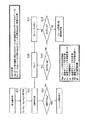
図9(A)は本発明によるフレーム同期処理を利用したネットワーク監視制御の一例を示すフローチャートであり、(B)は誤り率QBERの変化に応じた位相補正およびフレーム同期処理の一例を示す模式的グラフである。本適用例では図9(A)のシーケンスに基づいてシステムの障害検出と復旧作業を行う。 FIG. 9A is a flowchart showing an example of network monitoring control using frame synchronization processing according to the present invention, and FIG. 9B is a schematic diagram showing an example of phase correction and frame synchronization processing according to a change in error rate QBER. It is a graph. In this application example, system failure detection and recovery work are performed based on the sequence of FIG.
モニタ212は、上述したように、量子暗号鍵配布S101において算出されたQBERを監視し、制御部211はQBERとフレーム同期処理用の閾値Qbitとを比較し(ステップS102)、QBER<Qbitであれば、さらに位相補正処理用の閾値Qphaseと比較する(ステップS103)。QBER<Qphaseであれば(ステップS103のYes)、後続する鍵生成フロー、ここでは誤り訂正、残留誤り検出および秘匿増強の各処理が実行される(ステップS104)。
As described above, the
これに対して、QBER<Qbitであるが(ステップS102のYes)、位相補正処理用の閾値Qphase以上に悪化している場合には(ステップS103のNo)、位相補正処理が実行される(ステップS105)。なお、「位相ずれ」とは光子の通過/到達タイミングとクロックタイミングとのずれをいう。「位相補正処理」としては、非特許文献6に記載された位相整合(Phase alignment)を用いる方法あるいは位相制御部を制御してクロックタイミングをシフトさせながらモニタ212で最小のQBERとなるタイミングに合わせる処理などがある。
On the other hand, if QBER <Q bit (Yes in step S102), but worse than the threshold Q phase for phase correction processing (No in step S103), the phase correction processing is executed. (Step S105). The “phase shift” refers to a shift between the photon passage / arrival timing and the clock timing. As the “phase correction processing”, a method using phase alignment described in
位相補正処理S105が終了すると、続いてフレーム同期処理を実行する(ステップS106)。すでに定義したように、「フレーム同期」とは送信側と受信側との間で情報ビットの同期が取れていること、すなわちビット対応の正しい認識が成立している状態をいい、「フレーム同期ずれ」とはビット対応が誤認識されている状態をいう。また「フレーム同期処理」とは、ビット対応をシフトさせながらQBERが最小となるビット対応に再設定することであるが、具体的には後述するフレーム同期処理の項で説明する。 When the phase correction process S105 ends, the frame synchronization process is subsequently executed (step S106). As already defined, “frame synchronization” means that the information bits are synchronized between the transmitting side and the receiving side, that is, the correct recognition of the bit correspondence is established. "Means a state in which bit correspondence is erroneously recognized. “Frame synchronization processing” means resetting to bit correspondence that minimizes QBER while shifting bit correspondence, and will be specifically described in the section of frame synchronization processing described later.
フレーム同期処理S106が終了すると、制御部211は再計算されたQBERと盗聴検出用の閾値QEveとを比較する(ステップS107)。QBER<QEveであれば(ステップS107のYes)、再びステップS102に戻る。
When the frame synchronization processing S106 ends, the
他方、QBERがフレーム同期処理用の閾値Qbit以上に悪化していれば(ステップS102のNo)、上述したフレーム同期処理(ステップS106)を行い、続いてステップS107を実行する。 On the other hand, if the QBER is worse than the threshold value Q bit for frame synchronization processing (No in step S102), the above-described frame synchronization processing (step S106) is performed, and then step S107 is executed.
ここで位相補正処理S105を実行した後にフレーム同期処理S106を実行するのは、位相補正処理によってクロックの位相が変化し、フレーム同期ずれを誘発している可能性があるからである。また一般的に、フレーム同期処理と位相補正処理とを比べると、フレーム同期処理に要する時間の方が位相補正処理のそれと比べて格段に短いために、位相補正処理を行うに当たって、追加してフレーム同期処理を行うことに時間的な損失が大きくないからでもある。 The reason why the frame synchronization process S106 is executed after the phase correction process S105 is executed is that there is a possibility that the phase of the clock has changed due to the phase correction process and a frame synchronization shift has been induced. In general, when comparing frame synchronization processing and phase correction processing, the time required for frame synchronization processing is much shorter than that of phase correction processing. This is also because there is no significant time loss in performing the synchronization process.
ステップS107においてQBERがQEve以上に悪化していれば(ステップS107のNo)、制御部211はQBER<QEveとなるまで位相補正処理S105およびフレーム同期処理S106を所定回数(N)だけ連続して繰り返す(ステップS108)。所定回数繰り返してもQBERが改善しなければ(ステップS108のYes)、その時初めて暗号鍵生成フローを中断する(ステップS109)。その際、盗聴の可能性があることを示すアラームを生成することが望ましい。
If QBER is worse than Q Eve in step S107 (No in step S107),
なお、QBERは確率的に定まる値であり有限の偏差を有する。したがってQBERの閾値QbitやQphaseを設定して「この値を超えると障害」と判断するだけではなく、「複数回連続して閾値を超えると障害」といった判断も必要である。 Note that QBER is a value determined stochastically and has a finite deviation. Therefore, it is necessary not only to set the QBER threshold value Q bit and Q phase to determine “failure if this value is exceeded” but also to determine “failure if the threshold value is exceeded multiple times in succession”.
量子鍵配布中に盗聴行為によって情報が漏れている場合にもQBERは劣化するが、この劣化はシステム復旧によって改善しない。したがって、所定回数連続して位相補正処理S105およびフレーム同期処理S106を繰り返しても復旧しない場合は、「盗聴の可能性有り」として暗号鍵の生成を中断する。 Although QBER deteriorates even when information is leaked due to wiretapping during quantum key distribution, this deterioration is not improved by system recovery. Therefore, if the phase correction process S105 and the frame synchronization process S106 are repeated for a predetermined number of times and recovery is not possible, the generation of the encryption key is interrupted as “there is a possibility of eavesdropping”.
ここで、非特許文献2および3に示した漏洩情報量推定手段を用いて盗聴された可能性のある情報量を破棄することにより暗号鍵生成は行うことができるが、ある誤り率の値を超えると安全な暗号鍵生成が行えなくなる。したがって、この値を盗聴検出用の閾値QEveとして使用する。
Here, the encryption key can be generated by discarding the amount of information that may be wiretapped using the leakage information amount estimation means shown in
また、装置内に使用しているデバイス自体の故障により誤り率が増加することもあるが、本装置の最終目的は、第三者に漏洩することなく共有暗号鍵を生成することであるから、QBERに変化を及ぼさない障害は無視できる。従って、暗号鍵生成を中断するトリガは、システム復旧後でも閾値QEveを超えている場合として構わない。 In addition, the error rate may increase due to failure of the device itself used in the device, but the ultimate purpose of this device is to generate a shared encryption key without leaking to a third party. Obstacles that do not change QBER are negligible. Therefore, the trigger for interrupting the generation of the encryption key may be a case where the threshold value Q Eve is exceeded even after the system is restored.
図9(B)は、一例としてQbit=30%、Qphase=10%、QEve=10%強に設定した場合のQBERの変化と位相補正処理S105およびフレーム同期処理S106を模式的に示したものである。図示されているように、QBERが劣化しても位相補正処理S105およびフレーム同期処理S106を実行することで復旧できるかどうかをチェックし、復旧すれば、そのまま鍵生成フローを続行することができ、鍵生成効率を改善することができる。また、何回か試みても復旧できない場合に「盗聴の可能性有り」と判断して暗号鍵の生成を中断するので、鍵生成の効率性とともに安全性も担保される。 FIG. 9B schematically shows the change in QBER and the phase correction processing S105 and the frame synchronization processing S106 when Q bit = 30%, Q phase = 10%, and Q Eve = 10% are set as an example. It is a thing. As shown in the figure, even if the QBER deteriorates, it is checked whether or not it can be recovered by executing the phase correction process S105 and the frame synchronization process S106, and if it recovers, the key generation flow can be continued as it is. Key generation efficiency can be improved. In addition, if recovery is not possible after several attempts, it is determined that “there is a possibility of eavesdropping” and the generation of the encryption key is interrupted, so that the efficiency of the key generation and the safety are ensured.
3.1)変調・検出位相ずれ
図1に示すような往復型の量子暗号鍵配布システムは、PMD(Polarization Mode Dispersion)やPDL(Polarization Dependent Loss)といった伝送路における偏波方向依存の擾乱を抑制すると共に、光子パルスに載せられた位相情報を読み取るために必要な光学干渉計を効率良く組織できる、という利点を有する。
3.1) Modulation / detection phase shift The round-trip type quantum key distribution system as shown in FIG. 1 suppresses polarization direction-dependent disturbances such as PMD (Polarization Mode Dispersion) and PDL (Polarization Dependent Loss). In addition, there is an advantage that an optical interferometer necessary for reading the phase information placed on the photon pulse can be efficiently organized.
一方、往復型のシステムであるが故に、光子パルスに位相情報を載せるために用いる位相変調器を双方向で使用する必要が生じ、位相変調器を単一方向で使用する場合と比べて高い変調タイミング精度が必要になる。ここで、光子パルスが位相変調器を通過するタイミングと位相変調器を駆動するタイミングがずれると、所望量の位相変調を施すことができなくなり、干渉計の信号対雑音比(SN比)に対応する明瞭度が低下する。この低下は即ちQBERの劣化に対応する。 On the other hand, because it is a reciprocating system, it is necessary to use the phase modulator used to put the phase information on the photon pulse in both directions, resulting in higher modulation than when using the phase modulator in a single direction. Timing accuracy is required. Here, if the timing at which the photon pulse passes through the phase modulator and the timing at which the phase modulator is driven are shifted, it becomes impossible to apply the desired amount of phase modulation, which corresponds to the signal-to-noise ratio (S / N ratio) of the interferometer. The intelligibility decreases. This decrease corresponds to QBER deterioration.
上述したように、送信器10の位相変調器101によって通過光パルスに位相変調を施し、それを可変光減衰器103によって単一光子状態まで減衰させて受信器20へ送信する。受信器20では、単一光子状態の光パルスを位相変調器205によって位相変調し干渉させることで平衡型ゲートモード光子検出器APD0、APD1(非特許文献5)で光子検出を行う。一般的に、APDにゲート電圧を印加し始めた直後に光子が入射するようにタイミング調整するとAPD内部で最も雪崩増倍が起こりやすくなることが知られている。光子入射のタイミングとAPDへのゲート電圧印加タイミングとがずれると、その分、雪崩増倍が減少し、出力電流も減少してSN比が劣化する。この劣化は即ちQBERの劣化に対応する。
As described above, the phase modulation is performed on the passing light pulse by the
このようなタイミングずれ、すなわち光子入射のタイミングと位相変調器/APDの駆動タイミングとのずれは、温度変化による光伝送路の遅延変動、電気回路の遅延変動によって引き起こされるので、変化の割合は比較的小さい。従って、クロック位相をシフトさせることで、光子入射のタイミングと位相変調器/APDの駆動タイミングとを最適位置に調整することができ、劣化前のQBERに復元させることができる。 Such timing deviation, that is, deviation between the photon incidence timing and the phase modulator / APD driving timing is caused by delay variation of the optical transmission line due to temperature change and delay variation of the electric circuit. Small. Therefore, by shifting the clock phase, the photon incidence timing and the phase modulator / APD drive timing can be adjusted to the optimum position, and the QBER before deterioration can be restored.
クロック位相の調整法はいくつか提案されている。非特許文献6には、クロック信号を可変遅延した補正クロック信号と光子検出信号との位相差を検出し、その位相差に応じてクロック信号の遅延量を変化させる温度補償遅延ロックループ(DLL)を用いた方法が記載されている(非特許文献6のFig.2参照)。また、QBERをモニタしながらクロック位相を徐々にシフトさせ、QBERが最小となるクロック位相を最適位置として設定する方法も利用可能である。
Several methods for adjusting the clock phase have been proposed.
3.2)盗聴者の存在
非特許文献2および3に記載されている盗聴者Eveの情報量は、Incoherent Attack(Individual Attack)と呼ばれる盗聴法に基づいている。この盗聴法によれば、Eveは1度に1個の光子にだけ自分の持っている量子プローブをエンタングルさせる(絡ませる)ことによって光子パルスに載せられた乱数情報をある程度盗み、Alice/Bob間で基底照合のための通信が行われるまで当該量子プローブを保持する。基底公開後に適切な観測を行うことにより盗聴者は最大限の情報を得ることができる。
3.2) Presence of eavesdropper The amount of information of eavesdropper Eve described in
非特許文献2および3によれば、QBERが11〜15%以上になると、Eveの情報がBobの情報量を上回ることが導かれている。これらのQBER閾値は理論的に導かれたものであり、実世界における様々な制約を加味するとEveに漏れ得る情報量はより小さくなるが、実装置の雑音指数を理論的に定量化することはできないために一般に上記QBER閾値を盗聴検出の閾値QEveとして使用する。
According to
その他、より現実的な盗聴法として、Eveが一旦光子パルスを受光/観測してから観測結果に基づいて再度光子パルスをBobへと送り直すIntercept/Resend Attackといった盗聴法もある。しかし、この盗聴法でEveが光子ビットに残す痕跡の大きさはIncoherent Attackのそれと比べて大きいため、この盗聴が行われている場合には誤り率はより大きく劣化する。したがって、QBER閾値QEveを10%強に設定しておけば、Incoherent Attackに加えてこの盗聴も検出できる。 In addition, as a more realistic wiretapping method, there is also a wiretapping method such as Intercept / Resend Attack in which Eve once receives / observes a photon pulse and then sends the photon pulse to Bob again based on the observation result. However, since the size of the trace that Eve leaves on the photon bit in this eavesdropping method is larger than that of Incoherent Attack, the error rate is greatly deteriorated when this eavesdropping is performed. Accordingly, if the QBER threshold value Q Eve is set to a little over 10%, this wiretapping can be detected in addition to the incoherent attack.
さらに、QBERは確率的に定まる値であり有限の偏差を有する。したがってQBERの閾値を設定して「この値を超えると障害」と判断するだけではなく、「複数回連続して閾値を超えると障害」といった判断が必要となる。具体的には、一定の長さの時間、一定の大きさの空間において、ごく稀な確率で発生する事象の確率分布はポアソン(Poisson)分布に従うことが知られている。QBERが10%とすると、1000ビットの試験ビットの中に100ビット前後の誤りが含まれており、この誤り数は10ビット分の標準偏差を持つ。つまり誤り数は90〜110ビットまで無為に揺らぎ、これに従って測定されるQBERも9%〜11%まで変化する。この確率的な誤差を小さくするためには、試験ビットを増やすか試験回数を増やすことが必要となる。 Further, QBER is a value determined stochastically and has a finite deviation. Therefore, it is necessary not only to set a threshold value of QBER and determine “failure when this value is exceeded” but also to determine “failure when the threshold value is exceeded multiple times in succession”. Specifically, it is known that the probability distribution of an event that occurs with a very rare probability in a space of a certain length of time and a certain size follows a Poisson distribution. If QBER is 10%, 1000 test bits contain errors of around 100 bits, and the number of errors has a standard deviation of 10 bits. That is, the number of errors fluctuates from 90 to 110 bits, and the QBER measured according to this fluctuates from 9% to 11%. In order to reduce this stochastic error, it is necessary to increase the number of test bits or increase the number of tests.
盗聴行為によって生じたQBER劣化は、いかなる復旧作業を施しても元に戻ることはない。したがって、システム復旧後に測定したQBERが盗聴閾値QEveより上回っている場合は「盗聴可能性有り」として暗号鍵生成を中断する。 QBER degradation caused by eavesdropping does not return to any original state even if any recovery work is performed. Therefore, if the QBER measured after the system recovery exceeds the eavesdropping threshold Q Eve, the generation of the encryption key is interrupted as “possibility of eavesdropping”.
3.3)光源・受光器障害
光子パルスを生成するレーザ源および光子パルスを検出する受光器の障害によってもQBERは劣化する。レーザ光源のエネルギー変換効率が劣化すると、出力光強度が劣化し、それによって光子受信器に到達する光強度も劣化し、受信器での光子カウント数が減少する。一方、受信器でのノイズ量は入射光強度に依らず一定であるために、結果として暗号鍵のSN比が劣化する。この劣化は即ちQBERの劣化に対応する。
3.3) Failure of light source / receiver QBER is also deteriorated by a failure of a laser source that generates photon pulses and a receiver that detects photon pulses. When the energy conversion efficiency of the laser light source is deteriorated, the output light intensity is deteriorated, whereby the light intensity reaching the photon receiver is also deteriorated, and the photon count number at the receiver is reduced. On the other hand, since the amount of noise at the receiver is constant regardless of the incident light intensity, the SN ratio of the encryption key is deteriorated as a result. This deterioration corresponds to QBER deterioration.
また、光子受信器でも光電変換効率の劣化やバイアス電圧の低下など様々な劣化要因があり、これによって同一光強度を受光していても光子カウント数は劣化する。一方、この様なデバイス劣化によってノイズ量も変化するが、一般的にSN比が劣化することが大半である。つまり、光子受信器の障害によってもQBERは劣化する。 Also, the photon receiver has various deterioration factors such as a decrease in photoelectric conversion efficiency and a decrease in bias voltage, and this causes the photon count to deteriorate even when the same light intensity is received. On the other hand, although the amount of noise also changes due to such device deterioration, generally the SN ratio generally deteriorates. That is, QBER is also deteriorated by a failure of the photon receiver.
以上のようなデバイスそのものの劣化に起因するQBERの劣化は復旧機構によって回復するものではない。したがって、本障害を検出した時にはアラームを上げ暗号鍵の生成を停止する。 The deterioration of QBER due to the deterioration of the device itself as described above is not recovered by the recovery mechanism. Therefore, when this failure is detected, an alarm is raised and the generation of the encryption key is stopped.
4.適用例2
本発明は、上記実施例の往復型だけでなく、単一方向型の量子暗号鍵配布システムにも同様に適用することができる。
4). Application example 2
The present invention can be similarly applied not only to the reciprocating type of the above embodiment but also to a unidirectional quantum cryptographic key distribution system.
図10は本発明によるフレーム同期制御を適用した単一方向型量子暗号鍵配布システムの構成を示すブロック図である。ただし、本発明の動作に関係するモニタやメモリおよび制御系は図1に示すものと同様であるから同一参照番号を付している。 FIG. 10 is a block diagram showing a configuration of a unidirectional quantum encryption key distribution system to which frame synchronization control according to the present invention is applied. However, the monitor, memory and control system related to the operation of the present invention are the same as those shown in FIG.
単一方向型量子暗号鍵配布システムにおいて、送信器(Alice)40と受信器(Bob)50とは光ファイバ伝送路30によって光学的に接続され、レーザ光源401およびクロック源403は送信器40に設けられている。
In the unidirectional quantum key distribution system, the transmitter (Alice) 40 and the receiver (Bob) 50 are optically connected by the optical
レーザ光源401はクロック源403から供給される基準クロックに従って光パルス列を出射する。光パルスは光カプラ402で2分割され、一方のパルスP1は短いパスに設けられた位相変調器405によって位相変調されて光カプラ406へ到達し、他方のパルスP2は長いパス407を通って光カプラ406に到達する。したがって、位相変調された光パルスP1*Aと遅延した光パルスP2とが時間的に相前後したダブルパルスとなり、可変光減衰器408および波長合分波器409を通して伝送路30へ送出される。
The
位相制御部404はクロック源403からの基準クロックに従って位相変調器405へ位相制御信号を出力し、それに従って位相変調器405は通過する光パルスP1に位相変調を施す。位相変調の深さは、第1実施例で述べたようにメモリ109に格納された(乱数、基底)の組み合わせに依存する。また、クロック源403の基準クロックは光送信器410によりレーザ源401とは異なる波長の光信号として波長合分波器409を通して伝送路30へ送出される。なお、第1実施例と同様に、送信器40の制御部107と受信器50の制御部211とは、光送受信器108および215を通して同様の波長多重伝送によりフレーム同期や位相補正に必要なデータや制御信号等をやり取りする。
The
受信器50では、光パルスP1*Aおよび光パルスP2が波長合分波器501を通して送信器40と同様の光学系に入射する。すなわち、それぞれの光パルスは、光カプラ502により2分割され、送信器40と同様の短いパスに設けられた位相変調器503と長いパス504とを通して光カプラ507で合波する。この場合、送信器40と受信器50との間の変調の深さの差に依存して光検出器APD0あるいはAPD1の一方で光パルスが検出できるのは、送信器40の短いパス(位相変調器405)および受信器50の長いパス504を通った光パルスP1*Aと、送信器40の長いパス407および受信器50の短いパス(位相変調器503)を通った光パルスP2*Bとが同時に光カプラ507に到達し干渉する場合である。
In the
位相制御部506は、送信器40から光受信器505を通して受信した基準クロックに従って位相変調器503へ位相制御信号を出力し、それに従って位相変調器503は通過する光パルスに位相変調を施す。位相変調の深さは、既に述べたようにメモリ214に格納された基底に依存する。
The
こうして光検出器APD0およびはAPD1により検出されたデータはモニタ212を通してメモリ213に書き込まれる。モニタ212および制御部211の監視制御は、上述した実施例で説明したとおりである。
Thus, the data detected by the photodetectors APD0 and APD1 is written into the
本発明は、量子暗号鍵配布技術に代表される共通暗号鍵配布技術を用いた高秘匿通信に利用可能である。量子暗号鍵配布方法は、単一方向型・往復型を問わない。 The present invention can be used for highly confidential communication using a common encryption key distribution technique represented by a quantum encryption key distribution technique. The quantum encryption key distribution method may be a unidirectional type or a round-trip type.
10 送信器(Alice)
20 受信器(Bob)
30 光ファイバ伝送路
101 位相変調器
102 偏光ビームスプリッタ
103 可変光減衰器
104 位相制御部
105 光受信器
106 光送信器
107 制御部
108 光送受信器
109 メモリ
110 波長合分波器
201 クロック源
202 レーザ源
203 光サーキュレータ
204 光カプラ
205 位相変調器
206 偏光ビームスプリッタ
207 波長合分波器
208 光送信器
209 光受信器
210 位相制御部
211 制御部
212 モニタ
213 メモリ
214 メモリ
215 光送受信器
10 Transmitter (Alice)
20 Receiver (Bob)
30 optical
Claims (13)
a)前記第1通信器は、それぞれビットタイミングが相対的に定められた複数のビット列からなる第1データを一の通信チャネルを通して前記第2通信器へ送信し、前記第2通信器は前記一の通信チャネルを通して前記第1通信器から受信した第2データを保存し、
b)前記第1通信器と前記第2通信器との間のビットタイミング差である第1同期ずれと、前記第2通信器内のビットタイミング差である第2同期ずれと、を仮設定し、
c)仮設定された前記第1同期ずれおよび前記第2同期ずれを所定調整範囲内で順次変更しながら、前記第2データの一部とそれに対応する前記第1データとを照合し、
d)前記照合結果に基づいて前記第1同期ずれおよび前記第2同期ずれを確定する、
ことを特徴とする同期制御方法。 In a synchronization control method for establishing bit correspondence of data to be shared between a first communication device and a second communication device connected by a plurality of communication channels,
a) The first communication device transmits first data composed of a plurality of bit strings, each of which has a relatively determined bit timing, to the second communication device through one communication channel, and the second communication device transmits the first communication device to the first communication device. Storing the second data received from the first communication device through the communication channel of
b) Temporarily setting a first synchronization shift that is a bit timing difference between the first communication device and the second communication device and a second synchronization shift that is a bit timing difference in the second communication device. ,
c) collating a part of the second data with the corresponding first data while sequentially changing the temporarily set first synchronization deviation and the second synchronization deviation within a predetermined adjustment range;
d) determining the first synchronization deviation and the second synchronization deviation based on the collation result;
A synchronization control method characterized by the above.
c.1)仮設定された前記第1同期ずれおよび仮設定された前記第2同期ずれを用いて、前記第2データの一部のビットタイミングにそれぞれ対応する前記第1データのビットタイミングを決定し、
c.2)前記第2データの前記一部の値とそれらに対応する前記第1データの値とを照合し、
c.3)仮設定された前記第1同期ずれおよび仮設定された前記第2同期ずれの少なくとも一方を所定ステップ変化させ、
c.4)前記c.1)〜c.3)を前記所定調整範囲内で繰り返す、
ことを特徴とする請求項1に記載の同期制御方法。 C)
c. 1) Using the temporarily set first synchronization shift and the temporarily set second synchronization shift, determine bit timings of the first data respectively corresponding to partial bit timings of the second data;
c. 2) collating the partial value of the second data with the value of the first data corresponding to the partial value;
c. 3) Change at least one of the temporarily set first synchronization error and the temporarily set second synchronization error by a predetermined step,
c. 4) c. 1) to c. 3) is repeated within the predetermined adjustment range,
The synchronous control method according to claim 1, wherein:
c.1)仮設定された前記第1同期ずれおよび仮設定された前記第2同期ずれを用いて、前記第2データの一部のビットタイミングにそれぞれ対応する前記第1データのビットタイミングを決定し、
c.2)前記第2データの前記一部の値とそれらに対応する前記第1データの値とを照合し、
c.3)前記照合結果が所定の閾値より良好でない場合には、仮設定された前記第1同期ずれおよび仮設定された前記第2同期ずれの少なくとも一方を所定ステップ変化させ、
c.4)前記c.1)〜c.3)を前記所定調整範囲内で繰り返し、
前記d)は、
前記c.2)で得られた前記照合結果が前記所定の閾値より良好である場合には、当該照合結果をもたらす仮設定された第1同期ずれおよび第2同期ずれを同期確立された前記第1同期ずれおよび前記第2同期ずれとして決定する、
ことを特徴とする請求項1に記載の同期制御方法。 C)
c. 1) Using the temporarily set first synchronization shift and the temporarily set second synchronization shift, determine bit timings of the first data respectively corresponding to partial bit timings of the second data;
c. 2) collating the partial value of the second data with the value of the first data corresponding to the partial value;
c. 3) If the collation result is not better than a predetermined threshold, change at least one of the temporarily set first synchronization shift and the temporarily set second synchronization shift by a predetermined step,
c. 4) c. 1) to c. 3) is repeated within the predetermined adjustment range,
Said d)
C. If the collation result obtained in 2) is better than the predetermined threshold value, the first synchronization deviation and the first synchronization deviation, which are temporarily set to produce the collation result, are synchronized with each other. And determining as the second synchronization shift,
The synchronous control method according to claim 1, wherein:
e.1)仮設定された前記第1同期ずれおよび仮設定された前記第2同期ずれを用いて、前記第2データの一部のビットタイミングにそれぞれ対応する前記第1データのビットタイミングを決定し、
e.2)前記第2データの前記一部の値とそれらに対応する前記第1データの値とを照合し、
e.3)前記照合結果が第1閾値より良好でない場合には、仮設定された前記第1同期ずれを所定ステップ変化させ、
e.4)前記e.1)〜e.3)を前記第1同期ずれの所定調整範囲内で繰り返し、
e.5)前記e.2)で得られた前記照合結果が前記第1閾値より良好である場合には、当該照合結果をもたらす仮設定された第1同期ずれを同期確立された前記第1同期ずれとして決定し、
e.6)前記e.2)で得られた前記照合結果が前記第1閾値より良好で、かつ、第2閾値より良好でない場合には、仮設定された前記第2同期ずれを所定ステップ変化させ、
e.7)前記第2データの前記一部の値とそれらに対応する前記第1データの値とを照合し、
e.8)前記e.7)で得られた前記照合結果が前記第2閾値より良好でない場合には、前記e.6)〜e.7)を前記第2同期ずれの所定調整範囲内で繰り返し、
e.9)前記e.7)で得られた前記照合結果が前記第2閾値より良好である場合には、当該照合結果をもたらす仮設定された第2同期ずれを同期確立された前記第2同期ずれとして決定する、
ことを特徴とする請求項1に記載の同期制御方法。 C) and d)
e. 1) Using the temporarily set first synchronization shift and the temporarily set second synchronization shift, determine bit timings of the first data respectively corresponding to partial bit timings of the second data;
e. 2) collating the partial value of the second data with the value of the first data corresponding to the partial value;
e. 3) If the collation result is not better than the first threshold, the temporarily set first synchronization shift is changed by a predetermined step,
e. 4) e. 1) to e. 3) is repeated within a predetermined adjustment range of the first synchronization shift,
e. 5) said e. If the collation result obtained in 2) is better than the first threshold value, the provisionally set first synchronization deviation that results in the collation result is determined as the first synchronization deviation that has been established,
e. 6) said e. When the collation result obtained in 2) is better than the first threshold and not better than the second threshold, the temporarily set second synchronization shift is changed by a predetermined step,
e. 7) collating the partial value of the second data with the value of the first data corresponding to the partial value;
e. 8) said e. When the collation result obtained in 7) is not better than the second threshold value, the e. 6) to e. 7) is repeated within a predetermined adjustment range of the second synchronization shift,
e. 9) e. When the collation result obtained in 7) is better than the second threshold value, the provisionally set second synchronization deviation that causes the collation result is determined as the second synchronization deviation that is established in synchronization.
The synchronous control method according to claim 1, wherein:
前記第1通信器は、
それぞれビットタイミングが相対的に定められた複数のビット列からなる第1データを一の通信チャネルを通して前記第2通信器へ送信し、
前記第1通信器と前記第2通信器との間のビットタイミング差である第1同期ずれを仮設定し、
前記第2通信器は、
前記一の通信チャネルを通して前記第1通信器から受信した第2データを保存し、
前記第2通信器内のビットタイミング差である第2同期ずれを仮設定し、
仮設定された第2同期ずれが所定調整範囲で変化した場合の前記第2データの一部を前記第1通信器へ送信し、
前記第1通信器は、
仮設定された第1同期ずれを所定調整範囲内で変化させながら、前記第2通信器から受信した前記第2データの一部とそれに対応する前記第1データとを照合し、
前記照合結果に基づいて前記第1同期ずれおよび前記第2同期ずれを確定する、
ことを特徴とする同期制御方法。 In a synchronization control method for establishing bit correspondence of data to be shared between a first communication device and a second communication device connected by a plurality of communication channels,
The first communicator is
Transmitting first data consisting of a plurality of bit strings, each of which is relatively determined in bit timing, to the second communication device through one communication channel;
Temporarily setting a first synchronization shift which is a bit timing difference between the first communication device and the second communication device;
The second communicator is
Storing second data received from the first communicator through the one communication channel;
Temporarily set a second synchronization shift which is a bit timing difference in the second communication device,
A part of the second data when the temporarily set second synchronization shift changes within a predetermined adjustment range is transmitted to the first communication device;
The first communicator is
While changing the temporarily set first synchronization deviation within a predetermined adjustment range, collate a part of the second data received from the second communication device with the corresponding first data,
Determining the first synchronization shift and the second synchronization shift based on the verification result;
A synchronization control method characterized by the above.
前記第2通信器は、
それぞれビットタイミングが相対的に定められた複数のビット列からなる第1データを一の通信チャネルを通して前記第1通信器から受信する受信手段と、
受信したデータを第2データを格納する格納手段と、
前記第2通信器内のビットタイミング差である第2同期ずれを仮設定し、仮設定された第2同期ずれが所定調整範囲で変化した場合の前記第2データの一部を生成する生成手段と、
前記第2データの一部を前記第1通信器へ送信する送信手段と、
を有し、
前記第1通信器は、前記第1通信器と前記第2通信器との間のビットタイミング差である第1同期ずれを仮設定し、仮設定された第1同期ずれを所定調整範囲内で変化させながら、前記第2通信器から受信した前記第2データの一部とそれに対応する前記第1データとを照合し、前記照合結果に基づいて前記第1同期ずれおよび前記第2同期ずれを確定する制御手段を有する、
ことを特徴とする同期制御システム。 In a synchronous control system for establishing bit correspondence of data to be shared between a first communication device and a second communication device connected by a plurality of communication channels,
The second communicator is
Receiving means for receiving, from the first communication device, first data consisting of a plurality of bit strings, each of which has a relatively determined bit timing, through one communication channel;
Storage means for storing received data as second data;
Generation means for temporarily setting a second synchronization shift that is a bit timing difference in the second communication device, and generating a part of the second data when the temporarily set second synchronization shift changes within a predetermined adjustment range When,
Transmitting means for transmitting a part of the second data to the first communication device;
Have
The first communication device temporarily sets a first synchronization shift that is a bit timing difference between the first communication device and the second communication device, and the temporarily set first synchronization shift is within a predetermined adjustment range. While changing, a part of the second data received from the second communication device and the first data corresponding thereto are collated, and the first synchronization deviation and the second synchronization deviation are determined based on the collation result. Having control means to confirm,
A synchronous control system characterized by that.
前記送信器は、
それぞれビットタイミングが相対的に定められた複数のビット列からなる第1データおよび第2データを格納する第1格納手段と、
前記第1および第2データに従って光信号を変調する第1変調手段と、
変調された光信号を一の通信チャネルを通して前記受信器へ送信する第1通信手段と、
前記受信器との間で他の通信チャネルを通してデータ通信を行うための第1送受信手段と、
を有し、
前記受信器は、
第3データを格納する第2格納手段と、
前記一の通信チャネルを通して前記送信器から光信号を受信する第2通信手段と、
前記受信した光信号を前記第3データに従って変調する第2変調手段と、
前記受信した光信号と前記第2変調手段により変調された光信号とに基づいて第4データを検出する光検出手段と、
前記第4データを格納する第3格納手段と、
前記送信器との間で前記他の通信チャネルを通してデータ通信を行うための第2送受信手段と、
前記第2変調手段と前記光検出手段との間のビットタイミング差である第2同期ずれを仮設定し、仮設定された第2同期ずれが所定調整範囲で変化した場合の前記第3データおよび第4データの一部を前記送信器へ送信する受信側制御手段と、
を有し、
前記送信器は、さらに、
前記第1変調手段と前記光検出手段との間のビットタイミング差である第1同期ずれを仮設定し、仮設定された第1同期ずれを所定調整範囲内で変化させながら、前記受信器から受信した前記第3データおよび前記第4データの一部と、それに対応する前記第1データおよび前記第2データと、を照合し、前記照合結果に基づいて前記第1同期ずれおよび前記第2同期ずれを確定する送信側制御手段を有する、
ことを特徴とする通信システム。 In a communication system in which a transmitter and a receiver are connected via an optical transmission line and communicate via a plurality of communication channels.
The transmitter is
First storage means for storing first data and second data each consisting of a plurality of bit strings each having a relatively determined bit timing;
First modulation means for modulating an optical signal in accordance with the first and second data;
First communication means for transmitting the modulated optical signal to the receiver through a communication channel;
First transmitting / receiving means for performing data communication with the receiver through another communication channel;
Have
The receiver is
Second storage means for storing third data;
Second communication means for receiving an optical signal from the transmitter through the one communication channel;
Second modulation means for modulating the received optical signal according to the third data;
Light detecting means for detecting fourth data based on the received optical signal and the optical signal modulated by the second modulating means;
Third storage means for storing the fourth data;
Second transmitting / receiving means for performing data communication with the transmitter through the other communication channel;
Temporarily setting a second synchronization shift that is a bit timing difference between the second modulation means and the light detection means, and the third data when the temporarily set second synchronization shift changes within a predetermined adjustment range, and Receiving-side control means for transmitting a part of the fourth data to the transmitter;
Have
The transmitter further includes:
Temporarily setting a first synchronization shift that is a bit timing difference between the first modulation means and the light detection means, and changing the temporarily set first synchronization shift within a predetermined adjustment range, The received third data and a part of the fourth data are compared with the corresponding first data and second data, and the first synchronization shift and the second synchronization are performed based on the comparison result. Having transmission-side control means for determining the deviation,
A communication system characterized by the above.
それぞれビットタイミングが相対的に定められた複数のビット列からなる第1データを一の通信チャネルを通して第1通信器から第2通信器へ送信することで前記第2通信器が受信したデータを第2データとして保存するステップと、
前記第1通信器と前記第2通信器との間のビットタイミング差である第1同期ずれと、前記第2通信器内のビットタイミング差である第2同期ずれと、を仮設定するステップと、
仮設定された前記第1同期ずれおよび前記第2同期ずれを所定調整範囲内で順次変更しながら、前記第2データの一部とそれに対応する前記第1データとを照合するステップと、
前記照合結果に基づいて前記第1同期ずれおよび前記第2同期ずれを確定するステップと、
を有することを特徴とする同期制御プログラム。
In a program for causing a computer to execute synchronous control for establishing bit correspondence of data to be shared between a first communication device and a second communication device connected by a plurality of communication channels,
By transmitting first data consisting of a plurality of bit strings, each of which has a relatively determined bit timing, from the first communication device to the second communication device through one communication channel, the data received by the second communication device is second Saving as data,
Temporarily setting a first synchronization shift that is a bit timing difference between the first communication device and the second communication device and a second synchronization shift that is a bit timing difference in the second communication device; ,
Collating a part of the second data with the corresponding first data while sequentially changing the temporarily set first synchronization deviation and the second synchronization deviation within a predetermined adjustment range;
Determining the first synchronization error and the second synchronization error based on the verification result;
A synchronization control program comprising:
Priority Applications (3)
| Application Number | Priority Date | Filing Date | Title |
|---|---|---|---|
| JP2005200974A JP4662040B2 (en) | 2005-07-08 | 2005-07-08 | Communication system and synchronization control method thereof |
| EP06014154.6A EP1742408B1 (en) | 2005-07-08 | 2006-07-07 | Communication system and synchronization control method |
| US11/482,016 US8391491B2 (en) | 2005-07-08 | 2006-07-07 | Communication system and synchronization control method |
Applications Claiming Priority (1)
| Application Number | Priority Date | Filing Date | Title |
|---|---|---|---|
| JP2005200974A JP4662040B2 (en) | 2005-07-08 | 2005-07-08 | Communication system and synchronization control method thereof |
Publications (2)
| Publication Number | Publication Date |
|---|---|
| JP2007020013A JP2007020013A (en) | 2007-01-25 |
| JP4662040B2 true JP4662040B2 (en) | 2011-03-30 |
Family
ID=37202550
Family Applications (1)
| Application Number | Title | Priority Date | Filing Date |
|---|---|---|---|
| JP2005200974A Active JP4662040B2 (en) | 2005-07-08 | 2005-07-08 | Communication system and synchronization control method thereof |
Country Status (3)
| Country | Link |
|---|---|
| US (1) | US8391491B2 (en) |
| EP (1) | EP1742408B1 (en) |
| JP (1) | JP4662040B2 (en) |
Families Citing this family (24)
| Publication number | Priority date | Publication date | Assignee | Title |
|---|---|---|---|---|
| JP4654649B2 (en) * | 2004-10-07 | 2011-03-23 | ソニー株式会社 | Quantum cryptography communication method, quantum cryptography communication apparatus, and quantum cryptography communication system |
| US7436961B2 (en) * | 2005-03-08 | 2008-10-14 | Magiq Technologies, Inc. | Sentinel synchronization method for enhancing QKD security |
| JP2007274300A (en) * | 2006-03-31 | 2007-10-18 | Hitachi Information & Communication Engineering Ltd | Synchronization processing method in common key cipher communication |
| US7539314B2 (en) * | 2006-08-14 | 2009-05-26 | Magiq Technologies, Inc. | Frame synchronization method for QKD systems |
| JP5424008B2 (en) * | 2006-12-19 | 2014-02-26 | 日本電気株式会社 | Shared information management method and system |
| JP5347644B2 (en) * | 2009-03-27 | 2013-11-20 | 日本電気株式会社 | Optical communication system and method, transmitter and receiver, quantum cryptography key distribution system and method |
| JP5282147B2 (en) * | 2010-02-15 | 2013-09-04 | 株式会社日立製作所 | Cryptographic communication system and transmitter and receiver used therefor |
| US8781129B2 (en) * | 2011-02-23 | 2014-07-15 | General Electric Company | Systems, methods, and apparatus for electrical grid quantum key distribution |
| US9866379B2 (en) | 2011-09-30 | 2018-01-09 | Los Alamos National Security, Llc | Polarization tracking system for free-space optical communication, including quantum communication |
| KR20150031245A (en) * | 2012-05-23 | 2015-03-23 | 유니버시티 오브 리드스 | Secure communication |
| US8693691B2 (en) | 2012-05-25 | 2014-04-08 | The Johns Hopkins University | Embedded authentication protocol for quantum key distribution systems |
| US9819418B2 (en) | 2012-08-17 | 2017-11-14 | Los Alamos National Security, Llc | Quantum communications system with integrated photonic devices |
| KR101559076B1 (en) * | 2014-01-24 | 2015-10-08 | 고려대학교 산학협력단 | Efficient information reconciliation method using turbo codes over the quantum channel |
| CN105827397B (en) | 2015-01-08 | 2019-10-18 | 阿里巴巴集团控股有限公司 | Quantum key distribution system, method and device based on credible relaying |
| CN106470104B (en) * | 2015-08-20 | 2020-02-07 | 阿里巴巴集团控股有限公司 | Method, device, terminal equipment and system for generating shared key |
| US10142033B2 (en) * | 2015-11-27 | 2018-11-27 | Korea Institute Of Science And Technology | Communication apparatus and communication method for successive quantum key distribution |
| CN107135066B (en) * | 2016-02-29 | 2020-08-07 | 华为技术有限公司 | Original key recovery device and method |
| SG10201901665XA (en) | 2016-03-22 | 2019-03-28 | Lyteloop Technologies Llc | Data in motion storage system and method |
| CN106656491B (en) * | 2016-12-30 | 2019-08-09 | 北京信息科学技术研究院 | The compensation method of half-wave voltage of phase modulator in a kind of quantum key dispatching system |
| US11115199B2 (en) | 2018-07-18 | 2021-09-07 | Kabushiki Kaisha Toshiba | Information processing method, and computer program product |
| SG11202007731QA (en) | 2018-08-10 | 2020-09-29 | Lyteloop Technologies Llc | System and method for extending path length of a wave signal using angle multiplexing |
| AU2019377800A1 (en) * | 2018-11-05 | 2021-03-18 | Nkb Properties Management, Llc | Systems and methods for building, operating and controlling multiple amplifiers, regenerators and transceivers using shared common components |
| US12010223B2 (en) * | 2020-07-13 | 2024-06-11 | Arizona Board Of Regents On Behalf Of The University Of Arizona | Joint twin-field quantum key distribution cryptosystem |
| JPWO2022163575A1 (en) * | 2021-01-29 | 2022-08-04 |
Citations (5)
| Publication number | Priority date | Publication date | Assignee | Title |
|---|---|---|---|---|
| JPH08256086A (en) * | 1995-03-17 | 1996-10-01 | Sony Corp | Spread spectrum communication system |
| JPH09200197A (en) * | 1996-01-12 | 1997-07-31 | Nec Corp | Synchronization stream ciphering device and decoder applied to the device |
| JP2000174747A (en) * | 1998-12-07 | 2000-06-23 | Nippon Telegr & Teleph Corp <Ntt> | Quantum cryptography device |
| JP2004112278A (en) * | 2002-09-18 | 2004-04-08 | Mitsubishi Electric Corp | Quantum key delivery method and communication equipment |
| WO2005018185A1 (en) * | 2003-08-13 | 2005-02-24 | Philips Intellectual Property & Standards Gmbh | Encryption method and decoding method for a digital transmission system |
Family Cites Families (19)
| Publication number | Priority date | Publication date | Assignee | Title |
|---|---|---|---|---|
| JPS61169047A (en) * | 1985-01-22 | 1986-07-30 | Kokusai Denshin Denwa Co Ltd <Kdd> | Detection system of propagation delay time variance in optical fiber transmission line |
| AU674198B2 (en) * | 1992-12-24 | 1996-12-12 | British Telecommunications Public Limited Company | System and method for key distribution using quantum cryptography |
| CA2169553C (en) * | 1993-09-09 | 1999-12-07 | Paul David Townsend | System and method for key distribution using quantum cryptography |
| EP0717895B1 (en) * | 1993-09-09 | 1998-11-25 | BRITISH TELECOMMUNICATIONS public limited company | Key distribution in a multiple access network using quantum cryptography |
| CA2168851C (en) * | 1993-09-09 | 1999-11-02 | Keith James Blow | System and method for quantum cryptography |
| US6177922B1 (en) * | 1997-04-15 | 2001-01-23 | Genesis Microship, Inc. | Multi-scan video timing generator for format conversion |
| US6137734A (en) * | 1999-03-30 | 2000-10-24 | Lsi Logic Corporation | Computer memory interface having a memory controller that automatically adjusts the timing of memory interface signals |
| US6662223B1 (en) * | 1999-07-01 | 2003-12-09 | Cisco Technology, Inc. | Protocol to coordinate network end points to measure network latency |
| US6961930B1 (en) * | 1999-09-22 | 2005-11-01 | Hewlett-Packard Development Company, L.P. | Efficient, transparent and flexible latency sampling |
| US7006635B2 (en) * | 2000-08-31 | 2006-02-28 | The United States Of America As Represented By The Secretary Of The Navy | Method and apparatus for clock synchronization using quantum mechanical non-locality effects |
| US6956868B2 (en) * | 2001-02-15 | 2005-10-18 | Chunming Qiao | Labeled optical burst switching for IP-over-WDM integration |
| JP2002344898A (en) * | 2001-05-17 | 2002-11-29 | Pioneer Electronic Corp | Video display device, audio adjusting device, video and audio output device, and method for synchronizing video and audio |
| IL144369A (en) * | 2001-07-17 | 2009-06-15 | Eli Yanovsky | Secure communication system and method using shared random source for key changing |
| JP2004032679A (en) * | 2002-02-28 | 2004-01-29 | Matsushita Electric Ind Co Ltd | Communication apparatus and communication system |
| US7627126B1 (en) * | 2002-10-15 | 2009-12-01 | Bbn Technologies Corp. | Systems and methods for implementing path length control for quantum cryptographic systems |
| JP4632652B2 (en) * | 2003-10-10 | 2011-02-16 | 日本電気株式会社 | Quantum cryptographic key distribution system and synchronization method used therefor |
| US20050135167A1 (en) * | 2003-10-16 | 2005-06-23 | Nec Plasma Display Corporation | Memory access circuit for adjusting delay of internal clock signal used for memory control |
| US7437764B1 (en) * | 2003-11-14 | 2008-10-14 | Symantec Corporation | Vulnerability assessment of disk images |
| JP4753895B2 (en) * | 2007-02-20 | 2011-08-24 | ルネサスエレクトロニクス株式会社 | Array type processor having delay adjustment circuit |
-
2005
- 2005-07-08 JP JP2005200974A patent/JP4662040B2/en active Active
-
2006
- 2006-07-07 US US11/482,016 patent/US8391491B2/en active Active
- 2006-07-07 EP EP06014154.6A patent/EP1742408B1/en active Active
Patent Citations (5)
| Publication number | Priority date | Publication date | Assignee | Title |
|---|---|---|---|---|
| JPH08256086A (en) * | 1995-03-17 | 1996-10-01 | Sony Corp | Spread spectrum communication system |
| JPH09200197A (en) * | 1996-01-12 | 1997-07-31 | Nec Corp | Synchronization stream ciphering device and decoder applied to the device |
| JP2000174747A (en) * | 1998-12-07 | 2000-06-23 | Nippon Telegr & Teleph Corp <Ntt> | Quantum cryptography device |
| JP2004112278A (en) * | 2002-09-18 | 2004-04-08 | Mitsubishi Electric Corp | Quantum key delivery method and communication equipment |
| WO2005018185A1 (en) * | 2003-08-13 | 2005-02-24 | Philips Intellectual Property & Standards Gmbh | Encryption method and decoding method for a digital transmission system |
Also Published As
| Publication number | Publication date |
|---|---|
| EP1742408A2 (en) | 2007-01-10 |
| EP1742408B1 (en) | 2018-03-07 |
| US20070058810A1 (en) | 2007-03-15 |
| US8391491B2 (en) | 2013-03-05 |
| JP2007020013A (en) | 2007-01-25 |
| EP1742408A3 (en) | 2008-07-23 |
Similar Documents
| Publication | Publication Date | Title |
|---|---|---|
| JP4662040B2 (en) | Communication system and synchronization control method thereof | |
| JP4888630B2 (en) | Communication system and supervisory control method thereof | |
| US7616765B2 (en) | Method and system for generating shared information | |
| US8949300B2 (en) | Circuit and method for controlling quality of random numbers | |
| JP4173422B2 (en) | Quantum key distribution method and quantum key distribution system | |
| JP5424008B2 (en) | Shared information management method and system | |
| US6748083B2 (en) | Method and apparatus for free-space quantum key distribution in daylight | |
| US9160529B2 (en) | Secret communication system and method for generating shared secret information | |
| US7181011B2 (en) | Key bank systems and methods for QKD | |
| CN108604425B (en) | Random number sequence generation device, quantum cipher transmitter, and quantum cipher communication system | |
| US20070133798A1 (en) | Quantum cryptography on a multi-drop optical network | |
| JP2002064480A (en) | Method and device for distributing encryption key | |
| EP4107902A1 (en) | A method for quantum key distribution, a method for transmitting an optical signal, a method for receiving an optical signal, and a receiver of an optical signal for quantum key distribution | |
| US20070255679A1 (en) | Method and system for encrypted communications using multi-valued modulation | |
| WO2014068959A1 (en) | Light-receiving device in optical communication system, photon-detector control method and device, and photon-detector dark-count-rate evaluation method | |
| JP2009218744A (en) | Method and system of frame synchronization for feeble optical communication | |
| JP6257042B2 (en) | Quantum key distribution system and quantum key distribution method | |
| Hughes et al. | Free-space quantum cryptography in daylight | |
| JP4417360B2 (en) | Quantum communication system | |
| Chan et al. | Quantum key distribution | |
| Futami et al. | Physical layer encryption by Y-00 protocol for secure optical interconnection between data centers |
Legal Events
| Date | Code | Title | Description |
|---|---|---|---|
| A621 | Written request for application examination |
Free format text: JAPANESE INTERMEDIATE CODE: A621 Effective date: 20080611 |
|
| A977 | Report on retrieval |
Free format text: JAPANESE INTERMEDIATE CODE: A971007 Effective date: 20101129 |
|
| TRDD | Decision of grant or rejection written | ||
| A01 | Written decision to grant a patent or to grant a registration (utility model) |
Free format text: JAPANESE INTERMEDIATE CODE: A01 Effective date: 20101208 |
|
| A01 | Written decision to grant a patent or to grant a registration (utility model) |
Free format text: JAPANESE INTERMEDIATE CODE: A01 |
|
| A61 | First payment of annual fees (during grant procedure) |
Free format text: JAPANESE INTERMEDIATE CODE: A61 Effective date: 20101221 |
|
| R150 | Certificate of patent or registration of utility model |
Ref document number: 4662040 Country of ref document: JP Free format text: JAPANESE INTERMEDIATE CODE: R150 Free format text: JAPANESE INTERMEDIATE CODE: R150 |
|
| FPAY | Renewal fee payment (event date is renewal date of database) |
Free format text: PAYMENT UNTIL: 20140114 Year of fee payment: 3 |