JP4658304B2 - Method for manufacturing magnetoresistive effect structure and method for manufacturing magnetoresistive head - Google Patents
Method for manufacturing magnetoresistive effect structure and method for manufacturing magnetoresistive head Download PDFInfo
- Publication number
- JP4658304B2 JP4658304B2 JP2000312489A JP2000312489A JP4658304B2 JP 4658304 B2 JP4658304 B2 JP 4658304B2 JP 2000312489 A JP2000312489 A JP 2000312489A JP 2000312489 A JP2000312489 A JP 2000312489A JP 4658304 B2 JP4658304 B2 JP 4658304B2
- Authority
- JP
- Japan
- Prior art keywords
- magnetic field
- femn
- antiferromagnetic
- layer
- nife
- Prior art date
- Legal status (The legal status is an assumption and is not a legal conclusion. Google has not performed a legal analysis and makes no representation as to the accuracy of the status listed.)
- Expired - Fee Related
Links
Images


Classifications
-
- G—PHYSICS
- G11—INFORMATION STORAGE
- G11B—INFORMATION STORAGE BASED ON RELATIVE MOVEMENT BETWEEN RECORD CARRIER AND TRANSDUCER
- G11B5/00—Recording by magnetisation or demagnetisation of a record carrier; Reproducing by magnetic means; Record carriers therefor
- G11B5/127—Structure or manufacture of heads, e.g. inductive
- G11B5/33—Structure or manufacture of flux-sensitive heads, i.e. for reproduction only; Combination of such heads with means for recording or erasing only
- G11B5/39—Structure or manufacture of flux-sensitive heads, i.e. for reproduction only; Combination of such heads with means for recording or erasing only using magneto-resistive devices or effects
- G11B5/3903—Structure or manufacture of flux-sensitive heads, i.e. for reproduction only; Combination of such heads with means for recording or erasing only using magneto-resistive devices or effects using magnetic thin film layers or their effects, the films being part of integrated structures
-
- B—PERFORMING OPERATIONS; TRANSPORTING
- B82—NANOTECHNOLOGY
- B82Y—SPECIFIC USES OR APPLICATIONS OF NANOSTRUCTURES; MEASUREMENT OR ANALYSIS OF NANOSTRUCTURES; MANUFACTURE OR TREATMENT OF NANOSTRUCTURES
- B82Y25/00—Nanomagnetism, e.g. magnetoimpedance, anisotropic magnetoresistance, giant magnetoresistance or tunneling magnetoresistance
-
- B—PERFORMING OPERATIONS; TRANSPORTING
- B82—NANOTECHNOLOGY
- B82Y—SPECIFIC USES OR APPLICATIONS OF NANOSTRUCTURES; MEASUREMENT OR ANALYSIS OF NANOSTRUCTURES; MANUFACTURE OR TREATMENT OF NANOSTRUCTURES
- B82Y10/00—Nanotechnology for information processing, storage or transmission, e.g. quantum computing or single electron logic
-
- B—PERFORMING OPERATIONS; TRANSPORTING
- B82—NANOTECHNOLOGY
- B82Y—SPECIFIC USES OR APPLICATIONS OF NANOSTRUCTURES; MEASUREMENT OR ANALYSIS OF NANOSTRUCTURES; MANUFACTURE OR TREATMENT OF NANOSTRUCTURES
- B82Y40/00—Manufacture or treatment of nanostructures
-
- H—ELECTRICITY
- H01—ELECTRIC ELEMENTS
- H01F—MAGNETS; INDUCTANCES; TRANSFORMERS; SELECTION OF MATERIALS FOR THEIR MAGNETIC PROPERTIES
- H01F10/00—Thin magnetic films, e.g. of one-domain structure
- H01F10/32—Spin-exchange-coupled multilayers, e.g. nanostructured superlattices
- H01F10/324—Exchange coupling of magnetic film pairs via a very thin non-magnetic spacer, e.g. by exchange with conduction electrons of the spacer
- H01F10/3268—Exchange coupling of magnetic film pairs via a very thin non-magnetic spacer, e.g. by exchange with conduction electrons of the spacer the exchange coupling being asymmetric, e.g. by use of additional pinning, by using antiferromagnetic or ferromagnetic coupling interface, i.e. so-called spin-valve [SV] structure, e.g. NiFe/Cu/NiFe/FeMn
-
- H—ELECTRICITY
- H01—ELECTRIC ELEMENTS
- H01F—MAGNETS; INDUCTANCES; TRANSFORMERS; SELECTION OF MATERIALS FOR THEIR MAGNETIC PROPERTIES
- H01F10/00—Thin magnetic films, e.g. of one-domain structure
- H01F10/32—Spin-exchange-coupled multilayers, e.g. nanostructured superlattices
- H01F10/324—Exchange coupling of magnetic film pairs via a very thin non-magnetic spacer, e.g. by exchange with conduction electrons of the spacer
- H01F10/3295—Spin-exchange coupled multilayers wherein the magnetic pinned or free layers are laminated without anti-parallel coupling within the pinned and free layers
-
- H—ELECTRICITY
- H01—ELECTRIC ELEMENTS
- H01F—MAGNETS; INDUCTANCES; TRANSFORMERS; SELECTION OF MATERIALS FOR THEIR MAGNETIC PROPERTIES
- H01F41/00—Apparatus or processes specially adapted for manufacturing or assembling magnets, inductances or transformers; Apparatus or processes specially adapted for manufacturing materials characterised by their magnetic properties
- H01F41/14—Apparatus or processes specially adapted for manufacturing or assembling magnets, inductances or transformers; Apparatus or processes specially adapted for manufacturing materials characterised by their magnetic properties for applying magnetic films to substrates
- H01F41/30—Apparatus or processes specially adapted for manufacturing or assembling magnets, inductances or transformers; Apparatus or processes specially adapted for manufacturing materials characterised by their magnetic properties for applying magnetic films to substrates for applying nanostructures, e.g. by molecular beam epitaxy [MBE]
- H01F41/302—Apparatus or processes specially adapted for manufacturing or assembling magnets, inductances or transformers; Apparatus or processes specially adapted for manufacturing materials characterised by their magnetic properties for applying magnetic films to substrates for applying nanostructures, e.g. by molecular beam epitaxy [MBE] for applying spin-exchange-coupled multilayers, e.g. nanostructured superlattices
- H01F41/303—Apparatus or processes specially adapted for manufacturing or assembling magnets, inductances or transformers; Apparatus or processes specially adapted for manufacturing materials characterised by their magnetic properties for applying magnetic films to substrates for applying nanostructures, e.g. by molecular beam epitaxy [MBE] for applying spin-exchange-coupled multilayers, e.g. nanostructured superlattices with exchange coupling adjustment of magnetic film pairs, e.g. interface modifications by reduction, oxidation
- H01F41/304—Apparatus or processes specially adapted for manufacturing or assembling magnets, inductances or transformers; Apparatus or processes specially adapted for manufacturing materials characterised by their magnetic properties for applying magnetic films to substrates for applying nanostructures, e.g. by molecular beam epitaxy [MBE] for applying spin-exchange-coupled multilayers, e.g. nanostructured superlattices with exchange coupling adjustment of magnetic film pairs, e.g. interface modifications by reduction, oxidation using temporary decoupling, e.g. involving blocking, Néel or Curie temperature transitions by heat treatment in presence/absence of a magnetic field
-
- G—PHYSICS
- G11—INFORMATION STORAGE
- G11B—INFORMATION STORAGE BASED ON RELATIVE MOVEMENT BETWEEN RECORD CARRIER AND TRANSDUCER
- G11B5/00—Recording by magnetisation or demagnetisation of a record carrier; Reproducing by magnetic means; Record carriers therefor
- G11B5/127—Structure or manufacture of heads, e.g. inductive
- G11B5/33—Structure or manufacture of flux-sensitive heads, i.e. for reproduction only; Combination of such heads with means for recording or erasing only
- G11B5/39—Structure or manufacture of flux-sensitive heads, i.e. for reproduction only; Combination of such heads with means for recording or erasing only using magneto-resistive devices or effects
- G11B2005/3996—Structure or manufacture of flux-sensitive heads, i.e. for reproduction only; Combination of such heads with means for recording or erasing only using magneto-resistive devices or effects large or giant magnetoresistive effects [GMR], e.g. as generated in spin-valve [SV] devices
-
- G—PHYSICS
- G11—INFORMATION STORAGE
- G11B—INFORMATION STORAGE BASED ON RELATIVE MOVEMENT BETWEEN RECORD CARRIER AND TRANSDUCER
- G11B5/00—Recording by magnetisation or demagnetisation of a record carrier; Reproducing by magnetic means; Record carriers therefor
- G11B5/127—Structure or manufacture of heads, e.g. inductive
- G11B5/31—Structure or manufacture of heads, e.g. inductive using thin films
- G11B5/3163—Fabrication methods or processes specially adapted for a particular head structure, e.g. using base layers for electroplating, using functional layers for masking, using energy or particle beams for shaping the structure or modifying the properties of the basic layers
-
- G—PHYSICS
- G11—INFORMATION STORAGE
- G11B—INFORMATION STORAGE BASED ON RELATIVE MOVEMENT BETWEEN RECORD CARRIER AND TRANSDUCER
- G11B5/00—Recording by magnetisation or demagnetisation of a record carrier; Reproducing by magnetic means; Record carriers therefor
- G11B5/127—Structure or manufacture of heads, e.g. inductive
- G11B5/33—Structure or manufacture of flux-sensitive heads, i.e. for reproduction only; Combination of such heads with means for recording or erasing only
- G11B5/39—Structure or manufacture of flux-sensitive heads, i.e. for reproduction only; Combination of such heads with means for recording or erasing only using magneto-resistive devices or effects
- G11B5/3903—Structure or manufacture of flux-sensitive heads, i.e. for reproduction only; Combination of such heads with means for recording or erasing only using magneto-resistive devices or effects using magnetic thin film layers or their effects, the films being part of integrated structures
- G11B5/3906—Details related to the use of magnetic thin film layers or to their effects
- G11B5/3929—Disposition of magnetic thin films not used for directly coupling magnetic flux from the track to the MR film or for shielding
- G11B5/3932—Magnetic biasing films
-
- G—PHYSICS
- G11—INFORMATION STORAGE
- G11B—INFORMATION STORAGE BASED ON RELATIVE MOVEMENT BETWEEN RECORD CARRIER AND TRANSDUCER
- G11B5/00—Recording by magnetisation or demagnetisation of a record carrier; Reproducing by magnetic means; Record carriers therefor
- G11B5/127—Structure or manufacture of heads, e.g. inductive
- G11B5/33—Structure or manufacture of flux-sensitive heads, i.e. for reproduction only; Combination of such heads with means for recording or erasing only
- G11B5/39—Structure or manufacture of flux-sensitive heads, i.e. for reproduction only; Combination of such heads with means for recording or erasing only using magneto-resistive devices or effects
- G11B5/3903—Structure or manufacture of flux-sensitive heads, i.e. for reproduction only; Combination of such heads with means for recording or erasing only using magneto-resistive devices or effects using magnetic thin film layers or their effects, the films being part of integrated structures
- G11B5/3906—Details related to the use of magnetic thin film layers or to their effects
- G11B5/3945—Heads comprising more than one sensitive element
- G11B5/3948—Heads comprising more than one sensitive element the sensitive elements being active read-out elements
- G11B5/3951—Heads comprising more than one sensitive element the sensitive elements being active read-out elements the active elements being arranged on several parallel planes
- G11B5/3954—Heads comprising more than one sensitive element the sensitive elements being active read-out elements the active elements being arranged on several parallel planes the active elements transducing on a single track
-
- H—ELECTRICITY
- H01—ELECTRIC ELEMENTS
- H01F—MAGNETS; INDUCTANCES; TRANSFORMERS; SELECTION OF MATERIALS FOR THEIR MAGNETIC PROPERTIES
- H01F10/00—Thin magnetic films, e.g. of one-domain structure
- H01F10/32—Spin-exchange-coupled multilayers, e.g. nanostructured superlattices
- H01F10/324—Exchange coupling of magnetic film pairs via a very thin non-magnetic spacer, e.g. by exchange with conduction electrons of the spacer
- H01F10/3286—Spin-exchange coupled multilayers having at least one layer with perpendicular magnetic anisotropy
-
- Y—GENERAL TAGGING OF NEW TECHNOLOGICAL DEVELOPMENTS; GENERAL TAGGING OF CROSS-SECTIONAL TECHNOLOGIES SPANNING OVER SEVERAL SECTIONS OF THE IPC; TECHNICAL SUBJECTS COVERED BY FORMER USPC CROSS-REFERENCE ART COLLECTIONS [XRACs] AND DIGESTS
- Y10—TECHNICAL SUBJECTS COVERED BY FORMER USPC
- Y10S—TECHNICAL SUBJECTS COVERED BY FORMER USPC CROSS-REFERENCE ART COLLECTIONS [XRACs] AND DIGESTS
- Y10S428/00—Stock material or miscellaneous articles
- Y10S428/90—Magnetic feature
-
- Y—GENERAL TAGGING OF NEW TECHNOLOGICAL DEVELOPMENTS; GENERAL TAGGING OF CROSS-SECTIONAL TECHNOLOGIES SPANNING OVER SEVERAL SECTIONS OF THE IPC; TECHNICAL SUBJECTS COVERED BY FORMER USPC CROSS-REFERENCE ART COLLECTIONS [XRACs] AND DIGESTS
- Y10—TECHNICAL SUBJECTS COVERED BY FORMER USPC
- Y10T—TECHNICAL SUBJECTS COVERED BY FORMER US CLASSIFICATION
- Y10T428/00—Stock material or miscellaneous articles
- Y10T428/11—Magnetic recording head
- Y10T428/1107—Magnetoresistive
- Y10T428/1121—Multilayer
- Y10T428/1129—Super lattice [e.g., giant magneto resistance [GMR] or colossal magneto resistance [CMR], etc.]
Description
【0001】
【発明の属する技術分野】
本発明は、磁気抵抗効果素子(または磁気抵抗効果センサ)を有する磁気抵抗効果構造の製造方法、およびこの磁気抵抗効果素子を用いて構成した磁気抵抗効果型ヘッドの製造方法に関する。以下において「磁気抵抗効果」を「磁気抵抗」と略記する。
【0002】
【従来の技術】
Voegeli 他の米国特許第5,561,896号「磁気抵抗トランスデューサの製造方法」には、SPI(Selective Pulse Interdiffusion;選択パルス相互拡散)法と呼ばれる方法が開示されている。このSPI法は、短いパルス幅の1または複数の電流パルス(以下、短電流パルスという。)を用いて、磁気抵抗形(MagnetoResistive; MR)ヘッドのバイアス部形成予定領域を選択的に加熱する方法である。この磁気抵抗形ヘッドは、磁気信号を電気信号に変換するトランスデューサを用いて構成される。このトランスデューサとしては、H字形の構造を有するMR素子が用いられる。このMR素子における「H」の横線(cross bar)に対応する部分は、軟磁性層(a soft ferromagnetic layer)からなる中央活性領域(active central region) となっている。上記した短電流パルスは、MR素子における「H」の両脚(side legs) 部分を通過し、軟磁性層をアニール/リセットすることによって「H」の字の両脚部分を硬磁性材料に変化させる。これにより、軟磁性層(例えばパーマロイ(商標名))と、チタン(Ti),タンタル(Ta),クロム(Cr)または他の遷移金属(transition metal)もしくは高融点金属(refractory metal)からなる相互拡散層との間に相互拡散を生じさせる。
【0003】
Gillの米国特許第5,748,399号「リセット可能な対称スピンバルブ」には、導電体を通過する短電流パルスを用いて反強磁性(AntiFerroMagnetic ;AFM)層をそのブロッキング温度よりも高い温度に加熱するアニール方法が記載されている。
【0004】
Uno の米国特許第5,772,794号「スピンバルブ効果磁気抵抗型ヘッドを有する磁気ヘッド/装置の製造方法」には、軟磁性材料(soft ferromagnetic material) からなる2層の薄膜層を、非磁性材料からなる薄膜層によって分離して積層した積層体が記載されている。この2層の薄膜層(第1および第2の薄膜層)のうちの1層は、薄膜反強磁性層によって磁化方向が固定(pinned)されている。2層の薄膜層を形成した後、この積層体をアニールすることにより、磁化方向が固定されている方の軟磁性層に一軸異方性(uniaxial anisotropy) を生じさせるようになっている。
【0005】
Ohtsuka 他の米国特許第5,859,753号「直列接続されたスピンバルブを有するスピンバルブ磁気抵抗型ヘッド」には、ブロッキング温度の異なる複数の反強磁性層を2回のアニール工程のみを用いて形成したスピンバルブ磁気抵抗形ヘッドが開示されている。このヘッドは、反強磁性層で構成された、磁化方向が互いに逆平行であるような2層の磁化方向固定層(magnetization pinning layer) を有している。そのうちの1層はブロッキング温度の高いNiMnであり、もう1層はブロッキング温度の低いFeMnである。第10コラム第10行から第19行にかけて、「……第1の磁化方向固定層の上には……200°Cから300°Cの温度で……ブロッキング温度の高いNiMnが第1の反強磁性層として形成される。このNiMnは第1の方向に印加された磁界H01の下で形成される。その後、……第2の磁化方向固定層の上に……160°C前後の温度で……FeMnが第2の反強磁性層として形成される。FeMnの形成は、第1の方向と反対の方向の磁界H02を印加しながら行われる。」とある。また、第10コラム第37行から第60行にかけて、別の方法を用いることができる旨の指摘がなされている。具体的には、高いブロッキング温度に加熱し磁界H01を印加する工程およびそれに引き続いて低いブロッキング温度に加熱し磁界H02を印加する工程は、これらの反強磁性層を形成した後まで遅らせることが可能であることが記載されている。
【0006】
Mauri の米国特許第5,856,897号「自己バイアス・デュアル・スピンバルブ」には、磁化方向が固定された2層の磁性層( ピンド層) の間に磁化方向が固定されていない磁性層(フリー層 :free magnetic layer)を配置してなるデュアル・スピンバルブ(Dual Spin Valve ;DSV)磁気抵抗センサが開示されている。
【0007】
【発明が解決しようとする課題】
デュアル・ストライプ磁気抵抗(Dual Stripe MagnetoResistive;以下、DSMRという。)ヘッドや、スピンバルブ磁気抵抗(Spin Valve MagnetoResistive ;以下、SVMRという。)ヘッドの用途において、交換結合方式を採用する場合には、第2の磁気抵抗層を好ましい方向に固定するために(DSMRの場合)、またはフリー層(センス層)を縦方向(センス電流の流れる方向)に固定するために(SVMRの場合)、第2の反強磁性層が必要となる。しかしながら、従来は、このような第2の反強磁性層を、必要な磁気特性を損なうことなく適切に形成することは、必ずしも容易ではなかった。
【0008】
本発明はかかる問題点に鑑みてなされたもので、その目的は、例えば、DSMRヘッドやSVMRヘッドにおいて、あとから形成する第2の反強磁性層を、(既に形成されている)第1の反強磁性層に影響を及ぼすことなく、同一または異なる材料により形成することを可能とする新たな熱アニール方法を含む磁気抵抗構造の製造方法および磁気抵抗型ヘッドの製造方法を提供することにある。
【0009】
【課題を解決するための手段】
本発明は、DSMRヘッドやSVMRヘッドにおいて、第1の反強磁性層(a first AFM layer) を形成(set) するための第1のアニール工程と、第1の反強磁性層に影響を及ぼすことなく第2の反強磁性層(a second AFM layer)をリセットするための第2のアニール工程と、外部から磁界を印加せずに(Hann =0)、かつ(第2のアニール工程でのアニール温度よりも)高温でアニールを行うことにより、低下した第1の反強磁性層の交換磁界を修復すると共に、第2の反強磁性層の交換磁界を向上させる第3のアニール工程とを教示する。なお、本明細書では、反強磁性材料からなる2つの要素を第1および第2の反強磁性層と表現するが、より一般的に、第1および第2の反強磁性素子と表現してもよいことはもちろんである。
【0010】
上記したように、交換結合方式を採用するDSMRヘッドにおいて第2の磁気抵抗層を好ましい方向に固定する場合や、SVMRヘッドにおいてフリー層(センス層)を縦方向(センス電流の流れる方向)にバイアス固定する場合には、第1の反強磁性層とは別に第2の反強磁性層が必要となる。本発明は、これらの第1および第2の反強磁性層を、第1の(既存の)反強磁性層に影響を及ぼすことなく、同一または異なる材料(例えば、MnPt/MnPt,MnPdPt/MnPdPt,NiMn/NiMn,またはMnPt/IrMn,MnPdPt/IrMn,NiMn/IrMn,……)により形成(またはリセット)することを可能とする。
【0011】
本発明によれば、以下のようにして、磁気抵抗効果型ヘッドを製造するための方法が提供される。第1に、第1の反強磁性層を有する磁気抵抗効果素子を含む磁気抵抗効果構造を形成する。続いて、第1の磁界下で第1の温度の第1のアニール工程を第1の時間にわたって行う。次に、第2の反強磁性層を含む残りの磁気抵抗効果構造を形成する。そして、第2の反強磁性層の形成に続いて、第1の磁界よりも弱い強度の第2の磁界(Hann )の下で第1の温度よりも低い第2の温度のアニール工程を第2の時間にわたって行う。その後、外部から磁界を印加しない状態で(Hann =0)、第2の温度よりも高い第3の温度のアニール工程を第3の時間にわたって行い、第2の交換結合磁界(Hex)を増加させる。これにより、第1の反強磁性層の安定性もまた向上する。すなわち、(第1のアニール工程において生成された)第1の反強磁性層における第1の交換結合磁界(Hex)は、たとえそれが弱い磁界下での第2のアニール工程中に低下したとしても、増加して、修復される。
【0012】
本発明の他の局面によれば、磁気抵抗素子を有する磁気抵抗構造は、磁化方向固定層(a pinned layer)および第1の反強磁性層を含むように形成される。
【0013】
磁化方向固定層は以下のような層であることが好ましい。
(1)NiFe,Co,CoFe,およびCoNiFeからなる群から選ばれた単一の軟磁性材料,または
(2)NiFe/CoFe,NiFe/Co,CoFe/NiFe,Co/NiFe,CoNiFe/NiFe,NiFe/CoNiFe,Co/CoNiFe,CoNiFe/Co,CoFe/Co,およびCo/CoFeからなる群から選ばれた軟磁性材料の複合体。
【0014】
第1の反強磁性層は、ブロッキング温度の高い材料で構成するのが好ましく、より好ましくは、少なくとも第2の反強磁性層よりもブロッキング温度の高い材料で構成する。
【0015】
第1および第2の反強磁性層は、次の(1)または(2)に示したような材料層で構成するのが好ましい。
(1)MnPt/MnPt,NiMn/NiMn,MnPdPt/MnPdPtからなる規則系/規則系という反強磁性材料層の組み合わせの群から選ばれた反強磁性材料層。
(2)MnPt/FeMn,MnPdPt/FeMn,NiMn/FeMn,MnPt/IrMn,MnPdPt/IrMn,NiMn/IrMn,MnPt/NiO,MnPt/FeMn,MnPdPt/FeMn,およびNiMn/FeMnからなる規則系/不規則系という反強磁性材料層の組み合わせの群から選ばれた反強磁性材料層。
【0016】
【発明の実施の形態】
以下、本発明の実施の形態について、図面を参照して詳細に説明する。
【0017】
DSMRおよびSVMR記録ヘッドの用途において、交換結合方式を採用する場合には、(後に製造工程中において成膜される)第2の磁気抵抗層の磁化方向を好ましい方向に固定するため(DSMRの場合)、またはフリー層(センス層) の磁化方向を縦方向に沿ってバイアス固定するために(SVMRの場合)、第2の反強磁性層が必要となる。
【0018】
第1の反強磁性層の上に第2の反強磁性層を形成するための条件は、先に形成された第1の反強磁性層に劣化、例えば、交換磁界Hexの減少や不安定軸(回転容易軸 ;easy axis )の回転が生じないように選ばれるべきである。
【0019】
本実施の形態は、第1および第2の反強磁性層が同一の材料からなるか、あるいは異なる材料からなるかを問わず、第1の反強磁性層に影響を及ぼすことなく第2の反強磁性層を形成することができる新たな熱アニール方法を提供するものである。
【0020】
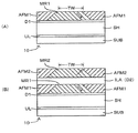
図1(A)は、第1の磁気抵抗ストライプ(first MR stripe) MR1から始まるDSMR素子10の製造の第1の段階を表すものである。通常のように、DSMR素子10は平坦な基板SUB上に形成する。まず、基板SUB上に、順に、平坦な下地層UL、下地層ULを覆う平坦な磁気シールド層SH、およびその上の平坦な絶縁層(誘電体層;dielectric layer)D1を形成する。次に、第1の磁気抵抗ストライプMR1を絶縁層D1の表面上に従来の方法で形成する。第1の磁気抵抗ストライプMR1は、好ましくは、パーマロイ(NiFe:ニッケル−鉄)またはCoFeまたはCoNiFeを用いて形成し、その横方向の端部が外向きのテーパ形状をなすようにする。具体的には、上端に向かって狭まり下端に向かって広がる台形状の断面パターンを有する。ここで、絶縁層D1の側が最も広くなっている。
【0021】
次に、第1の磁気抵抗ストライプMR1の外向きのテーパ形状をなす横方向の両端部に、1対の第1の反強磁性構造AFM1を形成する。好ましくは、第1の反強磁性構造AFM1は、MnPt(白金−マンガン),NiMn(ニッケル−マンガン),またはMnPdPt(白金−パラジウム−マンガン)のようなブロッキング温度の高い材料で構成されている。1対の第1の反強磁性構造AFM1の相互の間隔がトラック幅TWとなる。
【0022】
次に、DSMR素子10に対して、約250°Cから約300°Cという範囲の高い温度(好ましくは約280°C)の下で、かつ、約1000×10 3 /4π[A/m](から約2000×10 3 /4π[A/m]という範囲の強い外部磁界下において、約5時間、第1の(最初の)磁気アニール工程を行う。
【0023】
図1(B)は、図1(A)に示したDSMR素子10の製造工程における第2の段階が終了した後の状態を表すものである。まず、第1の段階として、図1(A)のDSMR素子10の表面上に、平坦かつ電気的絶縁性を有する平坦絶縁層ILAを成膜する。平坦絶縁層ILAは、非磁性かつ絶縁性の、例えばアルミナ(酸化アルミニウム(Al2 O3 )、窒化アルミニウム(AlN)、および酸化ケイ素(SiO2 )の少なくとも1つを用いて形成する。このとき、平坦絶縁層ILAは、第1の磁気抵抗ストライプMR1の上面と、第1の磁気抵抗ストライプMR1の上端と同一平面上にあるように図示されている1組の第1の反強磁性構造AFM1の上面とを覆うようにする。
【0024】
次に、平坦絶縁層ILAの平坦な上面に、第2の磁気抵抗ストライプMR2を成膜する。さらに、第2の磁気抵抗ストライプMR2の端部に、1組の第2の反強磁性構造AFM2を形成する。このとき、第2の磁気抵抗ストライプMR2もまた、その横方向の端部が外向きのテーパ形状をなすようにする。つまり、上端に向かって狭まり絶縁性の層ILA側の下端に向かって広がるようにする。第2の反強磁性構造AFM2は、MnPt,NiMn,MnPdPtのような第1の反強磁性構造AFM2の場合と同じ材料、またはIrMn(イリジウム−マンガン),FeMn(鉄−マンガン),もしくはNiO(酸化ニッケル)のような不規則系材料で構成することが好ましい。
【0025】
次に、第1の反強磁性層AFM1の存在下で第2の反強磁性層AFM2を安全に形成(すなわち、リセット)するために、第2の(中間の)アニール工程を行う。ここで、重要なことは、第1の反強磁性層AFM1が依然安定であるような(すなわち、磁化方向が変化しないような)弱いアニール磁界(Hann )および適切な温度を選ぶことである。ここで、弱いアニール磁界(Hann )とは、アニール時において印加される外部磁界であって、第1の反強磁性層AFM1の交換磁界Hex(T)よりも小さい磁界を意味する。
【0026】
第2のアニール工程では、DSMR素子10に対して、例えば、約200°Cから約260°Cという範囲の温度(好ましくは約250°C)の下で、約100×10 3 /4π[A/m]から約300×10 3 /4π[A/m]という範囲の弱い外部磁界(Hann )(好ましくは約250×10 3 /4π[A/m])を印加して、約2時間から約5時間の範囲の継続時間をもって、第2の磁気アニール処理を行う。
【0027】
第3の(そして最後の)アニール工程では、まず第2の反強磁性層AFM2の交換磁界(Hex)(これは、第1の反強磁性層AFM1の交換磁界(Hex)ほど強くはないが)を生じさせた後、外部から磁界を印加しない状態で(Hann =0)、高温のアニール工程を行い、第2の反強磁性層の交換磁界(Hex)を、その全強度まで増加させる。このアニール工程はまた、第1の反強磁性層の安定性をもさらに向上させる。すなわち、第1の反強磁性層の交換磁界(Hex)は、たとえそれが( 第2のアニール工程における) 弱い磁界下でのアニール処理によって低下していたとしても、第3のアニール工程によって再び増加するのである。
【0028】
第3のアニール工程では、例えば、約250°Cから約300°Cという範囲の高い温度(好ましくは約260°C)の下で、約5時間から約10時間という継続時間をもって、DSMR素子10に対して、外部磁界を印加しない(Hann =0)アニール(第3のアニール処理)を行う。
【0029】
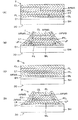
図2(A)は、SVMR形素子30の上部SVMR構造Tを製造する工程における第1の段階を表すものである。通常のように、SVMR形素子30は平坦なシールド層SH上に形成する。具体的には、まず、シールド層SHの上に、順に、絶縁層D1,金属の基層BL、基層BLを覆う軟磁性(soft FerroMagnetic)のフリー層FL、および平坦な導電体層C1を形成する。基層BLは、例えば、タンタル(Ta),ジルコニウム(Zr),コバルト−ジルコニウム−ニオブ(CoZrNb),パーマロイ((Ni80Fe20)60Cr40,等)で構成するのが好ましい。軟磁性のフリー層FLは、例えば、パーマロイ(Ni80Fe20、すなわち、ニッケル:鉄=80:20)、NiFe/CoFe、またはNiFe/Coのような、合金の複合層で構成するのが好ましい。平坦な導電体層C1の形成には、例えば、銅(Cu)または金(Au)のような金属を用い、その上面が平坦になるようにする。
【0030】
次に、銅(Cu)または金(Au)の導電体層C1の平坦な上面の上に、強磁性を有する複合体である平坦な磁化方向固定層(a pinned layer)PILを形成する。磁化方向固定層PILは、コバルト(Co)、コバルトと鉄との合金(CoFe)、またはNiFe/CoFeもしくはNiFe/Coのような合金で構成するのが好ましい。但し、ニッケル鉄(NiFe)合金(例えばパーマロイ)は、相互拡散という製錬上の問題を有しているので、銅と直接接触する場合には適当ではない。したがって、銅を用いる場合には、上記のような製錬上の問題に対処するために、Cu/CoFe/AFM,Cu/Co/AFM,Cu/CoFe/NiFe/AFM,またはCu/Co/NiFe/AFM等のような多層構造にすることが好ましい。
【0031】
次に、強磁性を有する磁化方向固定層PILの平坦な上面の上に、平坦な第1の反強磁性層AFMAを形成する。第1の反強磁性層AFMAは、MnPt,MnPdPt,またはNiMnのようなブロッキング温度の高い材料で構成するのが好ましい。
【0032】
次に、第1の反強磁性層AFMAの平坦な上面の上に、タンタルなどの金属からなるキャップ層CLを形成する。
【0033】
次に、SVMR形素子30に対して、第1の(最初の)磁気アニール工程を行う。この工程は、約250°Cから約300°Cという範囲の高い温度(好ましくは約280°C) の下で、図2(A)の矢印で示した方向に約1000×10 3 /4π[A/m]から約2000×10 3 /4π[A/m]という範囲の強い外部磁界(Hann1)(好ましくは、約2000×10 3 /4π[A/m]) を印加した状態で行う。
【0034】
第2の製造段階においては、図2(B)に示したように、通常のエッチング処理により、図2(A)のSVMR形素子30の上部SVMR構造Tを、その側壁がテーパ形状をなすようにパターニングする。具体的には、上部SVMR構造Tの断面形状が、フリー層FLが最も広くキャップ層CLが最も狭い台形状になるようにする。
【0035】
次に、これらの側壁に、強磁性層( 縦方向における磁化方向固定層;longitudinal pinned layer) LPを形成する。これにより、強磁性層LPは、縦方向(図2(B)における左右方向)において、SVMR形素子30の左右のテーパ付けされた側壁を覆う。すなわち、強磁性層LPによって、金属からなる基層BL、フリー層FL、導電体層C1、磁化方向固定層PIL、第1の反強磁性層AFMAおよびキャップ層CLの両端面が覆われる。強磁性層LPは、Co,CoFe,またはNiFe等の材料で構成するのが好ましい。
【0036】
次に、強磁性層(縦方向における磁化方向固定層)LPの上に、テーパ形状をなす両側壁(すなわち、SVMR形素子30の左右のテーパ側壁) を覆うように、第2の反強磁性層AFMBを積層する。これにより、第2の反強磁性層AFMBがSVMR形素子30の左右に形成される。
【0037】
第2の反強磁性構造AFMBは、MnPt,NiMn,MnPdPtのような規則系の反強磁性材料、または、IrMn,FeMnもしくはNiOのような不規則系の材料で構成することが好ましい。
【0038】
図2(C)は、SVMR形素子30の下部SVMR構造Bを製造する工程における第1の段階が完了した状態を表すものである。下部SVMR構造Bは、上記の図2(A)に示した上部SVMR素子Tと同様の方法で形成される。
【0039】
図2(D)は、SVMR形素子30の下部SVMR構造Bの製造工程における第2の段階が完了した状態を表すものである。下部SVMR構造Bは、図2(B)に示した上部SVMR素子Tと同様の方法で形成される。
【0040】
第2のアニール工程では、上部SVMR構造Tと下部SVMR構造Bとを含むSVMR形素子30に対して、弱い第2のアニール磁界(Hann2)の下で、第2の磁気アニール処理を行う。具体的には、例えば、約200°Cから約260°Cの範囲の温度(好ましくは、約250°C) の下で、約100×10 3 /4π[A/m]から約300×10 3 /4π[A/m]の範囲の弱い外部アニール磁界(Hann2)(好ましくは約250×10 3 /4π[A/m]) を印加して、SVMR形素子30のアニール処理を行う。
【0041】
第3の( そして最後の) アニール工程では、まず第2の反強磁性層AFMBの交換磁界(Hex)(これは、第1の反強磁性層AFMAの交換磁界(Hex)ほど強くはないが)を生じさせた後、外部から磁界を印加しない状態で(Hann =0)、高温のアニール工程を行い、第2の反強磁性層の交換磁界(Hex)を、その全強度まで増加させる。このアニール工程はまた、第1の反強磁性層の安定性をもさらに向上させる。すなわち、第1の反強磁性層の交換磁界(Hex)は、たとえそれが( 第2のアニール工程における) 弱い磁界アニール処理によって低下していたとしても、第3のアニール工程によって再び増加するのである。
【0042】
第3のアニール工程では、例えば約250°Cから約300°Cという範囲の高い温度(好ましくは約270°C)で、SVMR形素子30に対して、外部磁界を印加しない(Hann3=0)アニール(第3のアニール処理)を行う。
【0043】
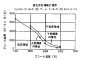
図3は、下部SVMR構造B(AFM/FM構造) に対する上部SVMR構造T(FM/AFM構造) の熱安定性が第2の垂直なアニール磁界(Hann2)およびアニール温度にどのように依存するかを示す磁化安定領域境界(the Boundary of the M-Stable Region) を表す図である。ここで、AFM/FMという表記は、反強磁性層(AFM)の上に強磁性層(FM)を積層した構造であることを意味し、FM/AFMという表記は、強磁性層(FM)の上に反強磁性層(AFM)を積層した構造であることを意味する。本明細書の他の箇所においても同様である。なお、この図3に示した例では、AFM/FM構造として、Ta/MnPt(20nm)/CoFe(3nm)/Taという積層構造を用い、FM/AFM構造として、Cu/CoFe(3nm)/MnPt(20nm)/Taという積層構造を用いた。括弧内の数字は膜厚を表す。これらの2つの試料は、最初に高温かつ強磁界(例えば280°C×5時間×2000×10 3 /4π[A/m])でアニールされた。ここで、磁化安定領域境界は、アニール磁界および温度の値の各組合せごとに、12時間アニールを行った後、試料の磁化固定方向を最初のアニール方向に対して5度回転させるようにして行った場合のものとして定義した。
【0044】
図4は、温度250°C,2000×10 3 /4π[A/m]の強磁界下で5時間アニールした後、交換結合(exchange coupling) が完全に成立したNiFe(3nm)/CoFe(5nm)/MnPt(25nm)/Taについて、測定温度に対する交換磁界Hexを表したものである。
【0045】
図5は、弱磁界(30×10 3 /4π[A/m])の存在下で、第2の反強磁性層(SVMR形素子30における第2の反強磁性層AFMBに相当)を250°Cで5時間アニールした後のNiFe(3nm)/CoFe(5nm)/MnPt(25nm)/Taについて、測定温度に対する交換磁界Hexを表したものである。この条件下では、隣接する第1の反強磁性層(既に形成されている第1の反強磁性層AFMAに相当)に対する影響はなかった。
【0046】
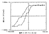
図6〜図10は、NiFe/NiMnについての5通りの異なるM−H(Magnetization-Magnetic Field;磁化−磁界)ループを表すものである。このうち、図6は、NiFe(11nm)/NiMn(30nm)/Taという積層構造のサンプルを、温度300°C, 2000×10 3 /4π[A/m]の磁界下で5時間アニールしたときのM−Hループを表す。
【0047】
図7は、NiFe(11nm)/NiMn(30nm)/Taという積層構造のサンプルを、温度260°C, 260×10 3 /4π[A/m]の弱い外部磁界下で1時間アニールした場合のM−Hループを表す。
【0048】
図8は、NiFe(11nm)/NiMn(30nm)/Taという積層構造のサンプルを、最初に図6に示した条件でアニールしたのち、アニール磁界方向を最初の逆にして、温度260°C, 260×10 3 /4π[A/m]の弱い外部磁界下で1時間再アニールした場合のM−Hループを表す。
【0049】
図9は、NiFe(11nm)/NiMn(30nm)/Taという積層構造のサンプルを、図6および図8に示した条件でアニールしたのち、外部磁界を印加せずに温度280°Cで3時間再アニールした場合のM−Hループを表す。この図9から、低下した交換磁界Hex(図8参照)が回復していることが分かる。
【0050】
図10は、NiFe(11nm)/NiMn(30nm)/Taという積層構造のサンプルを、図7に示したようにアニールしたのち、外部磁界を印加せずに温度280°Cで3時間再アニールした場合のM−Hループを表す。この図10から分かるように、交換磁界Hex(図8参照)の強度はさらに向上している。
【0051】
本実施の形態に係る磁気抵抗構造の製造方法および磁気抵抗型ヘッドの製造方法の要点は、以下の通りである。
(1)本処理の結果、最初に形成された反強磁性層に対して、熱による外部からの影響はない。
(2)第1の反強磁性層および第2の反強磁性層の磁化固定方向をリセットすることが簡単である。
(3)本方法では、隣接する第1の反強磁性層(第1の磁化固定層)の磁化安定性を維持しつつ、第2の反強磁性層における反強磁性材料の相を形成することができるような、弱いアニール磁界Hann ,適度の温度Tおよび適切なアニール時間tann を選ぶこと、すなわち、(H,T,tann )<(H,T,tann ) c とすることが重要である。
(4)第1および第2の反強磁性層の安定性と交換磁界Hexとを向上させるために、最後に、外部磁界を印加しない(Hann =0)第3のアニール工程を高温で行うようにしている。
(5)第1の反強磁性層には、ブロッキング温度の高い反強磁性材料を用いるのが好ましい。
(6)DSMRおよびSVMRヘッドの用途においては、第2の磁気抵抗層の磁化方向を好ましい方向に固定するために(DSMRの場合)、またはフリー層( センス層) の磁化方向を縦方向に沿って固定するために(SVMRの場合)、第2の反強磁性層が必要となる。第2の反強磁性層の形成条件は、既に形成された第1の反強磁性層に劣化(交換磁界の減少や回転容易軸の回転)が生じないように選ばれるべきである。第1および第2の反強磁性材料は同じであってもよいが、異なっていてもよい。第1および第2の反強磁性材料を同じくする場合には、例えば、MnPt/MnPt,MnPdPt/MnPdPt,もしくはNiMn/NiMnという組み合わせとするのが好ましい。一方、第1および第2の反強磁性材料を異ならせる場合には、例えば、MnPt/FeMn,MnPdPt/FeMn,NiMn/FeMn,MnPt/IrMn,MnPdPt/IrMn,NiMn/IrMn,MnPt/NiO,MnPt/FeMn,MnPdPt/FeMn,およびNiMn/FeMn等の組み合わせとするのが好ましい。
【0052】
以上、具体的な実施の形態を挙げて本発明を説明したが、本発明が冒頭に記載された請求項の精神および範囲内で変形して実施可能であること、すなわち、本発明の精神および範囲を逸脱することなく形式および詳細に関わる変更をなしうることは明らかである。したがって、そのような変更はすべて本発明の範囲内に含まれるものであり、本発明は冒頭に記載された請求項の主題を包含するものである。
【0053】
【発明の効果】
以上説明したように、本発明によれば、既に形成されている第1の反強磁性層に影響(外部磁界や熱による外部からの影響)を及ぼすことなく、あとから形成する第2の反強磁性層を、第1の反強磁性層と同一または異なる材料により形成することが可能である。また、第1の反強磁性層および第2の反強磁性層の磁化固定方向をリセットすることが容易である。
【図面の簡単な説明】
【図1】本発明の一実施の形態に係るDSMR素子の製造工程を表す断面図である。
【図2】本発明の一実施の形態に係るSVMR素子の製造工程を表す断面図である。
【図3】図2に示した上部SVMR構造および下部SVMR構造の熱安定性と第2の垂直なアニール磁界およびアニール温度との依存関係を表す磁化安定領域境界を表す図である。
【図4】 強磁界下でアニールされ、その後交換結合が完全に成立したNiFe(3nm)/CoFe(5nm)/MnPt(25nm)/Taについて、測定温度に対する交換磁界Hexを表す図である。
【図5】 隣接する第1の反強磁性層に影響を及ぼさない弱磁界の存在下で第2の反強磁性層をアニールした後のNiFe(3nm)/CoFe(5nm)/MnPt(25nm)/Taについて、測定温度に対する磁界Hexを表す図である。
【図6】 2000Oeで5時間、300°CでアニールされたNiFe(11nm)/NiMn(30nm)/Taについて、M−Hループを表す図である。
【図7】 260×10 3 /4π[A/m]の弱い外部磁界下で1時間、260°CでアニールされたNiFe(11nm)/NiMn(30nm)/Ta試料について、M−Hループを表す図である。
【図8】 最初に図6に示した条件でアニールされ、次に反対のアニール方向で弱い外部磁界下で再アニールされたNiFe(11nm)/NiMn(30nm)/Taについて、M−Hループを表す図である。
【図9】 図6および図8に示した条件でアニールし、次に外部磁界を印加せずに再アニールした後のNiFe(11nm)/NiMn(30nm)/Ta試料について、M−Hループを表す図である。
【図10】 図7に示したようにアニールし、次に外部磁界を印加せずに再アニールした後のNiFe(11nm)/NiMn(30nm)/Taについて、M−Hループを表す図である。
【符号の説明】
10…DSMR素子、SUB…基板、UL…下地層、SH…磁気シールド層、D1…絶縁層、MR1…第1の磁気抵抗ストライプ、MR2…第2の磁気抵抗ストライプ、AFM1…第1の反強磁性構造、AFM2…第2の反強磁性構造、TW…トラック幅、ILA…平坦絶縁層、30…SVMR形素子、T…上部SVMR構造、B…下部SVMR構造、BL…基層、FL…フリー層、C1…導電体層、PIL…磁化方向固定層、AFMA…第1の反強磁性層、AFMB…第2の反強磁性層、LP…(縦方向に磁化方向が固定された)磁化方向固定層、CL…キャップ層。[0001]
BACKGROUND OF THE INVENTION
The present invention provides a magnetoresistiveeffectElement (or magnetoresistanceeffectMagnetoresistance with sensoreffectStructure manufacturing method and this magnetoresistanceeffectMagnetoresistance constructed using elementseffectThe present invention relates to a mold head manufacturing method.Hereinafter, the “magnetoresistance effect” is abbreviated as “magnetoresistance”.
[0002]
[Prior art]
Voegeli et al., US Pat. No. 5,561,896, “Method for Manufacturing Magnetoresistive Transducer” discloses a method called SPI (Selective Pulse Interdiffusion) method. This SPI method is a method of selectively heating a region for forming a bias portion of a magnetoresistive (MR) head using one or a plurality of current pulses (hereinafter referred to as short current pulses) having a short pulse width. It is. This magnetoresistive head is configured using a transducer that converts a magnetic signal into an electric signal. As this transducer, an MR element having an H-shaped structure is used. The portion corresponding to the “H” horizontal bar in this MR element is an active central region made of a soft magnetic layer. The short current pulse described above passes through the “H” side legs of the MR element, and anneals / resets the soft magnetic layer to change the “H” legs into a hard magnetic material. Thus, a soft magnetic layer (for example, Permalloy (trade name)) and titanium (Ti), tantalum (Ta), chromium (Cr), or other transition metal or refractory metal composed of each other. Interdiffusion occurs between the diffusion layers.
[0003]
Gill US Pat. No. 5,748,399 “Resettable symmetric spin valve” uses an anti-ferromagnetic (AFM) layer above its blocking temperature using a short current pulse passing through a conductor. Describes an annealing method for heating.
[0004]
In U.S. Pat. No. 5,772,794 “Method of manufacturing magnetic head / device having spin valve effect magnetoresistive head”, two thin film layers made of soft magnetic material are used. A laminated body is described which is separated and laminated by a thin film layer made of a magnetic material. One of the two thin film layers (first and second thin film layers) has a magnetization direction pinned by a thin film antiferromagnetic layer. After forming the two thin film layers, the laminated body is annealed to generate uniaxial anisotropy in the soft magnetic layer whose magnetization direction is fixed.
[0005]
Ohtsuka et al. US Pat. No. 5,859,753 “Spin-valve magnetoresistive head with spin valves connected in series” uses a plurality of antiferromagnetic layers with different blocking temperatures using only two annealing steps. A spin valve magnetoresistive head formed in this manner is disclosed. This head has two magnetization direction pinning layers composed of antiferromagnetic layers and having magnetization directions antiparallel to each other. One of them is NiMn having a high blocking temperature, and the other layer is FeMn having a low blocking temperature. From the 10th column to the 19th column of the 10th column, “... on the first magnetization direction fixed layer .... at a temperature of 200 ° C. to 300 ° C .... NiMn having a high blocking temperature is Formed as a ferromagnetic layer, this NiMn is a magnetic field H applied in the first direction01Formed under. Thereafter, ... FeMn is formed as a second antiferromagnetic layer on the second magnetization direction pinned layer ... at a temperature around 160.degree. The formation of FeMn is caused by the magnetic field H in the direction opposite to the first direction.02Is carried out while applying. "a. Further, it is pointed out that another method can be used from the 37th column to the 60th column of the 10th column. Specifically, the magnetic field H is heated to a high blocking temperature.01And the subsequent heating to a low blocking temperature and the magnetic field H02It is described that the step of applying can be delayed until after these antiferromagnetic layers are formed.
[0006]
US Pat. No. 5,856,897 to Mauri “Self-biased dual spin valve” includes a magnetic layer whose magnetization direction is not fixed between two magnetic layers (pinned layers) whose magnetization direction is fixed. A dual spin valve (DSV) magnetoresistive sensor having a (free magnetic layer) is disclosed.
[0007]
[Problems to be solved by the invention]
When using an exchange coupling method in a dual stripe magnetoresistive (hereinafter referred to as “DSMR”) head or a spin valve magnetoresistive (hereinafter referred to as “SVMR”) head, In order to fix the two magnetoresistive layers in the preferred direction (in the case of DSMR) or in order to fix the free layer (sense layer) in the vertical direction (direction in which the sense current flows) (in the case of SVMR), the second An antiferromagnetic layer is required. However, conventionally, it has not always been easy to appropriately form such a second antiferromagnetic layer without impairing necessary magnetic properties.
[0008]
The present invention has been made in view of such a problem. For example, in a DSMR head or an SVMR head, the second antiferromagnetic layer to be formed later is used as a first (already formed) first layer. To provide a magnetoresistive structure manufacturing method and a magnetoresistive head manufacturing method including a new thermal annealing method that can be formed of the same or different materials without affecting the antiferromagnetic layer. .
[0009]
[Means for Solving the Problems]
The present invention affects the first antiferromagnetic layer and the first annealing step for forming the first antiferromagnetic layer (a first AFM layer) in the DSMR head and the SVMR head. A second annealing step for resetting the second antiferromagnetic layer (a second AFM layer) without applying a magnetic field from the outside (Hann= 0), and by performing the annealing at a high temperature (than the annealing temperature in the second annealing step), the reduced exchange field of the first antiferromagnetic layer is restored and the second antiferromagnetic layer is restored. And a third annealing step for improving the exchange magnetic field. In this specification, two elements made of antiferromagnetic material are expressed as first and second antiferromagnetic layers, but more generally expressed as first and second antiferromagnetic elements. Of course, you may.
[0010]
As described above, when the second magnetoresistive layer is fixed in a preferred direction in the DSMR head employing the exchange coupling method, the free layer (sense layer) is biased in the vertical direction (the direction in which the sense current flows) in the SVMR head. In the case of fixing, a second antiferromagnetic layer is required in addition to the first antiferromagnetic layer. The present invention allows these first and second antiferromagnetic layers to be made of the same or different materials (eg, MnPt / MnPt, MnPdPt / MnPdPt without affecting the first (existing) antiferromagnetic layer). , NiMn / NiMn, or MnPt / IrMn, MnPdPt / IrMn, NiMn / IrMn,...).
[0011]
According to the present invention, the magnetoresistance is as follows:effectA method for manufacturing a mold head is provided. First, magnetoresistance having a first antiferromagnetic layereffectMagnetoresistance including elementseffectForm a structure. continue,FirstUnder magnetic fieldOf the first temperatureThe first annealing stepOver the first timeDo. Next, the remaining magnetoresistance including the second antiferromagnetic layereffectForm a structure. And following the formation of the second antiferromagnetic layer,Second weaker than the first magnetic fieldMagnetic field (HannUnderA second temperature lower than the first temperatureAnnealing processOver the second timeDo. Then, in a state where no magnetic field is applied from the outside (Hann= 0),3rd temperature higher than 2nd temperatureAnnealing processOver the third timeDo and secondExchange couplingMagnetic field (Hex)IncreaseLet me add. This also improves the stability of the first antiferromagnetic layer. That is, the first antiferromagnetic layer (generated in the first annealing step)First exchange coupling inMagnetic field (Hex) Even if it is under a weak magnetic fieldSecond annealing stepEven if it drops in, it increases and is repaired.
[0012]
According to another aspect of the present invention, a magnetoresistive structure having a magnetoresistive element is formed to include a pinned layer and a first antiferromagnetic layer.
[0013]
The magnetization direction fixed layer is preferably the following layer.
(1) a single soft magnetic material selected from the group consisting of NiFe, Co, CoFe, and CoNiFe, or
(2) NiFe / CoFe, NiFe / Co, CoFe / NiFe, Co / NiFe, CoNiFe / NiFe, NiFe / CoNiFe, CA composite of soft magnetic materials selected from the group consisting of o / CoNiFe, CoNiFe / Co, CoFe / Co, and Co / CoFe.
[0014]
The first antiferromagnetic layer is preferably made of a material having a high blocking temperature, and more preferably made of a material having a higher blocking temperature than at least the second antiferromagnetic layer.
[0015]
The first and second antiferromagnetic layers are preferably composed of material layers as shown in the following (1) or (2).
(1) An antiferromagnetic material layer selected from the group consisting of a combination of ordered / ordered antiferromagnetic material layers consisting of MnPt / MnPt, NiMn / NiMn, and MnPdPt / MnPdPt.
(2) Regular system / disorder consisting of MnPt / FeMn, MnPdPt / FeMn, NiMn / FeMn, MnPt / IrMn, MnPdPt / IrMn, NiMn / IrMn, MnPt / NiO, MnPt / FeMn, MnPdPt / FeMn, and NiMn / FeMn An antiferromagnetic material layer selected from the group of combinations of antiferromagnetic material layers.
[0016]
DETAILED DESCRIPTION OF THE INVENTION
Hereinafter, embodiments of the present invention will be described in detail with reference to the drawings.
[0017]
In the application of DSMR and SVMR recording heads, when the exchange coupling method is adopted, in order to fix the magnetization direction of the second magnetoresistive layer (which will be formed later in the manufacturing process) in a preferred direction (in the case of DSMR) ), Or a second antiferromagnetic layer is required to bias the magnetization direction of the free layer (sense layer) along the longitudinal direction (in the case of SVMR).
[0018]
The condition for forming the second antiferromagnetic layer on the first antiferromagnetic layer is that the first antiferromagnetic layer formed earlier deteriorates, for example, the exchange magnetic field HexShould be chosen so that there is no decrease in rotation or rotation of the unstable axis (easy axis).
[0019]
In this embodiment, regardless of whether the first and second antiferromagnetic layers are made of the same material or different materials, the second antiferromagnetic layer is not affected. The present invention provides a new thermal annealing method capable of forming an antiferromagnetic layer.
[0020]
FIG. 1A represents a first stage of manufacture of a
[0021]
Next, a pair of first antiferromagnetic structures AFM1 are formed at both lateral ends of the first magnetoresistive stripe MR1 that form an outwardly tapered shape. Preferably, the first antiferromagnetic structure AFM1 is made of a material having a high blocking temperature, such as MnPt (platinum-manganese), NiMn (nickel-manganese), or MnPdPt (platinum-palladium-manganese). The distance between the pair of first antiferromagnetic structures AFM1 is the track width TW.
[0022]
Next, for the
[0023]
FIG. 1B shows a state after the second stage in the manufacturing process of the
[0024]
Next, a second magnetoresistive stripe MR2 is formed on the flat upper surface of the flat insulating layer ILA. Further, a pair of second antiferromagnetic structures AFM2 is formed at the end of the second magnetoresistive stripe MR2. At this time, the second magnetoresistive stripe MR2 is also configured such that its lateral end has an outwardly tapered shape. That is, it narrows toward the upper end and widens toward the lower end on the insulating layer ILA side. The second antiferromagnetic structure AFM2 is the same material as the first antiferromagnetic structure AFM2 such as MnPt, NiMn, MnPdPt, or IrMn (iridium-manganese), FeMn (iron-manganese), or NiO ( It is preferable to use an irregular material such as nickel oxide).
[0025]
Next, a second (intermediate) annealing step is performed to safely form (ie, reset) the second antiferromagnetic layer AFM2 in the presence of the first antiferromagnetic layer AFM1. Here, the important thing is that the first antiferromagnetic layer AFM1 is still stable (that is, the magnetization direction does not change), a weak annealing magnetic field (Hann) And choosing an appropriate temperature. Here, weak annealing magnetic field (Hann) Is an external magnetic field applied during annealing, and the exchange magnetic field H of the first antiferromagnetic layer AFM1exIt means a magnetic field smaller than (T).
[0026]
In the second annealing step, the
[0027]
In the third (and final) annealing step, first, the exchange magnetic field (H of the second antiferromagnetic layer AFM2)ex(This is the exchange magnetic field (H of the first antiferromagnetic layer AFM1)ex) But not as strong) and after applying no magnetic field (Hann= 0), a high temperature annealing step is performed, and the exchange magnetic field (Hex) To its full strength. This annealing step also further improves the stability of the first antiferromagnetic layer. That is, the exchange magnetic field (H of the first antiferromagnetic layer)ex) Is increased again by the third annealing step, even though it has been reduced by the annealing treatment under a weak magnetic field (in the second annealing step).
[0028]
In the third annealing step, for example, the
[0029]
FIG. 2A shows a first stage in the process of manufacturing the upper SVMR structure T of the
[0030]
Next, a flat pinned layer PIL, which is a composite having ferromagnetism, is formed on the flat upper surface of the copper (Cu) or gold (Au) conductor layer C1. The magnetization direction fixed layer PIL is preferably made of cobalt (Co), an alloy of cobalt and iron (CoFe), or an alloy such as NiFe / CoFe or NiFe / Co. However, a nickel iron (NiFe) alloy (for example, permalloy) has a problem in smelting called interdiffusion, and thus is not suitable for direct contact with copper. Therefore, when using copper, Cu / CoFe / AFM, Cu / Co / AFM, Cu / CoFe / NiFe / AFM, or Cu / Co / NiFe are used to cope with the above-mentioned smelting problems. A multilayer structure such as / AFM is preferable.
[0031]
Next, a flat first antiferromagnetic layer AFMA is formed on the flat upper surface of the magnetization direction fixed layer PIL having ferromagnetism. The first antiferromagnetic layer AFMA is preferably composed of a material having a high blocking temperature such as MnPt, MnPdPt, or NiMn.
[0032]
Next, a cap layer CL made of a metal such as tantalum is formed on the flat upper surface of the first antiferromagnetic layer AFMA.
[0033]
Next, a first (first) magnetic annealing step is performed on the
[0034]
In the second manufacturing stage, as shown in FIG. 2B, the sidewall of the upper SVMR structure T of the
[0035]
Next, on these side walls,strengthA magnetic layer (longitudinal pinned layer) LP is formed. ThisstrengthThe magnetic layer LP covers the left and right tapered sidewalls of the
[0036]
next,strengthOn the magnetic layer (magnetization direction pinned layer) LP, a second antiferromagnetic layer AFMB is laminated so as to cover both side walls having a tapered shape (that is, the left and right tapered side walls of the SVMR element 30). To do. As a result, the second antiferromagnetic layer AFMB is formed on the left and right sides of the
[0037]
The second antiferromagnetic structure AFMB is preferably composed of an ordered antiferromagnetic material such as MnPt, NiMn, or MnPdPt, or an irregular material such as IrMn, FeMn, or NiO.
[0038]
FIG. 2C shows a state where the first stage in the process of manufacturing the lower SVMR structure B of the
[0039]
FIG. 2D shows a state in which the second stage in the manufacturing process of the lower SVMR structure B of the
[0040]
In the second annealing step, a weak second annealing magnetic field (H) is applied to the
[0041]
In the third (and final) annealing step, first, the exchange magnetic field (H of the second antiferromagnetic layer AFMB)ex(This is the exchange magnetic field (H of the first antiferromagnetic layer AFMA)ex) But not as strong) and after applying no magnetic field (Hann= 0), a high temperature annealing step is performed, and the exchange magnetic field (Hex) To its full strength. This annealing step also further improves the stability of the first antiferromagnetic layer. That is, the exchange magnetic field (H of the first antiferromagnetic layer)ex) Is increased again by the third annealing step even though it has been reduced by the weak magnetic field annealing treatment (in the second annealing step).
[0042]
In the third annealing step, an external magnetic field is not applied to the
[0043]
FIG. 3 shows that the thermal stability of the upper SVMR structure T (FM / AFM structure) with respect to the lower SVMR structure B (AFM / FM structure)ann2) And the magnetization stable region boundary (the Boundary of the M-Stable Region) showing how it depends on the annealing temperature. Here, the notation AFM / FM means a structure in which a ferromagnetic layer (FM) is laminated on an antiferromagnetic layer (AFM), and the notation FM / AFM means a ferromagnetic layer (FM). It is a structure in which an antiferromagnetic layer (AFM) is laminated on the substrate. The same applies to other portions of the present specification. In the example shown in FIG. 3, Ta / MnPt (AFM / FM structure)20nm) / CoFe (3nm) / Ta, and the FM / AFM structure is Cu / CoFe (3nm) / MnPt (20nm) / Ta stacked structure was used. The numbers in parentheses are membranesThicknessTo express. These two samples are initially high temperature and strong magnetic fields (eg 280 ° C. × 5 hours × 2000× 10 3 / 4π [A / m]). Here, the magnetization stable region boundary is obtained by performing 12 hours of annealing for each combination of the annealing magnetic field and temperature value, and then rotating the magnetization fixing direction of the sample by 5 degrees with respect to the initial annealing direction. Defined as the case.
[0044]
FIG. 4 shows a temperature of 250 ° C. and 2000× 10 3 / 4π [A / m]After 5 hours of annealing in a strong magnetic field, NiFe (exchange coupling) is completely established (3nm) / CoFe (5nm) / MnPt (25nm) / Ta, exchange magnetic field H for measured temperatureexIt represents.
[0045]
FIG. 5 shows a weak magnetic field (30× 10 3 / 4π [A / m]) After annealing the second antiferromagnetic layer (corresponding to the second antiferromagnetic layer AFMB in the SVMR element 30) at 250 ° C. for 5 hours.3nm) / CoFe (5nm) / MnPt (25nm) / Ta, exchange magnetic field H for measured temperatureexIt represents. Under this condition, there was no effect on the adjacent first antiferromagnetic layer (corresponding to the already formed first antiferromagnetic layer AFMA).
[0046]
FIGS. 6 to 10 represent five different MH (Magnetization-Magnetic Field) loops for NiFe / NiMn. Among these, FIG. 6 shows NiFe (11nm) / NiMn (30nm) / Ta sample having a laminated structure at a temperature of 300 ° C, 2000× 10 3 / 4π [A / m]Represents an MH loop when annealed for 5 hours under a magnetic field of.
[0047]
FIG. 7 shows NiFe (11nm) / NiMn (30nm) / Ta samples with a laminated structure at temperatures of 260 ° C and 260 ° C.× 10 3 / 4π [A / m]Represents an MH loop when annealed for 1 hour under a weak external magnetic field.
[0048]
FIG. 8 shows NiFe (11nm) / NiMn (30nm) / Ta is first annealed under the conditions shown in FIG. 6, and the annealing magnetic field direction is first reversed, and the temperature is 260 ° C., 260× 10 3 / 4π [A / m]Represents an MH loop when re-annealed for 1 hour under a weak external magnetic field.
[0049]
FIG. 9 shows NiFe (11nm) / NiMn (30nm) / Ta represents a MH loop when a sample having a laminated structure is annealed under the conditions shown in FIGS. 6 and 8 and then reannealed at a temperature of 280 ° C. for 3 hours without applying an external magnetic field. From FIG. 9, it can be seen that the exchange field H has been lowered.exIt can be seen that (see FIG. 8) has recovered.
[0050]
FIG. 10 shows NiFe (11nm) / NiMn (30nm) / Ta represents a MH loop in which a sample having a laminated structure is annealed as shown in FIG. 7 and then reannealed at a temperature of 280 ° C. for 3 hours without applying an external magnetic field. As can be seen from FIG. 10, the exchange magnetic field HexThe strength of (see FIG. 8) is further improved.
[0051]
The main points of the magnetoresistive structure manufacturing method and the magnetoresistive head manufacturing method according to the present embodiment are as follows.
(1) As a result of this treatment, the antiferromagnetic layer formed first is not affected by heat from the outside.
(2) It is easy to reset the magnetization fixed directions of the first antiferromagnetic layer and the second antiferromagnetic layer.
(3) In this method, the phase of the antiferromagnetic material in the second antiferromagnetic layer is formed while maintaining the magnetization stability of the adjacent first antiferromagnetic layer (first magnetization fixed layer). Weak annealing magnetic field Hann, Moderate temperature T and appropriate annealing time tannThat is, (H, T, tann) <(H, T, tann)cIs important.
(4) Stability of first and second antiferromagnetic layers and exchange magnetic field HexFinally, no external magnetic field is applied (Hann= 0) The third annealing step is performed at a high temperature.
(5) It is preferable to use an antiferromagnetic material having a high blocking temperature for the first antiferromagnetic layer.
(6) In applications of DSMR and SVMR heads, in order to fix the magnetization direction of the second magnetoresistive layer in a preferred direction (in the case of DSMR), or along the magnetization direction of the free layer (sense layer) along the longitudinal direction Therefore, a second antiferromagnetic layer is required for fixing (in the case of SVMR). The conditions for forming the second antiferromagnetic layer should be selected so that the first antiferromagnetic layer already formed does not deteriorate (decrease in exchange magnetic field or rotation of the easy axis of rotation). The first and second antiferromagnetic materials may be the same or different. When the first and second antiferromagnetic materials are the same, for example, a combination of MnPt / MnPt, MnPdPt / MnPdPt, or NiMn / NiMn is preferable. On the other hand, when the first and second antiferromagnetic materials are different, for example, MnPt / FeMn, MnPdPt / FeMn, NiMn / FeMn, MnPt / IrMn, MnPdPt / IrMn, NiMn / IrMn, MnPt / NiO, MnPt / FeMn, MnPdPt / FeMn, NiMn / FeMn, and the like are preferable.
[0052]
The present invention has been described with reference to specific embodiments, but the present invention can be modified and implemented within the spirit and scope of the claims described at the beginning, that is, the spirit and scope of the present invention. Obviously, changes in form and detail may be made without departing from the scope. Accordingly, all such modifications are intended to be included within the scope of this invention, which is intended to encompass the subject matter of the claims recited at the beginning.
[0053]
【The invention's effect】
As described above, according to the present invention, the second anti-ferromagnetic layer formed later can be formed without affecting the already formed first anti-ferromagnetic layer (external magnetic field or external influence due to heat). The ferromagnetic layer can be formed of the same or different material as the first antiferromagnetic layer. Moreover, it is easy to reset the magnetization fixed directions of the first antiferromagnetic layer and the second antiferromagnetic layer.
[Brief description of the drawings]
FIG. 1 is a cross-sectional view illustrating a manufacturing process of a DSMR element according to an embodiment of the present invention.
FIG. 2 is a cross-sectional view illustrating a manufacturing process of the SVMR element according to one embodiment of the present invention.
FIG. 3 is a diagram illustrating a magnetization stable region boundary representing a dependency relationship between thermal stability of the upper SVMR structure and the lower SVMR structure shown in FIG. 2 and a second perpendicular annealing magnetic field and annealing temperature;
FIG. 4 shows a NiFe alloy that is annealed under a strong magnetic field and then exchange coupling is completely established.3nm) / CoFe (5nm) / MnPt (25nm) / Ta, exchange magnetic field H for measured temperatureexFIG.
FIG. 5 shows NiFe (2) after annealing a second antiferromagnetic layer in the presence of a weak magnetic field that does not affect the adjacent first antiferromagnetic layer;3nm) / CoFe (5nm) / MnPt (25nm) / Ta, magnetic field H against measured temperatureexFIG.
FIG. 6 NiFe (2000 Oe annealed at 300 ° C. for 5 hours)11nm) / NiMn (30nm) / Ta represents an MH loop.
FIG. 7× 10 3 / 4π [A / m]NiFe (2) annealed at 260 ° C. for 1 hour under a weak external magnetic field of11nm) / NiMn (30nmIt is a figure showing a MH loop about a / Ta sample.
FIG. 8 shows NiFe (first annealed under the conditions shown in FIG. 6 and then re-annealed in the opposite annealing direction under a weak external magnetic field.11nm) / NiMn (30nm) / Ta represents an MH loop.
FIG. 9 shows NiFe (A) after annealing under the conditions shown in FIGS. 6 and 8, and then re-annealing without applying an external magnetic field.11nm) / NiMn (30nmIt is a figure showing a MH loop about a / Ta sample.
FIG. 10 shows the NiFe (N) after annealing as shown in FIG. 7 and then re-annealing without applying an external magnetic field.11nm) / NiMn (30nm) / Ta represents an MH loop.
[Explanation of symbols]
DESCRIPTION OF
Claims (35)
前記第1の反強磁性層を含む前記磁気抵抗効果構造の一部に対して、第1の磁界下において第1の温度のアニール処理を第1の時間にわたって行うことにより、前記第1の反強磁性層に第1の交換結合磁界を生じさせる第1のアニール工程と、
第2の反強磁性層を含むこととなるように、前記磁気抵抗効果構造の残りの部分の形成を完了する工程と、
前記第2の反強磁性層の形成が完了した前記磁気抵抗効果構造に対して、前記第1の磁界よりも弱い強度の第2の磁界下で前記第1の温度よりも低い第2の温度のアニール処理を第2の時間にわたって行うことにより、前記第2の反強磁性層に第2の交換結合磁界を生じさせる第2のアニール工程と、
外部磁界を印加しない状態で、前記第2の温度よりも高い第3の温度のアニール処理を第3の時間にわたって行い、前記第2の交換結合磁界を増加させる第3のアニール工程と
を含み、
これにより、前記第1の交換結合磁界が前記第2のアニール工程の期間中に低下した場合に、その第1の交換結合磁界を増加させて修復し前記第1の反強磁性層の安定性を向上させるようにした
ことを特徴とする磁気抵抗効果型ヘッドの製造方法。Forming a portion of the magnetoresistive effect structure so as to include a magnetoresistive effect element having a first antiferromagnetic layer;
For some of the magnetoresistive structure including a first antiferromagnetic layer, by performing an annealing process of the first temperature for a first time under the first magnetic field, said first counter A first annealing step for generating a first exchange coupling magnetic field in the ferromagnetic layer ;
Completing the formation of the remaining portion of the magnetoresistive effect structure to include a second antiferromagnetic layer;
A second temperature lower than the first temperature under a second magnetic field having a weaker intensity than the first magnetic field with respect to the magnetoresistive effect structure in which the formation of the second antiferromagnetic layer is completed. A second annealing step of generating a second exchange coupling magnetic field in the second antiferromagnetic layer by performing the annealing process for a second time ;
A third annealing step of performing an annealing treatment at a third temperature higher than the second temperature for a third time without applying an external magnetic field, and increasing the second exchange coupling magnetic field ,
Accordingly, when the first exchange coupling magnetic field is lowered during the second annealing step, the first exchange coupling magnetic field is increased and repaired, and the stability of the first antiferromagnetic layer is improved. method of manufacturing a magnetoresistive head which is characterized in that so as to improve the.
ことを特徴とする請求項1記載の磁気抵抗効果型ヘッドの製造方法。Wherein the first antiferromagnetic layer, the manufacturing method of the second magnetoresistive head according to claim 1, wherein the than the antiferromagnetic layer, wherein the configuring a high blocking temperature material.
ことを特徴とする請求項1記載の磁気抵抗効果型ヘッドの製造方法。2. The magnetoresistive device according to claim 1, wherein the first and second antiferromagnetic layers are made of the same material selected from the group of ordered antiferromagnetic materials made of MnPt, NiMn, and MnPdPt. Manufacturing method of effect type head.
ことを特徴とする請求項1記載の磁気抵抗効果型ヘッドの製造方法。The first and second antiferromagnetic layers may be a group of combinations of antiferromagnetic material layers (ordered, ordered), or (MnPt, FeMn), (MnPdPt, FeMn), (NiMn, FeMn) , (MnPt, IrMn), (MnPdPt, IrMn), (NiMn, IrMn), (MnPt, NiO), (MnPt, FeMn), (MnPdPt, FeMn), and (NiMn, FeMn) 2. The method of manufacturing a magnetoresistive head according to claim 1 , wherein the magnetoresistive head is made of different materials selected from a group of combinations of antiferromagnetic material layers (order system).
前記第1および第2の反強磁性層を、(MnPt,FeMn),(MnPdPt,FeMn),(NiMn,FeMn),(MnPt,IrMn),(MnPdPt,IrMn),(NiMn,IrMn),(MnPt,NiO),(MnPt,FeMn),(MnPdPt,FeMn),および(NiMn,FeMn)からなる(規則系,不規則系)という反強磁性材料層の組み合わせの群から選ばれた、互いに異なる材料で構成する
ことを特徴とする請求項1記載の磁気抵抗効果型ヘッドの製造方法。The first antiferromagnetic layer is made of a material having a higher blocking temperature than the second antiferromagnetic layer ,
The first and second antiferromagnetic layers are made of (MnPt, FeMn), (MnPdPt, FeMn), (NiMn, FeMn), (MnPt, IrMn), (MnPdPt, IrMn), (NiMn, IrMn), ( (MnPt, NiO), (MnPt, FeMn), (MnPdPt, FeMn), and (NiMn, FeMn) and (NiMn, FeMn) (ordered system, disordered system) selected from the group of combinations of antiferromagnetic material layers , different from each other method of manufacturing a magnetoresistive head according to claim 1, characterized in that a material.
ことを特徴とする請求項1記載の磁気抵抗効果型ヘッドの製造方法。Said magnetoresistive effect structures, the first manufacturing method of claim 1 magnetoresistive head, wherein it has to have an antiferromagnetic layer exchange coupled magnetization direction fixed layer.
ことを特徴とする請求項6記載の磁気抵抗効果型ヘッドの製造方法。Wherein the magnetization direction fixed layer, the method for manufacturing a magneto-resistance effect head according to claim 6, wherein the configuring of a single soft magnetic material.
ことを特徴とする請求項7記載の磁気抵抗効果型ヘッドの製造方法。The single soft magnetic material, NiFe, Co, and claim 7 method of manufacturing a magnetoresistive head, wherein the selected from the group consisting of CoFe.
ことを特徴とする請求項6記載の磁気抵抗効果型ヘッドの製造方法。Manufacturing method of the magnetization direction of the fixed layer, the magnetoresistance effect type head according to claim 6, wherein the configuring the combination of multiple soft magnetic material layer.
ことを特徴とする請求項6記載の磁気抵抗効果型ヘッドの製造方法。The magnetization direction fixed layer is made of NiFe / CoFe, NiFe / Co, CoFe / NiFe, Co / NiFe, NiFe / CoNiFe, CoNiFe / NiFe, Co / CoNiFe, CoNiFe / Co, CoFe / Co, and Co / CoFe. method of manufacturing a magnetoresistive head according to claim 6, characterized in that a composite ferromagnetic material selected from the group of layer (a composite ferroMagnetic material).
前記第1および第2の反強磁性層を、MnPt,NiMn,MnPdPtからなる群から選ばれた同一の材料で構成する
ことを特徴とする請求項6記載の磁気抵抗効果型ヘッドの製造方法。The magnetization direction fixed layer is composed of a single soft magnetic material selected from the group consisting of NiFe, Co, CoFe, and CoNiFe ,
The pre-Symbol first and second antiferromagnetic layers, MnPt, NiMn, The method according to claim 6 magnetoresistive head, wherein the configuring of the same material selected from the group consisting of MnPdPt .
前記第1および第2の反強磁性層を、MnPt,NiMn,MnPdPtからなる群から選ばれた同一の材料で構成する
ことを特徴とする請求項6記載の磁気抵抗効果型ヘッドの製造方法。The magnetization direction fixed layer is made of NiFe / CoFe, NiFe / Co, CoFe / NiFe, Co / NiFe , NiFe / CoNiFe, CoNiFe / NiFe, Co / CoNiFe, CoNiFe / Co, CoFe / Co, and Co / CoFe. Composed of a composite ferromagnetic material selected from the group ,
The pre-Symbol first and second antiferromagnetic layers, MnPt, NiMn, The method according to claim 6 magnetoresistive head, wherein the configuring of the same material selected from the group consisting of MnPdPt .
前記第1の反強磁性層を、前記第2の反強磁性層よりもブロッキング温度の高い材料で構成し、
前記第1および第2の反強磁性層を、(MnPt,FeMn),(MnPdPt,FeMn),(NiMn,FeMn),(MnPt,IrMn),(MnPdPt,IrMn),(NiMn,IrMn),(MnPt,NiO),(MnPt,FeMn),(MnPdPt,FeMn),および(NiMn,FeMn)からなる(規則系,不規則系)という反強磁性材料層の組み合わせの群から選ばれた、互いに異なる材料で構成する
ことを特徴とする請求項6記載の磁気抵抗効果型ヘッドの製造方法。The magnetization direction fixed layer is composed of a single soft magnetic material selected from the group consisting of NiFe, Co, CoFe, and CoNiFe,
The first antiferromagnetic layer is made of a material having a higher blocking temperature than the second antiferromagnetic layer ,
The first and second antiferromagnetic layers are made of (MnPt, FeMn), (MnPdPt, FeMn), (NiMn, FeMn), (MnPt, IrMn), (MnPdPt, IrMn), (NiMn, IrMn), ( (MnPt, NiO), (MnPt, FeMn), (MnPdPt, FeMn), and (NiMn, FeMn) and (NiMn, FeMn) (ordered system, disordered system) selected from the group of combinations of antiferromagnetic material layers , different from each other method of manufacturing a magnetoresistive head according to claim 6, wherein the configuring material.
前記第1の反強磁性層を、前記第2の反強磁性層よりもブロッキング温度の高い材料で構成し、
前記第1および第2の反強磁性層を、(MnPt,FeMn),(MnPdPt,FeMn),(NiMn,FeMn),(MnPt,IrMn),(MnPdPt,IrMn),(NiMn,IrMn),(MnPt,NiO),(MnPt,FeMn),(MnPdPt,FeMn),および(NiMn,FeMn)からなる(規則系,不規則系)という反強磁性材料層の組み合わせの群から選ばれた、互いに異なる材料で構成する
ことを特徴とする請求項6記載の磁気抵抗効果型ヘッドの製造方法。The magnetization direction fixed layer is made of NiFe / CoFe, NiFe / Co, CoFe / NiFe , Co / NiFe, CoNiFe / NiFe, NiFe / CoNiFe, Co / CoNiFe, CoNiFe / Co, CoFe / Co, and Co / CoFe. Composed of a composite ferromagnetic material selected from
The first antiferromagnetic layer is made of a material having a higher blocking temperature than the second antiferromagnetic layer ,
The first and second antiferromagnetic layers are made of (MnPt, FeMn), (MnPdPt, FeMn), (NiMn, FeMn), (MnPt, IrMn), (MnPdPt, IrMn), (NiMn, IrMn), ( (MnPt, NiO), (MnPt, FeMn), (MnPdPt, FeMn), and (NiMn, FeMn) and (NiMn, FeMn) (ordered system, disordered system) selected from the group of combinations of antiferromagnetic material layers , different from each other method of manufacturing a magnetoresistive head according to claim 6, wherein the configuring material.
前記磁気抵抗効果構造に第1の磁界を印加して第1の温度のアニール処理を第1の時間にわたって行うことにより、前記磁化方向固定層と前記第1の反強磁性層との間に第1の交換結合磁界を生じさせる第1のアニール工程と、
第2の反強磁性層を含むこととなるように、磁気抵抗効果型ヘッドの形成を完了する工程と、
前記第2の反強磁性層の形成に続いて、前記第1の磁界よりも弱い強度の第2の磁界下で前記第1の温度よりも低い第2の温度のアニール処理を第2の時間にわたって行うことにより、前記第2の反強磁性層に第2の交換結合磁界を生じさせる第2のアニール工程と、
外部磁界を印加しない状態で、前記第2の温度よりも高い第3の温度のアニール処理を第3の時間にわたって行うことにより、前記第2の交換結合磁界を増加させる第3のアニール工程と
を含み、
これにより、前記第1の交換結合磁界が前記第2のアニール工程の期間中に低下した場合に、その第1の交換結合磁界を増加させて修復し前記第1の反強磁性層の安定性を向上させるようにした
ことを特徴とする磁気抵抗効果型ヘッドの製造方法。A free layer, a conductor layer, and a magnetization direction fixed layer are formed in this order, and a first antiferromagnetic layer is formed on the magnetization direction fixed layer, whereby a magnetoresistive effect structure including these four layers is formed. Forming, and
By applying a first magnetic field to the magnetoresistive effect structure and performing an annealing process at a first temperature for a first time, a first direction is formed between the magnetization direction fixed layer and the first antiferromagnetic layer. A first annealing step for generating one exchange coupling magnetic field ;
So that it includes a second antiferromagnetic layer; completing the formation of the magnetoresistive head,
Following the formation of the second antiferromagnetic layer, an annealing process at a second temperature lower than the first temperature is performed for a second time under a second magnetic field having a weaker intensity than the first magnetic field. by performing over, a second annealing step to produce a second exchange coupling magnetic field of the second antiferromagnetic layer,
A third annealing step for increasing the second exchange coupling magnetic field by performing annealing at a third temperature higher than the second temperature for a third time without applying an external magnetic field; Including
Thus, when the first exchange coupling field is lowered during the period before Symbol second annealing step, stable repair increase its first exchange coupling magnetic field of the first antiferromagnetic layer method of manufacturing a magnetoresistive head which is characterized in that so as to improve the resistance.
ことを特徴とする請求項15記載の磁気抵抗効果型ヘッドの製造方法。Wherein the magnetization direction fixed layer, NiFe, Co, and claim 15 manufacturing method of magnetoresistive head, wherein the configuring of a single soft magnetic material selected from the group consisting of CoFe.
ことを特徴とする請求項15記載の磁気抵抗効果型ヘッドの製造方法。The magnetization direction fixed layer, 15. the method for manufacturing a magneto-resistance effect type head, wherein the configuring the combination of multiple soft magnetic material layer.
ことを特徴とする請求項15記載の磁気抵抗効果型ヘッドの製造方法。The magnetization direction fixed layer is made of NiFe / CoFe, NiFe / Co, CoFe / NiFe, Co / NiFe, NiFe / CoNiFe, CoNiFe / NiFe, Co / CoNiFe, CoNiFe / Co, CoFe / Co, and Co / CoFe. 15. method of manufacturing a magnetoresistive head, wherein a is a composite ferromagnetic material selected from the group of layers.
前記第1および第2の反強磁性層を、MnPt,NiMn,MnPdPtからなる群から選ばれた同一の材料で構成する
ことを特徴とする請求項15記載の磁気抵抗効果型ヘッドの製造方法。The magnetization direction fixed layer is composed of a single soft magnetic material selected from the group consisting of NiFe, Co, CoFe, and CoNiFe ,
The pre-Symbol first and second antiferromagnetic layers, MnPt, NiMn, the method for manufacturing a magneto-resistance effect head according to claim 15, wherein the configuring of the same material selected from the group consisting of MnPdPt .
前記第1および第2の反強磁性層を、MnPt,NiMn,MnPdPtからなる群から選ばれた同一の材料で構成する
ことを特徴とする請求項15記載の磁気抵抗効果型ヘッドの製造方法。The magnetization direction fixed layer is made of NiFe / CoFe, NiFe / Co, CoFe / NiFe, Co / NiFe , NiFe / CoNiFe, CoNiFe / NiFe, Co / CoNiFe, CoNiFe / Co, CoFe / Co, and Co / CoFe. Composed of a composite ferromagnetic material selected from the group ,
The pre-Symbol first and second antiferromagnetic layers, MnPt, NiMn, the method for manufacturing a magneto-resistance effect head according to claim 15, wherein the configuring of the same material selected from the group consisting of MnPdPt .
前記第1の反強磁性層を、前記第2の反強磁性層よりもブロッキング温度の高い材料で構成し、
前記第1および第2の反強磁性層を、(MnPt,FeMn),(MnPdPt,FeMn),(NiMn,FeMn),(MnPt,IrMn),(MnPdPt,IrMn),(NiMn,IrMn),(MnPt,NiO),(MnPt,FeMn),(MnPdPt,FeMn),および(NiMn,FeMn)からなる(規則系,不規則系)という反強磁性材料層の組み合わせの群から選ばれた、互いに異なる材料で構成する
ことを特徴とする請求項15記載の磁気抵抗効果型ヘッドの製造方法。The magnetization direction fixed layer is composed of a single soft magnetic material selected from the group consisting of NiFe, Co, CoFe, and CoNiFe,
The first antiferromagnetic layer is made of a material having a higher blocking temperature than the second antiferromagnetic layer ,
The first and second antiferromagnetic layers are made of (MnPt, FeMn), (MnPdPt, FeMn), (NiMn, FeMn), (MnPt, IrMn), (MnPdPt, IrMn), (NiMn, IrMn), ( (MnPt, NiO), (MnPt, FeMn), (MnPdPt, FeMn), and (NiMn, FeMn) and (NiMn, FeMn) (ordered system, disordered system) selected from the group of combinations of antiferromagnetic material layers , different from each other method of manufacturing a magnetoresistive head according to claim 15, wherein the configuring material.
前記第1の反強磁性層を、前記第2の反強磁性層よりもブロッキング温度の高い材料で構成し、
前記第1および第2の反強磁性層を、(MnPt,FeMn),(MnPdPt,FeMn),(NiMn,FeMn),(MnPt,IrMn),(MnPdPt,IrMn),(NiMn,IrMn),(MnPt,NiO),(MnPt,FeMn),(MnPdPt,FeMn),および(NiMn,FeMn)からなる(規則系,不規則系)という反強磁性材料層の組み合わせの群から選ばれた、互いに異なる材料で構成する
ことを特徴とする請求項15記載の磁気抵抗効果型ヘッドの製造方法。The magnetization direction fixed layer is made of NiFe / CoFe, NiFe / Co, CoFe / NiFe , Co / NiFe, CoNiFe / NiFe, NiFe / CoNiFe, Co / CoNiFe, CoNiFe / Co, CoFe / Co, and Co / CoFe. Composed of a composite ferromagnetic material selected from
The first antiferromagnetic layer is made of a material having a higher blocking temperature than the second antiferromagnetic layer ,
The first and second antiferromagnetic layers are made of (MnPt, FeMn), (MnPdPt, FeMn), (NiMn, FeMn), (MnPt, IrMn), (MnPdPt, IrMn), (NiMn, IrMn), ( (MnPt, NiO), (MnPt, FeMn), (MnPdPt, FeMn), and (NiMn, FeMn) and (NiMn, FeMn) (ordered system, disordered system) selected from the group of combinations of antiferromagnetic material layers , different from each other method of manufacturing a magnetoresistive head according to claim 15, wherein the configuring material.
前記第1の反強磁性層を含む磁気抵抗効果構造に対して、第1の磁界下において第1の温度のアニール処理を第1の時間にわたって行うことにより、前記第1の反強磁性層に第1の交換結合磁界を生じさせる第1のアニール工程と、
前記第1の反強磁性層および前記第1の磁気抵抗ストライプを覆う絶縁層を形成する工程と、
第2の両端部を有する第2の磁気抵抗ストライプと前記第2の両端部に形成された第2の反強磁性層とを含むこととなるように、前記磁気抵抗効果構造の残りの部分の形成を完了する工程と、
前記第2の反強磁性層の形成が完了した前記磁気抵抗効果構造に対して、前記第1の磁界よりも弱い強度の第2の磁界下で前記第1の温度よりも低い第2の温度のアニール処理を第2の時間にわたって行うことにより、前記第2の反強磁性層に第2の交換結合磁界を生じさせる第2のアニール工程と、
外部磁界を印加しない状態で、前記第2の温度よりも高い第3の温度のアニール処理を第3の時間にわたって行い、前記第2の交換結合磁界を増加させる第3のアニール工程と を含み、
これにより、前記第1の交換結合磁界が前記第2のアニール工程の期間中に低下した場合に、その第1の交換結合磁界を増加させて修復し前記第1の反強磁性層の安定性を向上させるようにした
ことを特徴とする磁気抵抗効果型ヘッドの製造方法。So that it includes a first antiferromagnetic layer formed on the first MR stripe and the first end portions that have a first end portions, a portion of a magnetoresistive structure Forming, and
By subjecting the magnetoresistive effect structure including the first antiferromagnetic layer to an annealing process at a first temperature for a first time under a first magnetic field, the first antiferromagnetic layer is formed. A first annealing step for generating a first exchange coupling magnetic field;
Forming an insulating layer covering the first antiferromagnetic layer and the first magnetoresistive stripe;
A second magnetoresistive stripe having a second end and a second antiferromagnetic layer formed at the second end and the remaining portion of the magnetoresistive structure. Completing the formation; and
A second temperature lower than the first temperature under a second magnetic field having a weaker intensity than the first magnetic field with respect to the magnetoresistive effect structure in which the formation of the second antiferromagnetic layer is completed. A second annealing step of generating a second exchange coupling magnetic field in the second antiferromagnetic layer by performing the annealing process for a second time;
A third annealing step of performing an annealing treatment at a third temperature higher than the second temperature for a third time without applying an external magnetic field, and increasing the second exchange coupling magnetic field,
Accordingly, when the first exchange coupling magnetic field is lowered during the second annealing step, the first exchange coupling magnetic field is increased and repaired, and the stability of the first antiferromagnetic layer is improved. A method of manufacturing a magnetoresistive head characterized by improving the magnetic field.
ことを特徴とする請求項24記載の磁気抵抗効果型ヘッドの製造方法。Wherein the first antiferromagnetic layer, the manufacturing method of the second magnetoresistive head according to claim 24, wherein the than the antiferromagnetic layer, wherein the configuring a high blocking temperature material.
ことを特徴とする請求項24記載の磁気抵抗効果型ヘッドの製造方法。25. The magnetoresistance according to claim 24, wherein the first and second antiferromagnetic layers are made of the same material selected from the group of ordered antiferromagnetic materials consisting of MnPt, NiMn, and MnPdPt. Manufacturing method of effect type head.
ことを特徴とする請求項24記載の磁気抵抗効果型ヘッドの製造方法。The first and second antiferromagnetic layers may be a group of combinations of antiferromagnetic material layers (ordered, ordered) or (MnPt, FeMn), (MnPdPt, FeMn), (NiMn, FeMn) , (MnPt, IrMn), (MnPdPt, IrMn), (NiMn, IrMn), (MnPt, NiO), (MnPt, FeMn), (MnPdPt, FeMn), and (NiMn, FeMn) selected from the group of combinations of the antiferromagnetic material layer that rule-based), manufacturing method of claim 24 magnetoresistive head, wherein the configuring of different materials from each other.
前記第1および第2の反強磁性層を、(MnPt,FeMn),(MnPdPt,FeMn),(NiMn,FeMn),(MnPt,IrMn),(MnPdPt,IrMn),(NiMn,IrMn),(MnPt,NiO),(MnPt,FeMn),(MnPdPt,FeMn),および(NiMn,FeMn)からなる(規則系,不規則系)という反強磁性材料層の組み合わせの群から選ばれた、互いに異なる材料で構成する
ことを特徴とする請求項24記載の磁気抵抗効果型ヘッドの製造方法。The first antiferromagnetic layer is made of a material having a higher blocking temperature than the second antiferromagnetic layer ,
The first and second antiferromagnetic layers are made of (MnPt, FeMn), (MnPdPt, FeMn), (NiMn, FeMn), (MnPt, IrMn), (MnPdPt, IrMn), (NiMn, IrMn), ( (MnPt, NiO), (MnPt, FeMn), (MnPdPt, FeMn), and (NiMn, FeMn) and (NiMn, FeMn) (ordered system, disordered system) selected from the group of combinations of antiferromagnetic material layers , different from each other method of manufacturing a magnetoresistive head according to claim 24, wherein the configuring material.
前記第1の強磁性層および第1の反強磁性層を含む前記磁気抵抗効果構造の一部に対して、第1の磁界下において第1の温度のアニール処理を第1の時間にわたって行うことにより、前記第1の反強磁性層に第1の交換結合磁界を生じさせる第1のアニール工程と、
第2の反強磁性層を含むこととなるように、前記磁気抵抗効果構造の残りの部分の形成を完了する工程と、
前記第2の反強磁性層の形成が完了した前記磁気抵抗効果構造に対して、前記第1の磁界よりも弱い強度の第2の磁界下で前記第1の温度よりも低い第2の温度のアニール処理を第2の時間にわたって行うことにより、前記第2の反強磁性層に第2の交換結合磁界を生じさせる第2のアニール工程と、
外部磁界を印加しない状態で、前記第2の温度よりも高い第3の温度のアニール処理を第3の時間にわたって行い、前記第2の交換結合磁界を増加させる第3のアニール工程と
を含み、
これにより、前記第1の交換結合磁界が前記第2のアニール工程の期間中に低下した場合に、その第1の交換結合磁界を増加させて修復し前記第1の反強磁性層の安定性を向上させるようにした
ことを特徴とする磁気抵抗効果構造の製造方法。Forming a portion of the magnetoresistive effect structure so as to include a magnetoresistive effect element having a first antiferromagnetic layer;
For some of the magnetoresistive structure including a first ferromagnetic layer and the first antiferromagnetic layer, performing the annealing in the first temperature for a first time under the first magnetic field A first annealing step for generating a first exchange coupling magnetic field in the first antiferromagnetic layer ;
Completing the formation of the remaining portion of the magnetoresistive effect structure to include a second antiferromagnetic layer;
A second temperature lower than the first temperature under a second magnetic field having a weaker intensity than the first magnetic field with respect to the magnetoresistive effect structure in which the formation of the second antiferromagnetic layer is completed. A second annealing step of generating a second exchange coupling magnetic field in the second antiferromagnetic layer by performing the annealing process for a second time ;
A third annealing step of performing an annealing treatment at a third temperature higher than the second temperature for a third time without applying an external magnetic field, and increasing the second exchange coupling magnetic field ,
Accordingly, when the first exchange coupling magnetic field is lowered during the second annealing step, the first exchange coupling magnetic field is increased and repaired, and the stability of the first antiferromagnetic layer is improved. A method for manufacturing a magnetoresistive effect structure, characterized in that:
ことを特徴とする請求項29記載の磁気抵抗効果構造の製造方法。30. The method of manufacturing a magnetoresistive effect structure according to claim 29 , wherein the magnetoresistive effect structure has a magnetization direction fixed layer exchange- coupled to the first antiferromagnetic layer.
前記磁気抵抗効果構造に第1の磁界を印加して第1の温度でアニール処理を第1の時間にわたって行うことにより、前記磁化方向固定層と前記第1の反強磁性層との間に第1の交換結合磁界を生じさせる第1のアニール工程と、
第2の反強磁性層を含むこととなるように、磁気抵抗効果型ヘッドの形成を完了する工程と、
前記第2の反強磁性層の形成に続いて、前記第1の磁界よりも弱い強度の第2の磁界下で前記第1の温度よりも低い第2の温度のアニール処理を第2の時間にわたって行うことにより、前記第2の反強磁性層に第2の交換結合磁界を生じさせる第2のアニール工程と、
外部磁界を印加しない状態で、前記第2の温度よりも高い第3の温度のアニール処理を第3の時間にわたって行うことにより、前記第2の交換結合磁界を増加させる第3のアニール工程と
を含み、
これにより、前記第1の交換結合磁界が前記第2のアニール工程の期間中に低下した場合に、その第1の交換結合磁界を増加させて修復し前記第1の反強磁性層の安定性を向上させるようにした
ことを特徴とする磁気抵抗効果構造の製造方法。A free layer, a conductor layer, and a magnetization direction fixed layer are formed in this order, and a first antiferromagnetic layer is formed on the magnetization direction fixed layer, whereby a magnetoresistive effect structure including these four layers is formed. Forming, and
By applying a first magnetic field to the magnetoresistive effect structure and performing an annealing process at a first temperature for a first time, a first magnetic field is formed between the magnetization direction fixed layer and the first antiferromagnetic layer. A first annealing step for generating one exchange coupling magnetic field ;
So that it includes a second antiferromagnetic layer; completing the formation of the magnetoresistive head,
Following the formation of the second antiferromagnetic layer, an annealing process at a second temperature lower than the first temperature is performed for a second time under a second magnetic field having a weaker intensity than the first magnetic field. by performing over, a second annealing step to produce a second exchange coupling magnetic field of the second antiferromagnetic layer,
A third annealing step for increasing the second exchange coupling magnetic field by performing annealing at a third temperature higher than the second temperature for a third time without applying an external magnetic field; Including
Thus, when the first exchange coupling field is lowered during the period before Symbol second annealing step, stable repair increase its first exchange coupling magnetic field of the first antiferromagnetic layer A method of manufacturing a magnetoresistive effect structure characterized by improving the performance.
第1の磁界下において第1の温度のアニール処理を第1の時間にわたって行うことにより、前記第1の反強磁性層に第1の交換結合磁界を生じさせる第1のアニール工程と、
前記第1の反強磁性層および前記第1の磁気抵抗ストライプを覆う絶縁層を形成する工程と、
第2の両端部を有する第2の磁気抵抗ストライプと前記第2の両端部に形成された第2の反強磁性層とを含むこととなるように、前記磁気抵抗効果構造の残りの部分の形成を完了する工程と、
前記第2の反強磁性層の形成が完了した前記磁気抵抗効果構造に対して、前記第1の磁界よりも弱い強度の第2の磁界下で前記第1の温度よりも低い第2の温度のアニール処理を第2の時間にわたって行うことにより、前記第2の反強磁性層に第2の交換結合磁界を生じさせる第2のアニール工程と、
外部磁界を印加しない状態で、前記第2の温度よりも高い第3の温度のアニール処理を第3の時間にわたって行い、前記第2の交換結合磁界を増加させる第3のアニール工程と
を含み、
これにより、前記第1の交換結合磁界が前記第2のアニール工程の期間中に低下した場合に、その第1の交換結合磁界を増加させて修復し前記第1の反強磁性層の安定性を向上させるようにした
ことを特徴とする磁気抵抗効果構造の製造方法。A part of the magnetoresistive effect structure is formed so as to include the first magnetoresistive stripe having the first ends and the first antiferromagnetic layer formed at the first ends. And a process of
Performing a first temperature annealing treatment under a first magnetic field for a first time period to generate a first exchange coupling magnetic field in the first antiferromagnetic layer ;
Forming an insulating layer covering the first antiferromagnetic layer and the first magnetoresistive stripe;
So that it includes a second antiferromagnetic layer formed on the second end portions and the second MR stripe having a second opposite end portions, the remaining portions of said magnetoresistive structure Completing the formation; and
A second temperature lower than the first temperature under a second magnetic field having a weaker intensity than the first magnetic field with respect to the magnetoresistive effect structure in which the formation of the second antiferromagnetic layer is completed. A second annealing step of generating a second exchange coupling magnetic field in the second antiferromagnetic layer by performing the annealing process for a second time ;
A third annealing step of performing an annealing treatment at a third temperature higher than the second temperature for a third time without applying an external magnetic field, and increasing the second exchange coupling magnetic field ,
Accordingly, when the first exchange coupling magnetic field is lowered during the second annealing step, the first exchange coupling magnetic field is increased and repaired, and the stability of the first antiferromagnetic layer is improved. A method for manufacturing a magnetoresistive effect structure, characterized in that:
ことを特徴とする請求項1、請求項15または請求項24に記載の磁気抵抗効果型ヘッドの製造方法。25. A method of manufacturing a magnetoresistive head according to claim 1, 15 or 24.
ことを特徴とする請求項1、請求項15または請求項24に記載の磁気抵抗効果型ヘッドの製造方法。25. A method of manufacturing a magnetoresistive head according to claim 1, 15 or 24.
ことを特徴とする請求項1、請求項15または請求項24に記載の磁気抵抗効果型ヘッドの製造方法。25. A method of manufacturing a magnetoresistive head according to claim 1, 15 or 24.
Applications Claiming Priority (2)
| Application Number | Priority Date | Filing Date | Title |
|---|---|---|---|
| US09/415,247 US6129957A (en) | 1999-10-12 | 1999-10-12 | Method of forming a second antiferromagnetic exchange-coupling layer for magnetoresistive (MR) and giant MR (GMR) applications |
| US09/415247 | 1999-10-12 |
Publications (3)
| Publication Number | Publication Date |
|---|---|
| JP2001176034A JP2001176034A (en) | 2001-06-29 |
| JP2001176034A5 JP2001176034A5 (en) | 2007-12-13 |
| JP4658304B2 true JP4658304B2 (en) | 2011-03-23 |
Family
ID=23644929
Family Applications (1)
| Application Number | Title | Priority Date | Filing Date |
|---|---|---|---|
| JP2000312489A Expired - Fee Related JP4658304B2 (en) | 1999-10-12 | 2000-10-12 | Method for manufacturing magnetoresistive effect structure and method for manufacturing magnetoresistive head |
Country Status (2)
| Country | Link |
|---|---|
| US (1) | US6129957A (en) |
| JP (1) | JP4658304B2 (en) |
Families Citing this family (27)
| Publication number | Priority date | Publication date | Assignee | Title |
|---|---|---|---|---|
| JPH1186228A (en) * | 1997-09-11 | 1999-03-30 | Fujitsu Ltd | Spin valve magnetic head and its manufacture and magnetization control method |
| US6118638A (en) * | 1998-11-02 | 2000-09-12 | Read-Rite Corporation | CPP magnetoresistive device and method for making same |
| JP3766565B2 (en) * | 1999-05-31 | 2006-04-12 | Tdk株式会社 | Magnetoresistive film and magnetoresistive head |
| US6308400B1 (en) * | 1999-08-06 | 2001-10-30 | Headway Technologies, Inc. | Method for achieving anti-parallel exchange coupling with one biased layer having low coercivity |
| US6381105B1 (en) * | 1999-10-22 | 2002-04-30 | Read-Rite Corporation | Hybrid dual spin valve sensor and method for making same |
| US20020131215A1 (en) * | 2001-03-14 | 2002-09-19 | Beach Robert S. | Tunnel junction and charge perpendicular-to-plane magnetic recording sensors and method of manufacture |
| US6721146B2 (en) | 2001-03-14 | 2004-04-13 | International Business Machines Corporation | Magnetic recording GMR read back sensor and method of manufacturing |
| US7170725B1 (en) * | 2004-09-01 | 2007-01-30 | Western Digital (Fremont), Inc. | Magnetic sensor having an aluminum-nitride seed layer for an anti-ferromagnetic layer |
| US8336194B2 (en) * | 2009-11-03 | 2012-12-25 | Western Digital (Fremont), Llc | Method of fabricating a tunneling magnetoresistive (TMR) reader |
| WO2011103437A1 (en) * | 2010-02-22 | 2011-08-25 | Integrated Magnetoelectronics Corporation | A high gmr structure with low drive fields |
| US8760819B1 (en) | 2010-12-23 | 2014-06-24 | Western Digital (Fremont), Llc | Magnetic recording sensor with sputtered antiferromagnetic coupling trilayer between plated ferromagnetic shields |
| US8797692B1 (en) | 2012-09-07 | 2014-08-05 | Western Digital (Fremont), Llc | Magnetic recording sensor with AFM exchange coupled shield stabilization |
| US9064534B1 (en) | 2012-11-30 | 2015-06-23 | Western Digital (Fremont), Llc | Process for providing a magnetic recording transducer with enhanced pinning layer stability |
| US8780505B1 (en) | 2013-03-12 | 2014-07-15 | Western Digital (Fremont), Llc | Method and system for providing a read transducer having an improved composite magnetic shield |
| US9013836B1 (en) | 2013-04-02 | 2015-04-21 | Western Digital (Fremont), Llc | Method and system for providing an antiferromagnetically coupled return pole |
| US9431047B1 (en) | 2013-05-01 | 2016-08-30 | Western Digital (Fremont), Llc | Method for providing an improved AFM reader shield |
| US9361913B1 (en) | 2013-06-03 | 2016-06-07 | Western Digital (Fremont), Llc | Recording read heads with a multi-layer AFM layer methods and apparatuses |
| US9287494B1 (en) | 2013-06-28 | 2016-03-15 | Western Digital (Fremont), Llc | Magnetic tunnel junction (MTJ) with a magnesium oxide tunnel barrier |
| US9147408B1 (en) | 2013-12-19 | 2015-09-29 | Western Digital (Fremont), Llc | Heated AFM layer deposition and cooling process for TMR magnetic recording sensor with high pinning field |
| US10074387B1 (en) | 2014-12-21 | 2018-09-11 | Western Digital (Fremont), Llc | Method and system for providing a read transducer having symmetric antiferromagnetically coupled shields |
| JP6233722B2 (en) | 2015-06-22 | 2017-11-22 | Tdk株式会社 | Magnetic field generator, magnetic sensor system, and magnetic sensor |
| US9685177B2 (en) * | 2015-07-08 | 2017-06-20 | Seagate Technology Llc | Sensor stabilization in a multiple sensor magnetic reproducing device |
| US9741923B2 (en) | 2015-09-25 | 2017-08-22 | Integrated Magnetoelectronics Corporation | SpinRAM |
| CN105866715B (en) * | 2016-03-23 | 2018-12-18 | 电子科技大学 | A kind of preparation method of linear anisotropic magnetoresistive sensor |
| CN106871778B (en) | 2017-02-23 | 2019-11-22 | 江苏多维科技有限公司 | A kind of single-chip twin shaft magneto-resistor angular transducer |
| CN107037382B (en) * | 2017-04-05 | 2023-05-30 | 江苏多维科技有限公司 | Pre-modulation magneto-resistance sensor |
| CN107064829B (en) * | 2017-05-04 | 2023-02-21 | 江苏多维科技有限公司 | Single-chip high-sensitivity magneto-resistance linear sensor |
Citations (4)
| Publication number | Priority date | Publication date | Assignee | Title |
|---|---|---|---|---|
| JPH09274710A (en) * | 1996-04-04 | 1997-10-21 | Fujitsu Ltd | Spin valve magneto-resistive effect head, its manufacture and magnetic recorder |
| JPH1091920A (en) * | 1996-09-11 | 1998-04-10 | Nec Corp | Magneto-resistance effect type head |
| JPH1196516A (en) * | 1997-09-19 | 1999-04-09 | Fujitsu Ltd | Production of spin valve magneto-resistive head and spin valve magneto-resistive head produced by the production process |
| JPH11134620A (en) * | 1997-10-30 | 1999-05-21 | Nec Corp | Ferromagnetic tunnel junction element sensor and its manufacture |
Family Cites Families (4)
| Publication number | Priority date | Publication date | Assignee | Title |
|---|---|---|---|---|
| US5479308A (en) * | 1993-11-15 | 1995-12-26 | Voegeli; Otto | Magnetoresistive transducer including interdiffusion layer |
| EP0768641A1 (en) * | 1995-10-09 | 1997-04-16 | TDK Corporation | Manufacturing method of magnetic head apparatus with spin valve effect magnetoresistive head |
| US5768069A (en) * | 1996-11-27 | 1998-06-16 | International Business Machines Corporation | Self-biased dual spin valve sensor |
| US5748399A (en) * | 1997-05-13 | 1998-05-05 | International Business Machines Corporation | Resettable symmetric spin valve |
-
1999
- 1999-10-12 US US09/415,247 patent/US6129957A/en not_active Expired - Fee Related
-
2000
- 2000-10-12 JP JP2000312489A patent/JP4658304B2/en not_active Expired - Fee Related
Patent Citations (4)
| Publication number | Priority date | Publication date | Assignee | Title |
|---|---|---|---|---|
| JPH09274710A (en) * | 1996-04-04 | 1997-10-21 | Fujitsu Ltd | Spin valve magneto-resistive effect head, its manufacture and magnetic recorder |
| JPH1091920A (en) * | 1996-09-11 | 1998-04-10 | Nec Corp | Magneto-resistance effect type head |
| JPH1196516A (en) * | 1997-09-19 | 1999-04-09 | Fujitsu Ltd | Production of spin valve magneto-resistive head and spin valve magneto-resistive head produced by the production process |
| JPH11134620A (en) * | 1997-10-30 | 1999-05-21 | Nec Corp | Ferromagnetic tunnel junction element sensor and its manufacture |
Also Published As
| Publication number | Publication date |
|---|---|
| JP2001176034A (en) | 2001-06-29 |
| US6129957A (en) | 2000-10-10 |
Similar Documents
| Publication | Publication Date | Title |
|---|---|---|
| JP4658304B2 (en) | Method for manufacturing magnetoresistive effect structure and method for manufacturing magnetoresistive head | |
| US6430015B2 (en) | Method of fabrication of striped magnetoresistive (SMR) and dual stripe magnetoresistive (DSMR) heads with anti-parallel exchange configuration | |
| JP4421822B2 (en) | Bottom spin valve magnetoresistive sensor element and manufacturing method thereof | |
| KR100297043B1 (en) | Dual spin-valve type magnet resistive sensor | |
| JP4814076B2 (en) | Magnetic reproducing head and manufacturing method thereof | |
| JP3587797B2 (en) | Thin film magnetic head | |
| JP2002083408A (en) | Method and system for providing end part junction tmr using hard magnet for pinning layer | |
| JPH10112562A (en) | Magneto resistance effect type sensor, and its manufacture, and magnetic head equipped with the sensor | |
| JPH10341048A (en) | Spin valve type thin-film device | |
| US6764778B2 (en) | Thin film magnetic element with accurately controllable track width and method of manufacturing the same | |
| JPH10294506A (en) | Spin valve type thin-film element and its manufacture | |
| JP2001216612A (en) | Spin valve type thin film magnetic element and thin film magnetic head provided with the same | |
| US6083632A (en) | Magnetoresistive effect film and method of manufacture thereof | |
| JP4891514B2 (en) | Method for manufacturing spin-valve magnetoresistive sensor element | |
| US6757962B2 (en) | Method for manufacturing exchange bias type magnetic field sensing element | |
| US6567247B1 (en) | Magnetoresistance effect type head | |
| US7283335B2 (en) | Magnetic detecting element | |
| JPH1197765A (en) | Spin-valve-type thin-film element and its manufacturing method | |
| JP3710324B2 (en) | Spin valve thin film magnetic element, thin film magnetic head, and method of manufacturing spin valve thin film magnetic element | |
| KR100635316B1 (en) | Magnetoresistance effect film and magnetoresistance effect head | |
| JP3710349B2 (en) | Spin valve thin film magnetic element, thin film magnetic head, and method of manufacturing spin valve thin film magnetic element | |
| JPH1196519A (en) | Spin valve type thin-film element and its production | |
| US7005201B2 (en) | Magnetic detecting element | |
| JP3904447B2 (en) | Method for manufacturing magnetic sensing element | |
| JP3889276B2 (en) | Magnetic detection element |
Legal Events
| Date | Code | Title | Description |
|---|---|---|---|
| A621 | Written request for application examination |
Free format text: JAPANESE INTERMEDIATE CODE: A621 Effective date: 20071011 |
|
| A521 | Request for written amendment filed |
Free format text: JAPANESE INTERMEDIATE CODE: A523 Effective date: 20071025 |
|
| A977 | Report on retrieval |
Free format text: JAPANESE INTERMEDIATE CODE: A971007 Effective date: 20091130 |
|
| A131 | Notification of reasons for refusal |
Free format text: JAPANESE INTERMEDIATE CODE: A131 Effective date: 20091202 |
|
| A601 | Written request for extension of time |
Free format text: JAPANESE INTERMEDIATE CODE: A601 Effective date: 20100226 |
|
| A602 | Written permission of extension of time |
Free format text: JAPANESE INTERMEDIATE CODE: A602 Effective date: 20100303 |
|
| A601 | Written request for extension of time |
Free format text: JAPANESE INTERMEDIATE CODE: A601 Effective date: 20100330 |
|
| A602 | Written permission of extension of time |
Free format text: JAPANESE INTERMEDIATE CODE: A602 Effective date: 20100402 |
|
| A601 | Written request for extension of time |
Free format text: JAPANESE INTERMEDIATE CODE: A601 Effective date: 20100427 |
|
| A602 | Written permission of extension of time |
Free format text: JAPANESE INTERMEDIATE CODE: A602 Effective date: 20100506 |
|
| A521 | Request for written amendment filed |
Free format text: JAPANESE INTERMEDIATE CODE: A523 Effective date: 20100602 |
|
| A131 | Notification of reasons for refusal |
Free format text: JAPANESE INTERMEDIATE CODE: A131 Effective date: 20100622 |
|
| A521 | Request for written amendment filed |
Free format text: JAPANESE INTERMEDIATE CODE: A523 Effective date: 20100708 |
|
| A131 | Notification of reasons for refusal |
Free format text: JAPANESE INTERMEDIATE CODE: A131 Effective date: 20100928 |
|
| A521 | Request for written amendment filed |
Free format text: JAPANESE INTERMEDIATE CODE: A523 Effective date: 20101111 |
|
| TRDD | Decision of grant or rejection written | ||
| A01 | Written decision to grant a patent or to grant a registration (utility model) |
Free format text: JAPANESE INTERMEDIATE CODE: A01 Effective date: 20101201 |
|
| A01 | Written decision to grant a patent or to grant a registration (utility model) |
Free format text: JAPANESE INTERMEDIATE CODE: A01 |
|
| A61 | First payment of annual fees (during grant procedure) |
Free format text: JAPANESE INTERMEDIATE CODE: A61 Effective date: 20101224 |
|
| FPAY | Renewal fee payment (event date is renewal date of database) |
Free format text: PAYMENT UNTIL: 20140107 Year of fee payment: 3 |
|
| R150 | Certificate of patent or registration of utility model |
Free format text: JAPANESE INTERMEDIATE CODE: R150 |
|
| R250 | Receipt of annual fees |
Free format text: JAPANESE INTERMEDIATE CODE: R250 |
|
| LAPS | Cancellation because of no payment of annual fees |