JP4647091B2 - Display device, multilayer structure for display device, and light emitting diode for display device - Google Patents
Display device, multilayer structure for display device, and light emitting diode for display device Download PDFInfo
- Publication number
- JP4647091B2 JP4647091B2 JP2000378592A JP2000378592A JP4647091B2 JP 4647091 B2 JP4647091 B2 JP 4647091B2 JP 2000378592 A JP2000378592 A JP 2000378592A JP 2000378592 A JP2000378592 A JP 2000378592A JP 4647091 B2 JP4647091 B2 JP 4647091B2
- Authority
- JP
- Japan
- Prior art keywords
- conductive layer
- light emitting
- insulating
- multilayer structure
- conductive
- Prior art date
- Legal status (The legal status is an assumption and is not a legal conclusion. Google has not performed a legal analysis and makes no representation as to the accuracy of the status listed.)
- Expired - Lifetime
Links
Images


Classifications
-
- F—MECHANICAL ENGINEERING; LIGHTING; HEATING; WEAPONS; BLASTING
- F21—LIGHTING
- F21V—FUNCTIONAL FEATURES OR DETAILS OF LIGHTING DEVICES OR SYSTEMS THEREOF; STRUCTURAL COMBINATIONS OF LIGHTING DEVICES WITH OTHER ARTICLES, NOT OTHERWISE PROVIDED FOR
- F21V19/00—Fastening of light sources or lamp holders
- F21V19/001—Fastening of light sources or lamp holders the light sources being semiconductors devices, e.g. LEDs
Description
【0001】
【発明の属する技術分野】
本発明は、多層構造の構造体の表示面における実質的に任意の位置に複数の発光素子が取付けられる表示装置、およびそのような表示装置用の多層構造体および発光素子に関する。
【0002】
【従来技術】
複数枚の板状電気導体と複数枚の板状絶縁体を有するボードに、短い電極プラグと所要部分を絶縁した長い電極プラグとを有する発光ダイオードがさされた構成の電光板は知られている。
【0003】
導電性物質の微粉が混入されたゴムまたは合成樹脂または金属製の2枚の導電性薄板とその間に挟まれた絶縁性薄板とからなる表示板に、短い電極と絶縁被覆層を有する長い電極とを有する発光ダイオードが嵌挿される位置表示装置が知られている。
【0004】
金属箔または導電性樹脂の2または3つの導電層と軟質合成樹脂の2または3つの絶縁層とからなる積層シートに、先端部以外が絶縁被覆された長接触針と短接触針とを有する発光ダイオードを挿入接触させた表示装置が知られている。
【0005】
しかし、そのような従来の表示装置では発光ダイオードの端子(リード・フレーム)と導電層との接触が不充分および不安定で、発光ダイオードの中にはその端子との間の充分な電気的接触が得られずに発光し損なったり、時間経過とともにその接触部分が酸化して給電できなくなる傾向があった。また、そのような従来の表示装置では点灯される発光素子の領域を選択できない。
【0006】
本発明の1つの目的は、表示装置の表示面における実質的に任意の位置に発光素子を取付けることができる表示装置を実現することである。本発明の別の目的は、表示装置用の多層構造体において差し込まれる発光素子端子との間に安定性した導電性接触を形成する導電層を実現することである。本発明のさらに別の目的は、点灯される発光素子の領域を選択できる表示装置を実現することである。
【0007】
【発明の概要】
上述の問題を解決するため、本発明の実施形態の特徴によれば、表示装置(1)は、1つの表示面側からそれぞれ順に配置された第1と第2と第3の絶縁性層(11、12、13)と、第1と第2の絶縁性層の間に挟まれた第1の導電性層(21)と、第2と第3の絶縁性層の間に挟まれた第2の導電性層(22)とを有する多層構造体(10)と;多層構造体の表示面に取付けられる第1および第2の発光素子(31;91、92)と、直流電源に接続される切換スイッチ(図9)と、を具える。第1と第2と第3の絶縁性層は、針状物によって突き刺して孔を開けることができる素材でできている。第1と第2の導電性層の各々は、積層された複数の導電性の布を含み、複数の布の各布は針状物によって突き刺して孔を開けることができる化学繊維または天然繊維を含みかつ金属被覆を有する。第1の発光素子は第1の極性の長い導体端子と第2の極性の短い導体端子とを有する。第2の発光素子は第2の極性の長い導体端子(42)と第1の極性の短い導体端子(43)とを有する。その両導体端子の対は多層構造体に表示面側から差込まれる。第1および第2の発光素子の各々の両導体端子の対は、多層構造体の表示面における実質的に任意の位置に差込み可能である。第1および第2の発光素子のそれぞれの長い導体端子は、多層構造体に表示面側から差込まれることによって第1と第2の絶縁性層と第1の導電性層とを貫通して第2の導電性層に接触し、さらに多層構造体における第1の導電性層の位置に対応する部分に(即ち、多層構造体に差込まれたときに第1の導電性層と接触する部分に)絶縁被覆(44)を有していて第1の導電性層から絶縁される。その絶縁被覆はテーパ状または先細の形状を有する。第1および第2の発光素子のそれぞれの短い導体端子は、多層構造体に表示面側から差込まれることによって第1の絶縁性層を貫通して第1の導電性層に接触する。切換スイッチによって第1の極性の電圧が第1の導電層に印加され第2の極性の電圧が第2の導電層に印加されたとき、第2の発光素子が点灯し第1の発光素子が消灯し、切換スイッチによって第1の極性の電圧が第2の導電層に印加され第2の極性の電圧が第1の導電層に印加されたとき、第1の発光素子が点灯し第2の発光素子が消灯する。
【0008】
本発明の実施形態の別の特徴によれば、第1と第2と第3の絶縁性層は絶縁性発泡プラスチックからなる。本発明のさらに別の特徴によれば、第1と第2の導電性層のうちの一方は、第1の複数の境界線と、第1の複数の境界線と交差する第2の複数の境界線とで複数の領域に分離されている。本発明のさらに別の特徴によれば、発光素子の長い導体端子は、発光素子の短い導体端子の長さに対応する発光部側の端子部分の少なくとも所定の一部に絶縁被覆を有する。
【0009】
【発明の効果】
本発明の構成によれば、上述の目的を達成することができる。また、本発明によれば、表示装置におけるその発光素子の取付けの位置の柔軟性およびその取付けの安定性が得られ、また、芸術性または意匠性のある点描形態の画像を表示装置上で表現することができる。
【0010】
本発明の実施形態の特徴によれば、第1と第2の導電性層は織布または不織布を含む層からなり、織布または不織布は発光素子の導体端子との間に安定した電気的接触を形成する。
【0011】
【発明の実施の形態】
図1は、本発明による表示装置の一実施形態である多層構造のサインボード1の外観(斜視図)を示している。サインボード1は、3つの絶縁層(即ち絶縁性層)として互いに重ねられた絶縁性の3枚のボードまたは板11、12および13と、その互いに隣接するボードの間にそれぞれ挟まれた柔軟な2つの導電層(即ち導電性層)21および22とを有する多層構造体である多層ボード10を具え;さらに、この多層ボード10の一方の表示面15に取付けられた発光素子または発光半導体素子としての複数の発光ダイオード31を具えている。多層構造体およびその表示面の形状は、図1の実施形態では平坦な(平面状の)長方形状であるが、円形状、楕円形状または星形状等の任意の面形状でもよく、また、球面状、円筒状または円錐状等の任意の湾曲面を有するものであってもよい。導電層21または22の一方を負極とし他方を正極として直流電源16の給電線にそれぞれ接続する。
【0012】
図2および3は、本発明の表示装置の構成および動作の原理を説明するための図である。図3は、線3−3で切った図2のサインボードの垂直断面図である。図2および図3において、各発光ダイオード31は発光部41と正極および負極の2本の導体端子42および43からなる1対の端子とを有し、その2本の端子はそれぞれ対応する極性の導電層の表示面からの深さに対応した異なる長さを有する。その長い方の端子42は、少なくとも導電層21と接触する端子部分に絶縁被覆44が施されており、好ましくはその端子部分を含むその発光部41側の根本46から中間部47までの範囲の端子表面に絶縁被覆44が施されている。絶縁被覆が施されるその根本から中間部までの距離は1つの絶縁層11と1つの導電層21の合計の厚さより幾分長くなるように設定される。なお、各図面において、共通のまたは対応する構成要素には同じ番号が付されている。
【0013】
図2および3において、上述のように構成された多層構造体である多層ボード10の2つの導電層21および22に、必要に応じて可変抵抗28を介して直流電源(約2V)の負極および正極をそれぞれ接続し、多層ボードの表示面15に発光ダイオード31を差込むと、発光ダイオード31の長短2つの端子間に順方向電流(約20mA)が流れて発光する。長い端子42の発光部41側から中間部47にわたって施した絶縁被覆44によって端子42と導電層21の間の導通が阻止される。
【0014】
次に、絶縁層として使用される絶縁性ボード11、12、13の構成を説明する。図1〜3における絶縁性ボード11、12、13は、その材質が或る程度柔らかく、適度の圧縮硬さを有していて変形しにくく、針状物を突き刺すことにより容易に孔を形成することができるものが好ましい。この実施形態では、絶縁性ボードとして、発泡プラスチック・ボード(例えば厚さ10mmまたは5mmのボード)を使用する。そのボードの発泡プラスチックとしては、典型的には発泡ポリスチレン(いわゆる発泡スチロール)を用いるが、その他、例えば発泡ポリウレタン、ポリエチレン等を用いてもよい。また、絶縁層として例えば絶縁性の化学繊維のような繊維の層を用いてもよい。実施例として、それぞれ厚さ10mmまたは5mmの3枚のボードとその間に挟まれた2つの導電層とからなる、合計の厚さ(T)約30mm〜約15mm、高さ(H)約75mm〜約900mm、幅(W)約75mm〜約600mmの様々な寸法の多層ボードを試作した。
【0015】
そのような発泡プラスチック・ボードにおいて、カーペット固定用ピン(鋲)等の先端の尖った針をボードに突き刺してガイド用の孔48を先に形成しその孔に発光ダイオードの端子を挿入すると、多層ボードへの端子の差込みが簡単になる(図3)。また、通常の発光ダイオードにおける剛性を有する端子(リード・フレーム)であれば、図5に示されているように、ガイド孔を形成することなくその端子を直接そのボードに突き刺すことができる。多層ボードは、端縁部の少なくとも一部に、例えば四隅に絶縁性の接着テープ25を貼って固定すればよい(図1)。その代替手段として、多層ボードの周辺部、例えば四隅にボルト貫通孔を形成して絶縁性プラスチックのボルトとナットによって多層ボードを固定してもよい。多層ボードの表示面側の表面にパルプ紙または塗料が載りやすいプラスチック・ペーパを接着剤で貼り合わせてサインボード表示面を形成すると、その表示面に色を塗ったり絵を描いたりすることができる。
【0016】
次に、導電層21、22の構成を説明する。導電層21、22は、発光ダイオードの端子を差込むためのガイド孔が上述のように針を突き刺すことによって容易に形成され、即ち穿孔が容易で、導電性が高く、そのような導電層の孔と発光素子の端子との間に充分な電気的接触が得られるものが好ましい。その各導電層は単一層構造でも複数層構造でもよい。その導電層は、穿孔が容易で柔軟なシート状の導電性材料、例えば、導体金属が被覆された導電性の布、目の細かいステンレス網、スチール・ウール、または炭素繊維(カーボンファイバ)の織布または不織布等のシート状繊維の材料群の中から少なくとも1つ(1枚)、および場合によってはさらにアルミニウム箔、銅箔またはシールド・ペーパ等の材料群の中から1つ(1枚)を選択しまたは任意の組合わせで複数選択して、単独でまたは積層して形成する。その金属被覆を有する導電性布として、銅および/またはニッケルが被覆された好ましくは合成繊維、その他の化学繊維または天然繊維の織布または不織布を用いればよい。その繊維素材は、例えばポリエステル、アクリル、ナイロン等である。導電層としては、取扱いの容易性、裁断成形の容易性および裂けにくさから導電性の布を用いるのが好ましい。金属被覆を有する導電性の合成繊維の織布または不織布は、繊維、糸または布に銅またはニッケルのメッキを施し、またはその銅メッキの上にニッケル・メッキを施すことによって得られる。試作品に用いた金属被覆を有する導電性布の厚さは概ね約0.1〜0.2mmであるが、この発明による導電層としてはそれ以上の厚さの布を使用してもよい。その金属被覆を有する布は1枚でも充分高い導電性が得られることを発明者は確認した。
【0017】
図4(A)は、複数の電導性布400を積層して形成した導電層21または22の例を示している。図4(B)は、2枚のアルミニウム箔401とその間に挟んだシート状のスチールウール402とで形成した導電層の例を示している。図4(C)は、2枚のアルミニウム箔とその間に挟んだ目の細かいステンレス網403とで形成した導電層の例を示している。図4(D)は、2枚のアルミニウム箔401とその間に挟んだ炭素繊維不織布または織布400とで形成した導電層の例を示している。図4には示されていないが、銅および/またはニッケルをコーティングした導電性の布を単独で導電層を形成してもよい。上述のようなアルミニウム箔やスチールたわし等の金属材で導電層を形成する場合は、それに防錆剤(市販の接点復活剤)を塗布しておくと酸化被覆が形成されにくくなり導電層と端子の間の接触が良好に維持される。各導電層は、発泡プラスチック・ボードの1つの面の全面または一部に接着剤または両面テープを用いて接着するとずれにくくなる。シート状の複数の導電性材料を積層して形成した導電層を用いる場合にはその各シート状材料間を必要に応じて一部または全面を接着剤または両面テープで互いに接着してもよい。
【0018】
次に、発光素子の構成を説明する。
図1〜3における差込まれる発光素子として使用される発光ダイオード31は、一般的には市販の発光ダイオードを加工して形成することができ、典型例としては、或る程度の剛性を有する細長い針状のほぼ平行な2本の導体端子(リード・フレーム、足)と、エポキシ樹脂等のプラスチックに樹脂モールドされたLED素子(ペレット)45を含んだ発光部41とを有する発光ダイオードである。そのような発光ダイオードには赤、黄、緑、青等の相異なる色の種々の発光レベル(例、2V用、4V用)を有するカラー発光ダイオードがある。発光素子としては、入手の容易性、素子の寿命、サイズの小ささおよび電圧バイアス方向による素子の選択性の点で、発光ダイオードを使用することが好ましいが、例えば、別の発光半導体素子である電界発光セル(ELセル)や、ほぼ平行な2本の針状の端子が例えば半田付けによって固着された豆電球等を用いることも可能である。
【0019】
次に、図2および3を参照して発光ダイオードの端子の構造を説明すると、発光ダイオード31の一方の端子(負極)43は、第1の絶縁性ボード11と第1の導電層21とを貫通して先端が第2の絶縁性ボード12の内部に達するような長さに短く切って長さを調整する。発光ダイオードの他方の端子(正極)42は、第1の絶縁性ボード11と第1の導電層21と第2の絶縁性ボード12と第2の導電層22を貫通して先端が第3の絶縁性ボード13の内部に達するような長い長さにする。その他方の端子42における端子の根本46(発光部41側)から第2の絶縁性ボード12の内部の中間部47までの範囲の端子部分に絶縁被覆44を施して、第1の導電層21に対する絶縁を形成する。その絶縁被覆は、端子根本46側を太く端子先端側を細く例えばテーパ状に形成すると、端子と孔の内壁との間の接触面積が大きくなり、さらに発泡プラスチック材料の弾力性および静止摩擦力との関係で端子をサインボードに差込んだときに発光ダイオードは多層ボードにより強く固定され、また先にガイド孔を形成しておく場合には大きなガイド孔を形成できるので端子の差込みがより容易になる。
【0020】
図5には、発光ダイオード31の絶縁被覆44の様々な実施例が示されている。図5(A)は、各絶縁性ボードの厚さが10mmである場合、絶縁被覆を、発光ダイオードの発光部側の根本から15mmまでの端子部分の周面に、発光ダイオードの発光部のプラスチックと同じプラスチック材料でテーパ状(先細)に一体的に形成した例を示している。図5(B)は、絶縁被覆を、上述の端子の部分に、発光ダイオードの発光部のプラスチックと一体的に熱硬化性プラスチック接着剤等でテーパ状に一体的に形成した例を示している。
【0021】
図5(C)は、絶縁被覆を、絶縁性の細長い硬質、半硬質または軟質のプラスチックの中空チューブ、またはゴムチューブ、例えば外径約1mmのアルカリ樹脂チューブまたはテフロン・チューブで上述の端子部分を覆って形成した例を示している。その場合、硬質プラスチック樹脂(例、フッ素樹脂)の中空チューブを用いてその端部を斜めに切断して先細の形状に加工しておくと、多層ボード10に端子を直接突き刺して発光ダイオードを取付けることもできる。この絶縁被覆は、多層ボード10に針等を突き刺して先にガイド孔を形成し、次いでそのガイド孔にプラスチック・チューブを挿入し、その孔に挿入されたチューブにその端子を挿入して形成してもよい。その場合、そのプラスチック・チューブがテーパ形状または先細の形状を有する硬質プラスチック・チューブであれば、別の針等を突き刺すことなく多層ボード10に先にそのチューブを直接突き刺し、そのチューブにその端子を挿入してもよい。この場合、そのチューブおよびそれに挿入される端子の多層ボードにおける位置が決まった後、端子を多層ボードからいったん抜きそのチューブ内に接着剤を少量注入してまたは端子の根本に接着剤を少量塗布して再度端子を挿入すれば、端子がチューブ内に強く固定される。
【0022】
図5(D)は、絶縁被覆を、上述の端子部分に絶縁性のプラスチック接着テープ(いわゆるセロハンテープまたはビニルテープ)を巻いて形成した例を示している。図5(E)は、2つの電極端子を同心的に形成し、即ち一方の端子を中心軸に配置された針状電極とし他方の端子を同心的に配置された管状電極とし、その両電極間に絶縁性プラスチックを充填して絶縁被覆または電極間絶縁層を形成した例を示している。図示していないが、絶縁被覆を、図5(D)と類似した形態で、上述の端子部分にエナメル被覆または絶縁性接着剤被覆(例、シンナーを溶剤とし塩化ビニル酢酸ビニル共重合体を基材とした接着剤による被覆)をほぼ均一な厚さで施して形成してもよい。
【0023】
発光ダイオードの端子に対する絶縁被覆の接着性が良好な場合には、図6に示されているように発光ダイオードの端子を多層ボードに直接突き刺すこともできる。端子に対する絶縁被覆の接着性が悪い場合には、端子を多層ボードに直接突き刺すと絶縁被覆が剥がれたり、めくれたり、外れたりすることがあるので、カーペット固定用のピンの針等で多層ボードに図3に示されているようなガイド孔48を予め形成しておいて、その孔に端子を挿入したほうがよい。
【0024】
発光ダイオードの各端子の先端部は、図7に示されているように、先端部の周囲を鋭角に削って尖らせると、導電層との間に良好な電気的接触が得やすく、また多層ボードに突き刺しやすくなる。
【0025】
次に、図8(A)を参照して、導電層21、22と直流電源16の給電線との間の結線方法を説明する。図8(A)に示されているように、電源からの給電線として細い複数の銅線を含んだ多線ケーブル81を使用し、ケーブルの一端部において絶縁ビニル被覆を剥がして複数の銅線を扇状に広げて導電層表面(例えば、アルミニウム箔または導電性繊維布の表面)に充分接触させた状態でスプレー糊等を用いて固定するかまたはその表面に半田付けすると、導電層との間に良好な接触が形成される。
【0026】
次に、図8(B)を参照して、導電層21、22と直流電源16の給電線との間の別の結線方法を説明する。図8(B)に示されているように、給電線82の一端を銅板の一方の面に半田付けして形成された半田付け部分88を有する概ね四角(例えば6mm×15mm)の小さい給電用銅板84を電極として、導電層表面(例えば、導電性繊維布の一表面)に接触するように絶縁性ボード間に挿入するか、または絶縁性ボード間の導電層内に(例えば、2枚の導電性繊維布の間に)挿入すると、給電線82と導電層の間の接続が簡単に形成される。図8(C)に示されているように、給電用銅板84の周縁の少なくとも一部に鋸歯状部または先鋭な複数の凸部(例えば山−谷間幅約1mm)を形成してその各歯または各凸部を導電層表面と交差する方向に(図8(B)では交互に上下に)折り曲げておいて導電層とともに絶縁性ボード間に挟むと、銅板84が導電層に強く固定され、また銅板と導電層の間の接触性が向上する。
【0027】
直流電源は、電池でもまたは交流電源に接続された整流器および平滑キャパシタを含む直流電源でもよく、各発光ダイオードに約20mAの電流が流れるように好ましくは可変抵抗または選択された固定抵抗を介してその供給電流を調整する。また、抵抗内臓の発光ダイオード(例えば定格電圧5Vのヒューレットパッカード社製のもの)を使用すると別に抵抗を設ける必要がなくなる。
【0028】
上述の導電層は配線ストリップ・パターンの形に成形する必要がなく、上述の発光ダイオードは、多層ボードの表示面のほぼ任意の位置に、導電層に半田付けすることなく取付けることができ、またその位置から取外すこともできるので、サインボード上の作品のできばえを見ながらその取付け位置を調整することができる。従って、芸術性または意匠性を考慮して点描感覚でその作品を完成させることができる。発光ダイオードの表示面(より詳しくいえば、下に導電層が存在する有効表示面)上の配置が最終的に確定した後は発光ダイオードの発光部41の底面や端子の一部に接着剤を塗布して多層ボードに固着してもよい。
【0029】
次に、図9の実施形態において、図1〜3の場合と同様に、直流電源の負極は第1の導電層21に接続され正極は第2の導電層22に接続されており、発光ダイオード91は、正極側端子(+)が長く(L)その一部に絶縁被覆が施され、負極側端子(-)が短い(S)(以下、この型の発光ダイオードをここでは+L−S型という)。この実施形態においては、さらに、その端子の極性と長さの関係とは逆の関係の、即ち正極側端子(+)が短く(S)、負極側端子(−)が長くて(L)一部絶縁被覆された発光ダイオード92(この型の発光ダイオードを+S−L型という)を併せて用いる。2つの導電層21、22に接続する直流電源の2つの極性をリレー・スイッチを介して切換える。これら2つの型の発光ダイオード91、92を多層ボードの表示面に取付けて、リレー・スイッチで切換えると、点灯する発光ダイオードを切換え、即ち複数の発光ダイオードによる2つの表示パターンを切換えてサインボードを点灯させることができる。
【0030】
次に、図10を参照して本発明の別の実施形態を説明する。この実施形態では、サインボードの両面を表示面として使用する。上側の第1の表示面においては、最初の実施形態と同様に、正極側端子が長く負極側端子が短い+L−S型の発光ダイオード101を使用する。下側の第2の表示面における発光ダイオード102は+S−L型である。それぞれの長い端子の根本側の部分は上述したように絶縁被覆されている。このような構成において、第1および第2の表示面の発光ダイオードは同時に点灯する。
【0031】
次に、図11を参照して本発明のさらに別の実施形態を説明する。この実施形態においては、第1および第2の表示面のそれぞれに図9の場合のような+L−S型および+S−L型の発光ダイオードを使用する。図9の場合のように2つの導電層21、22に接続する直流電源の極性をリレー・スイッチを介して切換えると、サインボードの両表示面においてそれぞれ発光ダイオードの2つの発光パターンを切換えてサインボードを点灯させることができる。
【0032】
次に、図12を参照して、本発明のさらに別の実施形態を説明する。この実施形態のサインボードは、上側の表示面に長さの異なる2種類の発光ダイオードを使用するもので、4つの絶縁層124〜127とその間に挟まれた3つの導電層121、122、123とを有する。第1の導電層121と第2の導電層122の間と第1の導電層121と第3の導電層123の間とに同じ電圧約2Vの別々の直流電源をそれぞれスイッチを介して接続して、そのスイッチのオン、オフによって第1群と第2群の発光ダイオード128、129の両方または一方の群だけを選択的に点灯させることができる。また作動電圧の異なる2種類の発光ダイオードを混在させて使用し、例えば第2群の発光ダイオード129として作動電圧4Vの発光ダイオードを使用し、第1の導電層121と第3の導電層123の間に電圧約4Vの直流電源を接続することも可能である。このように3層以上の導電層を設け、さらにそれぞれの電導層の表示面からの距離に応じた異なる長さの端子を有する発光素子を用意することにより、相異なる発光素子が、表示面上の任意の位置で必要な電圧供給を受けられる。
【0033】
本発明の3つの導電層を用いる実施形態において使用し得る発光ダイオードの1対の端子の極性と長さの関係には表1および図13に示されているように6種類ある。表1において、+、−は端子の極性を、S(短)、M(中間)、L(長)は端子の長さを示している。これに作動電圧約2Vおよび約4V用の2種類の発光ダイオードを使用すると合計12種類の発光ダイオードの選択肢が得られる。さらに、4色の発光ダイオードを用いると48種類の発光ダイオードの選択肢が得られる。図13には約2Vと約4Vの直流電源の種々の形態も示されている。
【表1】

図14には、サインボードの両面を表示面として使用し、かつ3つの導電層を用いた場合の発光ダイオードの使用形態が示されている。
【0035】
多層ボードの表示面上で発光ダイオードを用いて所定パターンのキャラクタ(文字、数字等)や曲線等を表現する場合、多層ボードに個々に発光ダイオードを差込むと正確なキャラクタや曲線の形状を表現することが難しいので、図15に示されているように、複数の発光ダイオードを所定パターンの例えばT字状の絶縁性の細条板(ストリップ)に差込んでそれに接着して所定の発光ダイオード配列パターンを形成し、さらにその所定の発光ダイオード配列パターンを多層ボードに差込んでもよい。図15(1)は複数の発光ダイオードが差込まれたT字状絶縁性の細条板151の上側を示す斜視図である。また、図15(2)はその裏側を示す斜視図である。図示されていないが、細条板を用いずに複数の発光ダイオードを所定パターンに配列し、その発光部を接着剤等で互いに固定させたりその複数の発光部に樹脂モールドを施して一体化させてもよい。その複数の発光ダイオードを1つ以上のグループ(群)にまとめ、各グループにおいて同じ導電層に接触する複数の端子を導線152等を介して共通接続し、その共通接続された端子の中の少なくとも1つを上述したような構造に形成すると、実際に多層ボードに差込まれる端子数を減らすことができ、発光ダイオードの取扱いが簡単になる。その際、共通接続される複数の端子の中の多層ボードに差込まれない端子153、154は、図15(2)に示されているように単に短く切っておくか、または細条板の面に平行に外向きに折り曲げて短く切る。
【0036】
上述の実施形態の表示装置では、多層構造体として平坦な(平面状の)面を有する多層ボードを用いたものであるが、多層構造体は、面が平坦なものに限らず、球面状、円筒または円錐状等の非平面の湾曲面を有するものでもよい。
【0037】
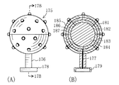
図16は、円錐状の多層構造体を有する表示装置160の実施形態を示している。図16(A)は表示装置160の外観を示しており、図16(B)は表示装置160の中心軸Cに沿った垂直断面図である。この多層構造体165は、表示面170側からそれぞれ順に配置された4つの絶縁性発泡プラスチック層161、162、163および164と、2つの絶縁性発泡プラスチック層161と162の間に挟まれた導電層166と、2つの絶縁性発泡プラスチック層162と163の間に挟まれた別の導電層167と、2つの絶縁性発泡プラスチック層163と164の間に挟まれたさらに別の導電層168とを有する。発泡プラスチック層164の外側表面から中心軸Cまでの距離(厚さ)は一定ではない。多層構造体165には複数の発光ダイオード169a、169bが差込まれている。3つの導電層は直流電源およびスイッチング制御器171に接続されている。
【0038】
図17は、球状の多層構造体を有する表示装置175の実施形態を示している。図17(A)は表示装置175の外観を示しており、図17(B)は表示装置175の球の、中心点を通る垂直面17Bで切った断面図である。その多層構造体は、表示球面側からそれぞれ順に配置された4つの絶縁性発泡プラスチック層181〜184と、絶縁性発泡プラスチック層の間に挟まれた導電層185〜187とを有し、多数の発光素子が差込まれている。この表示装置175は、基台178とその上に球状の多層構造体を支持するロッド176とを有する。ロッド176内には3本の給電線の束177が収容されている。基台178内には直流電源およびスイッチング制御器179が設けられている。その3本の給電線は、直流電源179から多層構造体内のそれぞれの導電層に接続されている。
【0039】
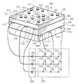
図18は、表示面が複数の領域に分割されている多層構造体を有する表示装置200の実施形態の外観(斜視図)を示している。表示装置200の多層構造体は、第1、第2および第3の絶縁層201、202および203、および第1と第2の導電層206および207からなる多層構造体を具えている。
【0040】
図19は、図18の多層構造体の構成を示すための分解図である。第1の導電層206は、絶縁間隙276および277によって複数の領域311、312および313に分離されており、その領域311、312および313には電極241、242および243がそれぞれ接続されている。第2の導電層207は、絶縁間隙276および277に交差するまたは概ね直交する方向の絶縁間隙278および279によって複数の領域351、352および353に分離されており、その領域351、352および353には電極246、247および248がそれぞれ接続されている。その積層構造体において、第1の導電層206の領域311、312および313と第2の導電層207の領域351、352および353とは、図19から分かるように表示面250から見て互いに部分的にオーバラップしている。電極241、242および243は直流電源装置260の直流電源261、262および263の一方の極性(例えば負)の電極に接続されている。電極246、247および248はスイッチ装置250を介して直流電源装置250の直流電源261、262および263の他方の極性(例えば正)の電極に接続されている。スイッチ装置250はマトリックス状のスイッチ251〜259を有する。図18の上側の多層構造体の表示面250に境界線または絶縁間隙276、277、278および279を投影した場合の位置が破線271、272、273および274によって示されている。このようにして、表示面250は、第1と第2の導電層206および207のそれぞれの互いに分離された複数の領域に対応して、複数の表示領域211、212、213、221、222、223、231、232および233に分割されている。この複数の表示領域によって表示面250の発光ダイオードは9つの表示領域にグループ化されまたは分割される。
【0041】
図18において第1の導電層206に給電するための1つのスイッチ、例えば251をオン状態にすると、表示領域211の発光素子だけが選択されて発光する。さらに、例えばスイッチ251および255をオン状態にすると、表示領域211および222の発光素子が選択されて発光する。
【0042】
図20は図18の複数の表示領域を有する多層構造体200の別の構造を示すための分解図である。第1絶縁層201は、第1の導電層206の絶縁間隙276および277に対応する間隙281および282によって複数の領域311、312および313に分離されている。第3絶縁層203は、第2の導電層207の絶縁間隙278および279に対応する間隙283および284によって複数の部材351、352および353に分離されている。第1の導電層206の絶縁間隙276および277に対応する2つの溝285および286が、第2絶縁層202の上面から内部に向かって延びている。第2の導電層207の絶縁間隙278および279に対応する2つの溝287および288が、第2絶縁層202の下面から内部に向かって延びている。絶縁層のその間隙および溝は、空き空間としてもよく、または絶縁性のゴムまたはビニルのシートによってその空間を埋めてもよい。
【0043】
図20に示した構造体は、積層ボードにその上面から間隙281および282の位置に、表示面側から第2の絶縁層202の内部に達するように切り込みを入れ、それによって間隙281および282と第1の導電層206の間隙276および277と第2の絶縁層202の溝285および286とを形成し、また、積層ボードにその下面から間隙283および284の位置に、底面から第2の絶縁層202の内部に達するように切り込みを入れ、それによって間隙283および284と第2の導電層207の間隙278および279と第2の絶縁層202の溝287および288とを形成して得られる。このようにして、図18および19に示した表示装置200と基本的に同じ表示装置が簡単な方法で作成できる。
【0044】
図21は、図18の複数の表示領域を有する多層構造体200の別の構造を示すための分解図である。この図において、第1の導電層206は、表示領域211〜233に対応して複数の領域371〜379に分離されている。第1の導電層206の複数の領域371〜379には電極381〜389がそれぞれ接続されている。第2の導電層207は電極391に接続されている。電極381〜389はそれぞれ図示されていない個々のスイッチを介して図示されていない直流電源の一方の極性の電極に接続されている。電極391は直流電源の他方の極性の電極に接続されている。この構成によって、個々のスイッチをオン状態にすると、対応する個々の表示領域の発光素子だけが選択されて発光する。
【0045】
本発明による表示装置においては、複数の導電層を用い、それぞれ受電する導電層の位置(深さ)が異なる2つの端子を有する発光素子を用いるので、1つの導電層位置に2つ以上の所定導体ストリップ・パターンを形成しなくても、発光素子の各端子に所定電位を与えることができる。これに対して、プリント基板上に1つ以上の発光素子を配置する場合には、基板上に少なくとも2つの電位を与える導体配線パターンを形成する必要があるであろう。
【0046】
本発明に従う発光素子を有する表示装置には次のような用途がある。(1)アート表示装置。発光素子を有するサインボードは、芸術的表現の媒体としてアート・サインボードに応用できる。また、看板や標識として使用することもできる。さらに、そのアート・サインボードを子供用の玩具として利用することができる。図17に示した表示装置は例えば光る球状装飾品として使用できる。(2)切換え型サインボード。上述したように複数の群の発光ダイオードをスイッチを介して切換えて発光させることによって、複数の情報を切換えて表示することができる。例えば、駐車場の満車を示す「満」と空きスペースの存在を示す「空」をスイッチで切換えて表示することができる。(3)遊戯用の製品。例えば、上述のサインボードをすごろくの駒の形状に加工して使用することができる。(4)大型の地域案内地図や観光案内地図。大型のサインボードの表示面に地図を描き、発光ダイオードを取付けることによって名所旧跡や特定の施設の位置を表示でき、状況の変化に応じてその発光ダイオードの差込み位置を柔軟に追加または変更することができる。(5)建材。壁、天井および扉等の建材として使用すると、意匠性のある建材になる。(6)工芸品。サインボードを薄い円盤状に形成して電池内蔵の棒状の手持ち部を付加すると意匠性のある「光るうちわ」が形成される。その他の工芸品にも応用可能である。
【0047】
以上説明した実施形態は典型例として挙げたに過ぎず、当業者であれば本発明の原理および範囲を逸脱することなく種々の変形を行えることは明らかである。
【図面の簡単な説明】
【図1】図1は、本発明の一実施形態の外観(斜視図)を示している。
【図2】図2は、本発明の表示装置の原理を示す図である。
【図3】図3は、図2のサインボードの線3−3で切った垂直断面図である。
【図4】図4は、導電層の種々の実施例を示している。
【図5】図5は、発光ダイオードの種々の実施例を示している。
【図6】図6は、発光ダイオードの端子を多層ボードに直接突き刺した例を示している。
【図7】図7は、発光ダイオードの各端子の先端部を示している。
【図8】図8(A)は、導電層と給電ケーブルとの接続法を例示している。図8(B)は、導電層と給電ケーブルとの別の接続法を例示している。図8(C)は給電用銅板の変形例を示している。
【図9】図9は、リレー・スイッチを介した電源の接続法を例示している。
【図10】図10は、2つの表示面を有するサインボードにおける同時に点灯する発光ダイオードの配置を示している。
【図11】図11は、2つの表示面を有するサインボードにおける選択的に点灯する発光ダイオードの配置を示している。
【図12】図12は、作動電圧の異なる2種類の発光ダイオードを使用したサインボードを示している。
【図13】図13は、3つの導電層を使用するサインボードにおける種々の発光ダイオードの1対の端子の長さを示している。
【図14】図14は、3つの導電層と2つの表示面とを有するサインボードにおける種々の発光ダイオードを示している。
【図15】図15は、所定パターンのストリップに結線して取付けられ差込み端子数を減少させた複数の発光ダイオードを示している。
【図16】図16(A)は、円錐状の多層構造体を有する表示装置の実施形態の外観(側面図)を示している。図16(B)はこの表示装置の垂直断面図である。
【図17】図17(A)は、球状の多層構造体を有する表示装置の実施形態の外観(側面図)を示している。図17(B)はこの表示装置の垂直断面図である。
【図18】図18は、導電層が複数の領域に分割されている多層構造体を有する表示装置の実施形態の外観(斜視図)を示している。
【図19】図19は、図18の多層構造体の構造を示すための図である。
【図20】図20は、図18の多層構造体200の別の構造を示すための図である。
【図21】図21は、図18の多層構造体200の別の構造を示すための図である。
【符号の説明】
10 多層ボード
11、12、13 発泡プラスチック・ボード
21、22 導電層
31 発光ダイオード
42、43 発光ダイオードの端子
16 直流電源
44 端子の絶縁性被覆[0001]
BACKGROUND OF THE INVENTION
The present invention relates to a display device in which a plurality of light emitting elements are mounted at substantially arbitrary positions on a display surface of a multilayer structure, and a multilayer structure and a light emitting element for such a display device.
[0002]
[Prior art]
A lightning plate having a structure in which a light emitting diode having a short electrode plug and a long electrode plug that insulates a required portion is placed on a board having a plurality of plate-like electrical conductors and a plurality of plate-like insulators is known. .
[0003]
A long electrode having a short electrode and an insulating coating layer on a display plate comprising two conductive thin plates made of rubber, synthetic resin or metal mixed with fine powder of a conductive substance and an insulating thin plate sandwiched between them There has been known a position display device into which a light-emitting diode having a gap is inserted.
[0004]
Light emission having a long contact needle and a short contact needle in which a laminated sheet composed of two or three conductive layers of metal foil or conductive resin and two or three insulating layers of soft synthetic resin is covered with insulation except for the tip. A display device in which a diode is inserted and contacted is known.
[0005]
However, in such a conventional display device, the contact between the terminal (lead frame) of the light emitting diode and the conductive layer is insufficient and unstable, and some of the light emitting diodes have sufficient electrical contact with the terminal. There is a tendency that light cannot be emitted without being obtained, or the contact portion is oxidized with time and power cannot be supplied. Further, in such a conventional display device, it is not possible to select a region of the light emitting element to be turned on.
[0006]
One object of the present invention is to realize a display device in which a light emitting element can be attached at a substantially arbitrary position on the display surface of the display device. Another object of the present invention is to realize a conductive layer that forms a stable conductive contact with a light emitting element terminal inserted in a multilayer structure for a display device. Still another object of the present invention is to realize a display device capable of selecting a region of a light emitting element to be turned on.
[0007]
SUMMARY OF THE INVENTION
In order to solve the above problems, the present inventionAccording to the features of the embodiment,The display device (1)OneThe first, second, and third insulating layers (11, 12, 13) arranged in order from the display surface side, and the first conductivity sandwiched between the first and second insulating layers A multilayer structure (10) having a layer (21) and a second conductive layer (22) sandwiched between second and third insulating layers; attached to the display surface of the multilayer structure 1st and 2nd light emitting element (31; 91,92) and the change-over switch (FIG. 9) connected to DC power supply are provided. The first, second, and third insulating layers are made of a material that can be pierced by a needle-like object to open a hole. First and second conductive layersEach ofIsIncluding a plurality of conductive fabrics laminated, each fabric of the plurality of fabricsCan be pierced with needles to make holesChemical fiber or naturalIncluding fiberHas a metal coating. The first light emitting element has a first conductor terminal having a long polarity and a second conductor terminal having a second polarity. The second light-emitting element has a second long-polarity conductor terminal (42) and a first short-polarity conductor terminal (43). The pair of both conductor terminals is inserted into the multilayer structure from the display surface side. The pair of both conductor terminals of each of the first and second light emitting elements can be inserted into a substantially arbitrary position on the display surface of the multilayer structure. Each long conductor terminal of the first and second light-emitting elements penetrates the first and second insulating layers and the first conductive layer by being inserted into the multilayer structure from the display surface side. In contact with the second conductive layer, and further in contact with the first conductive layer in a portion of the multilayer structure corresponding to the position of the first conductive layer (ie, when inserted into the multilayer structure); In part) it has an insulating coating (44) to insulate it from the first conductive layer.The insulating coating has a tapered or tapered shape.The short conductor terminals of the first and second light emitting elements are inserted into the multilayer structure from the display surface side, thereby penetrating the first insulating layer and contacting the first conductive layer. When the voltage of the first polarity is applied to the first conductive layer and the voltage of the second polarity is applied to the second conductive layer by the changeover switch, the second light emitting element is turned on and the first light emitting element is turned on. When the first polarity voltage is applied to the second conductive layer by the changeover switch and the second polarity voltage is applied to the first conductive layer, the first light emitting element is turned on and the second The light emitting element is turned off.
[0008]
Of the present inventionOf the embodimentAccording to another characteristic, the first, second and third insulating layers are made of insulating foamed plastic. According to yet another feature of the invention, of the first and second conductive layers,One is a first plurality of boundary lines and a second plurality of boundary lines intersecting the first plurality of boundary lines.Minutes into multiple areasSeparationHas been. According to still another feature of the present invention, the long conductor terminal of the light emitting element has an insulating coating on at least a predetermined part of the terminal portion on the light emitting section side corresponding to the length of the short conductor terminal of the light emitting element..
[0009]
【The invention's effect】
According to the configuration of the present invention, the above-described object can be achieved. Further, according to the present invention, the flexibility of the mounting position of the light emitting element in the display device and the stability of the mounting can be obtained, and an image of a stippled form having artistic or design properties can be expressed on the display device. can do.
[0010]
According to a feature of an embodiment of the present invention, the first and second conductive layers comprise a layer comprising a woven or non-woven fabric, the woven or non-woven fabric being in stable electrical contact with the conductor terminals of the light emitting device. Form.
[0011]
DETAILED DESCRIPTION OF THE INVENTION
FIG. 1 shows an appearance (perspective view) of a
[0012]
2 and 3 are diagrams for explaining the principle of the configuration and operation of the display device of the present invention. 3 is a vertical cross-sectional view of the sign board of FIG. 2 taken along line 3-3. 2 and 3, each light-
[0013]
2 and 3, the two
[0014]
Next, the configuration of the insulating
[0015]
In such a foamed plastic board, a needle having a pointed tip, such as a carpet fixing pin (鋲), is pierced into the board to form a
[0016]
Next, the configuration of the
[0017]
FIG. 4A shows an example of the
[0018]
Next, the structure of the light emitting element will be described.
The light-emitting
[0019]
Next, the structure of the terminal of the light emitting diode will be described with reference to FIGS. 2 and 3. One terminal (negative electrode) 43 of the
[0020]
FIG. 5 shows various embodiments of the insulating
[0021]
FIG. 5 (C) shows that the above-mentioned terminal portion is made of an insulating coating with a hollow hollow tube made of an insulating long rigid, semi-rigid or soft plastic, or a rubber tube, for example, an alkali resin tube or a Teflon tube having an outer diameter of about 1 mm. An example of covering and forming is shown. In that case, if a hollow tube of hard plastic resin (eg, fluororesin) is used and the end thereof is cut obliquely and processed into a tapered shape, a terminal is directly pierced into the
[0022]
FIG. 5D shows an example in which the insulating coating is formed by winding an insulating plastic adhesive tape (so-called cellophane tape or vinyl tape) around the terminal portion described above. FIG. 5E shows that two electrode terminals are formed concentrically, that is, one terminal is a needle electrode disposed on the central axis, and the other terminal is a tubular electrode disposed concentrically. An example in which an insulating plastic or an inter-electrode insulating layer is formed by filling an insulating plastic between them is shown. Although not shown, the insulating coating is similar to that shown in FIG. 5 (D), and the above-mentioned terminal portion is coated with enamel or insulating adhesive (eg, based on vinyl chloride / vinyl acetate copolymer using thinner as a solvent). It may be formed by applying a substantially uniform thickness.
[0023]
When the adhesion of the insulating coating to the terminals of the light emitting diode is good, the terminals of the light emitting diode can be directly pierced into the multilayer board as shown in FIG. If the insulation of the insulation coating on the terminal is poor, the insulation coating may be peeled off, turned up, or detached when the terminal is directly pierced into the multilayer board. It is better to form a
[0024]
As shown in FIG. 7, the tip of each terminal of the light-emitting diode is easily sharpened by sharpening the periphery of the tip to make good electrical contact with the conductive layer. It becomes easy to pierce the board.
[0025]
Next, a connection method between the
[0026]
Next, another connection method between the
[0027]
The DC power source may be a battery or a DC power source including a rectifier and a smoothing capacitor connected to the AC power source, preferably via a variable resistor or a selected fixed resistor so that a current of about 20 mA flows through each light emitting diode. Adjust the supply current. Further, when a light-emitting diode with a built-in resistor (for example, a product made by Hewlett Packard having a rated voltage of 5 V) is used, it is not necessary to provide a separate resistor.
[0028]
The conductive layer described above does not need to be formed into a wiring strip pattern, and the above-described light emitting diode can be attached to almost any position on the display surface of the multilayer board without being soldered to the conductive layer. Since it can be removed from that position, it is possible to adjust the mounting position while watching the work on the signboard. Therefore, the work can be completed with a pointillistic sensation in consideration of the artistry or the design. After the arrangement on the display surface of the light emitting diode (more specifically, the effective display surface having the conductive layer below) is finally determined, an adhesive is applied to the bottom surface of the
[0029]
Next, in the embodiment of FIG. 9, as in FIGS. 1 to 3, the negative electrode of the DC power supply is connected to the first
[0030]
Next, another embodiment of the present invention will be described with reference to FIG. In this embodiment, both sides of the sign board are used as display surfaces. On the upper first display surface, as in the first embodiment, the + LS type
[0031]
Next, still another embodiment of the present invention will be described with reference to FIG. In this embodiment, + LS type and + SL type light emitting diodes as shown in FIG. 9 are used for the first and second display surfaces, respectively. When the polarity of the DC power source connected to the two
[0032]
Next, still another embodiment of the present invention will be described with reference to FIG. The sign board of this embodiment uses two types of light emitting diodes having different lengths on the upper display surface, and has four insulating
[0033]
As shown in Table 1 and FIG. 13, there are six types of relationship between the polarity and length of a pair of terminals of a light emitting diode that can be used in the embodiment using the three conductive layers of the present invention. In Table 1, + and-indicate terminal polarities, and S (short), M (intermediate), and L (long) indicate terminal lengths. If two types of light emitting diodes for operating voltages of about 2 V and about 4 V are used for this, a total of 12 types of light emitting diode options are obtained. Further, when four color light emitting diodes are used, 48 types of light emitting diode options can be obtained. FIG. 13 also shows various forms of DC power supplies of about 2V and about 4V.
[Table 1]
FIG. 14 shows how the light emitting diode is used when both sides of the sign board are used as display surfaces and three conductive layers are used.
[0035]
When using a light emitting diode on the display surface of a multi-layer board to represent characters (characters, numbers, etc.) or curves in a predetermined pattern, the correct character or curve shape can be expressed by inserting the light emitting diodes individually into the multi-layer board. As shown in FIG. 15, a plurality of light emitting diodes are inserted into a predetermined pattern, for example, a T-shaped insulative strip (strip), and bonded to the predetermined light emitting diodes. An array pattern may be formed, and the predetermined light emitting diode array pattern may be inserted into the multilayer board. FIG. 15A is a perspective view showing the upper side of a T-shaped insulating
[0036]
In the display device of the above-described embodiment, a multilayer board having a flat (planar) surface is used as the multilayer structure. However, the multilayer structure is not limited to a flat surface, but a spherical shape, It may have a non-planar curved surface such as a cylinder or a cone.
[0037]
FIG. 16 shows an embodiment of a
[0038]
FIG. 17 shows an embodiment of a
[0039]
FIG. 18 shows an appearance (perspective view) of an embodiment of the
[0040]
FIG. 19 is an exploded view showing the configuration of the multilayer structure of FIG. The first
[0041]
In FIG. 18, when one switch for supplying power to the first
[0042]
FIG. 20 is an exploded view showing another structure of the
[0043]
In the structure shown in FIG. 20, the laminated board is cut from the upper surface to the positions of the
[0044]
FIG. 21 is an exploded view showing another structure of the
[0045]
In the display device according to the present invention, a light emitting element using a plurality of conductive layers and having two terminals each having a different position (depth) of the conductive layer to receive power is used. A predetermined potential can be applied to each terminal of the light emitting element without forming a conductor strip pattern. On the other hand, when one or more light emitting elements are arranged on a printed board, it will be necessary to form a conductor wiring pattern that applies at least two potentials on the board.
[0046]
The display device having a light emitting element according to the present invention has the following uses. (1) Art display device. A sign board having a light emitting element can be applied to an art sign board as a medium of artistic expression. It can also be used as a signboard or sign. Furthermore, the art sign board can be used as a toy for children. The display device shown in FIG. 17 can be used as, for example, a glowing spherical ornament. (2) Switching type sign board. As described above, a plurality of pieces of information can be switched and displayed by switching a plurality of groups of light emitting diodes through a switch to emit light. For example, “full” indicating that the parking lot is full and “empty” indicating the presence of an empty space can be switched and displayed by a switch. (3) Products for play. For example, the above-mentioned sign board can be used by processing it into the shape of an amazing piece. (4) Large area guide maps and tourist guide maps. By drawing a map on the display surface of a large signboard and attaching a light emitting diode, you can display the location of historical sites and specific facilities, and flexibly add or change the insertion position of the light emitting diode as the situation changes Can do. (5) Building materials. When used as building materials such as walls, ceilings and doors, it becomes a building material with a design. (6) Crafts. When a sign board is formed into a thin disk shape and a rod-like hand-held portion with a built-in battery is added, a “shining fan” with design is formed. It can be applied to other crafts.
[0047]
The embodiment described above is merely given as a typical example, and it is obvious that those skilled in the art can make various modifications without departing from the principle and scope of the present invention.
[Brief description of the drawings]
FIG. 1 shows an appearance (perspective view) of an embodiment of the present invention.
FIG. 2 is a diagram showing the principle of the display device of the present invention.
FIG. 3 is a vertical cross-sectional view of the sign board of FIG. 2 taken along line 3-3.
FIG. 4 shows various embodiments of conductive layers.
FIG. 5 shows various embodiments of light emitting diodes.
FIG. 6 shows an example in which a terminal of a light emitting diode is directly pierced into a multilayer board.
FIG. 7 shows a tip portion of each terminal of the light emitting diode.
FIG. 8A illustrates a connection method between a conductive layer and a power feeding cable. FIG. 8B illustrates another connection method between the conductive layer and the feeding cable. FIG. 8C shows a modification of the power feeding copper plate.
FIG. 9 illustrates a method for connecting a power supply via a relay switch.
FIG. 10 shows an arrangement of light emitting diodes that are lighted simultaneously on a sign board having two display surfaces.
FIG. 11 shows an arrangement of light-emitting diodes that are selectively lit on a sign board having two display surfaces.
FIG. 12 shows a sign board using two types of light emitting diodes with different operating voltages.
FIG. 13 shows the length of a pair of terminals of various light emitting diodes in a sign board using three conductive layers.
FIG. 14 shows various light emitting diodes in a sign board having three conductive layers and two display surfaces.
FIG. 15 shows a plurality of light emitting diodes connected to a strip having a predetermined pattern and having a reduced number of plug-in terminals.
FIG. 16A shows an appearance (side view) of an embodiment of a display device having a conical multilayer structure. FIG. 16B is a vertical cross-sectional view of this display device.
FIG. 17A shows an appearance (side view) of an embodiment of a display device having a spherical multilayer structure. FIG. 17B is a vertical cross-sectional view of this display device.
FIG. 18 shows an appearance (perspective view) of an embodiment of a display device having a multilayer structure in which a conductive layer is divided into a plurality of regions.
FIG. 19 is a diagram for illustrating the structure of the multilayer structure of FIG. 18;
FIG. 20 is a view for illustrating another structure of the
FIG. 21 is a view for illustrating another structure of the
[Explanation of symbols]
10 Multi-layer board
11, 12, 13 Foamed plastic board
21, 22 Conductive layer
31 Light-emitting diode
42, 43 Light-emitting diode terminals
16 DC power supply
44 Terminal insulation coating
Claims (3)
前記多層構造体の前記1つの表示面に取付けられる第1および第2の発光素子と、
直流電源に接続される切換スイッチと、
を具える表示装置であって、
前記第1と第2と第3の絶縁性層は、針状物によって突き刺して孔を開けることができる素材からなるものであり、前記第1と第2の導電性層の各々は、針状物によって突き刺して孔を開けることができる積層された複数の導電性の布を含み、前記布は化学繊維または天然繊維を含みかつ金属被覆を有し、
前記第1の発光素子は第1の極性の長い導体端子と第2の極性の短い導体端子とを有し、前記第2の発光素子は前記第1の極性の短い導体端子と前記第2の極性の長い導体端子とを有し、前記第1および第2の発光素子の各々の前記両導体端子の対は、前記多層構造体に前記表示面側から差込まれ、前記多層構造体の前記表示面における実質的に任意の位置に差込み可能なものであり、
前記第1および第2の発光素子のそれぞれの長い導体端子は、前記多層構造体に前記表示面側から差込まれることによって前記第1と第2の絶縁性層と前記第1の導電性層とを貫通して前記第2の導電性層に接触し、さらに前記多層構造体における前記第1の導電性層の位置に対応する部分に絶縁被覆を有していて前記第1の導電性層に対して絶縁され、前記絶縁被覆は、前記長い導体端子の先端側が細いテーパ状または先細の形状を有し、
前記第1および第2の発光素子のそれぞれの短い導体端子は、前記多層構造体に前記表示面側から差込まれることによって前記第1の絶縁性層を貫通して前記第1の導電性層に接触し、
前記切換スイッチによって前記第1の極性の電圧が前記第1の導電層に印加され前記第2の極性の電圧が前記第2の導電層に印加されたとき、前記第2の発光素子が点灯し前記第1の発光素子が消灯し、前記切換スイッチによって前記第1の極性の電圧が前記第2の導電層に印加され前記第2の極性の電圧が前記第1の導電層に印加されたとき、前記第1の発光素子が点灯し前記第2の発光素子が消灯するものである、
表示装置。 First, second and third insulating layers disposed in order from one display surface side, a first conductive layer sandwiched between the first and second insulating layers, A multilayer structure having a second conductive layer sandwiched between second and third insulating layers;
First and second light-emitting element mounted on said one display surface of the multilayer structure,
A changeover switch connected to a DC power supply;
A display device comprising:
The first, second, and third insulating layers are made of a material that can be pierced by a needle-like material, and each of the first and second conductive layers is needle-like. includes a plurality of conductive fabric are laminated may be a hole pierce by things, the fabric has a free Mikatsu metallization chemical fibers or natural fibers,
The first light emitting element has a first conductor terminal with a long polarity and a second conductor terminal with a short second polarity, and the second light emitting element has a conductor terminal with a short first polarity and the second conductor terminal. A pair of conductor terminals of each of the first and second light-emitting elements is inserted into the multilayer structure from the display surface side, and the multilayer structure has the conductor terminal having a long polarity. It can be inserted into virtually any position on the display surface,
The long conductor terminals of the first and second light emitting elements are inserted into the multilayer structure from the display surface side, whereby the first and second insulating layers and the first conductive layer are inserted. And the first conductive layer has an insulating coating on a portion corresponding to the position of the first conductive layer in the multilayer structure. The insulating coating has a tapered shape or a tapered shape on the distal end side of the long conductor terminal,
The short conductive terminals of the first and second light emitting elements are inserted into the multilayer structure from the display surface side so as to penetrate the first insulating layer and to form the first conductive layer. In contact with
When the voltage having the first polarity is applied to the first conductive layer and the voltage having the second polarity is applied to the second conductive layer by the changeover switch, the second light emitting element is turned on. When the first light emitting element is extinguished, the voltage of the first polarity is applied to the second conductive layer by the changeover switch, and the voltage of the second polarity is applied to the first conductive layer The first light emitting element is turned on and the second light emitting element is turned off.
Display device.
前記多層構造体の前記1つの表示面に取付けられる第1および第2の発光半導体素子と、
直流電源に接続される切換スイッチと、
を具える表示装置であって、
前記第1と第2と第3の絶縁性発泡プラスチック層は針状物によって突き刺して孔を開けることができるものであり、前記第1と第2の導電性層の各々は、針状物によって突き刺して孔を開けることができる積層された複数の導電性の布を含み、前記布は化学繊維または天然繊維を含みかつ金属被覆を有し、
前記第1および第2の発光半導体素子の各々は第1と第2の導体端子を有し、この両導体端子の対は前記多層構造体に前記表示面側から差込まれ、前記両導体端子の対は前記多層構造体の表示面における実質的に任意の位置に差込み可能なものであり、
前記第1の導体端子は前記多層構造体に前記表示面側から差込まれることによって前記第1と第2の絶縁性発泡プラスチック層と前記第1の導電性層とを貫通して前記第2の導電性層に接触し、前記第1の導体端子は前記多層構造体における前記第1の導電性層の位置に対応する部分に絶縁被覆を有していて前記第1の導電性層に対して絶縁され、前記絶縁被覆は、前記第1の導体端子の先端側が細いテーパ状または先細の形状を有し、
前記第2の導体端子は前記多層構造体に前記表示面側から差込まれることによって前記第1の絶縁性発泡プラスチック層を貫通して前記第1の導電性層に接触し、
前記切換スイッチによって第1の極性の電圧が前記第1の導電層に印加され第2の極性の電圧が前記第2の導電層に印加されたとき、前記第2の発光素子が点灯し前記第1の発光素子が消灯し、前記切換スイッチによって前記第1の極性の電圧が前記第2の導電層に印加され前記第2の極性の電圧が前記第1の導電層に印加されたとき、前記第1の発光素子が点灯し前記第2の発光素子が消灯するものである、
表示装置。 First, second, and third insulating foamed plastic layers disposed in order from one display surface side, and a first conductive sandwiched between the first and second insulating foamed plastic layers A multilayer structure having a layer and a second conductive layer sandwiched between the second and third insulating foam plastic layers;
First and second light-emitting semiconductor element mounted on said one display surface of the multilayer structure,
A changeover switch connected to a DC power supply;
A display device comprising:
The first, second and third insulating foamed plastic layers can be pierced with a needle-like material to form a hole, and each of the first and second conductive layers is made of a needle-like material. piercing and includes a plurality of conductive fabric are laminated may be a hole, wherein the fabric has a free Mikatsu metallization chemical fibers or natural fibers,
Each of the first and second light emitting semiconductor elements has first and second conductor terminals, and a pair of both conductor terminals is inserted into the multilayer structure from the display surface side. The pair of can be inserted into substantially any position on the display surface of the multilayer structure,
The first conductor terminal is inserted into the multilayer structure from the display surface side, thereby penetrating the first and second insulating foamed plastic layers and the first conductive layer, and the second conductive terminal. The first conductor terminal has an insulating coating in a portion corresponding to the position of the first conductive layer in the multilayer structure, and the first conductive terminal is in contact with the first conductive layer. The insulating coating has a tapered shape or a tapered shape on the tip side of the first conductor terminal;
The second conductor terminal is inserted into the multilayer structure from the display surface side, penetrates the first insulating foam plastic layer, and contacts the first conductive layer,
When a voltage having a first polarity is applied to the first conductive layer and a voltage having a second polarity is applied to the second conductive layer by the changeover switch, the second light emitting element is turned on, and the first When the light emitting element of 1 is turned off, the voltage of the first polarity is applied to the second conductive layer by the changeover switch, and the voltage of the second polarity is applied to the first conductive layer, the The first light emitting element is turned on and the second light emitting element is turned off.
Display device.
前記多層構造体の前記表示面に取付けられる複数の発光素子と、
を具える表示装置であって、
前記第1と第2と第3の絶縁性層は、針状物によって突き刺して孔を開けることができる素材からなるものであり、前記第1と第2の導電性層の各々は、針状物によって突き刺して孔を開けることができる積層された複数の導電性の布を含み、前記布は化学繊維または天然繊維を含みかつ金属被覆を有し、
前記第1と第2の導電性層の一方が、第1の複数の境界線と、前記第1の複数の境界線と交差する第2の複数の境界線とで複数の領域に分離されており、
前記複数の発光素子の各々は長い導体端子と短い導体端子とを有し、この両導体端子の対は前記多層構造体に差込まれ、前記両導体端子の対は前記多層構造体の前記表示面における実質的に任意の位置に差込み可能なものであり、
前記長い導体端子は前記多層構造体に差込まれることによって前記第1と第2の絶縁性層と前記第1の導電性層とを貫通して前記第2の導電性層に接触し、前記長い導体端子は前記多層構造体における前記第1の導電性層の位置に対応する部分に絶縁被覆を有していて前記第1の導電性層に対して絶縁され、前記絶縁被覆は、前記長い導体端子の先端側が細いテーパ状または先細の形状を有し、
前記短い導体端子は前記多層構造体に差込まれることによって前記第1の絶縁性層を貫通して前記第1の導電性層に接触するものである、
表示装置。First, second and third insulating layers disposed in order from the display surface side, a first conductive layer sandwiched between the first and second insulating layers, and the second A multilayer structure having a second conductive layer sandwiched between and a third insulating layer;
A plurality of light emitting elements attached to the display surface of the multilayer structure
A display device comprising:
It said first and second and the third insulating layer is made of a material capable of drilling holes pierced by needles, each of said first and second conductive layers are needle A plurality of laminated conductive fabrics that can be pierced and pierced by an object, said fabrics comprising chemical fibers or natural fibers and having a metal coating ;
One of said first and second conductive layers, a first plurality of boundary lines, min is separated into a plurality of regions in the second plurality of boundary lines intersecting the first plurality of boundary lines And
Each of the plurality of light emitting elements has a long conductor terminal and a short conductor terminal, and a pair of both conductor terminals is inserted into the multilayer structure, and the pair of both conductor terminals is the display of the multilayer structure. Can be inserted into virtually any position on the surface,
The long conductor terminal is inserted into the multilayer structure so as to pass through the first and second insulating layers and the first conductive layer to contact the second conductive layer, and long conductor terminal is insulated with respect to the multi-layer structure wherein the first conductive layer have an insulating coating to a portion corresponding to the position of the first conductive layer in body, wherein the insulating coating, the longer The tip side of the conductor terminal has a thin tapered shape or a tapered shape,
The short conductor terminal is to be you contact with the first conductive layer through said first insulating layer by being plugged into the multilayer structure,
Display device.
Priority Applications (1)
| Application Number | Priority Date | Filing Date | Title |
|---|---|---|---|
| JP2000378592A JP4647091B2 (en) | 1999-12-13 | 2000-12-13 | Display device, multilayer structure for display device, and light emitting diode for display device |
Applications Claiming Priority (5)
| Application Number | Priority Date | Filing Date | Title |
|---|---|---|---|
| JP35319399 | 1999-12-13 | ||
| JP2000111176 | 2000-04-12 | ||
| JP2000-111176 | 2000-04-12 | ||
| JP11-353193 | 2000-04-12 | ||
| JP2000378592A JP4647091B2 (en) | 1999-12-13 | 2000-12-13 | Display device, multilayer structure for display device, and light emitting diode for display device |
Publications (3)
| Publication Number | Publication Date |
|---|---|
| JP2001356722A JP2001356722A (en) | 2001-12-26 |
| JP2001356722A5 JP2001356722A5 (en) | 2008-03-13 |
| JP4647091B2 true JP4647091B2 (en) | 2011-03-09 |
Family
ID=27341443
Family Applications (1)
| Application Number | Title | Priority Date | Filing Date |
|---|---|---|---|
| JP2000378592A Expired - Lifetime JP4647091B2 (en) | 1999-12-13 | 2000-12-13 | Display device, multilayer structure for display device, and light emitting diode for display device |
Country Status (1)
| Country | Link |
|---|---|
| JP (1) | JP4647091B2 (en) |
Families Citing this family (5)
| Publication number | Priority date | Publication date | Assignee | Title |
|---|---|---|---|---|
| JP2007109679A (en) * | 2004-01-14 | 2007-04-26 | Techno Giken Kk | Plug-in fixing type light emitting device |
| EP2018683A1 (en) * | 2006-05-09 | 2009-01-28 | Philips Intellectual Property & Standards GmbH | Conducting wallpaper |
| JP4981391B2 (en) * | 2006-09-20 | 2012-07-18 | 株式会社村上開明堂 | Wiring structure |
| KR101096665B1 (en) * | 2010-06-24 | 2011-12-21 | 광성기업 주식회사 | Traffic safety board having led module using conductive plate |
| JP5771771B2 (en) * | 2010-10-25 | 2015-09-02 | パナソニックIpマネジメント株式会社 | Lighting apparatus and lighting apparatus using the same |
Citations (2)
| Publication number | Priority date | Publication date | Assignee | Title |
|---|---|---|---|---|
| JPS5229197A (en) * | 1975-09-01 | 1977-03-04 | Akira Fujita | Display unit |
| JPH11305699A (en) * | 1998-04-24 | 1999-11-05 | Otani National Denki Kk | Substrate and electric display device using the substrate |
-
2000
- 2000-12-13 JP JP2000378592A patent/JP4647091B2/en not_active Expired - Lifetime
Patent Citations (2)
| Publication number | Priority date | Publication date | Assignee | Title |
|---|---|---|---|---|
| JPS5229197A (en) * | 1975-09-01 | 1977-03-04 | Akira Fujita | Display unit |
| JPH11305699A (en) * | 1998-04-24 | 1999-11-05 | Otani National Denki Kk | Substrate and electric display device using the substrate |
Also Published As
| Publication number | Publication date |
|---|---|
| JP2001356722A (en) | 2001-12-26 |
Similar Documents
| Publication | Publication Date | Title |
|---|---|---|
| US6657381B1 (en) | Display device having a multi-layered structure with light-emitting devices mounted thereon | |
| US5010463A (en) | Electrified bulletin board with illuminable push-pin | |
| JP5253384B2 (en) | Conductive wallpaper | |
| US7291795B2 (en) | Flexible printed circuits with many tiny holes | |
| JPH1021707A (en) | Long light emitting device | |
| JP6523179B2 (en) | Light emitting unit, light emitting device, and method of manufacturing light emitting unit | |
| JP4647091B2 (en) | Display device, multilayer structure for display device, and light emitting diode for display device | |
| US20040041516A1 (en) | Electroluminescence light emitting display system | |
| US20080298033A1 (en) | Power supply platform and electronic component | |
| JP2008103317A (en) | Light-emitting diode lighting device and power supply device used for this lighting device | |
| JP2006210336A (en) | Lighting device of light-emitting diode | |
| US9297523B2 (en) | LED stickers | |
| JP2003197379A (en) | Conductive material holding sheet and el light emitting device using it | |
| JPH11305699A (en) | Substrate and electric display device using the substrate | |
| US20050226995A1 (en) | Flexible printed circuits with many tiny holes | |
| JPH0619345Y2 (en) | Electrostatic adsorption sheet | |
| CN108575043B (en) | Hand-made circuit board | |
| US20040104671A1 (en) | Electroluminescence light emitting device and method for manufacturing the same | |
| JPH10288969A (en) | Light emitting display device | |
| KR200328232Y1 (en) | Light emitting decoration apparatus | |
| JP2000298443A (en) | Electric illumination panel using electroluminescence light emitting member | |
| KR20070093769A (en) | Free sticking pannel, belt, wire, free sticking led, free sticking led module and sign board | |
| JP2002329584A (en) | El luminescent device | |
| JP3166337U (en) | Electronic circuit materials | |
| JP2001100672A (en) | Conductive laminate and display device using the same |
Legal Events
| Date | Code | Title | Description |
|---|---|---|---|
| A521 | Written amendment |
Free format text: JAPANESE INTERMEDIATE CODE: A523 Effective date: 20071205 |
|
| A621 | Written request for application examination |
Free format text: JAPANESE INTERMEDIATE CODE: A621 Effective date: 20071205 |
|
| RD02 | Notification of acceptance of power of attorney |
Free format text: JAPANESE INTERMEDIATE CODE: A7422 Effective date: 20071221 |
|
| A521 | Written amendment |
Free format text: JAPANESE INTERMEDIATE CODE: A821 Effective date: 20071221 |
|
| A977 | Report on retrieval |
Free format text: JAPANESE INTERMEDIATE CODE: A971007 Effective date: 20100820 |
|
| A131 | Notification of reasons for refusal |
Free format text: JAPANESE INTERMEDIATE CODE: A131 Effective date: 20100831 |
|
| A521 | Written amendment |
Free format text: JAPANESE INTERMEDIATE CODE: A523 Effective date: 20101101 |
|
| TRDD | Decision of grant or rejection written | ||
| A01 | Written decision to grant a patent or to grant a registration (utility model) |
Free format text: JAPANESE INTERMEDIATE CODE: A01 Effective date: 20101124 |
|
| A01 | Written decision to grant a patent or to grant a registration (utility model) |
Free format text: JAPANESE INTERMEDIATE CODE: A01 |
|
| A61 | First payment of annual fees (during grant procedure) |
Free format text: JAPANESE INTERMEDIATE CODE: A61 Effective date: 20101208 |
|
| FPAY | Renewal fee payment (event date is renewal date of database) |
Free format text: PAYMENT UNTIL: 20131217 Year of fee payment: 3 |
|
| R150 | Certificate of patent or registration of utility model |
Ref document number: 4647091 Country of ref document: JP Free format text: JAPANESE INTERMEDIATE CODE: R150 Free format text: JAPANESE INTERMEDIATE CODE: R150 |
|
| R250 | Receipt of annual fees |
Free format text: JAPANESE INTERMEDIATE CODE: R250 |
|
| R250 | Receipt of annual fees |
Free format text: JAPANESE INTERMEDIATE CODE: R250 |
|
| R250 | Receipt of annual fees |
Free format text: JAPANESE INTERMEDIATE CODE: R250 |
|
| R250 | Receipt of annual fees |
Free format text: JAPANESE INTERMEDIATE CODE: R250 |
|
| EXPY | Cancellation because of completion of term |