JP4640264B2 - Planar light source device and display device assembly - Google Patents
Planar light source device and display device assembly Download PDFInfo
- Publication number
- JP4640264B2 JP4640264B2 JP2006154982A JP2006154982A JP4640264B2 JP 4640264 B2 JP4640264 B2 JP 4640264B2 JP 2006154982 A JP2006154982 A JP 2006154982A JP 2006154982 A JP2006154982 A JP 2006154982A JP 4640264 B2 JP4640264 B2 JP 4640264B2
- Authority
- JP
- Japan
- Prior art keywords
- light source
- planar light
- support wall
- liquid crystal
- display device
- Prior art date
- Legal status (The legal status is an assumption and is not a legal conclusion. Google has not performed a legal analysis and makes no representation as to the accuracy of the status listed.)
- Active
Links
- 239000004973 liquid crystal related substance Substances 0.000 claims description 98
- 238000009792 diffusion process Methods 0.000 claims description 63
- 239000011159 matrix material Substances 0.000 claims description 24
- 239000000463 material Substances 0.000 claims description 20
- 230000005540 biological transmission Effects 0.000 claims description 10
- 238000002834 transmittance Methods 0.000 description 31
- 239000010408 film Substances 0.000 description 30
- 239000000758 substrate Substances 0.000 description 25
- 238000000034 method Methods 0.000 description 15
- 238000003860 storage Methods 0.000 description 14
- 238000010586 diagram Methods 0.000 description 11
- 230000003287 optical effect Effects 0.000 description 10
- 238000012937 correction Methods 0.000 description 9
- 230000006870 function Effects 0.000 description 7
- BQCADISMDOOEFD-UHFFFAOYSA-N Silver Chemical compound [Ag] BQCADISMDOOEFD-UHFFFAOYSA-N 0.000 description 6
- 239000000428 dust Substances 0.000 description 6
- 229910052709 silver Inorganic materials 0.000 description 6
- 239000004332 silver Substances 0.000 description 6
- 239000000853 adhesive Substances 0.000 description 5
- 230000001070 adhesive effect Effects 0.000 description 5
- 238000006243 chemical reaction Methods 0.000 description 5
- 239000011521 glass Substances 0.000 description 5
- 238000004519 manufacturing process Methods 0.000 description 5
- 210000002858 crystal cell Anatomy 0.000 description 4
- 230000003247 decreasing effect Effects 0.000 description 4
- 230000014509 gene expression Effects 0.000 description 4
- 239000004033 plastic Substances 0.000 description 4
- 229920003023 plastic Polymers 0.000 description 4
- 230000010287 polarization Effects 0.000 description 4
- 229920003229 poly(methyl methacrylate) Polymers 0.000 description 4
- 229920005668 polycarbonate resin Polymers 0.000 description 4
- 239000004431 polycarbonate resin Substances 0.000 description 4
- 239000004926 polymethyl methacrylate Substances 0.000 description 4
- 230000008569 process Effects 0.000 description 4
- 239000004065 semiconductor Substances 0.000 description 4
- 239000004925 Acrylic resin Substances 0.000 description 3
- 229920000178 Acrylic resin Polymers 0.000 description 3
- 238000005253 cladding Methods 0.000 description 3
- 150000001875 compounds Chemical class 0.000 description 3
- 238000000605 extraction Methods 0.000 description 3
- 238000005286 illumination Methods 0.000 description 3
- 238000012986 modification Methods 0.000 description 3
- 230000004048 modification Effects 0.000 description 3
- 239000000843 powder Substances 0.000 description 3
- 125000006850 spacer group Chemical group 0.000 description 3
- XUIMIQQOPSSXEZ-UHFFFAOYSA-N Silicon Chemical compound [Si] XUIMIQQOPSSXEZ-UHFFFAOYSA-N 0.000 description 2
- 230000008859 change Effects 0.000 description 2
- 238000005401 electroluminescence Methods 0.000 description 2
- 239000003822 epoxy resin Substances 0.000 description 2
- 229920000647 polyepoxide Polymers 0.000 description 2
- 239000011347 resin Substances 0.000 description 2
- 229920005989 resin Polymers 0.000 description 2
- 229910052710 silicon Inorganic materials 0.000 description 2
- 239000010703 silicon Substances 0.000 description 2
- 239000010409 thin film Substances 0.000 description 2
- OAICVXFJPJFONN-UHFFFAOYSA-N Phosphorus Chemical compound [P] OAICVXFJPJFONN-UHFFFAOYSA-N 0.000 description 1
- 239000004698 Polyethylene Substances 0.000 description 1
- 229910045601 alloy Inorganic materials 0.000 description 1
- 239000000956 alloy Substances 0.000 description 1
- 239000003086 colorant Substances 0.000 description 1
- 238000001514 detection method Methods 0.000 description 1
- 230000008713 feedback mechanism Effects 0.000 description 1
- 230000007274 generation of a signal involved in cell-cell signaling Effects 0.000 description 1
- 238000005259 measurement Methods 0.000 description 1
- 229910052751 metal Inorganic materials 0.000 description 1
- 239000002184 metal Substances 0.000 description 1
- 238000012544 monitoring process Methods 0.000 description 1
- 229910021421 monocrystalline silicon Inorganic materials 0.000 description 1
- 239000002245 particle Substances 0.000 description 1
- 230000002093 peripheral effect Effects 0.000 description 1
- 238000007747 plating Methods 0.000 description 1
- 229920001230 polyarylate Polymers 0.000 description 1
- -1 polyethylene Polymers 0.000 description 1
- 229920000573 polyethylene Polymers 0.000 description 1
- 238000012545 processing Methods 0.000 description 1
- 239000004576 sand Substances 0.000 description 1
- 238000005488 sandblasting Methods 0.000 description 1
- 239000003566 sealing material Substances 0.000 description 1
- 230000001360 synchronised effect Effects 0.000 description 1
- KKEYFWRCBNTPAC-UHFFFAOYSA-L terephthalate(2-) Chemical compound [O-]C(=O)C1=CC=C(C([O-])=O)C=C1 KKEYFWRCBNTPAC-UHFFFAOYSA-L 0.000 description 1
- 238000010998 test method Methods 0.000 description 1
Images


Classifications
-
- G—PHYSICS
- G09—EDUCATION; CRYPTOGRAPHY; DISPLAY; ADVERTISING; SEALS
- G09G—ARRANGEMENTS OR CIRCUITS FOR CONTROL OF INDICATING DEVICES USING STATIC MEANS TO PRESENT VARIABLE INFORMATION
- G09G3/00—Control arrangements or circuits, of interest only in connection with visual indicators other than cathode-ray tubes
- G09G3/20—Control arrangements or circuits, of interest only in connection with visual indicators other than cathode-ray tubes for presentation of an assembly of a number of characters, e.g. a page, by composing the assembly by combination of individual elements arranged in a matrix no fixed position being assigned to or needed to be assigned to the individual characters or partial characters
- G09G3/34—Control arrangements or circuits, of interest only in connection with visual indicators other than cathode-ray tubes for presentation of an assembly of a number of characters, e.g. a page, by composing the assembly by combination of individual elements arranged in a matrix no fixed position being assigned to or needed to be assigned to the individual characters or partial characters by control of light from an independent source
- G09G3/3406—Control of illumination source
- G09G3/342—Control of illumination source using several illumination sources separately controlled corresponding to different display panel areas, e.g. along one dimension such as lines
- G09G3/3426—Control of illumination source using several illumination sources separately controlled corresponding to different display panel areas, e.g. along one dimension such as lines the different display panel areas being distributed in two dimensions, e.g. matrix
-
- G—PHYSICS
- G02—OPTICS
- G02F—OPTICAL DEVICES OR ARRANGEMENTS FOR THE CONTROL OF LIGHT BY MODIFICATION OF THE OPTICAL PROPERTIES OF THE MEDIA OF THE ELEMENTS INVOLVED THEREIN; NON-LINEAR OPTICS; FREQUENCY-CHANGING OF LIGHT; OPTICAL LOGIC ELEMENTS; OPTICAL ANALOGUE/DIGITAL CONVERTERS
- G02F1/00—Devices or arrangements for the control of the intensity, colour, phase, polarisation or direction of light arriving from an independent light source, e.g. switching, gating or modulating; Non-linear optics
- G02F1/01—Devices or arrangements for the control of the intensity, colour, phase, polarisation or direction of light arriving from an independent light source, e.g. switching, gating or modulating; Non-linear optics for the control of the intensity, phase, polarisation or colour
- G02F1/13—Devices or arrangements for the control of the intensity, colour, phase, polarisation or direction of light arriving from an independent light source, e.g. switching, gating or modulating; Non-linear optics for the control of the intensity, phase, polarisation or colour based on liquid crystals, e.g. single liquid crystal display cells
- G02F1/133—Constructional arrangements; Operation of liquid crystal cells; Circuit arrangements
- G02F1/1333—Constructional arrangements; Manufacturing methods
- G02F1/1335—Structural association of cells with optical devices, e.g. polarisers or reflectors
- G02F1/1336—Illuminating devices
- G02F1/133602—Direct backlight
- G02F1/133611—Direct backlight including means for improving the brightness uniformity
-
- G—PHYSICS
- G09—EDUCATION; CRYPTOGRAPHY; DISPLAY; ADVERTISING; SEALS
- G09G—ARRANGEMENTS OR CIRCUITS FOR CONTROL OF INDICATING DEVICES USING STATIC MEANS TO PRESENT VARIABLE INFORMATION
- G09G3/00—Control arrangements or circuits, of interest only in connection with visual indicators other than cathode-ray tubes
- G09G3/20—Control arrangements or circuits, of interest only in connection with visual indicators other than cathode-ray tubes for presentation of an assembly of a number of characters, e.g. a page, by composing the assembly by combination of individual elements arranged in a matrix no fixed position being assigned to or needed to be assigned to the individual characters or partial characters
- G09G3/34—Control arrangements or circuits, of interest only in connection with visual indicators other than cathode-ray tubes for presentation of an assembly of a number of characters, e.g. a page, by composing the assembly by combination of individual elements arranged in a matrix no fixed position being assigned to or needed to be assigned to the individual characters or partial characters by control of light from an independent source
- G09G3/3406—Control of illumination source
- G09G3/3413—Details of control of colour illumination sources
-
- G—PHYSICS
- G02—OPTICS
- G02F—OPTICAL DEVICES OR ARRANGEMENTS FOR THE CONTROL OF LIGHT BY MODIFICATION OF THE OPTICAL PROPERTIES OF THE MEDIA OF THE ELEMENTS INVOLVED THEREIN; NON-LINEAR OPTICS; FREQUENCY-CHANGING OF LIGHT; OPTICAL LOGIC ELEMENTS; OPTICAL ANALOGUE/DIGITAL CONVERTERS
- G02F1/00—Devices or arrangements for the control of the intensity, colour, phase, polarisation or direction of light arriving from an independent light source, e.g. switching, gating or modulating; Non-linear optics
- G02F1/01—Devices or arrangements for the control of the intensity, colour, phase, polarisation or direction of light arriving from an independent light source, e.g. switching, gating or modulating; Non-linear optics for the control of the intensity, phase, polarisation or colour
- G02F1/13—Devices or arrangements for the control of the intensity, colour, phase, polarisation or direction of light arriving from an independent light source, e.g. switching, gating or modulating; Non-linear optics for the control of the intensity, phase, polarisation or colour based on liquid crystals, e.g. single liquid crystal display cells
- G02F1/133—Constructional arrangements; Operation of liquid crystal cells; Circuit arrangements
- G02F1/1333—Constructional arrangements; Manufacturing methods
- G02F1/1335—Structural association of cells with optical devices, e.g. polarisers or reflectors
- G02F1/1336—Illuminating devices
- G02F1/133602—Direct backlight
- G02F1/133603—Direct backlight with LEDs
-
- G—PHYSICS
- G02—OPTICS
- G02F—OPTICAL DEVICES OR ARRANGEMENTS FOR THE CONTROL OF LIGHT BY MODIFICATION OF THE OPTICAL PROPERTIES OF THE MEDIA OF THE ELEMENTS INVOLVED THEREIN; NON-LINEAR OPTICS; FREQUENCY-CHANGING OF LIGHT; OPTICAL LOGIC ELEMENTS; OPTICAL ANALOGUE/DIGITAL CONVERTERS
- G02F1/00—Devices or arrangements for the control of the intensity, colour, phase, polarisation or direction of light arriving from an independent light source, e.g. switching, gating or modulating; Non-linear optics
- G02F1/01—Devices or arrangements for the control of the intensity, colour, phase, polarisation or direction of light arriving from an independent light source, e.g. switching, gating or modulating; Non-linear optics for the control of the intensity, phase, polarisation or colour
- G02F1/13—Devices or arrangements for the control of the intensity, colour, phase, polarisation or direction of light arriving from an independent light source, e.g. switching, gating or modulating; Non-linear optics for the control of the intensity, phase, polarisation or colour based on liquid crystals, e.g. single liquid crystal display cells
- G02F1/133—Constructional arrangements; Operation of liquid crystal cells; Circuit arrangements
- G02F1/1333—Constructional arrangements; Manufacturing methods
- G02F1/1335—Structural association of cells with optical devices, e.g. polarisers or reflectors
- G02F1/1336—Illuminating devices
- G02F1/133602—Direct backlight
- G02F1/133609—Direct backlight including means for improving the color mixing, e.g. white
-
- G—PHYSICS
- G02—OPTICS
- G02F—OPTICAL DEVICES OR ARRANGEMENTS FOR THE CONTROL OF LIGHT BY MODIFICATION OF THE OPTICAL PROPERTIES OF THE MEDIA OF THE ELEMENTS INVOLVED THEREIN; NON-LINEAR OPTICS; FREQUENCY-CHANGING OF LIGHT; OPTICAL LOGIC ELEMENTS; OPTICAL ANALOGUE/DIGITAL CONVERTERS
- G02F2201/00—Constructional arrangements not provided for in groups G02F1/00 - G02F7/00
- G02F2201/58—Arrangements comprising a monitoring photodetector
-
- G—PHYSICS
- G09—EDUCATION; CRYPTOGRAPHY; DISPLAY; ADVERTISING; SEALS
- G09G—ARRANGEMENTS OR CIRCUITS FOR CONTROL OF INDICATING DEVICES USING STATIC MEANS TO PRESENT VARIABLE INFORMATION
- G09G2320/00—Control of display operating conditions
- G09G2320/02—Improving the quality of display appearance
- G09G2320/0233—Improving the luminance or brightness uniformity across the screen
-
- G—PHYSICS
- G09—EDUCATION; CRYPTOGRAPHY; DISPLAY; ADVERTISING; SEALS
- G09G—ARRANGEMENTS OR CIRCUITS FOR CONTROL OF INDICATING DEVICES USING STATIC MEANS TO PRESENT VARIABLE INFORMATION
- G09G2320/00—Control of display operating conditions
- G09G2320/02—Improving the quality of display appearance
- G09G2320/0242—Compensation of deficiencies in the appearance of colours
-
- G—PHYSICS
- G09—EDUCATION; CRYPTOGRAPHY; DISPLAY; ADVERTISING; SEALS
- G09G—ARRANGEMENTS OR CIRCUITS FOR CONTROL OF INDICATING DEVICES USING STATIC MEANS TO PRESENT VARIABLE INFORMATION
- G09G2320/00—Control of display operating conditions
- G09G2320/02—Improving the quality of display appearance
- G09G2320/029—Improving the quality of display appearance by monitoring one or more pixels in the display panel, e.g. by monitoring a fixed reference pixel
-
- G—PHYSICS
- G09—EDUCATION; CRYPTOGRAPHY; DISPLAY; ADVERTISING; SEALS
- G09G—ARRANGEMENTS OR CIRCUITS FOR CONTROL OF INDICATING DEVICES USING STATIC MEANS TO PRESENT VARIABLE INFORMATION
- G09G2320/00—Control of display operating conditions
- G09G2320/04—Maintaining the quality of display appearance
- G09G2320/041—Temperature compensation
-
- G—PHYSICS
- G09—EDUCATION; CRYPTOGRAPHY; DISPLAY; ADVERTISING; SEALS
- G09G—ARRANGEMENTS OR CIRCUITS FOR CONTROL OF INDICATING DEVICES USING STATIC MEANS TO PRESENT VARIABLE INFORMATION
- G09G2320/00—Control of display operating conditions
- G09G2320/06—Adjustment of display parameters
- G09G2320/0626—Adjustment of display parameters for control of overall brightness
- G09G2320/064—Adjustment of display parameters for control of overall brightness by time modulation of the brightness of the illumination source
-
- G—PHYSICS
- G09—EDUCATION; CRYPTOGRAPHY; DISPLAY; ADVERTISING; SEALS
- G09G—ARRANGEMENTS OR CIRCUITS FOR CONTROL OF INDICATING DEVICES USING STATIC MEANS TO PRESENT VARIABLE INFORMATION
- G09G2360/00—Aspects of the architecture of display systems
- G09G2360/14—Detecting light within display terminals, e.g. using a single or a plurality of photosensors
- G09G2360/145—Detecting light within display terminals, e.g. using a single or a plurality of photosensors the light originating from the display screen
-
- G—PHYSICS
- G09—EDUCATION; CRYPTOGRAPHY; DISPLAY; ADVERTISING; SEALS
- G09G—ARRANGEMENTS OR CIRCUITS FOR CONTROL OF INDICATING DEVICES USING STATIC MEANS TO PRESENT VARIABLE INFORMATION
- G09G2360/00—Aspects of the architecture of display systems
- G09G2360/16—Calculation or use of calculated indices related to luminance levels in display data
Description
本発明は、面状光源装置及び表示装置組立体に関する。 The present invention relates to a planar light source device and a display device assembly .
液晶表示装置にあっては、液晶材料それ自体は発光しない。従って、例えば、液晶表示装置の表示領域を照射する直下型の面状光源装置(バックライト)を、複数の画素から構成された表示領域の背面に配置する(例えば、文献1:日経エレクトロニクス 2004年12月20日第889号の第123〜130ページ を参照)。尚、カラー液晶表示装置において、1画素は、例えば、赤色発光副画素、緑色発光副画素及び青色発光副画素の3つの副画素から構成されている。そして、各画素あるいは各副画素を構成する液晶セルを、一種の光シャッター(ライト・バルブ)として動作させることによって、即ち、各画素あるいは各副画素の光透過率(開口率)を制御し、面状光源装置から出射された照明光(例えば、白色光)の光透過率を制御することで、画像を表示している。 In the liquid crystal display device, the liquid crystal material itself does not emit light. Therefore, for example, a direct-type planar light source device (backlight) that irradiates the display area of a liquid crystal display device is disposed on the back of the display area composed of a plurality of pixels (for example, Document 1: Nikkei Electronics 2004). December 20th 889, pages 123-130). In the color liquid crystal display device, one pixel includes, for example, three sub-pixels of a red light-emitting sub pixel, a green light-emitting sub pixel, and a blue light-emitting sub pixel. Then, by operating the liquid crystal cell constituting each pixel or each sub-pixel as a kind of light shutter (light valve), that is, controlling the light transmittance (aperture ratio) of each pixel or each sub-pixel, An image is displayed by controlling the light transmittance of illumination light (for example, white light) emitted from the planar light source device.
面状光源装置(バックライト)は、筐体を備え、筐体内に配設された複数の光源、及び、筐体の上部に取り付けられた拡散板から構成されている。光源として、発光ダイオード(LED)や冷陰極線型の蛍光ランプが使用される。また、一般に、拡散板はプラスチックから作製されており、液晶表示装置の大きさにより異なるが、板厚は2mm程度であり、拡散板を水平に保持したとき、それ自体で平面状態を維持できるほど剛性を有していない。従って、拡散板を支持するために、プラスチックから作製された円柱状又は円錐状の支柱が筐体内に配置されており、支柱の先端部分は拡散板と、通常は、接触していない。しかしながら、面状光源装置の製造時、面状光源装置の搬送時、あるいは、液晶表示装置と面状光源装置との組立工程や係る液晶表示装置組立体の搬送時等において、支柱の先端部分は拡散板と接触する場合がある。そして、これによって、拡散板の撓みに起因して拡散板に損傷が発生することを防止している。 A planar light source device (backlight) includes a housing, and includes a plurality of light sources disposed in the housing, and a diffusion plate attached to the top of the housing. As the light source, a light emitting diode (LED) or a cold cathode fluorescent lamp is used. In general, the diffusion plate is made of plastic and varies depending on the size of the liquid crystal display device. However, the thickness of the diffusion plate is about 2 mm, and when the diffusion plate is held horizontally, the flat state can be maintained by itself. It does not have rigidity. Therefore, in order to support the diffusion plate, a columnar or conical column made of plastic is disposed in the housing, and the tip end portion of the column is not normally in contact with the diffusion plate. However, at the time of manufacturing the planar light source device, when transporting the planar light source device, or when assembling the liquid crystal display device and the planar light source device or when transporting the liquid crystal display device assembly, etc. May come into contact with the diffuser. This prevents the diffusion plate from being damaged due to the deflection of the diffusion plate.
しかしながら、このような支柱によって拡散板を支持する構造にあっては、面状光源装置の製造時、面状光源装置の搬送時、あるいは、液晶表示装置と面状光源装置との組立工程や係る液晶表示装置組立体の搬送時等において、支柱に過大な力が加わったとき、支柱が破損するといった問題がある。また、拡散板及び支柱はプラスチックから作製されているので、拡散板と支柱との接触によってダスト(ゴミ、粉)が発生する原因にもなる。更には、支柱の影によって拡散板に輝度ムラが生じ易いといった問題もある。 However, in the structure in which the diffusion plate is supported by such a support, the manufacturing process of the planar light source device, the transport of the planar light source device, or the assembly process of the liquid crystal display device and the planar light source device When an excessive force is applied to the column during transport of the liquid crystal display device assembly, the column is damaged. Further, since the diffusion plate and the support are made of plastic, it may cause dust (dust, powder) to be generated due to the contact between the diffusion plate and the support. Furthermore, there is a problem that uneven brightness tends to occur on the diffusion plate due to the shadows of the columns.
従って、本発明の目的は、拡散板を支持する部材に損傷が発生し難く、しかも、ダスト(ゴミ、粉)等が発生し難い構造を有する面状光源装置及び表示装置組立体を提供することにある。 Accordingly, an object of the present invention is to provide a planar light source device and a display device assembly having a structure in which a member that supports a diffusion plate is hardly damaged and dust (dust, powder) or the like is hardly generated. It is in.
上記の目的を達成するための本発明の面状光源装置は、2次元マトリクス状に配列された画素から構成された表示領域を有する透過型の液晶表示装置を背面から照明する面状光源装置であって、
液晶表示装置と対面する拡散板を備えており、
複数の面状光源ユニットから成り、
各面状光源ユニットは光源を備えており、
面状光源ユニットと面状光源ユニットとの間には、拡散板を支持するための支持壁が配設されており、
支持壁の頂面は、拡散板に近接していることを特徴とする。
また、上記の目的を達成するための本発明の表示装置組立体は、2次元マトリクス状に配列された画素から構成された表示領域を有する透過型の液晶表示装置、及び、該液晶表示装置を背面から照明する面状光源装置を備えており、
面状光源装置は、液晶表示装置と対面する拡散板を備えており、複数の面状光源ユニットから成り、
各面状光源ユニットは光源を備えており、
面状光源ユニットと面状光源ユニットとの間には、拡散板を支持するための支持壁が配設されており、
支持壁の頂面は拡散板に近接している。
In order to achieve the above object, a planar light source device of the present invention is a planar light source device that illuminates a transmissive liquid crystal display device having a display region composed of pixels arranged in a two-dimensional matrix from the back. There,
It has a diffusion plate that faces the liquid crystal display device,
Consisting of a plurality of planar light source units,
Each planar light source unit has a light source,
Between the planar light source unit and the planar light source unit, a support wall for supporting the diffusion plate is disposed,
The top surface of the support wall is close to the diffusion plate.
In order to achieve the above object, a display device assembly of the present invention includes a transmissive liquid crystal display device having a display area composed of pixels arranged in a two-dimensional matrix, and the liquid crystal display device. It has a planar light source device that illuminates from the back.
The planar light source device includes a diffusion plate facing the liquid crystal display device, and includes a plurality of planar light source units.
Each planar light source unit has a light source,
Between the planar light source unit and the planar light source unit, a support wall for supporting the diffusion plate is disposed,
The top surface of the support wall is close to the diffusion plate.
本発明の面状光源装置及び本発明の表示装置組立体を構成する面状光源装置(以下、本発明の面状光源装置等と呼ぶ)にあっては、前記複数の面状光源ユニットは、液晶表示装置の表示領域をP×Q個の仮想の表示領域ユニットに分割したと想定したときの該P×Q個の表示領域ユニットに対応したP×Q個の面状光源ユニットから成り、面状光源ユニットに備えられた光源は、個別に制御される構成とすることができる。尚、このような構成を、便宜上、分割駆動方式の面状光源装置と呼ぶ場合がある。 In the planar light source device of the present invention and the planar light source device constituting the display device assembly of the present invention (hereinafter referred to as the planar light source device of the present invention) , the plurality of planar light source units are: It is composed of P × Q planar light source units corresponding to the P × Q display area units when it is assumed that the display area of the liquid crystal display device is divided into P × Q virtual display area units. The light sources provided in the light source unit can be controlled individually. Such a configuration may be referred to as a split drive type planar light source device for convenience.
また、上記の好ましい構成を含む本発明の面状光源装置等においては、面状光源ユニットに備えられた光源から出射され、光源と対面する支持壁の第1の側面において拡散され、支持壁の第1の側面から支持壁内部に入射した光は、第1の側面と対向する支持壁の第2の側面及び支持壁の頂面から出射される構成とすることができる。ここで、光が拡散されるとは、光学的深さが大きく、平均自由工程が非常に短いような物体内を光が進行するときに、物体と衝突あるいは相互作用して方向が変えられるランダムウォーク現象を起こすことをいう。そして、例えば、JIS K7105:1981 「プラスチックの光学的特性試験方法」に基づき測定することができる。 Further, in the planar light source device and the like of the present invention including the preferred configuration described above, the light emitted from the light source provided in the planar light source unit, diffused on the first side surface of the support wall facing the light source, The light incident on the inside of the support wall from the first side surface can be emitted from the second side surface of the support wall facing the first side surface and the top surface of the support wall. Here, light is diffused is a random light that collides with or interacts with an object when the light travels through an object with a large optical depth and a very short mean free path. This refers to causing the walk phenomenon. And it can measure based on, for example, JIS K7105: 1981 “Optical characteristic test method for plastics”.
そして、この場合、支持壁は、面状光源ユニットに備えられた光源から出射された光に対して透明な材料から成り、支持壁の第1の側面及び第2の側面の少なくとも上部には、凹凸が形成されている構成とすることができる。凹凸は、支持壁の第1の側面及び第2の側面の少なくとも上部に形成されていればよく、支持壁の第1の側面及び第2の側面の全面に形成されていてもよいが、凹凸は、支持壁の第1の側面及び第2の側面の上部に形成されており、支持壁の第1の側面及び第2の側面の残りの部分には、光反射層が形成されている構成とすることもできる。凹凸の形成方法として、例えば、サンドブラスト法を挙げることができる。凹凸を形成すべき支持壁の第1の側面及び第2の側面の上部とは、限定すべきものではないが、例えば、光源を含む水平面が支持壁と交わる部分よりも上に位置する支持壁の部分を意味する。 In this case, the support wall is made of a material that is transparent to the light emitted from the light source provided in the planar light source unit, and at least on the first side surface and the second side surface of the support wall, It can be set as the structure by which the unevenness | corrugation is formed. The unevenness may be formed on at least the upper part of the first side surface and the second side surface of the support wall, and may be formed on the entire surface of the first side surface and the second side surface of the support wall. Is formed on the upper portions of the first side surface and the second side surface of the support wall, and a light reflecting layer is formed on the remaining portions of the first side surface and the second side surface of the support wall. It can also be. As a method for forming the unevenness, for example, a sand blast method can be cited. The upper portions of the first side surface and the second side surface of the support wall on which the unevenness is to be formed are not limited. For example, the support wall is located above the portion where the horizontal plane including the light source intersects the support wall. Means part.
あるいは又、この場合、支持壁は、面状光源ユニットに備えられた光源から出射された光に対して透明な材料から成り、支持壁の第1の側面及び第2の側面の少なくとも上部には、光透過・拡散フィルムが貼り付けられている構成とすることができる。光透過・拡散フィルムは、支持壁の第1の側面及び第2の側面の少なくとも上部に貼り付けられていればよく、支持壁の第1の側面及び第2の側面の全面に貼り付けられていてもよいが、光透過・拡散フィルムは、支持壁の第1の側面及び第2の側面の上部に貼り付けられており、支持壁の第1の側面及び第2の側面の残りの部分には、光反射層が形成されている構成とすることもできる。光透過・拡散フィルムの貼り付けは、接着剤あるいは接着シートを用いて行うことができる。光透過・拡散フィルムを貼り付けるべき支持壁の第1の側面及び第2の側面の上部とは、限定すべきものではないが、例えば、光源を含む水平面が支持壁と交わる部分よりも上に位置する支持壁の部分を意味する。 Alternatively, in this case, the support wall is made of a material that is transparent to the light emitted from the light source provided in the planar light source unit, and at least above the first side surface and the second side surface of the support wall. The light transmission / diffusion film may be attached. The light transmission / diffusion film may be attached to at least the upper part of the first side surface and the second side surface of the support wall, and is attached to the entire first side surface and second side surface of the support wall. However, the light transmission / diffusion film is attached to the upper portions of the first side surface and the second side surface of the support wall, and is attached to the remaining portions of the first side surface and the second side surface of the support wall. Can also be configured such that a light reflecting layer is formed. The light transmission / diffusion film can be attached using an adhesive or an adhesive sheet. The upper portions of the first side surface and the second side surface of the support wall to which the light transmission / diffusion film is to be attached are not limited, but, for example, are located above the portion where the horizontal plane including the light source intersects the support wall. Means the part of the supporting wall.
支持壁を構成する、面状光源ユニットに備えられた光源から出射された光に対して透明な材料として、ポリメタクリル酸メチル(PMMA)、ポリカーボネート樹脂(PC)、ポリアリレート樹脂(PAR)、ポリエチレンテレフタレート樹脂(PET)、ガラスを例示することができる。光反射層は、例えば、銀増反射シートや光反射フィルムの貼り付け、メッキによる金属層や合金層の形成によって得ることができる。拡散板を構成する材料として、ポリメタクリル酸メチル(PMMA)、ポリカーボネート樹脂(PC)を例示することができる。 Polymethyl methacrylate (PMMA), polycarbonate resin (PC), polyarylate resin (PAR), polyethylene as a material transparent to the light emitted from the light source provided in the planar light source unit constituting the support wall Examples thereof include terephthalate resin (PET) and glass. The light reflection layer can be obtained, for example, by attaching a silver-enhanced reflection sheet or a light reflection film, or forming a metal layer or an alloy layer by plating. Examples of the material constituting the diffusion plate include polymethyl methacrylate (PMMA) and polycarbonate resin (PC).
支持壁の頂面は、拡散板に近接している。具体的には、液晶表示装置の使用時には、液晶表示装置は略垂直に配置されるので、この状態にあっては、支持壁の頂面と拡散板とは接触しておらず、拡散板と支持壁の頂面との間には、1.5mm以下、好ましくは1.0mm以下の隙間が存在する。一方、面状光源装置の製造時、あるいは、液晶表示装置と面状光源装置との組立工程等において、面状光源装置を水平に保持した状態になった場合、拡散板が撓む結果、拡散板の頂面と支持壁とは面状にて接触する場合がある。 The top surface of the support wall is close to the diffusion plate. Specifically, when the liquid crystal display device is used, the liquid crystal display device is disposed substantially vertically, and in this state, the top surface of the support wall and the diffusion plate are not in contact with each other, and the diffusion plate and A gap of 1.5 mm or less, preferably 1.0 mm or less exists between the top surface of the support wall. On the other hand, when the planar light source device is held horizontally during the manufacture of the planar light source device or in the assembly process of the liquid crystal display device and the planar light source device, the diffusion plate is bent and diffused. There is a case where the top surface of the plate and the support wall come into contact in a planar shape.
以上に説明した種々の好ましい構成を含む本発明の面状光源装置等において、面状光源装置を構成する面状光源ユニットの光源として、発光ダイオード(LED)を挙げることができるし、あるいは又、冷陰極線型の蛍光ランプや、エレクトロルミネッセンス(EL)装置、冷陰極電界電子放出装置(FED)、プラズマ表示装置、通常のランプを挙げることもできる。光源を発光ダイオードから構成する場合、例えば波長640nmの赤色を発光する赤色発光ダイオード、例えば波長530nmの緑色を発光する緑色発光ダイオード、及び、例えば波長450nmの青色を発光する青色発光ダイオードを1組として構成して白色光を得ることができるし、白色発光ダイオード(例えば、紫外又は青色発光ダイオードと蛍光体粒子とを組み合わせて白色を発光する発光ダイオード)の発光によって白色光を得ることもできる。赤色、緑色、青色以外の第4番目の色、第5番目の色・・・を発光する発光ダイオードを更に備えていてもよい。 In the planar light source device and the like of the present invention including the various preferable configurations described above, a light source of the planar light source unit constituting the planar light source device can include a light emitting diode (LED), or A cold cathode fluorescent lamp, an electroluminescence (EL) device, a cold cathode field emission device (FED), a plasma display device, and a normal lamp may also be used. When the light source is composed of a light emitting diode, for example, a red light emitting diode that emits red with a wavelength of 640 nm, for example, a green light emitting diode that emits green with a wavelength of 530 nm, and a blue light emitting diode that emits blue with a wavelength of 450 nm, for example. It can be configured to obtain white light, or white light can be obtained by light emission of a white light emitting diode (for example, a light emitting diode that emits white light by combining an ultraviolet or blue light emitting diode and phosphor particles). You may further provide the light emitting diode which light-emits 4th color other than red, green, blue, 5th color ....
また、光源を発光ダイオードから構成する場合、赤色を発光する複数の赤色発光ダイオード、緑色を発光する複数の緑色発光ダイオード、及び、青色を発光する複数の青色発光ダイオードが、筐体内に配置、配列されている。より具体的には、(1つの赤色発光ダイオード,1つの緑色発光ダイオード,1つの青色発光ダイオード)、(1つの赤色発光ダイオード,2つの緑色発光ダイオード,1つの青色発光ダイオード)、(2つの赤色発光ダイオード,2つの緑色発光ダイオード,1つの青色発光ダイオード)等の組合せから成る発光ダイオード・ユニットから、光源を構成することができる。1つの面状光源ユニットには、少なくとも1つの発光ダイオード・ユニットが備えられている。 When the light source is composed of light emitting diodes, a plurality of red light emitting diodes that emit red light, a plurality of green light emitting diodes that emit green light, and a plurality of blue light emitting diodes that emit blue light are arranged and arranged in a housing. Has been. More specifically, (one red light emitting diode, one green light emitting diode, one blue light emitting diode), (one red light emitting diode, two green light emitting diodes, one blue light emitting diode), (two red light emitting diodes) A light source can be composed of a light emitting diode unit composed of a combination of a light emitting diode, two green light emitting diodes, and one blue light emitting diode). One planar light source unit is provided with at least one light emitting diode unit.
発光ダイオードは、所謂フェイスアップ構造を有していてもよいし、フリップチップ構造を有していてもよい。即ち、発光ダイオードは、基板、及び、基板上に形成された発光層から構成されており、発光層から光が外部に出射される構造としてもよいし、発光層からの光が基板を通過して外部に出射される構造としてもよい。より具体的には、発光ダイオード(LED)は、例えば、基板上に形成された第1導電型(例えばn型)を有する化合物半導体層から成る第1クラッド層、第1クラッド層上に形成された活性層、活性層上に形成された第2導電型(例えばp型)を有する化合物半導体層から成る第2クラッド層の積層構造を有し、第1クラッド層に電気的に接続された第1電極、及び、第2クラッド層に電気的に接続された第2電極を備えている。発光ダイオードを構成する層は、発光波長に依存して、周知の化合物半導体材料から構成すればよい。 The light emitting diode may have a so-called face-up structure or a flip chip structure. That is, the light-emitting diode includes a substrate and a light-emitting layer formed on the substrate, and may have a structure in which light is emitted from the light-emitting layer to the outside, or light from the light-emitting layer passes through the substrate. It is good also as a structure radiate | emitted outside. More specifically, the light emitting diode (LED) is formed on, for example, a first cladding layer and a first cladding layer made of a compound semiconductor layer having a first conductivity type (for example, n-type) formed on a substrate. The active layer, and a second clad layer stack structure comprising a compound semiconductor layer having a second conductivity type (for example, p-type) formed on the active layer, and electrically connected to the first clad layer. One electrode and a second electrode electrically connected to the second cladding layer are provided. The layer constituting the light emitting diode may be made of a known compound semiconductor material depending on the emission wavelength.
本発明の面状光源装置等にあっては、光源の発光状態(具体的には、例えば、光源の輝度、あるいは、光源の色度、あるいは、光源の輝度と色度)を測定するための光センサーが配設されていることが望ましい。光センサーの数は、最低1個であればよいが、1個の面状光源ユニットに1組の光センサーが配置されている構成とすることが、各面状光源ユニットの発光状態を確実に測定するといった観点から望ましい。光センサーとして、周知のフォトダイオードやCCD装置を挙げることができる。光源を、例えば、赤色発光ダイオード、緑色発光ダイオード、及び、青色発光ダイオードを1組として構成する場合、光センサーによって測定される光源の発光状態は、光源の輝度及び色度である。また、この場合、1組の光センサーを、赤色光の光強度を測定するために赤色フィルターが取り付けられたフォトダイオード、緑色光の光強度を測定するために緑色フィルターが取り付けられたフォトダイオード、及び、青色光の光強度を測定するために青色フィルターが取り付けられたフォトダイオードから構成することができる。 In the planar light source device and the like of the present invention, the light emission state of the light source (specifically, for example, the luminance of the light source, or the chromaticity of the light source, or the luminance and chromaticity of the light source) is measured. It is desirable that an optical sensor is provided. The number of photosensors may be at least one, but a configuration in which one set of photosensors is arranged in one planar light source unit ensures the light emission state of each planar light source unit. It is desirable from the viewpoint of measurement. As the optical sensor, a known photodiode or CCD device can be cited. When the light source is configured, for example, as a set of a red light emitting diode, a green light emitting diode, and a blue light emitting diode, the light emission state of the light source measured by the optical sensor is the luminance and chromaticity of the light source. Also, in this case, a pair of photosensors is connected to a photodiode with a red filter attached to measure the light intensity of red light, a photodiode attached with a green filter to measure the light intensity of green light, And, it can be composed of a photodiode with a blue filter attached to measure the light intensity of blue light.
本発明の面状光源装置等の駆動に際しては、各面状光源ユニットに備えられた光源を実質的に同じ条件で駆動してもよいし、上述したとおり、分割駆動方式を採用してもよい。前者の場合、通常、後述する光源輝度・第1規定値Y1が得られるように、各面状光源ユニットに備えられた光源を駆動する。 When driving the planar light source device and the like of the present invention, the light sources provided in each planar light source unit may be driven under substantially the same conditions, or as described above, a split driving method may be employed. . In the former case, the light source provided in each planar light source unit is usually driven so that the light source luminance / first specified value Y 1 described later is obtained.
分割駆動方式にあっては、画素あるいは副画素の光透過率(開口率とも呼ばれる)Lt、画素あるいは副画素に対応する表示領域の部分の輝度(表示輝度)y、及び、面状光源ユニットの輝度(光源輝度)Yを、以下のとおり、定義する。 In the split driving method, the light transmittance (also referred to as aperture ratio) Lt of the pixel or sub-pixel, the luminance (display luminance) y of the display area corresponding to the pixel or sub-pixel, and the planar light source unit Luminance (light source luminance) Y is defined as follows.
Y1・・・・光源輝度の、例えば最高輝度であり、以下、光源輝度・第1規定値と呼ぶ場合がある。
Lt1・・・表示領域ユニットにおける画素あるいは副画素の光透過率(開口率)の、例えば最大値であり、以下、光透過率・第1規定値と呼ぶ場合がある。
Lt2・・・光源輝度が光源輝度・第1規定値Y1であるときに、表示領域ユニットを構成する全ての画素を駆動するために駆動回路に入力される駆動信号の値の内の最大値である表示領域ユニット内・駆動信号最大値xU-maxに等しい値を有する駆動信号に相当する制御信号が画素あるいは副画素に供給されたと想定したときの画素あるいは副画素の光透過率(開口率)であり、以下、光透過率・第2規定値と呼ぶ場合がある。尚、0≦Lt2≦Lt1
y2・・・・光源輝度が光源輝度・第1規定値Y1であり、画素あるいは副画素の光透過率(開口率)が光透過率・第2規定値Lt2であると仮定したときに得られる表示輝度であり、以下、表示輝度・第2規定値と呼ぶ場合がある。
Y2・・・・表示領域ユニット内・駆動信号最大値xU-maxに等しい値を有する駆動信号に相当する制御信号が画素あるいは副画素に供給されたと想定し、しかも、このときの画素あるいは副画素の光透過率(開口率)が光透過率・第1規定値Lt1に補正された仮定したとき、画素あるいは副画素の輝度を表示輝度・第2規定値(y2)とするための面状光源ユニットの光源輝度。但し、光源輝度Y2には、各面状光源ユニットの光源輝度が他の面状光源ユニットの光源輝度に与える影響を考慮した補正が施される場合がある。
Y 1 ... Is the maximum luminance of the light source luminance, for example, and may be hereinafter referred to as the light source luminance and the first specified value.
Lt 1 ... Is the maximum value of the light transmittance (aperture ratio) of the pixels or sub-pixels in the display area unit, for example, and may be hereinafter referred to as light transmittance / first specified value.
Lt 2 ... Maximum value of drive signal values input to the drive circuit to drive all the pixels constituting the display area unit when the light source brightness is the light source brightness / first specified value Y 1. The light transmittance of the pixel or sub-pixel when it is assumed that a control signal corresponding to the drive signal having a value equal to the value within the display area unit x U-max is supplied to the pixel or sub-pixel. Hereinafter, it may be referred to as light transmittance / second prescribed value. In addition, 0 ≦ Lt 2 ≦ Lt 1
y 2 ... When the light source luminance is the light source luminance and the first specified value Y 1 and the light transmittance (aperture ratio) of the pixel or sub-pixel is assumed to be the light transmittance and the second specified value Lt 2 The display brightness obtained in the following is sometimes referred to as “display brightness / second prescribed value”.
Y 2 ... It is assumed that a control signal corresponding to a drive signal having a value equal to the drive signal maximum value x U-max is supplied to the pixel or sub-pixel, and the pixel or sub-pixel at this time Assuming that the light transmittance (aperture ratio) of the sub-pixel is corrected to the light transmittance / first prescribed value Lt 1 , the luminance of the pixel or the sub-pixel is set to the display luminance / second prescribed value (y 2 ). The light source brightness of the planar light source unit. However, the light source luminance Y 2 may be corrected in consideration of the influence of the light source luminance of each planar light source unit on the light source luminance of other planar light source units.
本発明の面状光源装置等の分割駆動時、表示領域ユニット内・駆動信号最大値xU-maxに等しい値を有する駆動信号に相当する制御信号が画素に供給されたと想定したときの画素の輝度(光透過率・第1規定値Lt1における表示輝度・第2規定値y2)が得られるように、表示領域ユニットに対応する面状光源ユニットを構成する光源の輝度を駆動回路によって制御するが、具体的には、例えば、画素あるいは副画素の光透過率(開口率)を、例えば光透過率・第1規定値Lt1としたときに表示輝度y2が得られるように、光源輝度Y2を制御すればよい(例えば、減少させればよい)。即ち、例えば、以下の式(1)を満足するように、液晶表示装置の画像表示におけるフレーム(便宜上、画像表示フレームと呼ぶ)毎に面状光源ユニットの光源輝度Y2を制御すればよい。尚、Y2≦Y1の関係にある。 Time division driving such as a surface light source device of the present invention, a control signal corresponding to a drive signal having a value equal to the display area unit · drive signal maximum value x U-max is a pixel when it is assumed that supplied to the pixel The drive circuit controls the brightness of the light source constituting the planar light source unit corresponding to the display area unit so that brightness (light transmittance, display brightness at the first specified value Lt 1 , second specified value y 2 ) can be obtained. However, specifically, for example, the light source is set so that the display luminance y 2 can be obtained when the light transmittance (aperture ratio) of the pixel or the sub-pixel is, for example, the light transmittance · the first specified value Lt 1. The brightness Y 2 may be controlled (for example, decreased). That is, for example, the light source luminance Y 2 of the planar light source unit may be controlled for each frame (referred to as an image display frame for convenience) in the image display of the liquid crystal display device so as to satisfy the following expression (1). Note that Y 2 ≦ Y 1 .
Y2・Lt1=Y1・Lt2 (1) Y 2 · Lt 1 = Y 1 · Lt 2 (1)
駆動回路は、例えば、パルス幅変調(PWM)信号発生回路、デューティ比制御回路、発光ダイオード(LED)駆動回路、演算回路、記憶装置(メモリ)等から構成された面状光源装置制御回路(バックライト制御ユニット及び面状光源ユニット駆動回路)、並びに、タイミングコントローラ等の周知の回路から構成された液晶表示装置駆動回路から構成することができる。 The drive circuit is, for example, a planar light source device control circuit (back) composed of a pulse width modulation (PWM) signal generation circuit, a duty ratio control circuit, a light emitting diode (LED) drive circuit, an arithmetic circuit, a storage device (memory), etc. A light control unit and a planar light source unit driving circuit), and a liquid crystal display device driving circuit including a known circuit such as a timing controller.
発光ダイオードから出射される光を上方に位置する液晶表示装置に直接入射させる構成とした場合、即ち、発光ダイオードから専らz軸方向に沿って光を出射させた場合、面状光源装置に輝度ムラが発生してしまう場合がある。このような現象の発生を回避するための手段として、発光ダイオードに光取出しレンズを取り付けた発光ダイオード組立体を光源として使用し、発光ダイオードから出射された光の一部分が、光取出しレンズの頂面において全反射され、光取出しレンズの水平方向に主に出射される2次元方向出射構成を挙げることができる(例えば、前述した文献1を参照)。 When the light emitted from the light emitting diode is directly incident on the liquid crystal display device positioned above, that is, when the light is emitted from the light emitting diode exclusively along the z-axis direction, the surface light source device has uneven luminance. May occur. As a means for avoiding such a phenomenon, a light emitting diode assembly in which a light extraction lens is attached to a light emitting diode is used as a light source, and a part of the light emitted from the light emitting diode is reflected on the top surface of the light extraction lens. The two-dimensional direction emission configuration that is totally reflected and mainly emitted in the horizontal direction of the light extraction lens can be given (for example, see Document 1 described above).
面状光源装置は、更には、拡散シート、プリズムシート、偏光変換シートといった光学機能シート群や、反射シートを備えている構成とすることができる。 The planar light source device may further include an optical function sheet group such as a diffusion sheet, a prism sheet, and a polarization conversion sheet, and a reflection sheet.
透過型の液晶表示装置は、例えば、透明第1電極を備えたフロント・パネル、透明第2電極を備えたリア・パネル、及び、フロント・パネルとリア・パネルとの間に配された液晶材料から成る。 The transmissive liquid crystal display device includes, for example, a front panel having a transparent first electrode, a rear panel having a transparent second electrode, and a liquid crystal material disposed between the front panel and the rear panel. Consists of.
フロント・パネルは、より具体的には、例えば、ガラス基板やシリコン基板から成る第1の基板と、第1の基板の内面に設けられた透明第1電極(共通電極とも呼ばれ、例えば、ITOから成る)と、第1の基板の外面に設けられた偏光フィルムとから構成されている。更には、透過型のカラー液晶表示装置においては、第1の基板の内面に、アクリル樹脂やエポキシ樹脂から成るオーバーコート層によって被覆されたカラーフィルターが設けられている。カラーフィルターの配置パターンとして、デルタ配列、ストライプ配列、ダイアゴナル配列、レクタングル配列を挙げることができる。そして、フロント・パネルは、更に、オーバーコート層上に透明第1電極が形成された構成を有している。尚、透明第1電極上には配向膜が形成されている。一方、リア・パネルは、より具体的には、例えば、ガラス基板やシリコン基板から成る第2の基板と、第2の基板の内面に形成されたスイッチング素子と、スイッチング素子によって導通/非導通が制御される透明第2電極(画素電極とも呼ばれ、例えば、ITOから成る)と、第2の基板の外面に設けられた偏光フィルムとから構成されている。透明第2電極を含む全面には配向膜が形成されている。これらの透過型のカラー液晶表示装置を含む液晶表示装置を構成する各種の部材や液晶材料は、周知の部材、材料から構成することができる。スイッチング素子として、単結晶シリコン半導体基板に形成されたMOS型FETや薄膜トランジスタ(TFT)といった3端子素子や、MIM素子、バリスタ素子、ダイオード等の2端子素子を例示することができる。 More specifically, the front panel includes, for example, a first substrate made of, for example, a glass substrate or a silicon substrate, and a transparent first electrode (also called a common electrode, for example, ITO provided on the inner surface of the first substrate. And a polarizing film provided on the outer surface of the first substrate. Further, in the transmissive color liquid crystal display device, a color filter covered with an overcoat layer made of acrylic resin or epoxy resin is provided on the inner surface of the first substrate. Examples of the color filter arrangement pattern include a delta arrangement, a stripe arrangement, a diagonal arrangement, and a rectangle arrangement. The front panel further has a configuration in which a transparent first electrode is formed on the overcoat layer. An alignment film is formed on the transparent first electrode. On the other hand, the rear panel more specifically includes, for example, a second substrate made of a glass substrate or a silicon substrate, a switching element formed on the inner surface of the second substrate, and conduction / non-conduction by the switching element. A transparent second electrode to be controlled (also called a pixel electrode, which is made of, for example, ITO) and a polarizing film provided on the outer surface of the second substrate. An alignment film is formed on the entire surface including the transparent second electrode. Various members and liquid crystal materials constituting the liquid crystal display device including these transmissive color liquid crystal display devices can be formed of known members and materials. Examples of the switching element include a three-terminal element such as a MOS type FET and a thin film transistor (TFT) formed on a single crystal silicon semiconductor substrate, and a two-terminal element such as an MIM element, a varistor element, and a diode.
透明第1電極と透明第2電極の重複領域であって液晶セルを含む領域が、1画素(ピクセル)あるいは1副画素(サブピクセル)に該当する。そして、透過型のカラー液晶表示装置においては、各画素(ピクセル)を構成する赤色発光副画素(副画素[R])は、係る領域と赤色を透過するカラーフィルターとの組合せから構成され、緑色発光副画素(副画素[G])は、係る領域と緑色を透過するカラーフィルターとの組合せから構成され、青色発光副画素(副画素[B])は、係る領域と青色を透過するカラーフィルターとの組合せから構成されている。副画素[R]、副画素[G]及び副画素[B]の配置パターンは、上述したカラーフィルターの配置パターンと一致する。尚、画素は、赤色発光副画素、緑色発光副画素、及び、青色発光副画素の3つの副画素を1組として構成される構成に限定されず、例えば、これらの3つの副画素に更に1あるいは複数の副画素を加えた1組(例えば、輝度向上のために白色を発光する副画素を加えた1組、色再現範囲を拡大するために補色を発光する副画素を加えた1組、色再現範囲を拡大するためにイエローを発光する副画素を加えた1組、色再現範囲を拡大するためにイエロー及びシアンを発光する副画素を加えた1組)から構成することもできる。 An area where the transparent first electrode and the transparent second electrode overlap and includes a liquid crystal cell corresponds to one pixel (pixel) or one sub-pixel (sub-pixel). In the transmissive color liquid crystal display device, the red light emitting sub-pixel (sub-pixel [R]) that constitutes each pixel (pixel) is composed of a combination of the region and a color filter that transmits red, and green. The light emitting sub-pixel (sub-pixel [G]) is composed of a combination of the region and a color filter that transmits green, and the blue light-emitting sub-pixel (sub-pixel [B]) is a color filter that transmits the region and blue. It is comprised from the combination. The arrangement pattern of the sub-pixel [R], sub-pixel [G], and sub-pixel [B] matches the arrangement pattern of the color filter described above. The pixel is not limited to a configuration in which three sub-pixels of a red light-emitting subpixel, a green light-emitting subpixel, and a blue light-emitting subpixel are configured as one set. Alternatively, one set including a plurality of sub-pixels (for example, one set including a sub-pixel emitting white light for improving luminance, one set adding a sub-pixel emitting sub-color to expand a color reproduction range, In order to expand the color reproduction range, one set including a sub-pixel emitting yellow and one set including a sub-pixel emitting yellow and cyan in order to expand the color reproduction range may be used.
2次元マトリクス状に配列された画素(ピクセル)の数M0×N0を(M0,N0)で表記したとき、(M0,N0)の値として、具体的には、VGA(640,480)、S−VGA(800,600)、XGA(1024,768)、APRC(1152,900)、S−XGA(1280,1024)、U−XGA(1600,1200)、HD−TV(1920,1080)、Q−XGA(2048,1536)の他、(1920,1035)、(720,480)、(1280,960)等、画像表示用解像度の幾つかを例示することができるが、これらの値に限定するものではない。また、(M0,N0)の値と(P,Q)の値との関係として、限定するものではないが、以下の表1に例示することができる。1つの表示領域ユニットを構成する画素の数として、20×20乃至320×240、好ましくは、50×50乃至200×200を例示することができる。表示領域ユニットにおける画素の数は、一定であってもよいし、異なっていてもよい。 When expressed in pixels arranged in a two-dimensional matrix the number M 0 × N 0 of (pixels) (M 0, N 0) , the value of (M 0, N 0), specifically, VGA ( 640,480), S-VGA (800,600), XGA (1024,768), APRC (1152,900), S-XGA (1280,1024), U-XGA (1600,1200), HD-TV ( 1920, 1080), Q-XGA (2048, 1536), (1920, 1035), (720, 480), (1280, 960), etc. It is not limited to these values. Further, the relationship between the value of (M 0 , N 0 ) and the value of (P, Q) is not limited, but can be exemplified in Table 1 below. Examples of the number of pixels constituting one display area unit include 20 × 20 to 320 × 240, preferably 50 × 50 to 200 × 200. The number of pixels in the display area unit may be constant or different.

本発明の面状光源装置等において、支持壁の頂面は、拡散板に近接している。即ち、液晶表示装置の使用時には、液晶表示装置は略垂直に配置されるので、この状態にあっては、支持壁の頂面と拡散板とは接触していない。一方、面状光源装置の製造時、あるいは、液晶表示装置と面状光源装置との組立工程等において、面状光源装置を水平に保持した状態になった場合、拡散板が撓む結果、拡散板の頂面と支持壁とは接触する場合がある。ところで、この場合、拡散板の頂面と支持壁とは面状にて接触するので、支持壁に損傷が発生し難い。また、支持壁の頂面と拡散板とは、常時、接触しているわけではないので、拡散板と支持壁との接触によってダスト(ゴミ、粉)が発生することを抑制することができる。更には、面状光源ユニットに備えられた光源から出射され、光源と対面する支持壁の第1の側面において拡散され、支持壁の第1の側面から支持壁内部に入射した光が、支持壁の頂面から出射されれば、支持壁の影が発生し難く、従って、拡散板に輝度ムラが生じ易いといった問題の発生を回避することができる。尚、このような状態は、支持壁を、面状光源ユニットに備えられた光源から出射された光に対して透明な材料から構成し、しかも、支持壁の第1の側面及び第2の側面の少なくとも上部に凹凸を形成することで、あるいは又、支持壁の第1の側面及び第2の側面の少なくとも上部に光透過・拡散フィルムを貼り付けることで達成することができる。 In the surface light source device and the like of the present invention, the top surface of the support wall is adjacent to the diffusion plate. That is, when the liquid crystal display device is used, the liquid crystal display device is disposed substantially vertically, and in this state, the top surface of the support wall is not in contact with the diffusion plate. On the other hand, when the planar light source device is held horizontally during the manufacture of the planar light source device or in the assembly process of the liquid crystal display device and the planar light source device, the diffusion plate is bent and diffused. The top surface of the plate and the support wall may contact each other. By the way, in this case, the top surface of the diffusion plate and the support wall are in planar contact with each other, so that the support wall is hardly damaged. In addition, since the top surface of the support wall and the diffusion plate are not always in contact with each other, generation of dust (dust, powder) due to contact between the diffusion plate and the support wall can be suppressed. Furthermore, the light emitted from the light source provided in the planar light source unit, diffused on the first side surface of the support wall facing the light source, and incident on the inside of the support wall from the first side surface of the support wall is supported by the support wall. If the light is emitted from the top surface, it is difficult for the shadow of the support wall to occur, and therefore, it is possible to avoid the problem that the luminance unevenness easily occurs on the diffusion plate. In such a state, the support wall is made of a material transparent to the light emitted from the light source provided in the planar light source unit, and the first side surface and the second side surface of the support wall. This can be achieved by forming irregularities on at least the upper part of the film, or by attaching a light transmitting / diffusing film to at least the upper part of the first side surface and the second side surface of the support wall.
更には、本発明の面状光源装置等において、表示領域ユニット内・駆動信号最大値xU-maxに等しい値を有する駆動信号に相当する制御信号が画素に供給されたと想定したときの画素の輝度(光透過率・第1規定値Lt1における表示輝度・第2規定値y2)が得られるように、表示領域ユニットに対応する面状光源ユニットを構成する光源の輝度を駆動回路によって制御すれば、面状光源装置の消費電力の低減を図ることができるばかりか、白レベルの増加や黒レベルの低下を図り、高いコントラスト比(液晶表示装置の画面表面における、外光反射等を含まない、全黒表示部と全白表示部の輝度比)を得ることができ、所望の表示領域の明るさを強調することが可能となるので、画像表示の品質の向上を図ることができる。 Furthermore, in the surface light source device and the like of the present invention, a control signal corresponding to a drive signal having a value equal to the display area unit · drive signal maximum value x U-max is a pixel when it is assumed that supplied to the pixel The drive circuit controls the brightness of the light source constituting the planar light source unit corresponding to the display area unit so that brightness (light transmittance, display brightness at the first specified value Lt 1 , second specified value y 2 ) can be obtained. As a result, not only can the power consumption of the planar light source device be reduced, but also the white level can be increased or the black level can be decreased, and a high contrast ratio (including reflection of external light on the screen surface of the liquid crystal display device) Brightness ratio of the all black display portion and the all white display portion) can be obtained, and the brightness of a desired display area can be emphasized, so that the quality of image display can be improved.
以下、図面を参照して、実施例に基づき本発明の面状光源装置及び表示装置組立体を説明するが、それに先立ち、各実施例において使用に適した透過型のカラー液晶表示装置や面状光源装置の概要を、図3、図4、図5の(A)及び(B)、図6を参照して、説明する。尚、実施例における面状光源装置の駆動方式として、分割駆動方式を採用する。 DESCRIPTION OF THE PREFERRED EMBODIMENTS Hereinafter, a planar light source device and a display device assembly according to the present invention will be described with reference to the drawings. Prior to that, a transmissive color liquid crystal display device suitable for use in each embodiment and a planar shape will be described. The outline of the light source device will be described with reference to FIGS. 3, 4, 5 (A) and (B), and FIG. 6. In addition, as a driving method of the planar light source device in the embodiment, a divided driving method is adopted.
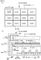
図3に概念図を示すように、透過型のカラー液晶表示装置10は、第1の方向に沿ってM0個、第2の方向に沿ってN0個の、合計M0×N0個の画素が2次元マトリクス状に配列された表示領域11を備えている。ここで、表示領域11を、P×Q個の仮想の表示領域ユニット12に分割したと想定する。各表示領域ユニット12は複数の画素から構成されている。具体的には、例えば、画像表示用解像度としてHD−TV規格を満たすものであり、2次元マトリクス状に配列された画素(ピクセル)の数M0×N0を(M0,N0)で表記したとき、例えば、(1920,1080)である。また、2次元マトリクス状に配列された画素から構成された表示領域11(図3において、一点鎖線で示す)がP×Q個の仮想の表示領域ユニット12(境界を点線で示す)に分割されている。(P,Q)の値は、例えば、(19,12)である。但し、図面の簡素化のため、図3における表示領域ユニット12(及び、後述する面状光源ユニット42)の数は、この値と異なる。各表示領域ユニット12は複数(M×N)の画素から構成されており、1つの表示領域ユニット12を構成する画素の数は、例えば、約1万である。各画素は、それぞれが異なる色を発光する複数の副画素を1組として構成されている。より具体的には、各画素は、赤色発光副画素(副画素[R])、緑色発光副画素(副画素[G])、及び、青色発光副画素(副画素[B])の3つの副画素(サブピクセル)から構成されている。この透過型のカラー液晶表示装置10は、線順次駆動される。より具体的には、カラー液晶表示装置10は、マトリクス状に交差する走査電極(第1の方向に沿って延びている)とデータ電極(第2の方向に沿って延びている)とを有し、走査電極に走査信号を入力して走査電極を選択、走査し、データ電極に入力されたデータ信号(制御信号に基づく信号である)に基づき画像を表示させ、1画面を構成する。
As shown in a conceptual diagram of FIG. 3, the transmissive color liquid crystal display device 10 of the zero M along a first direction, N 0 along the second direction, 0 total M 0 × N Are provided with a
カラー液晶表示装置10は、図6に模式的な一部断面図を示すように、透明第1電極24を備えたフロント・パネル20、透明第2電極34を備えたリア・パネル30、及び、フロント・パネル20とリア・パネル30との間に配された液晶材料13から成る。
The color liquid crystal display device 10 includes a front panel 20 having a transparent first electrode 24, a rear panel 30 having a transparent
フロント・パネル20は、例えば、ガラス基板から成る第1の基板21と、第1の基板21の外面に設けられた偏光フィルム26とから構成されている。第1の基板21の内面には、アクリル樹脂やエポキシ樹脂から成るオーバーコート層23によって被覆されたカラーフィルター22が設けられ、オーバーコート層23上には、透明第1電極(共通電極とも呼ばれ、例えば、ITOから成る)24が形成され、透明第1電極24上には配向膜25が形成されている。一方、リア・パネル30は、より具体的には、例えば、ガラス基板から成る第2の基板31と、第2の基板31の内面に形成されたスイッチング素子(具体的には、薄膜トランジスタ、TFT)32と、スイッチング素子32によって導通/非導通が制御される透明第2電極(画素電極とも呼ばれ、例えば、ITOから成る)34と、第2の基板31の外面に設けられた偏光フィルム36とから構成されている。透明第2電極34を含む全面には配向膜35が形成されている。フロント・パネル20とリア・パネル30とは、それらの外周部で封止材(図示せず)を介して接合されている。尚、スイッチング素子32は、TFTに限定されず、例えば、MIM素子から構成することもできる。また、図面における参照番号37は、スイッチング素子32とスイッチング素子32との間に設けられた絶縁層である。
The front panel 20 includes, for example, a first substrate 21 made of a glass substrate and a
これらの透過型のカラー液晶表示装置を構成する各種の部材や、液晶材料は、周知の部材、材料から構成することができるので、詳細な説明は省略する。 Since various members and liquid crystal materials constituting these transmissive color liquid crystal display devices can be composed of well-known members and materials, detailed description thereof is omitted.
直下型の面状光源装置(バックライト)40は、P×Q個の仮想の表示領域ユニット12に対応したP×Q個の面状光源ユニット42から成り、各面状光源ユニット42は、面状光源ユニット42に対応する表示領域ユニット12を背面から照明する。面状光源ユニット42に備えられた光源は、個別に制御される。尚、カラー液晶表示装置10の下方に面状光源装置40が位置しているが、図3においては、カラー液晶表示装置10と面状光源装置40とを別々に表示した。面状光源装置40における発光ダイオード等の配置、配列状態を図5の(A)に模式的に示し、カラー液晶表示装置10及び面状光源装置40から成る液晶表示装置組立体の模式的な一部断面図を図5の(B)に示す。光源は、パルス幅変調(PWM)制御方式に基づき駆動される発光ダイオード41から成る。
The direct-type planar light source device (backlight) 40 includes P × Q planar
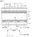
図5の(B)に液晶表示装置組立体の模式的な一部断面図を示すように、面状光源装置40は、外側フレーム53と内側フレーム54とを備えた筐体51から構成されている。そして、透過型のカラー液晶表示装置10の端部は、外側フレーム53と内側フレーム54とによって、スペーサ55A,55Bを介して挟み込まれるように保持されている。また、外側フレーム53と内側フレーム54との間には、ガイド部材56が配置されており、外側フレーム53と内側フレーム54とによって挟み込まれたカラー液晶表示装置10がずれない構造となっている。筐体51の内部であって上部には、拡散板61が、スペーサ55C、ブラケット部材57を介して、内側フレーム54に取り付けられている。また、拡散板61の上には、拡散シート62、プリズムシート63、偏光変換シート64といった光学機能シート群が積層されている。
As shown in a schematic partial cross-sectional view of the liquid crystal display device assembly in FIG. 5B, the planar light source device 40 includes a
筐体51の内部であって下部には、反射シート65が備えられている。ここで、この反射シート65は、その反射面が拡散板61と対向するように配置され、筐体51の底面52Aに図示しない取付け用部材を介して取り付けられている。反射シート65は、例えば、シート基材上に、銀反射膜、低屈折率膜、高屈折率膜を順に積層された構造を有する銀増反射膜から構成することができる。反射シート65は、複数の発光ダイオード41(光源41)から出射された光や、筐体51の側面52B、あるいは、場合によっては、図1の(A)、(B)、図2の(A)、(B)あるいは図5の(A)に示す支持壁44によって反射された光を反射する。こうして、赤色を発光する複数の赤色発光ダイオード41R(光源41R)、緑色を発光する複数の緑色発光ダイオード41G(光源41G)、及び、青色を発光する複数の青色発光ダイオード41B(光源41B)から出射された赤色光、緑色光及び青色光が混色され、色純度の高い白色光を照明光として得ることができる。この照明光は、拡散板61、拡散シート62、プリズムシート63、偏光変換シート64といった光学機能シート群を通過し、カラー液晶表示装置10を背面から照射する。
A reflection sheet 65 is provided inside and below the
筐体51の底面52A近傍には、光センサーであるフォトダイオード43R,43G,43Bが配置されている。尚、フォトダイオード43Rは、赤色光の光強度を測定するために赤色フィルターが取り付けられたフォトダイオードであり、フォトダイオード43Gは、緑色光の光強度を測定するために緑色フィルターが取り付けられたフォトダイオードであり、フォトダイオード43Bは、青色光の光強度を測定するために青色フィルターが取り付けられたフォトダイオードである。ここで、1個の面状光源ユニット42に1組の光センサー(フォトダイオード43R,43G,43B)が配置されている。光センサーであるフォトダイオード43R,43G,43Bによって測定される光源41R,41G,41Bの発光状態は、発光ダイオード41R,41G,41Bの輝度及び色度である。
In the vicinity of the
発光ダイオード41R,41G,41Bの配列状態は、例えば、赤色(例えば、波長640nm)を発光する赤色発光ダイオード41R、緑色(例えば、波長530nm)を発光する緑色発光ダイオード41G、及び、青色(例えば、波長450nm)を発光する青色発光ダイオード41Bを1組とした発光ダイオード・ユニットを水平方向及び垂直方向に複数、並べる配列とすることができる。尚、この場合、1つの面状光源ユニット42に1つの発光ダイオード・ユニットが配置されている。
The arrangement state of the
面状光源装置40を構成する面状光源ユニット42と面状光源ユニット42とは、支持壁44で仕切られている。1つの面状光源ユニット42は、4つの支持壁44によって囲まれ、あるいは又、3つの支持壁44と筐体51の1つの側面52Bによって囲まれ、あるいは又、2つの支持壁44と筐体51の2つの側面52Bによって囲まれている。支持壁44は、筐体51の底面52Aに図示しない取付け用部材を介して取り付けられている。
The planar
図3及び図4に示すように、外部(ディスプレイ回路)からの駆動信号に基づき面状光源装置40及びカラー液晶表示装置10を駆動するための駆動回路は、パルス幅変調制御方式に基づき、面状光源装置40を構成する赤色発光ダイオード41R、緑色発光ダイオード41G及び青色発光ダイオード41Bのオン/オフ制御を行うバックライト制御ユニット70及び面状光源ユニット駆動回路80、並びに、液晶表示装置駆動回路90から構成されている。バックライト制御ユニット70は、演算回路71及び記憶装置(メモリ)72から構成されている。一方、面状光源ユニット駆動回路80は、演算回路81、記憶装置(メモリ)82、LED駆動回路83、フォトダイオード制御回路84、FETから成るスイッチング素子85R,85G,85B、発光ダイオード駆動電源(定電流源)86から構成されている。バックライト制御ユニット70及び面状光源ユニット駆動回路80を構成するこれらの回路等は、周知の回路等とすることができる。一方、カラー液晶表示装置10を駆動するための液晶表示装置駆動回路90は、タイミングコントローラ91といった周知の回路から構成されている。カラー液晶表示装置10には、液晶セルを構成するTFTから成るスイッチング素子32を駆動するための、ゲート・ドライバ、ソース・ドライバ等(これらは図示せず)が備えられている。或る画像表示フレームにおける発光ダイオード41R,41G,41Bの発光状態は、フォトダイオード43R,43G,43Bによって測定され、フォトダイオード43R,43G,43Bからの出力はフォトダイオード制御回路84に入力され、フォトダイオード制御回路84、演算回路81において、発光ダイオード41R,41G,41Bの例えば輝度及び色度としてのデータ(信号)とされ、係るデータがLED駆動回路83に送られ、次の画像表示フレームにおける発光ダイオード41R,41G,41Bの発光状態が制御されるといったフィードバック機構が形成される。また、発光ダイオード41R,41G,41Bの下流には電流検出用の抵抗体rR,rG,rBが、発光ダイオード41R,41G,41Bと直列に挿入されており、抵抗体rR,rG,rBを流れる電流が電圧に変換され、抵抗体rR,rG,rBにおける電圧降下が所定の値となるように、LED駆動回路83の制御下、発光ダイオード駆動電源86の動作が制御される。ここで、図4には、発光ダイオード駆動電源(定電流源)86を1つで描写しているが、実際には、発光ダイオード41R,41G,41Bのそれぞれを駆動するための発光ダイオード駆動電源86が配されている。
As shown in FIGS. 3 and 4, the driving circuit for driving the planar light source device 40 and the color liquid crystal display device 10 based on a driving signal from the outside (display circuit) is based on the pulse width modulation control method.
2次元マトリクス状に配列された画素から構成された表示領域がP×Q個の表示領域ユニットに分割されているが、この状態を、「行」及び「列」で表現すると、Q行×P列の表示領域ユニットに分割されていると云える。また、表示領域ユニット12は複数(M×N)の画素から構成されているが、この状態を、「行」及び「列」で表現すると、N行×M列の画素から構成されていると云える。尚、2次元マトリクス状に配列され、第q行、第p列[但し、q=1,2,・・・,Qであり、p=1,2,・・・,Pである]に位置する表示領域ユニット、面状光源ユニットを、それぞれ、表示領域ユニット12(q,p)、面状光源ユニット42(q,p)と表記し、表示領域ユニット12(q,p)あるいは面状光源ユニット42(q,p)に関連する要素、項目に、添字「(q,p)」あるいは「-(q,p)」を付する場合がある。ここで、赤色発光副画素(副画素[R])、緑色発光副画素(副画素[G])、及び、青色発光副画素(副画素[B])を一括して纏めて『副画素[R,G,B]』と呼ぶ場合があるし、副画素[R,G,B]の動作の制御(具体的には、例えば、光透過率(開口率)の制御)のために副画素[R,G,B]に入力される赤色発光制御信号、緑色発光制御信号、及び、青色発光制御信号を一括して纏めて『制御信号[R,G,B]』と呼ぶ場合があるし、表示領域ユニットを構成する副画素[R,G,B]を駆動するために駆動回路に外部から入力される赤色発光副画素駆動信号、緑色発光副画素駆動信号、及び、青色発光副画素駆動信号を一括して纏めて『駆動信号[R,G,B]』と呼ぶ場合がある。
A display area composed of pixels arranged in a two-dimensional matrix is divided into P × Q display area units. When this state is expressed by “row” and “column”, Q rows × P It can be said that the display area unit is divided into columns. The
各画素は、副画素[R](赤色発光サブピクセル)、副画素[G](緑色発光サブピクセル)、及び、副画素[B](青色発光サブピクセル)の3つの副画素(サブピクセル)を1組として構成されているが、以下の実施例の説明においては、副画素[R,G,B]のそれぞれの輝度の制御(階調制御)を8ビット制御とし、0〜255の28段階にて行うとする。従って、各表示領域ユニット12を構成する各画素における副画素[R,G,B]のそれぞれを駆動するために液晶表示装置駆動回路90に入力される駆動信号[R,G,B]の値xR,xG,xBのそれぞれは、28段階の値をとる。また、各面状光源ユニットを構成する赤色発光ダイオード41R、緑色発光ダイオード41G及び青色発光ダイオード41Bのそれぞれの発光時間を制御するためのパルス幅変調出力信号の値SR,SG,SBも、0〜255の28段階の値をとる。但し、これに限定するものではなく、例えば、10ビット制御とし、0〜1023の210段階にて行うこともでき、この場合には、8ビットの数値での表現を、例えば4倍すればよい。
Each pixel has three subpixels (subpixels): a subpixel [R] (red light emitting subpixel), a subpixel [G] (green light emitting subpixel), and a subpixel [B] (blue light emitting subpixel). However, in the description of the following embodiments, the luminance control (gradation control) of each of the sub-pixels [R, G, B] is 8-bit control, and 2 from 0 to 255. This is done in 8 stages. Therefore, the value of the drive signal [R, G, B] input to the liquid crystal display
画素のそれぞれに、画素のそれぞれの光透過率Ltを制御する制御信号が駆動回路から供給される。具体的には、副画素[R,G,B]のそれぞれに、副画素[R,G,B]のそれぞれの光透過率Ltを制御する制御信号[R,G,B]が液晶表示装置駆動回路90から供給される。即ち、液晶表示装置駆動回路90においては、入力された駆動信号[R,G,B]から制御信号[R,G,B]が生成され、この制御信号[R,G,B]が副画素[R,G,B]に供給(出力)される。尚、面状光源ユニット42の光源輝度Y2を1画像表示フレーム毎に変化させるので、制御信号[R,G,B]は、基本的に、駆動信号[R,G,B]の値を2.2乗した値に対して、光源輝度Y2の変化に基づく補正(補償)を行った値を有する。そして、液晶表示装置駆動回路90を構成するタイミングコントローラ91から、カラー液晶表示装置10のゲート・ドライバ及びソース・ドライバに、制御信号[R,G,B]が周知の方法で送出され、制御信号[R,G,B]に基づき各副画素を構成するスイッチング素子32が駆動され、液晶セルを構成する透明第1電極24及び透明第2電極34に所望の電圧が印加されることで、各副画素の光透過率(開口率)Ltが制御される。ここで、制御信号[R,G,B]の値が大きいほど、副画素[R,G,B]の光透過率(副画素の開口率)Ltが高くなり、副画素[R,G,B]の輝度(表示輝度y)の値が高くなる。即ち、副画素[R,G,B]を通過する光によって構成される画像(通常、一種、点状である)は明るい。
A control signal for controlling the light transmittance Lt of each pixel is supplied from the drive circuit to each pixel. Specifically, a control signal [R, G, B] for controlling the light transmittance Lt of each of the sub-pixels [R, G, B] is transmitted to each of the sub-pixels [R, G, B]. Supplied from the
表示輝度y及び光源輝度Y2の制御は、カラー液晶表示装置10の画像表示における1画像表示フレーム毎、表示領域ユニット毎、面状光源ユニット毎に行われる。また、1画像表示フレーム内におけるカラー液晶表示装置10の動作と面状光源装置40の動作とは同期させられる。尚、駆動回路に電気信号として1秒間に送られる画像情報の数(毎秒画像)がフレーム周波数(フレームレート)であり、フレーム周波数の逆数がフレーム時間(単位:秒)である。 The display brightness y and the light source brightness Y 2 are controlled for each image display frame, each display area unit, and each planar light source unit in the image display of the color liquid crystal display device 10. Further, the operation of the color liquid crystal display device 10 and the operation of the planar light source device 40 within one image display frame are synchronized. Note that the number of image information (images per second) sent to the drive circuit as electrical signals per second is the frame frequency (frame rate), and the inverse of the frame frequency is the frame time (unit: seconds).
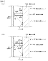
実施例1は、本発明の面状光源装置及び表示装置組立体に関する。実施例1の面状光源装置の部分的な概念図を、図1の(A)に示す。実施例1の面状光源装置40は、2次元マトリクス状に配列された画素から構成された表示領域11を有する透過型のカラー液晶表示装置10を背面から照明する面状光源装置である。そして、実施例1の面状光源装置40は、カラー液晶表示装置10と対面する拡散板61を備えており、複数の面状光源ユニット42から成り、各面状光源ユニット42は光源41(41R,41G,41B)を備えており、面状光源ユニット42と面状光源ユニット42との間には、拡散板61を支持するための支持壁44が配設されており、支持壁44の頂面45は、拡散板61に近接している。
Example 1 relates to a planar light source device and a display device assembly of the present invention. A partial conceptual diagram of the planar light source device of Example 1 is shown in FIG. The planar light source device 40 according to the first embodiment is a planar light source device that illuminates a transmissive color liquid crystal display device 10 having a
具体的には、図1の(A)に部分的な概念図を示すように、カラー液晶表示装置10の使用時には、カラー液晶表示装置10は略垂直に配置されるので、この状態にあっては、支持壁44の頂面45と拡散板61とは接触しておらず、拡散板61と支持壁44の頂面45との間には、1.0mm以下の隙間が存在する。一方、面状光源装置の製造時、あるいは、液晶表示装置と面状光源装置との組立工程等において、面状光源装置を水平に保持した状態になった場合、拡散板61が撓む結果、拡散板61と支持壁44の頂面45とは面状にて接触する場合がある。尚、図1の(A)、(B)、及び、図2の(A)、(B)においては、光源41、筐体51の底面52A、及び、拡散板61を明示するために、これらに斜線を付した。
Specifically, as shown in a partial conceptual diagram in FIG. 1A, when the color liquid crystal display device 10 is used, the color liquid crystal display device 10 is disposed substantially vertically. The
ここで、実施例1にあっては、複数の面状光源ユニット42は、カラー液晶表示装置10の表示領域11をP×Q個の仮想の表示領域ユニット12に分割したと想定したときのこれらのP×Q個の表示領域ユニット12に対応したP×Q個の面状光源ユニット42から成り、面状光源ユニット42に備えられた光源41(41R,41G,41B)は、個別に制御される。但し、面状光源ユニット42の光源輝度は、他の面状光源ユニット42に備えられた光源41(41R,41G,41B)の発光状態等による影響を受けるので、この影響を考慮した上で、光源41の発光状態を制御することが望ましい。
Here, in Example 1, it is assumed that the plurality of planar
そして、面状光源ユニット42に備えられた光源41から出射され、光源41と対面する支持壁の第1の側面46Aにおいて拡散され、支持壁44の第1の側面46Aから支持壁44の内部に入射した光(点線で示す)は、第1の側面46Aと対向する支持壁44の第2の側面46B及び支持壁44の頂面45から出射される。これによって、支持壁44の影が発生し難く、従って、拡散板61に輝度ムラが生じ易いといった問題の発生を回避することができる。
Then, the light is emitted from the light source 41 provided in the planar
実施例1にあっては、支持壁44は、面状光源ユニット42に備えられた光源41から出射された光に対して透明な材料、具体的には、アクリル系樹脂から成り、支持壁44の第1の側面46A及び第2の側面46Bの少なくとも上部には(より具体的には全面に)、サンドブラスト法に基づき、凹凸が形成されている。
In the first embodiment, the
実施例1、あるいは、後述する実施例2〜実施例4にあっては、画素のそれぞれに、画素のそれぞれの光透過率Ltを制御する制御信号が駆動回路から供給される。より具体的には、各画素を構成する副画素[R,G,B]のそれぞれに、副画素[R,G,B]のそれぞれの光透過率Ltを制御する制御信号[R,G,B]が駆動回路90から供給される。そして、面状光源ユニット42(q,p)のそれぞれにおいて、各表示領域ユニット12(q,p)を構成する全ての画素(副画素[R,G,B](q,p))を駆動するために駆動回路70,80(q,p),90に入力される駆動信号[R,G,B](q,p)の値xR-(q,p),xG-(q,p),xB-(q,p)の内の最大値である表示領域ユニット内・駆動信号最大値xU-max(q,p)に等しい値を有する駆動信号に相当する制御信号が画素に供給されたと想定したときの画素(副画素[R,G,B](q,p))の輝度(光透過率・第1規定値Lt1における表示輝度・第2規定値y2-(q,p))が得られるように、この表示領域ユニット12(q,p)に対応する面状光源ユニット42(q,p)を構成する光源41(q,p)の輝度を面状光源ユニット駆動回路80(q,p)によって制御する。
In Embodiment 1 or Embodiments 2 to 4 to be described later, a control signal for controlling the light transmittance Lt of each pixel is supplied from the drive circuit to each pixel. More specifically, a control signal [R, G, B] that controls the light transmittance Lt of each of the sub-pixels [R, G, B] is supplied to each of the sub-pixels [R, G, B] constituting each pixel. B] is supplied from the
以下、実施例1、あるいは、後述する実施例2〜実施例4における液晶表示装置組立体の駆動方法を、図3及び図4を参照して説明する。 Hereinafter, the driving method of the liquid crystal display device assembly according to the first embodiment or the second to fourth embodiments described later will be described with reference to FIGS.
[ステップ−100]
スキャンコンバータ等の周知のディスプレイ回路から送出された1画像表示フレーム分の駆動信号[R,G,B]及びクロック信号CLKは、バックライト制御ユニット70及び液晶表示装置駆動回路90に入力される(図3参照)。尚、駆動信号[R,G,B]は、例えば撮像管への入力光量をy’としたとき、撮像管からの出力信号であり、例えば放送局等から出力され、画素の光透過率Ltを制御するために液晶表示装置駆動回路90にも入力される駆動信号であり、入力光量y’の0.45乗の関数で表すことができる。そして、バックライト制御ユニット70に入力された1画像表示フレーム分の駆動信号[R,G,B]の値xR,xG,xBは、バックライト制御ユニット70を構成する記憶装置(メモリ)72に、一旦、記憶される。また、液晶表示装置駆動回路90に入力された1画像表示フレーム分の駆動信号[R,G,B]の値xR,xG,xBも、液晶表示装置駆動回路90を構成する記憶装置(図示せず)に、一旦、記憶される。
[Step-100]
The drive signal [R, G, B] and the clock signal CLK for one image display frame sent from a known display circuit such as a scan converter are input to the
[ステップ−110]
次いで、バックライト制御ユニット70を構成する演算回路71においては、記憶装置72に記憶された駆動信号[R,G,B]の値を読み出し、第(p,q)番目[但し、先ず、p=1,q=1]の表示領域ユニット12(q,p)において、この第(p,q)番目の表示領域ユニット12(q,p)を構成する全ての画素における副画素[R,G,B](q,p)を駆動するための駆動信号[R,G,B](q,p)の値xR-(q,p),xG-(q,p),xB-(q,p)の内の最大値である表示領域ユニット内・駆動信号最大値xU-max(q,p)を、演算回路71において求める。そして、表示領域ユニット内・駆動信号最大値xU-max(q,p)を、記憶装置72に記憶する。このステップを、m=1,2,・・・,M、n=1,2,・・・,Nの全てに対して、即ち、M×N個の画素に対して、実行する。
[Step-110]
Next, in the
例えば、xR-(q,p)が「110」に相当する値であり、xG-(q,p)が「150」に相当する値であり、xB-(q,p)が「50」に相当する値である場合、xU-max(q,p)は「150」に相当する値である。 For example, x R- (q, p) is a value corresponding to “110”, x G- (q, p) is a value corresponding to “150”, and x B- (q, p) is “ In the case of a value corresponding to “50”, x U−max (q, p) is a value corresponding to “150”.
この操作を、(p,q)=(1,1)から(P,Q)まで繰り返し、全ての表示領域ユニット12(q,p)における表示領域ユニット内・駆動信号最大値xU-max(q,p)を、記憶装置72に記憶する。
This operation is repeated from (p, q) = (1, 1) to (P, Q), and the display area unit internal drive signal maximum value x U-max (in all
そして、表示領域ユニット内・駆動信号最大値xU-max(q,p)に等しい値を有する駆動信号[R,G,B](q,p)に相当する制御信号[R,G,B](q,p)が副画素[R,G,B](q,p)に供給されたと想定したときの輝度(光透過率・第1規定値Lt1における表示輝度・第2規定値y2-(q,p))が面状光源ユニット42(q,p)によって得られるように、表示領域ユニット12(q,p)に対応する面状光源ユニット42(q,p)の光源輝度Y2-(q,p)を、面状光源ユニット駆動回路80(q,p)の制御下、増減する。具体的には、以下の式(1)を満足するように、1画像表示フレーム毎、1面状光源ユニット毎に光源輝度Y2を制御すればよい。より具体的には、光源輝度制御関数g(xnol-max)である式(2)に基づき光源41(q,p)の輝度を制御し、且つ、式(1)を満足するように光源輝度Y2を制御すればよい。このような制御の概念図を、図7の(A)及び(B)に示す。但し、後述するように、他の面状光源ユニット42の影響に基づいた補正を、光源輝度Y2に対して施す必要がある。尚、光源輝度Y2の制御に関するこれらの関係、即ち、表示領域ユニット内・駆動信号最大値xU-max、この最大値xU-maxに等しい値を有する駆動信号に相当する制御信号の値、このような制御信号が画素(副画素)に供給されたと想定したときの表示輝度・第2規定値y2、このときの各副画素の光透過率(開口率)[光透過率・第2規定値Lt2]、各副画素の光透過率(開口率)を光透過率・第1規定値Lt1としたときに表示輝度・第2規定値y2が得られるような面状光源ユニットにおける輝度制御パラメータの関係は、予め求めておき、記憶装置72等に記憶しておけばよい。
Then, the control signal [R, G, B corresponding to the drive signal [R, G, B] (q, p) having a value equal to the in-display area unit / maximum drive signal value x U-max (q, p). ] (Q, p) is assumed to be supplied to the sub-pixel [R, G, B] (q, p) (light transmittance, display brightness at the first specified value Lt 1 , second specified value y) 2- (q, p)) as obtained by the surface
Y2・Lt1=Y1・Lt2 (1)
g(xnol-max)=a1・(xnol-max)2.2+a0 (2)
Y 2 · Lt 1 = Y 1 · Lt 2 (1)
g (x nol-max ) = a 1 · (x nol-max ) 2.2 + a 0 (2)
ここで、画素(あるいは、画素を構成する副画素[R,G,B]のそれぞれ)を駆動するために液晶表示装置駆動回路90に入力される駆動信号(駆動信号[R,G,B])の最大値をxmaxとしたとき、
xnol-max≡xU-max/xmax
であり、a1,a0は定数であり、
a1+a0=1
0<a0<1,0<a1<1
で表すことができる。例えば、
a1=0.99
a0=0.01
とすればよい。また、駆動信号[R,G,B]の値xR,xG,xBのそれぞれは、28段階の値をとるので、xmaxの値は「255」に相当する値である。
Here, driving signals (driving signals [R, G, B]) input to the liquid crystal display
x nol-max ≡ x U-max / x max
And a 1 and a 0 are constants,
a 1 + a 0 = 1
0 <a 0 <1, 0 <a 1 <1
Can be expressed as For example,
a 1 = 0.99
a 0 = 0.01
And it is sufficient. The value x R of the drive signals [R, G, B], x G, each x B, and takes a value of 2 8 steps, the value of x max is a value corresponding to "255".
ところで、面状光源装置にあっては、例えば、(p,q)=(1,1)の面状光源ユニット42(1,1)の輝度制御を想定した場合、他のP×Q個の面状光源ユニット42からの影響を考慮する必要がある。このような面状光源ユニット42が他の面状光源ユニット42から受ける影響は、各面状光源ユニット42の発光プロファイルによって予め判明しているので、逆算によって差分を計算でき、その結果、補正が可能である。演算の基本形を以下に説明する。
By the way, in the planar light source device, for example, assuming brightness control of the planar
式(1)及び式(2)の要請に基づくP×Q個の面状光源ユニット42に要求される輝度(光源輝度Y2)を行列[LPxQ]で表す。また、或る面状光源ユニットのみを駆動し、他の面状光源ユニットは駆動していないときに得られる或る面状光源ユニットの輝度を、P×Q個の面状光源ユニット42に対して予め求めておく。係る輝度を行列[L’PxQ]で表す。更には、補正係数を行列[αPxQ]で表す。すると、これらの行列の関係は、以下の式(3−1)で表すことができる。補正係数の行列[αPxQ]は、予め求めておくことができる。
[LPxQ]=[L’PxQ]・[αPxQ] (3−1)
よって、式(3−1)から行列[L’PxQ]を求めればよい。行列[L’PxQ]は、逆行列の演算から求めることができる。即ち、
[L’PxQ]=[LPxQ]・[αPxQ]-1 (3−2)
を計算すればよい。そして、行列[L’PxQ]で表された輝度が得られるように光源41(q,p)を制御すればよく、具体的には、係る操作、処理は、記憶装置(メモリ)82に記憶された情報(データテーブル)を用いて行えばよい。尚、光源41(q,p)の制御にあっては、行列[L’PxQ]の値は負の値を取れないので、演算結果は正の領域にとどめる必要があることは云うまでもない。従って、式(3−2)の解は厳密解ではなく、近似解となる場合がある。
The luminance (light source luminance Y 2 ) required for the P × Q planar
[L PxQ ] = [L ′ PxQ ] · [α PxQ ] (3-1)
Therefore, what is necessary is just to obtain | require matrix [L' PxQ ] from Formula (3-1). The matrix [L ′ PxQ ] can be obtained from the inverse matrix operation. That is,
[L ′ PxQ ] = [L PxQ ] · [α PxQ ] −1 (3-2)
Should be calculated. Then, the light source 41 (q, p) may be controlled so that the luminance represented by the matrix [L ′ PxQ ] is obtained. Specifically, the operation and processing are stored in the storage device (memory) 82. What is necessary is just to perform using the information (data table). In the control of the light source 41 (q, p) , since the value of the matrix [L ′ PxQ ] cannot take a negative value, it is needless to say that the calculation result needs to be kept in a positive region. . Therefore, the solution of equation (3-2) may not be an exact solution but an approximate solution.
このように、バックライト制御ユニット70を構成する演算回路71において得られた式(1)及び式(2)の値に基づき得られた行列[LPxQ]、補正係数の行列[αPxQ]に基づき、上述したとおり、面状光源ユニットを単独で駆動したと想定したときの輝度の行列[L’PxQ]を求め、更には、記憶装置72に記憶された変換テーブルに基づき、0〜255の範囲内の対応する整数に変換する。こうして、バックライト制御ユニット70を構成する演算回路71において、面状光源ユニット42(q,p)における赤色発光ダイオード41R(q,p)の発光時間を制御するためのパルス幅変調出力信号の値SR-(q,p)、緑色発光ダイオード41G(q,p)の発光時間を制御するためのパルス幅変調出力信号の値SG-(q,p)、青色発光ダイオード41B(q,p)の発光時間を制御するためのパルス幅変調出力信号の値SB-(q,p)を得ることができる。
As described above, the matrix [L PxQ ] and the correction coefficient matrix [α PxQ ] obtained based on the values of the equations (1) and (2) obtained in the
[ステップ−120]
次に、バックライト制御ユニット70を構成する演算回路71において得られたパルス幅変調出力信号の値SR-(q,p),SG-(q,p),SB-(q,p)は、面状光源ユニット42(q,p)に対応して設けられた面状光源ユニット駆動回路80(q,p)の記憶装置82に送出され、記憶装置82において記憶される。また、クロック信号CLKも面状光源ユニット駆動回路80(q,p)に送出される(図4参照)。
[Step-120]
Next, the values S R- (q, p) , S G- (q, p) , S B- (q, p ) of the pulse width modulation output signal obtained in the
[ステップ−130]
そして、パルス幅変調出力信号の値SR-(q,p),SG-(q,p),SB-(q,p)に基づき、面状光源ユニット42(q,p)を構成する赤色発光ダイオード41R(q,p)のオン時間tR-ON及びオフ時間tR-OFF、緑色発光ダイオード41G(q,p)のオン時間tG-ON及びオフ時間tG-OFF、青色発光ダイオード41B(q,p)のオン時間tB-ON及びオフ時間tB-OFFを演算回路81は決定する。尚、
tR-ON+tR-OFF=tG-ON+tG-OFF=tB-ON+tB-OFF=一定値tConst
である。また、発光ダイオードのパルス幅変調に基づく駆動におけるデューティ比は、
tON/(tON+tOFF)=tON/tConst
で表すことができる。
[Step-130]
Then, the planar
t R-ON + t R-OFF = t G-ON + t G-OFF = t B-ON + t B-OFF = constant value t Const
It is. The duty ratio in driving based on pulse width modulation of the light emitting diode is
t ON / (t ON + t OFF ) = t ON / t Const
Can be expressed as
そして、面状光源ユニット42(q,p)を構成する赤色発光ダイオード41R(q,p),緑色発光ダイオード41G(q,p)、青色発光ダイオード41B(q,p)のオン時間tR-ON-(q,p),tG-ON-(q,p),tB-ON-(q,p)に相当する信号が、LED駆動回路83に送られ、このLED駆動回路83から、オン時間tR-ON-(q,p),tG-ON-(q,p),tB-ON-(q,p)に相当する信号の値に基づき、スイッチング素子85R(q,p),85G(q,p),85B(q,p)が、オン時間tR-ON-(q,p),tG-ON-(q,p),tB-ON-(q,p)だけオン状態となり、発光ダイオード駆動電源86からのLED駆動電流が、各発光ダイオード41R(q,p),41G(q,p),41B(q,p)に流される。その結果、各発光ダイオード41R(q,p),41G(q,p),41B(q,p)は、1画像表示フレームにおいて、オン時間tR-ON-(q,p),tG-ON-(q,p),tB-ON-(q,p)だけ発光する。こうして、第(p,q)番目の表示領域ユニット12(q,p)を、所定の照度において照明する。
The on-time t R− of the red
こうして得られた状態を、図8の(A)及び(B)に実線で示すが、図8の(A)は、副画素を駆動するために液晶表示装置駆動回路90に入力される駆動信号の値を2.2乗した値(x’≡x2.2)とデューティ比(=tON/tConst)との関係を模式的に示す図であり、図8の(B)は、副画素の光透過率Ltを制御するための制御信号の値Xと表示輝度yとの関係を模式的に示す図である。
The states obtained in this way are indicated by solid lines in FIGS. 8A and 8B. FIG. 8A shows a drive signal input to the liquid crystal display
一方、液晶表示装置駆動回路90に入力された駆動信号[R,G,B](q,p)の値xR-(q,p),xG-(q,p),xB-(q,p)はタイミングコントローラ91へ送られ、タイミングコントローラ91にあっては、入力された駆動信号[R,G,B](q,p)に相当する制御信号[R,G,B](q,p)を、副画素[R,G,B](q,p)に供給(出力)する。液晶表示装置駆動回路90のタイミングコントローラ91において生成され、液晶表示装置駆動回路90から副画素[R,G,B](q,p)に供給される制御信号[R,G,B](q,p)の値XR-(q,p),XG-(q,p),XB-(q,p)と、駆動信号[R,G,B](q,p)の値xR-(q,p),xG-(q,p),xB-(q,p)とは、以下の式(4−1)、式(4−2)、式(4−3)の関係にある。但し、b1_R,b0_R,b1_G,b0_G,b1_B,b0_Bは定数である。また、面状光源ユニット42(q,p)の光源輝度Y2-(q,p)を画像表示フレーム毎に変化させるので、制御信号[R,G,B](q,p)は、基本的に、駆動信号[R,G,B](q,p)の値を2.2乗した値に対して、光源輝度Y2-(q,p)の変化に基づく補正(補償)を行った値を有する。即ち、実施例にあっては、1画像表示フレーム毎に光源輝度Y2-(q,p)が変化するので、光源輝度Y2-(q,p)(≦Y1)において表示輝度・第2規定値y2-(q,p)が得られるように制御信号[R,G,B](q,p)の値XR-(q,p),XG-(q,p),XB-(q,p)を決定、補正(補償)して、画素あるいは副画素の光透過率(開口率)Ltを制御している。ここで、式(4−1)、式(4−2)、式(4−3)の関数fR,fG,fBは、係る補正(補償)を行うための予め求められた関数である。
On the other hand, the values x R- (q, p) , x G- (q, p) , x B- ( ) of the drive signals [R, G, B] (q, p) input to the liquid crystal display
XR-(q,p)=fR(b1_R・xR-(q,p) 2.2+b0_R) (4−1)
XG-(q,p)=fG(b1_G・xG-(q,p) 2.2+b0_G) (4−2)
XB-(q,p)=fB(b1_B・xB-(q,p) 2.2+b0_B) (4−3)
X R- (q, p) = f R (b 1_R · x R- (q, p) 2.2 + b 0_R) (4-1)
X G- (q, p) = f G (b 1_G · x G- (q, p) 2.2 + b 0_G) (4-2)
X B- (q, p) = f B (b 1_B · x B- (q, p) 2.2 + b 0_B) (4-3)
こうして、1画像表示フレームにおける画像表示動作が完了する。 Thus, the image display operation in one image display frame is completed.
実施例2は、実施例1の変形である。実施例2にあっては、図1の(B)に部分的な概念図を示すように、凹凸は、支持壁44の第1の側面46A及び第2の側面46Bの上部に形成されており、支持壁44の第1の側面46A及び第2の側面46Bの残りの部分には、光反射層47が形成されている。より具体的には、銀反射膜、低屈折率膜、高屈折率膜を順に積層された構造を有する銀増反射シートを、接着剤を用いて、支持壁44の第1の側面46A及び第2の側面46Bの残りの部分に貼り付ければよい。
The second embodiment is a modification of the first embodiment. In Example 2, as shown in a partial conceptual diagram in FIG. 1B, the unevenness is formed on the upper part of the
実施例3も、実施例1の変形である。実施例3にあっては、実施例1と同様に、支持壁44は、面状光源ユニット42に備えられた光源41から出射された光に対して透明な材料から成る。但し、実施例1と異なり、図2の(A)に部分的な概念図を示すように、支持壁44の第1の側面46A及び第2の側面46Bの少なくとも上部には、より具体的には、全面には、光透過・拡散フィルム48が接着剤を用いて貼り付けられている。
The third embodiment is also a modification of the first embodiment. In the third embodiment, as in the first embodiment, the
実施例4は、実施例3の変形である。実施例4にあっては、図2の(B)に部分的な概念図を示すように、光透過・拡散フィルム48は、支持壁44の第1の側面46A及び第2の側面46Bの上部に貼り付けられており、支持壁44の第1の側面46A及び第2の側面46Bの残りの部分には、光反射層49が形成されている。より具体的には、銀増反射シートを、接着剤を用いて、支持壁44の第1の側面46A及び第2の側面46Bの残りの部分に貼り付ければよい。
The fourth embodiment is a modification of the third embodiment. In Example 4, as shown in a partial conceptual diagram in FIG. 2B, the light transmission /
以上、本発明を好ましい実施例に基づき説明したが、本発明はこれらの実施例に限定されるものではない。実施例において説明した透過型のカラー液晶表示装置や面状光源装置、面状光源ユニット、液晶表示装置組立体、駆動回路の構成、構造は例示であるし、これらを構成する部材、材料等も例示であり、適宜、変更することができる。発光ダイオードの温度を温度センサーで監視し、その結果を、面状光源ユニット駆動回路80にフィードバックすることで、面状光源ユニット42の輝度補償(補正)や温度制御を行ってもよい。実施例においては、液晶表示装置の表示領域をP×Q個の仮想の表示領域ユニットに分割したと想定して説明を行ったが、場合によっては、透過型の液晶表示装置は、P×Q個の実際の表示領域ユニットに分割された構造を有していてもよい。更には、支持壁の頂面は、平坦であってもよいし、拡散板に向かって凸の形状(支持壁の高さ方向をZ方向、支持壁の厚さ方向をX方向としたとき、XZ平面で切断したときの断面形状が、楕円、円、半長円形、放物線、3次以上の多項式に例示される曲線の一部、あるいは、釣鐘形状等)を有していてもよい。
As mentioned above, although this invention was demonstrated based on the preferable Example, this invention is not limited to these Examples. The configurations and structures of the transmissive color liquid crystal display device, the planar light source device, the planar light source unit, the liquid crystal display device assembly, and the drive circuit described in the embodiments are examples, and members, materials, and the like constituting these are also examples. This is an example, and can be changed as appropriate. Luminance compensation (correction) and temperature control of the planar
10・・・カラー液晶表示装置、11・・・表示領域、12・・・表示領域ユニット、13・・・液晶材料、20・・・フロント・パネル、21・・・第1の基板、22・・・カラーフィルター、23・・・オーバーコート層、24・・・透明第1電極、25・・・配向膜、26・・・偏光フィルム、30・・・リア・パネル、31・・・第2の基板、32・・・スイッチング素子、34・・・透明第2電極、35・・・配向膜、36・・・偏光フィルム、37・・・絶縁層、40・・・面状光源装置、41,41R,41G,41B・・・発光ダイオード(光源)、42・・・面状光源ユニット、43,43R,43G,43B・・・フォトダイオード(光センサー)、44・・・支持壁、45・・・支持壁の頂面、46A,46B・・・支持壁の側面、47,49・・・光反射層、48・・・光透過・拡散フィルム、51・・・筐体、52A・・・筐体の底面、52B・・・筐体の側面、53・・・外側フレーム、54・・・内側フレーム、55A,55B・・・スペーサ、56・・・ガイド部材、57・・・ブラケット部材、61・・・拡散板、62・・・拡散シート、63・・・プリズムシート、64・・・偏光変換シート、65・・・反射シート、70・・・バックライト制御ユニット、71・・・演算回路、72・・・記憶装置(メモリ)、80・・・面状光源ユニット駆動回路、81・・・演算回路、82・・・記憶装置(メモリ)、83・・・LED駆動回路、84・・・フォトダイオード制御回路、85R,85G,85B・・・スイッチング素子、86・・・発光ダイオード駆動電源、90・・・液晶表示装置駆動回路、91・・・タイミングコントローラ
DESCRIPTION OF SYMBOLS 10 ... Color liquid crystal display device, 11 ... Display area, 12 ... Display area unit, 13 ... Liquid crystal material, 20 ... Front panel, 21 ... 1st board | substrate, 22. .... Color filter, 23 ... Overcoat layer, 24 ... Transparent first electrode, 25 ... Alignment film, 26 ... Polarizing film, 30 ... Rear panel, 31 ... Second 32 ... switching
Claims (7)
液晶表示装置と対面する拡散板を備えており、
複数の面状光源ユニットから成り、
各面状光源ユニットは光源を備えており、
面状光源ユニットと面状光源ユニットとの間には、拡散板を支持するための支持壁が配設されており、
支持壁の頂面は、拡散板に近接しており、
面状光源ユニットに備えられた光源から出射され、光源と対面する支持壁の第1の側面において拡散され、支持壁の第1の側面から支持壁内部に入射した光は、第1の側面と対向する支持壁の第2の側面及び支持壁の頂面から出射される面状光源装置。 A planar light source device for illuminating a transmissive liquid crystal display device having a display area composed of pixels arranged in a two-dimensional matrix from the back,
It has a diffusion plate that faces the liquid crystal display device,
Consisting of a plurality of planar light source units,
Each planar light source unit has a light source,
Between the planar light source unit and the planar light source unit, a support wall for supporting the diffusion plate is disposed,
The top surface of the support wall is close to the diffuser ,
The light emitted from the light source provided in the planar light source unit, diffused on the first side surface of the support wall facing the light source, and incident on the inside of the support wall from the first side surface of the support wall is A planar light source device that emits light from the second side surface of the opposing support wall and the top surface of the support wall .
面状光源ユニットに備えられた光源は、個別に制御される請求項1に記載の面状光源装置。 The plurality of planar light source units includes P × Q pieces corresponding to the P × Q display area units when it is assumed that the display area of the liquid crystal display device is divided into P × Q virtual display area units. Consisting of a planar light source unit
The planar light source device according to claim 1, wherein light sources provided in the planar light source unit are individually controlled.
支持壁の第1の側面及び第2の側面の少なくとも上部には、凹凸が形成されている請求項1に記載の面状光源装置。 The support wall is made of a material transparent to the light emitted from the light source provided in the planar light source unit,
The planar light source device according to claim 1 , wherein irregularities are formed on at least an upper portion of the first side surface and the second side surface of the support wall.
支持壁の第1の側面及び第2の側面の残りの部分には、光反射層が形成されている請求項3に記載の面状光源装置。 The irregularities are formed on the first side surface and the second side surface of the support wall,
The planar light source device according to claim 3 , wherein a light reflecting layer is formed on the remaining portions of the first side surface and the second side surface of the support wall.
支持壁の第1の側面及び第2の側面の少なくとも上部には、光透過・拡散フィルムが貼り付けられている請求項1に記載の面状光源装置。 The support wall is made of a material transparent to the light emitted from the light source provided in the planar light source unit,
The planar light source device according to claim 1 , wherein a light transmission / diffusion film is attached to at least an upper portion of the first side surface and the second side surface of the support wall.
支持壁の第1の側面及び第2の側面の残りの部分には、光反射層が形成されている請求項5に記載の面状光源装置。 The light transmission / diffusion film is affixed on the first side and the second side of the support wall,
The planar light source device according to claim 5 , wherein a light reflecting layer is formed on the remaining portions of the first side surface and the second side surface of the support wall.
該液晶表示装置を背面から照明する面状光源装置、
を備えた表示装置組立体であって、
面状光源装置は、液晶表示装置と対面する拡散板を備えており、複数の面状光源ユニットから成り、
各面状光源ユニットは光源を備えており、
面状光源ユニットと面状光源ユニットとの間には、拡散板を支持するための支持壁が配設されており、
支持壁の頂面は、拡散板に近接しており、
面状光源ユニットに備えられた光源から出射され、光源と対面する支持壁の第1の側面において拡散され、支持壁の第1の側面から支持壁内部に入射した光は、第1の側面と対向する支持壁の第2の側面及び支持壁の頂面から出射される表示装置組立体。 A transmissive liquid crystal display device having a display area composed of pixels arranged in a two-dimensional matrix, and
A planar light source device for illuminating the liquid crystal display device from the back;
A display device assembly comprising:
The planar light source device includes a diffusion plate facing the liquid crystal display device, and includes a plurality of planar light source units.
Each planar light source unit has a light source,
Between the planar light source unit and the planar light source unit, a support wall for supporting the diffusion plate is disposed,
The top surface of the support wall is close to the diffuser ,
The light emitted from the light source provided in the planar light source unit, diffused on the first side surface of the support wall facing the light source, and incident on the inside of the support wall from the first side surface of the support wall is A display device assembly emitted from the second side surface of the opposing support wall and the top surface of the support wall .
Priority Applications (2)
| Application Number | Priority Date | Filing Date | Title |
|---|---|---|---|
| JP2006154982A JP4640264B2 (en) | 2006-06-02 | 2006-06-02 | Planar light source device and display device assembly |
| US11/807,565 US7760291B2 (en) | 2006-06-02 | 2007-05-29 | Planar light-source apparatus |
Applications Claiming Priority (1)
| Application Number | Priority Date | Filing Date | Title |
|---|---|---|---|
| JP2006154982A JP4640264B2 (en) | 2006-06-02 | 2006-06-02 | Planar light source device and display device assembly |
Publications (3)
| Publication Number | Publication Date |
|---|---|
| JP2007324048A JP2007324048A (en) | 2007-12-13 |
| JP2007324048A5 JP2007324048A5 (en) | 2009-06-25 |
| JP4640264B2 true JP4640264B2 (en) | 2011-03-02 |
Family
ID=38856660
Family Applications (1)
| Application Number | Title | Priority Date | Filing Date |
|---|---|---|---|
| JP2006154982A Active JP4640264B2 (en) | 2006-06-02 | 2006-06-02 | Planar light source device and display device assembly |
Country Status (2)
| Country | Link |
|---|---|
| US (1) | US7760291B2 (en) |
| JP (1) | JP4640264B2 (en) |
Families Citing this family (22)
| Publication number | Priority date | Publication date | Assignee | Title |
|---|---|---|---|---|
| JP2008020532A (en) * | 2006-07-11 | 2008-01-31 | Fujifilm Corp | Optical functional sheet and display device |
| JP4455620B2 (en) * | 2007-07-17 | 2010-04-21 | 東芝モバイルディスプレイ株式会社 | Display device manufacturing method and color balance adjusting method |
| TWI368792B (en) * | 2007-11-09 | 2012-07-21 | Au Optronics Corp | Lcd device, backlight module, thereof, with partition wall and method for manufacturing the same |
| BR112012001374A2 (en) * | 2009-07-21 | 2016-03-15 | Sharp Kk | lens unit, light emitting module, lighting device, display device and television receiver. |
| KR101948139B1 (en) * | 2011-12-20 | 2019-02-15 | 엘지이노텍 주식회사 | backlight unit and illumination system using the same |
| CN102661538B (en) * | 2012-04-16 | 2014-10-01 | 深圳市华星光电技术有限公司 | Direct type backlight module group and liquid crystal display device |
| CN103472624B (en) * | 2012-04-16 | 2015-09-30 | 深圳市华星光电技术有限公司 | A kind of down straight aphototropism mode set and liquid crystal indicator |
| US9063367B2 (en) * | 2012-06-19 | 2015-06-23 | Shenzhen China Star Optoelectronics Technology Co., Ltd. | Direct-type backlight unit and liquid crystal display using the same |
| CN102748666B (en) * | 2012-06-19 | 2014-08-27 | 深圳市华星光电技术有限公司 | Direct type backlight module and liquid crystal displayer |
| CN102748667B (en) * | 2012-06-20 | 2014-06-11 | 深圳市华星光电技术有限公司 | Straight-down type backlight module and liquid crystal display thereof |
| JP2014013690A (en) * | 2012-07-04 | 2014-01-23 | Sony Corp | Display device |
| JP6039337B2 (en) * | 2012-09-28 | 2016-12-07 | キヤノン株式会社 | Display device and control method thereof |
| KR101326299B1 (en) * | 2013-01-31 | 2013-11-11 | 삼성전자주식회사 | Display module and displyay apparatus having the same |
| JP6277630B2 (en) * | 2013-08-19 | 2018-02-14 | 船井電機株式会社 | Display device |
| CN104706334B (en) * | 2015-03-30 | 2017-08-11 | 京东方科技集团股份有限公司 | A kind of display panel and display device with health monitoring function |
| US10600213B2 (en) * | 2016-02-27 | 2020-03-24 | Focal Sharp, Inc. | Method and apparatus for color-preserving spectrum reshape |
| US10144288B2 (en) * | 2016-03-31 | 2018-12-04 | Denso International America, Inc. | LCD display with highlighting |
| CN109844401A (en) * | 2016-10-26 | 2019-06-04 | 夏普株式会社 | Lighting device and display device |
| JP2022074264A (en) * | 2020-11-04 | 2022-05-18 | 株式会社ジャパンディスプレイ | Display device |
| CN112558355A (en) * | 2020-12-17 | 2021-03-26 | 业成科技(成都)有限公司 | Backlight module and display panel |
| DE102022205083A1 (en) | 2022-05-20 | 2023-11-23 | Continental Automotive Technologies GmbH | Display device and means of transport |
| US11879633B1 (en) * | 2023-02-10 | 2024-01-23 | Amtran Technology Co., Ltd. | Display device and its back light module and support column |
Citations (7)
| Publication number | Priority date | Publication date | Assignee | Title |
|---|---|---|---|---|
| JP2001272652A (en) * | 2000-03-28 | 2001-10-05 | Toshiba Corp | Display device |
| JP2004264452A (en) * | 2003-02-28 | 2004-09-24 | Fujitsu Kasei Kk | Backlight device |
| JP2005070690A (en) * | 2003-08-28 | 2005-03-17 | Matsushita Electric Ind Co Ltd | Liquid crystal display device |
| JP2005196170A (en) * | 2003-12-30 | 2005-07-21 | Au Optronics Corp | Backlight module supporting structure of liquid crystal display and backlight module equipped with same |
| JP2005203164A (en) * | 2004-01-14 | 2005-07-28 | Progress:Kk | Backlight unit for liquid crystal display device |
| JP2005208408A (en) * | 2004-01-23 | 2005-08-04 | Nec Lcd Technologies Ltd | Direct backlight and display device |
| JP2005310997A (en) * | 2004-04-20 | 2005-11-04 | Sony Corp | Led driving device, back light optical source apparatus, and color liquid crystal display device |
Family Cites Families (3)
| Publication number | Priority date | Publication date | Assignee | Title |
|---|---|---|---|---|
| WO2006003913A1 (en) * | 2004-07-06 | 2006-01-12 | Asagicreate Co., Ltd. | Surface light source and electrically illuminated signboard |
| EP2463707A1 (en) * | 2004-10-19 | 2012-06-13 | Sharp Kabushiki Kaisha | Liquid crystal display device and electronic device using the same |
| KR20060104078A (en) * | 2005-03-29 | 2006-10-09 | 삼성전자주식회사 | Backlight unit and liquid crystal display having the same |
-
2006
- 2006-06-02 JP JP2006154982A patent/JP4640264B2/en active Active
-
2007
- 2007-05-29 US US11/807,565 patent/US7760291B2/en active Active
Patent Citations (7)
| Publication number | Priority date | Publication date | Assignee | Title |
|---|---|---|---|---|
| JP2001272652A (en) * | 2000-03-28 | 2001-10-05 | Toshiba Corp | Display device |
| JP2004264452A (en) * | 2003-02-28 | 2004-09-24 | Fujitsu Kasei Kk | Backlight device |
| JP2005070690A (en) * | 2003-08-28 | 2005-03-17 | Matsushita Electric Ind Co Ltd | Liquid crystal display device |
| JP2005196170A (en) * | 2003-12-30 | 2005-07-21 | Au Optronics Corp | Backlight module supporting structure of liquid crystal display and backlight module equipped with same |
| JP2005203164A (en) * | 2004-01-14 | 2005-07-28 | Progress:Kk | Backlight unit for liquid crystal display device |
| JP2005208408A (en) * | 2004-01-23 | 2005-08-04 | Nec Lcd Technologies Ltd | Direct backlight and display device |
| JP2005310997A (en) * | 2004-04-20 | 2005-11-04 | Sony Corp | Led driving device, back light optical source apparatus, and color liquid crystal display device |
Also Published As
| Publication number | Publication date |
|---|---|
| US20080030648A1 (en) | 2008-02-07 |
| US7760291B2 (en) | 2010-07-20 |
| JP2007324048A (en) | 2007-12-13 |
Similar Documents
| Publication | Publication Date | Title |
|---|---|---|
| JP4640264B2 (en) | Planar light source device and display device assembly | |
| US10923050B2 (en) | Surface light source device and liquid crystal display unit | |
| JP5176397B2 (en) | Display device and driving method thereof | |
| JP4915143B2 (en) | Display device and driving method thereof | |
| JP2008003220A5 (en) | ||
| JP4395801B2 (en) | Planar light source device and liquid crystal display device assembly | |
| JP4935258B2 (en) | Driving method of liquid crystal display device assembly | |
| JP2008122499A (en) | Surface light source device and liquid crystal display assembly | |
| JP2007235050A (en) | Driving method for plane-like light source device, driving method of color liquid display device assembly, driving method of light emitting diode, and pulse modulation method | |
| JP2007187974A (en) | Method for driving color liquid crystal display device assembly | |
| JP2008123847A (en) | Surface light source device and liquid crystal display device assembly | |
| JP2009042302A (en) | Surface light source device and liquid crystal display device assembly | |
| JP4586769B2 (en) | Surface light source device | |
| JP4631805B2 (en) | Surface light source device | |
| JP2008140653A (en) | Surface light source device and liquid crystal display device assembly | |
| JP5162885B2 (en) | Planar light source device and liquid crystal display device assembly | |
| JP2008153014A (en) | Plane light source device, liquid crystal display assembly, light-emitting element assembly, and emission element/optical sensor assembly | |
| JP4622935B2 (en) | Surface light source device | |
| JP4760620B2 (en) | Surface light source device | |
| JP2009021037A (en) | Surface light source device and liquid crystal display device assembly | |
| JP5472268B2 (en) | Display device and driving method thereof | |
| JP2008059863A (en) | Planar light source device and liquid crystal display device assembly | |
| JP4894508B2 (en) | Planar light source device, liquid crystal display device assembly, light guide member, light detection device, and illumination device |
Legal Events
| Date | Code | Title | Description |
|---|---|---|---|
| A521 | Request for written amendment filed |
Free format text: JAPANESE INTERMEDIATE CODE: A523 Effective date: 20090430 |
|
| A621 | Written request for application examination |
Free format text: JAPANESE INTERMEDIATE CODE: A621 Effective date: 20090430 |
|
| A977 | Report on retrieval |
Free format text: JAPANESE INTERMEDIATE CODE: A971007 Effective date: 20100625 |
|
| A131 | Notification of reasons for refusal |
Free format text: JAPANESE INTERMEDIATE CODE: A131 Effective date: 20100713 |
|
| A521 | Request for written amendment filed |
Free format text: JAPANESE INTERMEDIATE CODE: A523 Effective date: 20100825 |
|
| TRDD | Decision of grant or rejection written | ||
| A01 | Written decision to grant a patent or to grant a registration (utility model) |
Free format text: JAPANESE INTERMEDIATE CODE: A01 Effective date: 20101102 |
|
| A01 | Written decision to grant a patent or to grant a registration (utility model) |
Free format text: JAPANESE INTERMEDIATE CODE: A01 |
|
| A61 | First payment of annual fees (during grant procedure) |
Free format text: JAPANESE INTERMEDIATE CODE: A61 Effective date: 20101115 |
|
| R151 | Written notification of patent or utility model registration |
Ref document number: 4640264 Country of ref document: JP Free format text: JAPANESE INTERMEDIATE CODE: R151 |
|
| FPAY | Renewal fee payment (event date is renewal date of database) |
Free format text: PAYMENT UNTIL: 20131210 Year of fee payment: 3 |
|
| R250 | Receipt of annual fees |
Free format text: JAPANESE INTERMEDIATE CODE: R250 |
|
| R250 | Receipt of annual fees |
Free format text: JAPANESE INTERMEDIATE CODE: R250 |
|
| R250 | Receipt of annual fees |
Free format text: JAPANESE INTERMEDIATE CODE: R250 |
|
| R250 | Receipt of annual fees |
Free format text: JAPANESE INTERMEDIATE CODE: R250 |
|
| R250 | Receipt of annual fees |
Free format text: JAPANESE INTERMEDIATE CODE: R250 |
|
| R250 | Receipt of annual fees |
Free format text: JAPANESE INTERMEDIATE CODE: R250 |
|
| R250 | Receipt of annual fees |
Free format text: JAPANESE INTERMEDIATE CODE: R250 |
|
| R250 | Receipt of annual fees |
Free format text: JAPANESE INTERMEDIATE CODE: R250 |
|
| R250 | Receipt of annual fees |
Free format text: JAPANESE INTERMEDIATE CODE: R250 |
|
| R250 | Receipt of annual fees |
Free format text: JAPANESE INTERMEDIATE CODE: R250 |
|
| R250 | Receipt of annual fees |
Free format text: JAPANESE INTERMEDIATE CODE: R250 |