JP4638698B2 - Circuit arrangement for operating at least one high-pressure discharge lamp - Google Patents
Circuit arrangement for operating at least one high-pressure discharge lamp Download PDFInfo
- Publication number
- JP4638698B2 JP4638698B2 JP2004217819A JP2004217819A JP4638698B2 JP 4638698 B2 JP4638698 B2 JP 4638698B2 JP 2004217819 A JP2004217819 A JP 2004217819A JP 2004217819 A JP2004217819 A JP 2004217819A JP 4638698 B2 JP4638698 B2 JP 4638698B2
- Authority
- JP
- Japan
- Prior art keywords
- signal
- frequency
- khz
- circuit
- switches
- Prior art date
- Legal status (The legal status is an assumption and is not a legal conclusion. Google has not performed a legal analysis and makes no representation as to the accuracy of the status listed.)
- Expired - Fee Related
Links
Images


Classifications
-
- H—ELECTRICITY
- H05—ELECTRIC TECHNIQUES NOT OTHERWISE PROVIDED FOR
- H05B—ELECTRIC HEATING; ELECTRIC LIGHT SOURCES NOT OTHERWISE PROVIDED FOR; CIRCUIT ARRANGEMENTS FOR ELECTRIC LIGHT SOURCES, IN GENERAL
- H05B41/00—Circuit arrangements or apparatus for igniting or operating discharge lamps
- H05B41/14—Circuit arrangements
- H05B41/26—Circuit arrangements in which the lamp is fed by power derived from dc by means of a converter, e.g. by high-voltage dc
- H05B41/28—Circuit arrangements in which the lamp is fed by power derived from dc by means of a converter, e.g. by high-voltage dc using static converters
- H05B41/288—Circuit arrangements in which the lamp is fed by power derived from dc by means of a converter, e.g. by high-voltage dc using static converters with semiconductor devices and specially adapted for lamps without preheating electrodes, e.g. for high-intensity discharge lamps, high-pressure mercury or sodium lamps or low-pressure sodium lamps
- H05B41/2885—Static converters especially adapted therefor; Control thereof
- H05B41/2887—Static converters especially adapted therefor; Control thereof characterised by a controllable bridge in the final stage
-
- H—ELECTRICITY
- H05—ELECTRIC TECHNIQUES NOT OTHERWISE PROVIDED FOR
- H05B—ELECTRIC HEATING; ELECTRIC LIGHT SOURCES NOT OTHERWISE PROVIDED FOR; CIRCUIT ARRANGEMENTS FOR ELECTRIC LIGHT SOURCES, IN GENERAL
- H05B41/00—Circuit arrangements or apparatus for igniting or operating discharge lamps
- H05B41/14—Circuit arrangements
- H05B41/26—Circuit arrangements in which the lamp is fed by power derived from dc by means of a converter, e.g. by high-voltage dc
- H05B41/28—Circuit arrangements in which the lamp is fed by power derived from dc by means of a converter, e.g. by high-voltage dc using static converters
- H05B41/288—Circuit arrangements in which the lamp is fed by power derived from dc by means of a converter, e.g. by high-voltage dc using static converters with semiconductor devices and specially adapted for lamps without preheating electrodes, e.g. for high-intensity discharge lamps, high-pressure mercury or sodium lamps or low-pressure sodium lamps
- H05B41/292—Arrangements for protecting lamps or circuits against abnormal operating conditions
- H05B41/2928—Arrangements for protecting lamps or circuits against abnormal operating conditions for protecting the lamp against abnormal operating conditions
-
- H—ELECTRICITY
- H05—ELECTRIC TECHNIQUES NOT OTHERWISE PROVIDED FOR
- H05B—ELECTRIC HEATING; ELECTRIC LIGHT SOURCES NOT OTHERWISE PROVIDED FOR; CIRCUIT ARRANGEMENTS FOR ELECTRIC LIGHT SOURCES, IN GENERAL
- H05B41/00—Circuit arrangements or apparatus for igniting or operating discharge lamps
- H05B41/14—Circuit arrangements
- H05B41/36—Controlling
- H05B41/38—Controlling the intensity of light
- H05B41/39—Controlling the intensity of light continuously
- H05B41/392—Controlling the intensity of light continuously using semiconductor devices, e.g. thyristor
- H05B41/3921—Controlling the intensity of light continuously using semiconductor devices, e.g. thyristor with possibility of light intensity variations
- H05B41/3927—Controlling the intensity of light continuously using semiconductor devices, e.g. thyristor with possibility of light intensity variations by pulse width modulation
- H05B41/3928—Controlling the intensity of light continuously using semiconductor devices, e.g. thyristor with possibility of light intensity variations by pulse width modulation for high-pressure lamps, e.g. high-intensity discharge lamps, high-pressure mercury or sodium lamps
-
- Y—GENERAL TAGGING OF NEW TECHNOLOGICAL DEVELOPMENTS; GENERAL TAGGING OF CROSS-SECTIONAL TECHNOLOGIES SPANNING OVER SEVERAL SECTIONS OF THE IPC; TECHNICAL SUBJECTS COVERED BY FORMER USPC CROSS-REFERENCE ART COLLECTIONS [XRACs] AND DIGESTS
- Y02—TECHNOLOGIES OR APPLICATIONS FOR MITIGATION OR ADAPTATION AGAINST CLIMATE CHANGE
- Y02B—CLIMATE CHANGE MITIGATION TECHNOLOGIES RELATED TO BUILDINGS, e.g. HOUSING, HOUSE APPLIANCES OR RELATED END-USER APPLICATIONS
- Y02B20/00—Energy efficient lighting technologies, e.g. halogen lamps or gas discharge lamps
-
- Y—GENERAL TAGGING OF NEW TECHNOLOGICAL DEVELOPMENTS; GENERAL TAGGING OF CROSS-SECTIONAL TECHNOLOGIES SPANNING OVER SEVERAL SECTIONS OF THE IPC; TECHNICAL SUBJECTS COVERED BY FORMER USPC CROSS-REFERENCE ART COLLECTIONS [XRACs] AND DIGESTS
- Y10—TECHNICAL SUBJECTS COVERED BY FORMER USPC
- Y10S—TECHNICAL SUBJECTS COVERED BY FORMER USPC CROSS-REFERENCE ART COLLECTIONS [XRACs] AND DIGESTS
- Y10S315/00—Electric lamp and discharge devices: systems
- Y10S315/02—High frequency starting operation for fluorescent lamp
Description
本発明は、少なくとも1つの高圧放電ランプを作動させるための回路装置であって、完全ブリッジ構造の4つのスイッチを有しており、ただし、第1及び第2のスイッチは第1の半ブリッジ分岐を、第3及び第4のスイッチは第2の半ブリッジ分岐を形成しており、さらに、前記高圧放電ランプを前記第1及び第2の半ブリッジ分岐の中心の間に結合するための少なくとも2つの端子と、回路装置に直流電圧信号を供給するための少なくとも2つの端子と、前記4つのスイッチを制御するための制御回路(20)とを有する形式の回路装置に関する。 The present invention is a circuit arrangement for operating at least one high-pressure discharge lamp, comprising four switches in a full bridge structure, wherein the first and second switches are first half-bridge branches. The third and fourth switches form a second half-bridge branch, and at least two for coupling the high-pressure discharge lamp between the centers of the first and second half-bridge branches. The present invention relates to a circuit device of a type having one terminal, at least two terminals for supplying a DC voltage signal to the circuit device, and a control circuit (20) for controlling the four switches.
この種の回路装置は特許文献1、特許文献2及び特許文献3から公知である。これらすべての文献は高圧放電ランプにおいて生じる問題、すなわち、垂直動作と水平動作とで異なる色特性が生じるという問題に関わっている。とりわけ、垂直動作においては、色分かれが生じる。このことの原因は、放電領域において金属添加物の不完全な混合が生じていることにある。対策としては、第2の横方向の音響共鳴を起こすことが提案される。この目的のための基本的な回路構成は特許文献4から公知である。しかしながら、この文献に記載されている定式化は、たしかに実験室環境では、所望の制御信号を発生させるのに適しているが、この回路装置は、相応する信号発生器が存在していない環境には適していない。特許文献1による解決手段については、以下で添付図面1及び2aに関連させて手短に説明する。
This type of circuit device is known from
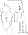
図1に示されている回路装置10はまず、特に力率補正に使用される前調整器12を有している。前調整器12には4つのスイッチを備えた完全ブリッジ構造が続く。これは整流子として機能し、フィルタ回路18を介してランプ16に供給される電圧信号の極性を変化させる。制御回路20は、入力信号としてランプ電流ILとランプ電圧ULを受け取り、出力信号として、完全ブリッジ14のスイッチに対する駆動回路22に供給される制御信号z(t)を形成する。制御回路(20)は一般的に出力調整素子を有しており、出力調整素子がPWM(パルス幅変調)モジュールを制御するための信号発生器を駆動する。制御回路はアナログ式にも、またマイクロプロセッサを用いてデジタル式にも実現することできる。以下では、例として、最後に挙げた実施形態を説明する。制御回路20の内部には、マイクロプロセッサ24、信号発生器26、及びPWMモジュール28が配置されている。図2aを参照すれば、従来技術では一方でPWMモジュール28の変調入力側に信号
The

完全ブリッジ回路及び制御回路14,20の全体は高スイッチング周波数向けに設計されていなければならない。これは結果として、一方では必要な構成素子のための高コストを、さらには高いスイッチング損を生じる。他方では、PWMモジュール28に対して完全な信号シグナチャを供給しなければならない(古典的なクラスD原理に比較されうる)という高い要求が信号発生器26に課せられる。
The complete bridge and
特許文献1の第7頁第31〜32行に察知されるように、PWMモジュール28に供給される電圧信号x(t)は、ランプ16を制御するために要望される波形の低電圧版である。言い換えれば、全情報が信号x(t)に込められている。
The voltage signal x (t) supplied to the
まとめると、結論としては、上で言及した特許文献4による元の定式化に比べればたしかに或る程度の進歩が為されているものの、許容できる価格の大量生産品として使用することを可能にするのには十分ではない。
本発明の課題は、所望の結果、すなわち、放電ランプ内で金属添加物の可能な限り広範囲の混合が低コストで実現されるように、冒頭で述べた回路装置を発展させることである。 The object of the present invention is to develop the circuit arrangement described at the outset in such a way that the desired result, i.e. the widest possible mixing of the metal additives in the discharge lamp, is achieved at low cost.
上記課題は、少なくとも1つの高圧放電ランプを作動させるための回路装置であって、完全ブリッジ構造の4つのスイッチを有しており、ただし、第1及び第2のスイッチは第1の半ブリッジ分岐を、第3及び第4のスイッチは第2の半ブリッジ分岐を形成しており、さらに、前記高圧放電ランプを前記第1及び第2の半ブリッジ分岐の中心の間に結合するための少なくとも2つの端子と、回路装置に直流電圧信号を供給するための少なくとも2つの端子と、前記4つのスイッチを制御するための制御回路とを有する形式の回路装置において、前記制御回路は、前記4つのスイッチに対する制御信号[数式]を供給するように設計されており、前記制御信号のクロックは第1の周波数と第2の周波数の間で掃引され、前記制御信号のパルス幅及び/又は位相は予め設定可能な第3の周波数により変調されるようにすることにより解決される。 The object is a circuit arrangement for operating at least one high-pressure discharge lamp, comprising four switches of a complete bridge structure, wherein the first and second switches are first half-bridge branches. The third and fourth switches form a second half-bridge branch, and at least two for coupling the high-pressure discharge lamp between the centers of the first and second half-bridge branches. In a circuit device of a type having one terminal, at least two terminals for supplying a DC voltage signal to the circuit device, and a control circuit for controlling the four switches, the control circuit includes the four switches. , The control signal clock is swept between a first frequency and a second frequency, the pulse width of the control signal Beauty / or phase is solved by to be modulated by the third frequency that can be set in advance.
本発明は、例えばPWMモジュールの形態のコンパレータに対して、一方では入力信号x(t)として、すなわち変調入力側において、振幅変調信号のみが使用可能であり、他方でシステム入力側には、信号y(t)として、掃引された搬送周波信号が供給されるようにすると、特に有利な実施形態が達成されるという認識に基づいている。同様に、上記課題は、パルス幅の代わりに位相を適切な仕方で変調することによっても解決される。その上、パルス幅変調の深さ又は位相シフトの深さを介して、ランプに対する交流電圧出力側における変調の深さが調整される。それゆえ、有利な実施形態では、走査切換プロセスはおよそ50kHzのオーダーであり、したがって省電流かつ低コストの実施が可能となる。 For example, for the comparator in the form of a PWM module, the invention can use only the amplitude modulation signal on the one hand as the input signal x (t), ie on the modulation input side, and on the other hand the signal on the system input side. It is based on the recognition that a particularly advantageous embodiment is achieved if a swept carrier frequency signal is supplied as y (t). Similarly, the above problem is solved by modulating the phase in an appropriate manner instead of the pulse width. In addition, the modulation depth on the AC voltage output side for the lamp is adjusted via the pulse width modulation depth or the phase shift depth. Therefore, in an advantageous embodiment, the scan switching process is on the order of approximately 50 kHz, thus allowing current saving and low cost implementation.
特に有利な実施形態では、アナログの振幅変調信号x(t)がLC素子においてフィルタリングごとにデジタル方形波信号から形成される。この信号の周波数は50kHzよりも低く、有利には20kHzと35kHzの間である。 In a particularly advantageous embodiment, an analog amplitude modulation signal x (t) is formed from the digital square wave signal for each filtering in the LC element. The frequency of this signal is lower than 50 kHz, preferably between 20 kHz and 35 kHz.
信号y(t)のクロック周波数は好適には150kHzよりも低く、有利には、それによって作動させるべきランプの設計に応じて、40kHzと60kHzの間、又は80kHzと120kHzの間である。掃引周波数は好適には50Hzと500Hzの間、有利には80Hzと200Hzの間である。 The clock frequency of the signal y (t) is preferably below 150 kHz, advantageously between 40 kHz and 60 kHz, or between 80 kHz and 120 kHz, depending on the lamp design to be operated thereby. The sweep frequency is preferably between 50 and 500 Hz, preferably between 80 and 200 Hz.
パルス幅変調の場合には、完全ブリッジ構造の対角線分岐内のスイッチがそれぞれ自らの信号によって制御されるように、制御回路が設計されていると好適である。位相変調の場合には、制御回路は位相シフトモジュールを内蔵しており、この位相シフトモジュールのクロック入力側は第1の周波数と第2の周波数の間で掃引される信号のソースに結合されており、この位相シフトモジュールの変調入力側は第3の周波数(fa)の信号のソースに結合されている。 In the case of pulse width modulation, it is preferable that the control circuit is designed so that each switch in the diagonal branch of the complete bridge structure is controlled by its own signal. In the case of phase modulation, the control circuit incorporates a phase shift module, and the clock input side of this phase shift module is coupled to the source of the signal swept between the first frequency and the second frequency. The modulation input side of the phase shift module is coupled to the source of the signal of the third frequency (f a ).
パルス幅は非対称的又は対称的に変調してよい。好適には、制御回路はPWMモジュールを内蔵しており、このPWMモジュールのクロック入力側は第1の周波数と第2の周波数の間で掃引される信号のソースに結合されており、このPWMモジュールの変調入力側は第3の周波数の信号のソースに結合されている。 The pulse width may be modulated asymmetrically or symmetrically. Preferably, the control circuit includes a PWM module, the clock input side of which is coupled to the source of the signal swept between the first frequency and the second frequency, the PWM module The modulation input side is coupled to the source of the third frequency signal.
有利には、PWMモジュールの変調入力側はさらにオフセット信号のソースにも結合されており、これにより、完全ブリッジ構造における基本出力を制御することができる。それと同時に、ランプ出力の調整のために介入することも可能となる。 Advantageously, the modulation input side of the PWM module is also coupled to the source of the offset signal, so that the basic output in a full bridge structure can be controlled. At the same time, it is possible to intervene to adjust the lamp output.
別の有利な実施形態は従属請求項から把握することができる。 Further advantageous embodiments can be taken from the dependent claims.
図2bには、図1のPWMモジュール28の本発明による制御が示されている。図2a及び2bに示されているのと同じ機能は、クロック入力側において鋸波信号から形成された方形波信号により制御されるPWMモジュールの代わりに、コンパレータを備えた回路によっても実現可能であることに再度注意されたい。つまり、簡略化した表示では、PWMモジュールは、クロック入力側において鋸波信号を受け取り、変調入力側においてパルス幅信号に変換される変調信号を受け取るコンパレータとして理解することができる。そえゆえ以下では、クロック入力側に印加される信号、すなわち、PWMモジュールの入力側における方形波信号又はコンパレータのクロック入力側における鋸波信号は、一般的にy(t)で表される。ここで、クロック入力側には、掃引されたクロック周波数ftと同じ周波数の鋸波信号が印加される。PWMモジュール28の変調入力側には、信号x(t)として、振幅変調情報を含んだ信号、すなわち、信号
FIG. 2b shows the control according to the invention of the
図4では、信号y(t)として、基本発振器信号(曲線a)参照)から導出される対称的なコンパレータランプ信号が形成される。図5では、基本発振器信号から非対称的なコンパレータランプ信号が形成される。 In FIG. 4, a symmetrical comparator ramp signal derived from the basic oscillator signal (see curve a)) is formed as signal y (t). In FIG. 5, an asymmetrical comparator ramp signal is formed from the basic oscillator signal.
図6及び7には、再び、対称的なPWMモジュール出力信号(図6)と非対称的なPWMモジュール出力信号(図7)とによる制御信号z1(t)及びz2(t)の2重対の形成が示されている。ここでは、図4及び5において使用されているのと同じ基本発振器信号から、当業者に周知の手段によって、基本発振器周波数の2倍の周波数を有するコンパレータランプ信号y(t)が導出される。変調入力側に印加されるそれぞれの振幅変調信号x(t)は図4及び5の場合と同じである。この結果、完全ブリッジのスイッチQ1〜Q4を制御するPWMモジュール28(図1では図示せず)の出力信号の2重対z1(t)及びz2(t)が生じる。当業者にとっては明らかなように、互いに対角線上に位置するそれぞれのスイッチ、すなわち、Q1とQ4ないしQ2とQ3は、時間τの間同時に導通している。 6 and 7 again show the double of the control signals z 1 (t) and z 2 (t) by the symmetric PWM module output signal (FIG. 6) and the asymmetric PWM module output signal (FIG. 7). The formation of a pair is shown. Here, a comparator ramp signal y (t) having a frequency twice that of the fundamental oscillator frequency is derived from the same fundamental oscillator signal used in FIGS. 4 and 5 by means well known to those skilled in the art. The respective amplitude modulation signals x (t) applied to the modulation input side are the same as those in FIGS. This results in a double pair z 1 (t) and z 2 (t) of the output signal of the PWM module 28 (not shown in FIG. 1) that controls the switches Q 1 -Q 4 of the full bridge. As will be apparent to those skilled in the art, the respective switches located diagonally to each other, ie Q 1 and Q 4 or Q 2 and Q 3, are conducting simultaneously during time τ.
図4〜7による4つのすべての実施形態において、PWMモジュール28の出力側にはftよりも高い周波数、つまり、55kHzよりも高い周波数を有する方形波信号は現れない。
In all four embodiments according to FIGS. 4-7, a frequency higher than f t on the output side of the
図8には、PWMモジュールの代わりに位相シフトモジュール(図示せず)を用いた位相シフトによるPWMモジュール出力信号の形成が原理的に示されている。ここでは、曲線a)として示された基本発振器信号が、信号z1(t)と曲線c)として示された遅延信号とを形成している。なお、遅延信号の遅延値ΔiはPWM変調信号x(t)に反比例している。したがって、比較的大きな振幅を有するPWM変調信号は小さな遅延につながり、比較的小さな振幅を有するPWM変調信号は大きな遅延につながる。図8において曲線b)で示されている垂直矢印は、図8cに示されているz1(t)とz2(t)との間にある遅延Δ1,Δ2等に対応している。 FIG. 8 shows in principle the formation of a PWM module output signal by phase shift using a phase shift module (not shown) instead of the PWM module. Here, the basic oscillator signal shown as curve a) forms the signal z 1 (t) and the delayed signal shown as curve c). The delay value delta i of the delay signal is inversely proportional to the PWM modulation signal x (t). Therefore, a PWM modulated signal having a relatively large amplitude leads to a small delay, and a PWM modulated signal having a relatively small amplitude leads to a large delay. 8 corresponds to the delays Δ 1 , Δ 2, etc. between z 1 (t) and z 2 (t) shown in FIG. 8c. .
一般的に言えば、対称的な信号y(t)を用いたPWMモジュール28の出力信号の形成方法が選好される。といのも、この方法では、完全ブリッジ14の出力側に発生する高調波が比較的小さいからである。
Generally speaking, the method of forming the output signal of the
10 回路装置
12 前調整器
14 完全ブリッジ構造
16 高圧放電ランプ
18 フィルタ回路
20 制御回路
22 駆動回路
22a 駆動回路
22b 駆動回路
24 マイクロプロセッサ
26 信号発生器
28 PWMモジュール
30 方形波発生器
32 LCフィルタ
34 減衰素子
38 オフセット信号ソース
40 加算器
DESCRIPTION OF
Claims (9)
完全ブリッジ構造の4つのスイッチ(Q1〜Q4)を有しており、ただし、第1及び第2のスイッチ(Q1,Q2)は第1の半ブリッジ分岐を、第3及び第4のスイッチ(Q3,Q4)は第2の半ブリッジ分岐を形成しており、
さらに、前記高圧放電ランプ(16)を前記第1及び第2の半ブリッジ分岐の中心の間に結合するための少なくとも2つの端子と、
回路装置(10)に直流電圧信号を供給するための少なくとも2つの端子と、
前記4つのスイッチ(Q1〜Q4)を制御するための制御回路(20)とを有する形式の回路装置において、
前記制御回路(20)は、前記4つのスイッチ(Q1〜Q4)に対する制御信号
前記制御回路(20)はPWMモジュール(28)を有しており、該PWMモジュールのクロック入力側は前記第1及び第2の周波数の間で掃引されるクロックのソースに、前記PWMモジュールの変調入力側は前記第3の周波数(f a )の信号のソースに結合されていることを特徴とする、少なくとも1つの高圧放電ランプ(16)を作動させるための回路装置。 A circuit arrangement for operating at least one high-pressure discharge lamp (16),
It has four switches (Q 1 to Q 4 ) of a complete bridge structure, except that the first and second switches (Q 1 , Q 2 ) have a first half-bridge branch, a third and a fourth switch. Switches (Q 3 , Q 4 ) form a second half-bridge branch,
And at least two terminals for coupling the high pressure discharge lamp (16) between the centers of the first and second half-bridge branches;
At least two terminals for supplying a DC voltage signal to the circuit arrangement (10);
In the circuit device of the type having a control circuit and (20) for controlling the four switches (Q 1 to Q 4),
Said control circuit (20), said four control signals for the switches (Q 1 to Q 4)
The control circuit (20) has a PWM module (28), and the clock input side of the PWM module is used as a source of a clock swept between the first and second frequencies. Circuit arrangement for operating at least one high-pressure discharge lamp (16), characterized in that the input side is coupled to the source of the signal of the third frequency (f a ) .
Applications Claiming Priority (1)
| Application Number | Priority Date | Filing Date | Title |
|---|---|---|---|
| DE10333820A DE10333820A1 (en) | 2003-07-24 | 2003-07-24 | Circuit arrangement for operating at least one high-pressure discharge lamp |
Publications (2)
| Publication Number | Publication Date |
|---|---|
| JP2005044812A JP2005044812A (en) | 2005-02-17 |
| JP4638698B2 true JP4638698B2 (en) | 2011-02-23 |
Family
ID=33483057
Family Applications (1)
| Application Number | Title | Priority Date | Filing Date |
|---|---|---|---|
| JP2004217819A Expired - Fee Related JP4638698B2 (en) | 2003-07-24 | 2004-07-26 | Circuit arrangement for operating at least one high-pressure discharge lamp |
Country Status (8)
| Country | Link |
|---|---|
| US (1) | US8125156B2 (en) |
| EP (1) | EP1501338A3 (en) |
| JP (1) | JP4638698B2 (en) |
| KR (1) | KR20050012150A (en) |
| CN (1) | CN1578579A (en) |
| CA (1) | CA2475400A1 (en) |
| DE (1) | DE10333820A1 (en) |
| TW (1) | TWI270324B (en) |
Families Citing this family (7)
| Publication number | Priority date | Publication date | Assignee | Title |
|---|---|---|---|---|
| DE102004042996A1 (en) | 2004-09-06 | 2006-03-09 | Patent-Treuhand-Gesellschaft für elektrische Glühlampen mbH | Circuit arrangement for operating at least one high-pressure discharge lamp |
| DE102005059762A1 (en) | 2005-12-14 | 2007-06-21 | Patent-Treuhand-Gesellschaft für elektrische Glühlampen mbH | Circuit arrangement and method for operating high-pressure gas discharge lamps |
| CN101563960B (en) | 2007-01-10 | 2013-06-12 | 奥斯兰姆有限公司 | Circuit arrangement and method for operating a high-pressure discharge lamp |
| DE102009016579A1 (en) * | 2009-04-06 | 2010-10-14 | Osram Gesellschaft mit beschränkter Haftung | Circuit arrangement and method for operating a high-pressure discharge lamp |
| JP5053395B2 (en) | 2010-01-29 | 2012-10-17 | Tdkラムダ株式会社 | Discharge lamp lighting device |
| CN103797898A (en) * | 2011-09-14 | 2014-05-14 | 皇家飞利浦有限公司 | Digitally controlled electronic ballast with anti-striation control and method of operation thereof |
| DE102019127709B4 (en) * | 2019-10-15 | 2023-05-04 | Webasto SE | Process and device for PWM control of HV components |
Citations (2)
| Publication number | Priority date | Publication date | Assignee | Title |
|---|---|---|---|---|
| JPH11297482A (en) * | 1998-04-06 | 1999-10-29 | Meiji Natl Ind Co Ltd | Ac high-pressure discharge lamp lighting device |
| JP2003502813A (en) * | 1999-06-17 | 2003-01-21 | コーニンクレッカ フィリップス エレクトロニクス エヌ ヴィ | Elimination of vertical separation in discharge lamps |
Family Cites Families (9)
| Publication number | Priority date | Publication date | Assignee | Title |
|---|---|---|---|---|
| US4904907A (en) * | 1988-02-26 | 1990-02-27 | General Electric Company | Ballast circuit for metal halide lamp |
| CN1156200C (en) | 1995-12-08 | 2004-06-30 | 皇家菲利浦电子有限公司 | Ballast system |
| US5923129A (en) * | 1997-03-14 | 1999-07-13 | Linfinity Microelectronics | Apparatus and method for starting a fluorescent lamp |
| JP3742270B2 (en) * | 2000-02-10 | 2006-02-01 | 株式会社小糸製作所 | Discharge lamp lighting circuit |
| US6400100B1 (en) * | 2000-07-20 | 2002-06-04 | Philips Electronics North America Corporation | System and method for determining the frequency of longitudinal mode required for color mixing in a discharge lamp |
| US6653799B2 (en) | 2000-10-06 | 2003-11-25 | Koninklijke Philips Electronics N.V. | System and method for employing pulse width modulation with a bridge frequency sweep to implement color mixing lamp drive scheme |
| US6680582B1 (en) * | 2000-10-06 | 2004-01-20 | Koninklijke Philips Electronics N.V. | System and method for employing pulse width modulation for reducing vertical segregation in a gas discharge lamp |
| US6483259B1 (en) * | 2001-06-12 | 2002-11-19 | Koninklijke Phillips Electronics N.V. | Method and apparatus for determining power frequencies that cause arc instabilities in discharge lamps |
| US6788007B2 (en) * | 2001-12-21 | 2004-09-07 | Koninklijke Philips Electronics N.V. | Use of arc straightening in HID lamps operated at VHF frequencies |
-
2003
- 2003-07-24 DE DE10333820A patent/DE10333820A1/en not_active Ceased
-
2004
- 2004-07-06 TW TW093120216A patent/TWI270324B/en not_active IP Right Cessation
- 2004-07-06 EP EP04015908A patent/EP1501338A3/en not_active Withdrawn
- 2004-07-12 US US10/888,022 patent/US8125156B2/en not_active Expired - Fee Related
- 2004-07-21 CA CA002475400A patent/CA2475400A1/en not_active Abandoned
- 2004-07-22 KR KR1020040057134A patent/KR20050012150A/en not_active Application Discontinuation
- 2004-07-23 CN CNA2004100545584A patent/CN1578579A/en active Pending
- 2004-07-26 JP JP2004217819A patent/JP4638698B2/en not_active Expired - Fee Related
Patent Citations (2)
| Publication number | Priority date | Publication date | Assignee | Title |
|---|---|---|---|---|
| JPH11297482A (en) * | 1998-04-06 | 1999-10-29 | Meiji Natl Ind Co Ltd | Ac high-pressure discharge lamp lighting device |
| JP2003502813A (en) * | 1999-06-17 | 2003-01-21 | コーニンクレッカ フィリップス エレクトロニクス エヌ ヴィ | Elimination of vertical separation in discharge lamps |
Also Published As
| Publication number | Publication date |
|---|---|
| US8125156B2 (en) | 2012-02-28 |
| EP1501338A3 (en) | 2009-03-04 |
| DE10333820A1 (en) | 2005-02-17 |
| TW200520630A (en) | 2005-06-16 |
| TWI270324B (en) | 2007-01-01 |
| CA2475400A1 (en) | 2005-01-24 |
| KR20050012150A (en) | 2005-01-31 |
| CN1578579A (en) | 2005-02-09 |
| US20050285544A1 (en) | 2005-12-29 |
| JP2005044812A (en) | 2005-02-17 |
| EP1501338A2 (en) | 2005-01-26 |
Similar Documents
| Publication | Publication Date | Title |
|---|---|---|
| JP2002203689A (en) | Driving device and driving method of cold cathode fluorescent tube using piezoelectric transformer | |
| JP4638698B2 (en) | Circuit arrangement for operating at least one high-pressure discharge lamp | |
| US7456816B2 (en) | Lamp frequency control system for display and method for controlling lamp frequency | |
| CN1893760B (en) | Device and method for providing a sinusoidally amplitude modulated operating voltage | |
| KR101073302B1 (en) | Circuit arrangement and method for operating a high-pressure discharge lamp | |
| US7145293B2 (en) | Electronic ballast having resonance excitation for generating a transfer voltage | |
| EP1696547A1 (en) | Discharge lamp operation device and lighting fixture | |
| US6870324B2 (en) | Method for color mixing with arc stability and straightening of HID lamps operated at high frequencies using duty cycle modulation | |
| US8648789B2 (en) | Control device for controlling the output of one or more full-bridges | |
| US6498441B1 (en) | Method for coloring mixing of hid lamps operated at VHF frequencies using duty cycle modulation | |
| JPH0951681A (en) | Wide input piezoelectric transformer inverter | |
| JP2007294448A (en) | Lcd back-light driving circuit | |
| JP2004521463A (en) | Mixed mode controller for ballast circuit | |
| TWI260187B (en) | Lighting system | |
| KR101358173B1 (en) | Circuit arrangement, and method for the operation of a high-pressure discharge lamp | |
| JP4305160B2 (en) | Discharge lamp lighting device | |
| KR100395094B1 (en) | Asynchronous driving circuit of back-light inverter for lcd panel | |
| JP2000268986A (en) | Discharge lamp lighting device | |
| JPS62277077A (en) | Dc/ac inverter system | |
| US20090213624A1 (en) | Audio apparatus, switching power supply, and switching control method | |
| JPH0425267A (en) | Ringing signal oscillator | |
| JP2000506000A (en) | Circuit device | |
| JPH076890A (en) | Fluorescent lamp lighting device | |
| JP2003133097A (en) | Lighting device and method for lamp | |
| JPH01115098A (en) | Inverter |
Legal Events
| Date | Code | Title | Description |
|---|---|---|---|
| A621 | Written request for application examination |
Free format text: JAPANESE INTERMEDIATE CODE: A621 Effective date: 20070329 |
|
| A131 | Notification of reasons for refusal |
Free format text: JAPANESE INTERMEDIATE CODE: A131 Effective date: 20091204 |
|
| A601 | Written request for extension of time |
Free format text: JAPANESE INTERMEDIATE CODE: A601 Effective date: 20100301 |
|
| A602 | Written permission of extension of time |
Free format text: JAPANESE INTERMEDIATE CODE: A602 Effective date: 20100304 |
|
| A521 | Written amendment |
Free format text: JAPANESE INTERMEDIATE CODE: A523 Effective date: 20100602 |
|
| TRDD | Decision of grant or rejection written | ||
| A01 | Written decision to grant a patent or to grant a registration (utility model) |
Free format text: JAPANESE INTERMEDIATE CODE: A01 Effective date: 20101112 |
|
| A01 | Written decision to grant a patent or to grant a registration (utility model) |
Free format text: JAPANESE INTERMEDIATE CODE: A01 |
|
| A61 | First payment of annual fees (during grant procedure) |
Free format text: JAPANESE INTERMEDIATE CODE: A61 Effective date: 20101126 |
|
| FPAY | Renewal fee payment (event date is renewal date of database) |
Free format text: PAYMENT UNTIL: 20131203 Year of fee payment: 3 |
|
| R150 | Certificate of patent or registration of utility model |
Free format text: JAPANESE INTERMEDIATE CODE: R150 |
|
| R250 | Receipt of annual fees |
Free format text: JAPANESE INTERMEDIATE CODE: R250 |
|
| R250 | Receipt of annual fees |
Free format text: JAPANESE INTERMEDIATE CODE: R250 |
|
| LAPS | Cancellation because of no payment of annual fees |