JP4635679B2 - Method for manufacturing electromagnetic shielding housing - Google Patents
Method for manufacturing electromagnetic shielding housing Download PDFInfo
- Publication number
- JP4635679B2 JP4635679B2 JP2005093131A JP2005093131A JP4635679B2 JP 4635679 B2 JP4635679 B2 JP 4635679B2 JP 2005093131 A JP2005093131 A JP 2005093131A JP 2005093131 A JP2005093131 A JP 2005093131A JP 4635679 B2 JP4635679 B2 JP 4635679B2
- Authority
- JP
- Japan
- Prior art keywords
- insulating layer
- electromagnetic wave
- wave shielding
- casing
- housing
- Prior art date
- Legal status (The legal status is an assumption and is not a legal conclusion. Google has not performed a legal analysis and makes no representation as to the accuracy of the status listed.)
- Expired - Fee Related
Links
Images

Landscapes
- Shielding Devices Or Components To Electric Or Magnetic Fields (AREA)
- Moulds For Moulding Plastics Or The Like (AREA)
- Injection Moulding Of Plastics Or The Like (AREA)
Description
本発明は、携帯電話機等の電子機器に使用される電磁波シールド筐体の製造方法に関するものである。 The present invention relates to a method for manufacturing an electromagnetic wave shielding casing used in an electronic device such as a mobile phone.
従来より、電子機器の筐体として、電磁波シールド機能を備えた様々な電磁波シールド筐体が提供されている。 Conventionally, various electromagnetic wave shielding cases having an electromagnetic wave shielding function have been provided as cases of electronic devices.
携帯電話等の電子機器では、回路基板を樹脂製の筐体に内装する際、前記筐体の内面に金属膜を形成して電磁波シールドを必要とする回路部品を覆うことが行われている。この金属膜は、メッキ、塗装、蒸着等の表面処理により形成することができる(特許文献1、従来の技術の欄参照)。 In an electronic device such as a mobile phone, when a circuit board is mounted in a resin casing, a metal film is formed on the inner surface of the casing to cover a circuit component that requires an electromagnetic shield. This metal film can be formed by surface treatment such as plating, painting, vapor deposition, etc. (see Patent Document 1, column of conventional technology).
しかし、上記のように金属膜の形成により電磁シールド性を付与する場合には、樹脂成形等により筐体を形成した後に、更に金属膜形成のための処理を行わなければならず、製造工程が煩雑化すると共に製造コストも増大してしまうものであった。 However, when providing electromagnetic shielding properties by forming a metal film as described above, after forming the housing by resin molding or the like, further processing for forming the metal film must be performed, and the manufacturing process This complicates the manufacturing cost.
また、筐体に他の部材に嵌合係止するためにフック状の嵌合係止部等を設ける場合には、部材の嵌合係止時に嵌合係止部に応力がかかることにより、この嵌合係止部に形成されている金属膜が剥がれ落ちて金属粉の粉落ちが発生し、この金属粉により筐体に内装されている回路基板に短絡が発生してしまうおそれもある。また、筐体の内面の回路基板とが近接する場合に前記回路基板が筐体内面の金属膜によりショートサーキットが生じたりするおそれもある。このため、筐体には部分的に金属膜が形成されていない部分を設ける必要があり、そのため金属膜形成時にマスキングを施したり、金属膜形成後にエッチング処理を施したりするなどの処理を行う必要があって、更に製造工程の煩雑化を招いてしまうものである。 In addition, when providing a hook-like fitting locking part or the like for fitting and locking to another member on the housing, stress is applied to the fitting locking part when fitting and locking the member. The metal film formed on the fitting locking portion may be peeled off to cause metal powder to fall off, and the metal powder may cause a short circuit in the circuit board built in the housing. In addition, when the circuit board on the inner surface of the casing is close to the circuit board, the circuit board may cause a short circuit due to the metal film on the inner surface of the casing. For this reason, it is necessary to provide a part where the metal film is not partially formed on the housing, and therefore, it is necessary to perform a process such as masking at the time of forming the metal film or performing an etching process after forming the metal film. Therefore, the manufacturing process is further complicated.
また、金属膜を設けることなく、筐体に導電性を有する部分と導電性を有しない部分とを形成するために、筐体を導電性樹脂と非導電性樹脂との二色成形により形成することも提案されているが(特許文献1参照)、この場合は二種類の樹脂を用意しなければならず、また成形工程も煩雑なものとなってしまうという問題があった。
本発明は上記の点に鑑みて為されたものであり、導電性を有する部分と導電性を有さない部分とを備える電磁波シールド筐体を少ない工程にて容易に形成することができる電磁波シールド筐体の製造方法を提供することを目的とするものである。 The present invention has been made in view of the above, the electromagnetic wave can be easily formed an electromagnetic wave shield casing Ru and a portion having no partial conductive having conductivity with a small step An object of the present invention is to provide a method for manufacturing a shield casing.
本発明に係る電磁波シールド筐体1の製造方法は、導電性フィラーを含有する熱可塑性樹脂組成物を射出成形して製造する電磁波シールド筐体1の製造方法であって、射出成形時の金型面の一部を他の部分よりも高温とすることにより、電磁波シールド筐体1の表層の一部に導電性フィラーを含まない絶縁層2を形成すると共に他の部分では絶縁層を形成しないことを特徴とするものである。これにより、射出成形を行うと同時に導電性フィラーを含まない絶縁層2が電磁波シールド筐体1に一体に形成される。
The manufacturing method of the electromagnetic wave shielding casing 1 according to the present invention is a manufacturing method of the electromagnetic wave shielding casing 1 that is manufactured by injection molding a thermoplastic resin composition containing a conductive filler, and is a mold at the time of injection molding. By forming a part of the surface at a higher temperature than the other part, the
上記電磁波シールド筐体1の製造方法においては、他の部材に嵌合係止する嵌合係止部3を形成すると共に、前記嵌合係止部3の表層に上記絶縁層2を形成すると、他の部材との嵌合係止時に嵌合係止部3が摩滅して粉落ちが発生しても、導電性の粉が生じることがなく、電磁波シールド筐体1が収容する回路基板等にショートサーキットが発生することを防止することができる。
In the method of manufacturing the electromagnetic wave shield casing 1, to form a
また、上記電磁波シールド筐体1の製造方法においては、電磁波シールド筐体における、表面に電気絶縁性を付与する必要がある部位である、回路と近接する箇所の表層に上記絶縁層2を形成すると、電磁波シールド筐体1が収容する基板上の回路や電子部品等に絶縁層4が近接していても、ショートサーキットが発生することを防止することができる。
Moreover, in the manufacturing method of the said electromagnetic wave shielding housing | casing 1, when the said
また、上記のような電磁波シールド筐体1における上記絶縁層2の厚みは0.02〜0.4mmの範囲となるようにすることが好ましい。
The thickness of the
本発明によれば、熱可塑性樹脂組成物を射出成形するだけで、導電性フィラーを含む電磁波シールド筐体の表層の一部に導電性フィラーを含まない絶縁層を形成することができ、導電性を有する部分と導電性を有さない部分とを備える電磁波シールド筐体を少ない工程にて容易に形成することができるものである。 According to the present invention, it is possible to form an insulating layer containing no conductive filler on a part of the surface layer of the electromagnetic wave shielding housing containing the conductive filler by simply injection molding the thermoplastic resin composition. It is possible to easily form an electromagnetic wave shielding housing having a portion having a portion and a portion having no conductivity with few steps.
以下、本発明を実施するための最良の形態について説明する。 Hereinafter, the best mode for carrying out the present invention will be described.
本発明に係る電磁波シールド筐体1は、導電性フィラーを含む熱可塑性樹脂組成物を射出成形金型5にて射出成形することにより得られる。
The electromagnetic wave shielding housing 1 according to the present invention is obtained by injection molding a thermoplastic resin composition containing a conductive filler with an
熱可塑性樹脂組成物としては、適宜のものが用いられるが、例えばABS樹脂等の熱可塑性樹脂と、ニッケルをコーティングしたカーボンファイバー等のような導電性フィラーとを含有するものを用いることができる。熱可塑性樹脂組成物中の導電性フィラーの含有量は適宜調整されるが、20〜50質量%の範囲とすることが好ましい。熱可塑性樹脂や導電性フィラーの種類は前記のものに限られず、適宜のものを用いることができる。 As the thermoplastic resin composition, an appropriate one can be used, and for example, a composition containing a thermoplastic resin such as an ABS resin and a conductive filler such as carbon fiber coated with nickel can be used. Although content of the electroconductive filler in a thermoplastic resin composition is adjusted suitably, it is preferable to set it as the range of 20-50 mass%. The types of the thermoplastic resin and the conductive filler are not limited to those described above, and appropriate ones can be used.
一方、射出成形金型5としては、図2に示すように、電磁波シールド筐体1と同一形状の空間(キャビティ6)が内部に形成されるものが用いられるが、射出成形時に前記キャビティ6の内面(金型面)を、その一部(以下、高温部7という)が他の部分(以下、低温部8)よりも高い温度に保持することができるものが用いられる。
On the other hand, as the
例えば、上記射出成形金型5の内部に導電性部材からなる棒状のヒータ9を導入配置して通電加熱により金型面を加熱することができるようにすると共に、前記ヒータ9の配置密度を上記高温部7の近傍で部分的に高くしたり、高温部7においてヒータ9の配置位置を金型面に近接させて配置させたり、射出成形金型5の内部にヒータ9を高温部7の近傍にのみ配置したりすることにより、金型面の一部を他の部分よりも高い温度に保持することができるようにするものである。
For example, a rod-
射出成形により電磁波シールド筐体1を製造するにあたっては、上記のような熱可塑性樹脂組成物及び射出成形金型5を用い、例えば射出圧力を60〜150MPa、保圧を30〜60MPa、シリンダー温度をノズル先端で240〜290℃とする条件で射出成形を行うようにする。このとき、上記のように金型面の高温部7を低温部8よりも高い温度に保持するものであり、例えば高温部7の温度を80〜120℃、好ましくは90〜110℃に保持し、低温部8の温度を50〜70℃に保持するものである。
In manufacturing the electromagnetic wave shielding casing 1 by injection molding, the thermoplastic resin composition and the
このようにして熱可塑性樹脂組成物の射出成形を行うと、射出成形金型5に熱硬化性樹脂組成物が射出されて金型面に沿ってスキン層が形成される際に、金型面の高温部7では、熱可塑性樹脂組成物の硬化は低温部8よりもゆっくりと進み、この間、熱可塑性樹脂組成物中の樹脂成分は流動により金型面と導電性フィラーとの間に入り込み、前記金型面と密着した状態で硬化されることとなる。このため、金型面の高温部7では、形成される電磁波シールド筐体1の表面には導電性フィラーが表出せず、またその表層には導電性フィラーが含まれない絶縁層2が形成されることとなる。一方、金型面の低温部8では熱可塑性樹脂組成物が速やかに硬化するため、前記のような樹脂成分の流動は生じず、このため前記のような絶縁層2は形成されないものである。
When injection molding of the thermoplastic resin composition is performed in this manner, the mold surface is formed when the thermosetting resin composition is injected into the
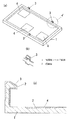
図1はこのような射出成形により形成される電磁波シールド筐体1の一例を示す。図示の電磁波シールド筐体1には、他の部材に嵌合係止する嵌合係止部3が設けられている。図示の嵌合係止部3は、電磁波シールド筐体1の内面側の外縁部から突出するように設けられており、その先端は内側に突出するフック状に形成されている。嵌合係止部3の形状はこのようなものに限られず、他の部材に嵌合係止可能なものであれば良い。この嵌合係止部3は、例えば携帯電話等の電子機器の筐体を構成する他の部材に嵌合係止するために形成されている。
FIG. 1 shows an example of an electromagnetic wave shielding casing 1 formed by such injection molding. The illustrated electromagnetic shielding housing 1 is provided with a
電磁波シールド筐体1における上記絶縁層2は、上記の嵌合係止部3に形成することができる。この場合、嵌合係止部3を他の部材と嵌合させる際に、嵌合係止部3に応力がかかったり他の部材と擦れ合ったりすることにより摩滅してその表面から樹脂粉の粉落ちが生じても、嵌合係止部3の表層には導電性フィラーが含まれていないため、前記樹脂粉中には導電性フィラーは含まれなくなる。従って、電磁波シールド筐体1にて高周波回路等を覆う場合に、上記粉落ちにより生じた樹脂粉が前記回路等に接触しても、ショートサーキット等の不良が発生することがなくなるものである。
The
また、電磁波シールド筐体1における、表面に電気絶縁性を付与する必要のある部位(以下、絶縁部4という)に、上記絶縁層2を形成しても良い。このような絶縁部4としては、例えば電磁波シールド筐体1により高周波回路を覆う場合に回路と近接する箇所が挙げられるものであり、このような絶縁部4に絶縁層2を形成すると、回路やこの回路に実装されている部品と絶縁部4とが接触したとしても、ショートサーキット等の不良が発生することを防止することができるものである。
In addition, the
また、このように形成される電磁波シールド筐体1は、部分的に表層に導電性フィラーを含まない絶縁層2が形成されていることを除いて、導電性フィラーを含有しているものであるから、電磁波シールド筐体1の全体に亘って高い電磁波シールド性を有するものであり、このため、携帯電話機等の電子機器の内部に収容されている高周波回路等に基づく不要な電波の漏洩や電波干渉を防止することができるものである。
Moreover, the electromagnetic wave shielding housing 1 formed in this way contains a conductive filler except that the
また、熱可塑性樹脂組成物の射出成形を行うだけで、他の部材を追加することなく、電磁波シールド筐体1の表層に部分的に絶縁層2を形成することができ、かかる構成の電磁波シールド筐体1を少ない工程で容易に製造すると共に部品点数を削減することができるものである。
Further, the
また、絶縁層2を形成している箇所以外では、電磁波シールド筐体1の外面には導電性が付与されていることから、他の部品を追加しなくても、容易にアースを取ることができるものであり、部品点数を必要最小限に抑えることができるものである。例えば、携帯電話機の場合には、電磁波シールド筐体1に手が触れることによって、人体を通じてアースを取ることができるものである。その結果、帯電による電気的なトラブル、例えばノイズ等の不具合の発生を防止することができるものである。
Further, since the outer surface of the electromagnetic wave shielding casing 1 is provided with conductivity except at the portion where the
上記のような電磁波シールド筐体1は、十分な強度と電磁波シールド性を得るためにはその厚みが0.2〜2.0mmの範囲となるように形成することが好ましい。また、この電磁波シールド筐体1における、絶縁層2の厚みは好ましくは0.02〜0.4mm、更に好ましくは0.02〜0.2mmの範囲となるようにするものであり、このような範囲とすることで良好なシールド効果が得られる。この絶縁層2の厚みは、熱可塑性樹脂組成物の組成に応じ、上記高温部7の温度を変更するなどして調整することができる。
The electromagnetic shielding casing 1 as described above is preferably formed so that its thickness is in the range of 0.2 to 2.0 mm in order to obtain sufficient strength and electromagnetic shielding properties. Moreover, the thickness of the insulating
(実施例)
熱可塑性樹脂組成物として、ニッケルをコーティングしたカーボンファイバーが25質量%添加されたアクリロニトリル・ブタジエン・スチレン樹脂(松下電工株式会社製「ABS(NiCF25%)」)を用い、射出成形により図1に示すような厚み0.3〜0.5mmの電磁波シールド筐体1を形成した。射出成形条件は、射出圧力を130MPa、保圧を45MPa、シリンダー温度をノズル先端で270℃とし、射出成形金型5の金型温度は低温部8を50℃、高温部7を90℃とした。
(Example)
As a thermoplastic resin composition, an acrylonitrile-butadiene-styrene resin (“ABS (NiCF25%)” manufactured by Matsushita Electric Works Ltd.) to which 25% by mass of nickel-coated carbon fiber is added is shown in FIG. 1 by injection molding. An electromagnetic wave shielding casing 1 having a thickness of 0.3 to 0.5 mm was formed. The injection molding conditions were an injection pressure of 130 MPa, a holding pressure of 45 MPa, a cylinder temperature of 270 ° C. at the nozzle tip, and the mold temperature of the
得られた電磁波シールド筐体1を切断して切断面を観察したところ、低温部8に相当する箇所では表層には導電性フィラーを含まない絶縁層2は形成されなかったが、高温部7に相当する箇所では0.04mmの厚みを有する絶縁層2が形成されていた。
When the obtained electromagnetic shielding casing 1 was cut and the cut surface was observed, the insulating
(比較例)
射出成形時に金型温度を全体に亘って50℃とした以外は上記実施例と同様にして電磁波シールド筐体1を形成した。
(Comparative example)
The electromagnetic wave shielding casing 1 was formed in the same manner as in the above example except that the mold temperature was 50 ° C. throughout the injection molding.
得られた電磁波シールド筐体1を切断して切断面を観察したところ、導電性フィラーを含まない絶縁層2は形成されないことが確認された。
When the obtained electromagnetic shielding casing 1 was cut and the cut surface was observed, it was confirmed that the insulating
1 電磁波シールド筐体
2 絶縁層
3 嵌合係止部
4 絶縁部
DESCRIPTION OF SYMBOLS 1 Electromagnetic
Claims (2)
Priority Applications (1)
| Application Number | Priority Date | Filing Date | Title |
|---|---|---|---|
| JP2005093131A JP4635679B2 (en) | 2005-03-28 | 2005-03-28 | Method for manufacturing electromagnetic shielding housing |
Applications Claiming Priority (1)
| Application Number | Priority Date | Filing Date | Title |
|---|---|---|---|
| JP2005093131A JP4635679B2 (en) | 2005-03-28 | 2005-03-28 | Method for manufacturing electromagnetic shielding housing |
Publications (2)
| Publication Number | Publication Date |
|---|---|
| JP2006278568A JP2006278568A (en) | 2006-10-12 |
| JP4635679B2 true JP4635679B2 (en) | 2011-02-23 |
Family
ID=37213034
Family Applications (1)
| Application Number | Title | Priority Date | Filing Date |
|---|---|---|---|
| JP2005093131A Expired - Fee Related JP4635679B2 (en) | 2005-03-28 | 2005-03-28 | Method for manufacturing electromagnetic shielding housing |
Country Status (1)
| Country | Link |
|---|---|
| JP (1) | JP4635679B2 (en) |
Families Citing this family (4)
| Publication number | Priority date | Publication date | Assignee | Title |
|---|---|---|---|---|
| JP5525780B2 (en) * | 2009-08-07 | 2014-06-18 | オリンパスメディカルシステムズ株式会社 | Electronic endoscope device |
| US9655419B2 (en) | 2010-09-07 | 2017-05-23 | Michael J. Nash | Data signal blocking personal communication device holder |
| US10104818B2 (en) * | 2010-09-07 | 2018-10-16 | Caged Idea's Llc | Data transmission blocking holder |
| US20180295262A1 (en) * | 2017-04-06 | 2018-10-11 | Ford Global Technologies, Llc | Conductive emi-shield housings for vehicle cameras |
Family Cites Families (11)
| Publication number | Priority date | Publication date | Assignee | Title |
|---|---|---|---|---|
| JPS6224698A (en) * | 1985-07-24 | 1987-02-02 | 松下電器産業株式会社 | Box body |
| JPS62139400A (en) * | 1985-12-13 | 1987-06-23 | 旭化成株式会社 | Molded unit with electromagnetic shielding properties |
| JPS62256615A (en) * | 1986-04-30 | 1987-11-09 | Mazda Motor Corp | Reaction injection molding device |
| JPS62276896A (en) * | 1986-05-23 | 1987-12-01 | 日立化成工業株式会社 | Molded unit for electromagnetic shielding and manufacture ofthe same |
| JPH07221480A (en) * | 1994-01-31 | 1995-08-18 | Oki Electric Ind Co Ltd | Casing for electronic equipment shielded from electromagnetic waves, and its manufacture |
| JP2000280281A (en) * | 1999-03-30 | 2000-10-10 | Asahi Chem Ind Co Ltd | Insert injection molding method |
| JP2002155471A (en) * | 2000-11-16 | 2002-05-31 | Toray Ind Inc | Carbon fiber and resin composition, molding material and molded article using the same |
| JP2003062852A (en) * | 2001-08-23 | 2003-03-05 | Yoshio Yamada | Injection molding method and apparatus for resin molded article containing metal and/or alloy powder as filler |
| JP3751280B2 (en) * | 2002-12-16 | 2006-03-01 | 北川工業株式会社 | Conductive heat conductive sheet |
| JP2004207661A (en) * | 2002-12-26 | 2004-07-22 | Sony Corp | Heat dissipation member and electronic device having heat dissipation member |
| JP2005051129A (en) * | 2003-07-30 | 2005-02-24 | Sony Corp | Electronics |
-
2005
- 2005-03-28 JP JP2005093131A patent/JP4635679B2/en not_active Expired - Fee Related
Also Published As
| Publication number | Publication date |
|---|---|
| JP2006278568A (en) | 2006-10-12 |
Similar Documents
| Publication | Publication Date | Title |
|---|---|---|
| EP0976311B1 (en) | A shielding housing and a method of producing a shielding housing | |
| US5847317A (en) | Plated rubber gasket for RF shielding | |
| JP2010206792A (en) | Antenna-embedded case for mobile communication terminal and method of manufacturing the same, and mobile communication terminal | |
| JP4635679B2 (en) | Method for manufacturing electromagnetic shielding housing | |
| JPH08148872A (en) | Plastic shield case body | |
| CN104934690A (en) | Method of preparing antenna connection structure, antenna connection structure and mobile communication terminal | |
| TWI532246B (en) | Method for forming a circuit on a housing by spraying or laser engraving | |
| EP4011593A1 (en) | In-mold electronic structure using plating process and method therefor | |
| KR101608357B1 (en) | High voltage connector | |
| KR101318723B1 (en) | Method of forming a metal pattern used for an antenna | |
| KR101387618B1 (en) | Insert antenna module and fabrication method for the same | |
| JP3630595B2 (en) | Electromagnetic wave shield molding | |
| KR100656858B1 (en) | Electromagnetic shielding case and its manufacturing method | |
| US20070289857A1 (en) | Antistatic component and method of manufacturing the same | |
| JPH11274793A (en) | Electromagnetic wave shielding packing and production thereof | |
| CN104704677A (en) | Structure and radio communication device | |
| JP2004136878A (en) | Air venting device | |
| US6682674B2 (en) | Method of making a shield can | |
| US20090277676A1 (en) | In-mold decoration device and manufacturing method thereof | |
| JP2006210526A (en) | Electromagnetic shielding case | |
| JP2010041625A (en) | Onboard waterproof antenna apparatus and waterproof molding method thereof | |
| JP2013070487A (en) | Housing of ecu | |
| GB2349598A (en) | Moulded electrical components | |
| KR200420718Y1 (en) | Electronic Case for Electromagnetic Shielding | |
| JPH1051171A (en) | Electronic equipment housing |
Legal Events
| Date | Code | Title | Description |
|---|---|---|---|
| A621 | Written request for application examination |
Free format text: JAPANESE INTERMEDIATE CODE: A621 Effective date: 20070223 |
|
| A977 | Report on retrieval |
Free format text: JAPANESE INTERMEDIATE CODE: A971007 Effective date: 20090619 |
|
| A131 | Notification of reasons for refusal |
Free format text: JAPANESE INTERMEDIATE CODE: A131 Effective date: 20090623 |
|
| A521 | Request for written amendment filed |
Free format text: JAPANESE INTERMEDIATE CODE: A523 Effective date: 20090824 |
|
| A131 | Notification of reasons for refusal |
Free format text: JAPANESE INTERMEDIATE CODE: A131 Effective date: 20100223 |
|
| A521 | Request for written amendment filed |
Free format text: JAPANESE INTERMEDIATE CODE: A523 Effective date: 20100426 |
|
| TRDD | Decision of grant or rejection written | ||
| A01 | Written decision to grant a patent or to grant a registration (utility model) |
Free format text: JAPANESE INTERMEDIATE CODE: A01 Effective date: 20101026 |
|
| A01 | Written decision to grant a patent or to grant a registration (utility model) |
Free format text: JAPANESE INTERMEDIATE CODE: A01 |
|
| A61 | First payment of annual fees (during grant procedure) |
Free format text: JAPANESE INTERMEDIATE CODE: A61 Effective date: 20101108 |
|
| FPAY | Renewal fee payment (event date is renewal date of database) |
Free format text: PAYMENT UNTIL: 20131203 Year of fee payment: 3 |
|
| FPAY | Renewal fee payment (event date is renewal date of database) |
Free format text: PAYMENT UNTIL: 20131203 Year of fee payment: 3 |
|
| LAPS | Cancellation because of no payment of annual fees |