JP4635334B2 - Switching power supply device and overcurrent detection method - Google Patents
Switching power supply device and overcurrent detection method Download PDFInfo
- Publication number
- JP4635334B2 JP4635334B2 JP2000386940A JP2000386940A JP4635334B2 JP 4635334 B2 JP4635334 B2 JP 4635334B2 JP 2000386940 A JP2000386940 A JP 2000386940A JP 2000386940 A JP2000386940 A JP 2000386940A JP 4635334 B2 JP4635334 B2 JP 4635334B2
- Authority
- JP
- Japan
- Prior art keywords
- switching
- power supply
- overcurrent detection
- waveform
- switching element
- Prior art date
- Legal status (The legal status is an assumption and is not a legal conclusion. Google has not performed a legal analysis and makes no representation as to the accuracy of the status listed.)
- Expired - Fee Related
Links
Images


Landscapes
- Dc-Dc Converters (AREA)
Description
【0001】
【発明の属する技術分野】
本発明は、スイッチング電源装置のスイッチングトランス1次側の過電流検出回路に関し、特に1次側の直流電源電圧が変化した場合においても、一定の負荷電力または所望の負荷電力で過電流検出を行うことができるスイッチング電源装置とこの過電流検出方法に関するものである。
【0002】
【従来の技術】
以下に従来のスイッチング電源装置について、図4,図5を用いて説明する。
【0003】
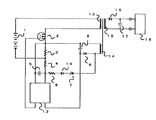
図4は、従来のスイッチング電源の回路を示したものである。図4において、1は入力電力を供給する直流電源、2はスイッチング素子、3は電流検出抵抗、4は抵抗、5はコンデンサ、8は平滑コンデンサ、9はダイオード、12はスイッチング制御用IC、13はスイッチングトランスの1次側巻線、14はスイッチングトランスの1次側補助巻線、15はスイッチングトランスの2次側巻線、16は2次側整流ダイオード、17は2次側平滑コンデンサ、18は出力負荷である。
【0004】
スイッチングトランス1次側のスイッチング素子等の部品における定格オーバーによる破壊防止のため、或いは2次側に伝達させる負荷電力をコントロールするために、スイッチング素子2に流れる電流をスイッチング素子2と直列に接続された電流検出抵抗3をスイッチング制御用IC12の過電流検出端子に接続して過電流の監視を行っている。
【0005】
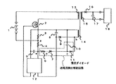
また図5は、図4に示す回路を改善したもので直流電源1の電圧が変化した場合においても、一定の負荷電力で過電流検出を行うことを目的とし、図5の抵抗6,ツェナーダイオード7,コンデンサ10,ダイオード11から成る過電流検出補助回路を追加したものである。
【0006】
スイッチング素子2に直列に接続される電流検出抵抗3の両端に発生する波形に、スイッチングトランスの1次側補助巻線14より発生する波形をコンデンサ10、ダイオード11によってマイナス整流し、ツェナーダイオード7によってクランプした電圧をバイアス電圧として加え、スイッチング制御用IC12の過電流検出端子に接続したものである。
【0007】
【発明が解決しようとする課題】
しかしながら、このような構成の図4に示すスイッチング電源装置は、直流電源の電圧が著しく変化した場合、例えば、直流電源の前段に交流電源を直流電源に整流させる整流回路を備えたAC−DCコンバーターのように交流電源の電圧が100Vから200V以上まで変化した時に、スイッチング素子に流れる電流のみで1次側過電流検出を行った場合には電源電圧変化により、スイッチング素子に流れる電流も変化してしまうため、一定の負荷電力で制御することができないという問題がある。
【0008】
また、前述した図5のスイッチング電源装置は、直流電源の電圧が変化した場合においても、一定の負荷電力で、過電流検出を行うことを目的とし、過電流検出補助回路を追加したものであるが、図5のc点における図6にその波形を示すように、直流電源1の電圧が上昇してパルス幅が著しく狭くなった場合には、マイナス整流を行った電圧がかなり低レベルとなってしまい、直流電源1の電圧低下時と上昇時とでは、あまり変化が得られず、結果的にe点おいてはバイアス電圧として不足となるため、正確に1次側過電流検出を行うことができないという問題があった。
【0009】
本発明は、前記従来技術の問題を解決することに指向するものであり、スイッチング電源装置の1次側の直流電源電圧が変化した場合に、一定の負荷電力あるいは所望の負荷電力により過電流検出を行うことができるスイッチング電源装置とこの過電流検出方法を提供することを目的とする。
【0010】
【課題を解決するための手段】
この目的を達成するために、本発明に係るスイッチング電源装置とこの過電流検出方法におけるスイッチング電源装置は、スイッチングトランスの1次側巻線と直流電源との間に接続されたスイッチング素子と、スイッチング素子と直流電源との間でスイッチング素子と直列に接続された抵抗と、スイッチングトランスの1次側補助巻線から発生する波形をクランプするツェナーダイオードと、抵抗の両端に発生する波形とツェナーダイオードによりクランプされた波形とを積算して、積算した波形の入力される過電流検出端子を有するスイッチング制御用ICとを備え、直流電源の電圧が変化した場合に、前記スイッチング素子にながれる電流の過電流検出を行うことを特徴とする。
【0012】
また、スイッチング電源装置の過電流検出方法は、スイッチングトランス1次側のスイッチング素子と直流電源との間に直列に接続される抵抗の両端に発生する波形に、スイッチングトランスの1次側補助巻線から発生する波形をツェナーダイオードによってクランプさせた波形を積算し、積算した波形をスイッチング制御用ICの過電流検出端子に入力することにより、1次側の直流電源電圧が変化した場合に、前記スイッチング素子にながれる電流の過電流検出を行うことを特徴とする。
【0013】
前記構成によれば、スイッチング素子と直流電源との間に直列に接続された電流検出抵抗の両端に発生する波形と、1次側補助巻線から発生の波形をツェナーダイオードによってクランプした波形とを積算し、この積算波形をスイッチング制御用ICの過電流検出端子に入力することにより、2次側に伝達させる負荷電力を制御して、一定の負荷電力または所望の負荷電力で過電流検出を設定することができる。
【0014】
【発明の実施の形態】
以下、図面を参照して本発明における実施の形態を詳細に説明する。
【0015】
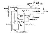
図1は本発明の実施の形態1におけるスイッチング電源装置の回路を示す図である。ここで、前記従来例を示す図5において説明した構成部材に対応し実質的に同等の機能を有するものには同一の符号を付してこれを示す。図1において、1は入力電力を供給する直流電源、2はスイッチング素子、3は電流検出抵抗、4は抵抗、5はコンデンサ、6は抵抗、7はツェナーダイオード、8は平滑コンデンサ、9は整流ダイオード、12はスイッチング制御用IC、13はスイッチングトランスの1次側巻線、14はスイッチングトランスの1次側補助巻線、15はスイッチングトランスの2次側巻線、16は2次側整流ダイオード、17は2次側平滑コンデンサ、18は出力負荷である。なお、図中のスイッチング素子2の記号はMOSFETであるが、他にバイポーラ形トランジスタ、IGBT使用時も同様の図で表す。
【0016】
実施の形態1の動作を説明する。スイッチング制御用IC12より出力される波形をスイッチング素子2に加え、直流電源1から供給された電源はスイッチング素子2により、スイッチングトランスの入力波形として変換される。この入力波形は、1次側巻線13に加えられ、巻線の巻数比に比例した波形が1次側補助巻線14と2次側巻線15に出力される。2次側巻線15より出力された波形は、2次側整流ダイオード16,2次側平滑コンデンサ17により安定な直流に変換され、出力負荷18に供給される。
【0017】
一方、1次側補助巻線14より出力された波形は、整流ダイオード9,平滑コンデンサ8により直流に変換され、スイッチング制御用IC12の電源として供給される。スイッチング素子2と直流電源1に直列に接続された電流検出抵抗3は、スイッチング制御用IC12の過電流検出端子に接続されており、スイッチング素子2に流れるパルス電流を常時監視している。スイッチング制御用IC12の内部には、過電流検出を行う閾値が設定されており、過電流により閾値レベルに達した場合には、スイッチング動作を停止させることにより、スイッチング素子等の部品定格オーバーによる破壊防止、あるいは2次側に伝達させる負荷電力をコントロールしている。
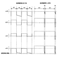
【0018】
図2は、2次側の負荷電力を一定とした場合、図1に示す回路中の各点(a点、b点、d点、e点)の波形を示したものである。a点は電流検出抵抗3の両端の波形、b点は1次側補助巻線14の波形、d点はツェナーダイオード7(カソード側)の波形、e点はスイッチング制御用IC12の過電流検出端子の波形をそれぞれ示したものである。
【0019】
図2に示すa点は、電流検出抵抗3の両端の波形を示したもので、直流電源1の電圧が上昇した場合には、パルス波形の波高値が低下する。b点は、1次側補助巻線14の波形を示したもので、1次側巻線13との巻数比に比例した波高値の波形が、1次側補助巻線14と2次側巻線15に出力される。波形の波高値は図2に示す通り、直流電源1の電圧が上昇した場合に高くなる。
【0020】
また、各点における波形変化のタイミングは、スイッチング素子のOFF→ON→OFFの切り替えに同期しており、スイッチング素子のON期間のみ、電圧がマイナス方向に発生する。この変化を利用し、電流検出抵抗に発生する波形と1次側補助巻線より発生する波形を積算することにより、直流電源の電圧変化による過電流保護動作点変化の補正を行うことができる。
【0021】
具体的には、スイッチング素子2に流れる電流を電流検出抵抗3によって検出を行い、抵抗4を通してスイッチング制御用IC12の過電流検出端子に入力させる。さらに、直流電源1の電圧変化による補正手段として、1次側補助巻線14に発生する波形をツェナーダイオード7によってマイナス側の電圧を適切な波形にクランプさせた後、抵抗6を通した波形をスイッチング制御用IC12の過電流検出端子に加えることにより、この直接クランプした電圧を用いることでパルス幅が短くてもスイッチング制御用IC12の過電流検出閾値のレベルで検出でき、1次側の入力電圧が変化した場合においても、一定の負荷電力または所望の負荷電力で過電流検出を設定することが可能なスイッチング電源を得ることができる。
【0022】
図3は本発明の実施の形態2におけるスイッチング電源装置の回路を示す図である。図3において、1は入力電力を供給する直流電源、2はスイッチング素子、3は電流検出抵抗、4は抵抗、5はコンデンサ、6は抵抗、7はツェナーダイオード、8は平滑コンデンサ、9は整流ダイオード、12はスイッチング制御用IC、13はスイッチングトランスの1次側巻線、14はスイッチングトランスの1次側補助巻線、15はスイッチングトランスの2次側巻線、16は2次側整流ダイオード、17は2次側平滑コンデンサ、18は出力負荷、19はダイオードである。
【0023】
前述の実施の形態1と異なる点は、ダイオード19をツェナーダイオード7と直列に追加した点である。通常、ツェナーダイオードは温度が変化するとツェナー電圧も変化する。したがって、実施の形態1で示す回路では、ツェナーダイオード7によるクランプ電圧が温度変化により影響を受ける。その結果として過電流検出値が温度変化に影響を受けることになる。本実施の形態2においては、この点を改善したもので、ツェナーダイオード7のツェナー電圧温度係数が正の場合において有効である。通常使用されるダイオードは、順電圧温度係数が負である。この点を利用し、ツェナーダイオード7のツェナー電圧温度係数が正に対し、互いに温度変化を打ち消し合うように、ダイオード19に順電圧温度係数が負のものを用いることによりクランプ電圧を温度変化に対して一定にさせることができ、これによって過電流検出値を安定動作させることができる。
【0024】
【発明の効果】
以上説明したように、本発明によれば、スイッチング素子と直流電源との間に直列に接続される抵抗の両端に発生する波形に、スイッチングトランスの1次側補助巻線から発生する波形をツェナーダイオードによってクランプさせた波形を加え、スイッチング制御用ICの過電流検出端子に入力することにより、電源の直流電源電圧が変化した場合においても、スイッチングトランスの2次側に伝達させる負荷電力をコントロールさせ、一定の負荷電力または所望の負荷電力で過電流検出を設定でき、また、1次側スイッチング素子等の部品定格オーバーによる破壊防止、出力過負荷を防ぐ、低コストで安全性と信頼性の高い過電流検出を行う、すぐれたスイッチング電源装置を提供することができるという効果を奏する。
【図面の簡単な説明】
【図1】本発明の実施の形態1におけるスイッチング電源装置の回路を示す図
【図2】本発明の実施の形態1におけるスイッチング電源装置の回路上の信号波形を示す図
【図3】本発明の実施の形態2におけるスイッチング電源装置の回路を示す図
【図4】従来のスイッチング電源装置の回路を示す図
【図5】従来のスイッチング電源装置の別の回路を示す図
【図6】従来のスイッチング電源装置の回路上の信号波形を示す図
【符号の説明】
1 直流電源
2 スイッチング素子
3 電流検出抵抗
4,6 抵抗
5 コンデンサ
7 ツェナーダイオード
8 平滑コンデンサ
9 整流ダイオード
12 スイッチング制御用IC
13 スイッチングトランスの1次側巻線
14 スイッチングトランスの1次側補助巻線
15 スイッチングトランスの2次側巻線
16 2次側整流ダイオード
17 2次側平滑コンデンサ
18 出力負荷
19 ダイオード[0001]
BACKGROUND OF THE INVENTION
The present invention relates to an overcurrent detection circuit on the primary side of a switching transformer of a switching power supply device, and particularly performs overcurrent detection with a constant load power or a desired load power even when the primary side DC power supply voltage changes. The present invention relates to a switching power supply device and an overcurrent detection method that can be used.
[0002]
[Prior art]
Hereinafter, a conventional switching power supply device will be described with reference to FIGS.
[0003]
FIG. 4 shows a conventional switching power supply circuit. In FIG. 4, 1 is a DC power supply for supplying input power, 2 is a switching element, 3 is a current detection resistor, 4 is a resistor, 5 is a capacitor, 8 is a smoothing capacitor, 9 is a diode, 12 is a switching control IC, 13 Is the primary winding of the switching transformer, 14 is the primary auxiliary winding of the switching transformer, 15 is the secondary winding of the switching transformer, 16 is the secondary rectifier diode, 17 is the secondary smoothing capacitor, 18 Is the output load.
[0004]
The current flowing through the
[0005]
FIG. 5 is an improvement of the circuit shown in FIG. 4 and is intended to detect overcurrent with a constant load power even when the voltage of the
[0006]
The waveform generated from the primary side
[0007]
[Problems to be solved by the invention]
However, when the voltage of the DC power supply changes significantly, the switching power supply apparatus shown in FIG. 4 having such a configuration has, for example, an AC-DC converter provided with a rectifier circuit that rectifies the AC power supply to the DC power supply in the previous stage of the DC power supply. When the primary overcurrent detection is performed only with the current flowing through the switching element when the voltage of the AC power supply changes from 100V to 200V or more as shown in FIG. 6, the current flowing through the switching element also changes due to the power supply voltage change. Therefore, there is a problem that control cannot be performed with a constant load power.
[0008]
In addition, the switching power supply device of FIG. 5 described above is provided with an overcurrent detection auxiliary circuit for the purpose of performing overcurrent detection with a constant load power even when the voltage of the DC power supply changes. However, as shown in FIG. 6 at the point c in FIG. 5, when the voltage of the
[0009]
The present invention is directed to solving the problems of the prior art, and when the DC power supply voltage on the primary side of the switching power supply device changes, an overcurrent detection is performed with a constant load power or a desired load power. It is an object of the present invention to provide a switching power supply apparatus capable of performing the above and an overcurrent detection method thereof.
[0010]
[Means for Solving the Problems]
To achieve this object, a switching power supply according to the present invention and a switching power supply in this overcurrent detection method include a switching element connected between a primary winding of a switching transformer and a DC power supply, A resistor connected in series with the switching element between the element and the DC power source, a Zener diode for clamping a waveform generated from the primary side auxiliary winding of the switching transformer, and a waveform generated at both ends of the resistor and the Zener diode And a switching control IC having an overcurrent detection terminal to which the integrated waveform is input, and when the voltage of the DC power source changes, an overcurrent of the current flowing to the switching element The detection is performed.
[0012]
Further, the overcurrent detection method of the switching power supply apparatus is such that the primary auxiliary winding of the switching transformer is formed into a waveform generated at both ends of a resistor connected in series between the switching element on the primary side of the switching transformer and the DC power supply. When the DC power supply voltage on the primary side changes by integrating the waveform obtained by clamping the waveform generated by the zener diode and inputting the integrated waveform to the overcurrent detection terminal of the switching control IC, the switching is performed. An overcurrent detection of a current flowing through the element is performed.
[0013]
According to the above configuration, the waveform generated at both ends of the current detection resistor connected in series between the switching element and the DC power source, and the waveform generated by clamping the waveform generated from the primary side auxiliary winding by the zener diode. By integrating and inputting this integrated waveform to the overcurrent detection terminal of the switching control IC, the load power transmitted to the secondary side is controlled to set overcurrent detection at a constant load power or a desired load power. can do.
[0014]
DETAILED DESCRIPTION OF THE INVENTION
Hereinafter, embodiments of the present invention will be described in detail with reference to the drawings.
[0015]
FIG. 1 is a diagram showing a circuit of a switching power supply apparatus according to
[0016]
The operation of the first embodiment will be described. The waveform output from the switching control IC 12 is added to the
[0017]
On the other hand, the waveform output from the primary side
[0018]
FIG. 2 shows waveforms at points (a point, b point, d point, and e point) in the circuit shown in FIG. 1 when the load power on the secondary side is constant. Point a is the waveform at both ends of the
[0019]
A point a shown in FIG. 2 shows a waveform at both ends of the
[0020]
The timing of waveform change at each point is synchronized with switching of the switching element from OFF → ON → OFF, and the voltage is generated in the negative direction only during the ON period of the switching element. By utilizing this change and integrating the waveform generated in the current detection resistor and the waveform generated from the primary side auxiliary winding, the change in the overcurrent protection operating point due to the voltage change of the DC power supply can be corrected.
[0021]
Specifically, the current flowing through the switching
[0022]
FIG. 3 is a diagram showing a circuit of the switching power supply apparatus according to
[0023]
The difference from the first embodiment is that a diode 19 is added in series with the
[0024]
【The invention's effect】
As described above, according to the present invention, the waveform generated from the primary side auxiliary winding of the switching transformer is changed to the waveform generated at both ends of the resistor connected in series between the switching element and the DC power supply. By adding the waveform clamped by the diode and inputting it to the overcurrent detection terminal of the switching control IC, the load power transmitted to the secondary side of the switching transformer can be controlled even when the DC power supply voltage of the power supply changes. , Overcurrent detection can be set at a constant load power or desired load power, and the primary side switching element etc. can be prevented from being damaged due to overloading of the components, preventing output overload, low cost and high safety and reliability. There is an effect that an excellent switching power supply device that performs overcurrent detection can be provided.
[Brief description of the drawings]
FIG. 1 is a diagram showing a circuit of a switching power supply apparatus according to
DESCRIPTION OF
13 Primary winding of switching
Claims (2)
Priority Applications (1)
| Application Number | Priority Date | Filing Date | Title |
|---|---|---|---|
| JP2000386940A JP4635334B2 (en) | 2000-12-20 | 2000-12-20 | Switching power supply device and overcurrent detection method |
Applications Claiming Priority (1)
| Application Number | Priority Date | Filing Date | Title |
|---|---|---|---|
| JP2000386940A JP4635334B2 (en) | 2000-12-20 | 2000-12-20 | Switching power supply device and overcurrent detection method |
Publications (2)
| Publication Number | Publication Date |
|---|---|
| JP2002191172A JP2002191172A (en) | 2002-07-05 |
| JP4635334B2 true JP4635334B2 (en) | 2011-02-23 |
Family
ID=18853963
Family Applications (1)
| Application Number | Title | Priority Date | Filing Date |
|---|---|---|---|
| JP2000386940A Expired - Fee Related JP4635334B2 (en) | 2000-12-20 | 2000-12-20 | Switching power supply device and overcurrent detection method |
Country Status (1)
| Country | Link |
|---|---|
| JP (1) | JP4635334B2 (en) |
Families Citing this family (1)
| Publication number | Priority date | Publication date | Assignee | Title |
|---|---|---|---|---|
| CN102403697B (en) * | 2011-10-27 | 2016-05-04 | 康佳集团股份有限公司 | A kind of Switching Power Supply over-voltage over-current protection circuit and guard method |
Family Cites Families (3)
| Publication number | Priority date | Publication date | Assignee | Title |
|---|---|---|---|---|
| JPH0628512B2 (en) * | 1987-09-22 | 1994-04-13 | 株式会社村田製作所 | Flyback ringing choke converter |
| JP2777574B2 (en) * | 1988-05-11 | 1998-07-16 | ニチコン株式会社 | Switching power supply |
| JP2504816B2 (en) * | 1988-11-11 | 1996-06-05 | ニチコン株式会社 | Switching power supply |
-
2000
- 2000-12-20 JP JP2000386940A patent/JP4635334B2/en not_active Expired - Fee Related
Also Published As
| Publication number | Publication date |
|---|---|
| JP2002191172A (en) | 2002-07-05 |
Similar Documents
| Publication | Publication Date | Title |
|---|---|---|
| CN107800283B (en) | Active clamp flyback controller and power supply system and control method thereof | |
| TWI475786B (en) | System controller and method for power conversion system | |
| US6125046A (en) | Switching power supply having a high efficiency starting circuit | |
| US7208883B2 (en) | Current detection circuit, and power supply apparatus, power supply system and electronic apparatus using the current detection circuit | |
| US8406023B2 (en) | Discharge loop for power supply circuit and active control circuit thereof | |
| US5349515A (en) | Switch mode power supply with feed-forward pulse limit control | |
| US6381152B1 (en) | Method of driving semiconductor switching device in non-saturated state and power supply apparatus containing such a switching device | |
| JP4379903B2 (en) | Switching power supply | |
| JP3801184B2 (en) | Switching power supply | |
| JP2007068319A (en) | Output voltage detection circuit, isolated switching power supply, and semiconductor device | |
| KR100282327B1 (en) | Switch-Mode Power Supplies with Reduced Input Current Distortion | |
| JPH11252908A (en) | Voltage stabilizer | |
| US10483864B1 (en) | Method for detecting short circuit conditions in frequency control loop components | |
| JP4635334B2 (en) | Switching power supply device and overcurrent detection method | |
| JP7413754B2 (en) | Semiconductor drive equipment and power conversion equipment | |
| JP4983177B2 (en) | Power supply overheat detection circuit | |
| JPH0785648B2 (en) | Switching regulator power supply circuit | |
| JPH02133067A (en) | Switching power supply | |
| JPH05308774A (en) | Power supply | |
| KR100681645B1 (en) | High voltage protection device in SMPS | |
| KR101145551B1 (en) | Synchronous rectifier | |
| JPS5950772A (en) | Power source | |
| KR0121874Y1 (en) | Overvoltage protection circuit | |
| KR0148741B1 (en) | Automatic Overcurrent Detection Circuit | |
| JP3281052B2 (en) | Power circuit |
Legal Events
| Date | Code | Title | Description |
|---|---|---|---|
| A621 | Written request for application examination |
Free format text: JAPANESE INTERMEDIATE CODE: A621 Effective date: 20071213 |
|
| A977 | Report on retrieval |
Free format text: JAPANESE INTERMEDIATE CODE: A971007 Effective date: 20100629 |
|
| A131 | Notification of reasons for refusal |
Free format text: JAPANESE INTERMEDIATE CODE: A131 Effective date: 20100713 |
|
| RD03 | Notification of appointment of power of attorney |
Free format text: JAPANESE INTERMEDIATE CODE: A7423 Effective date: 20100818 |
|
| A521 | Request for written amendment filed |
Free format text: JAPANESE INTERMEDIATE CODE: A523 Effective date: 20100826 |
|
| RD04 | Notification of resignation of power of attorney |
Free format text: JAPANESE INTERMEDIATE CODE: A7424 Effective date: 20100915 |
|
| TRDD | Decision of grant or rejection written | ||
| A01 | Written decision to grant a patent or to grant a registration (utility model) |
Free format text: JAPANESE INTERMEDIATE CODE: A01 Effective date: 20101026 |
|
| A01 | Written decision to grant a patent or to grant a registration (utility model) |
Free format text: JAPANESE INTERMEDIATE CODE: A01 |
|
| A61 | First payment of annual fees (during grant procedure) |
Free format text: JAPANESE INTERMEDIATE CODE: A61 Effective date: 20101108 |
|
| FPAY | Renewal fee payment (event date is renewal date of database) |
Free format text: PAYMENT UNTIL: 20131203 Year of fee payment: 3 |
|
| FPAY | Renewal fee payment (event date is renewal date of database) |
Free format text: PAYMENT UNTIL: 20131203 Year of fee payment: 3 |
|
| S111 | Request for change of ownership or part of ownership |
Free format text: JAPANESE INTERMEDIATE CODE: R313113 |
|
| R350 | Written notification of registration of transfer |
Free format text: JAPANESE INTERMEDIATE CODE: R350 |
|
| S111 | Request for change of ownership or part of ownership |
Free format text: JAPANESE INTERMEDIATE CODE: R313113 |
|
| R350 | Written notification of registration of transfer |
Free format text: JAPANESE INTERMEDIATE CODE: R350 |
|
| S111 | Request for change of ownership or part of ownership |
Free format text: JAPANESE INTERMEDIATE CODE: R313113 |
|
| R350 | Written notification of registration of transfer |
Free format text: JAPANESE INTERMEDIATE CODE: R350 |
|
| LAPS | Cancellation because of no payment of annual fees |