JP4635158B2 - Method for determining surface polarity of polar semiconductors - Google Patents
Method for determining surface polarity of polar semiconductors Download PDFInfo
- Publication number
- JP4635158B2 JP4635158B2 JP2005260379A JP2005260379A JP4635158B2 JP 4635158 B2 JP4635158 B2 JP 4635158B2 JP 2005260379 A JP2005260379 A JP 2005260379A JP 2005260379 A JP2005260379 A JP 2005260379A JP 4635158 B2 JP4635158 B2 JP 4635158B2
- Authority
- JP
- Japan
- Prior art keywords
- single crystal
- plane
- raman
- surface polarity
- sic single
- Prior art date
- Legal status (The legal status is an assumption and is not a legal conclusion. Google has not performed a legal analysis and makes no representation as to the accuracy of the status listed.)
- Expired - Fee Related
Links
Images


Landscapes
- Investigating, Analyzing Materials By Fluorescence Or Luminescence (AREA)
- Testing Or Measuring Of Semiconductors Or The Like (AREA)
- Lasers (AREA)
Description
本発明は、極性を有する半導体の面極性を判定する際に、半導体を破壊することなく半導体の面極性を判定する方法に関するものである。 The present invention relates to a method for determining the surface polarity of a semiconductor without destroying the semiconductor when determining the surface polarity of the semiconductor having polarity.
炭化珪素単結晶(SiC)は、熱的・化学的特性に優れ、禁制帯幅がSi半導体などに比べて大きいなど、電気的特性に優れていることから、高出力、高温、高周波デバイス用半導体材料として注目されている。
SiC単結晶は、化学組成が同じであるが、結晶軸に沿って原子面の配列が異なる結晶多形(ポリタイプ)が数多く存在する。SiC単結晶は、炭素およびシリコンの原子面の積層周期によって、4層周期構造の4H-SiC、6層周期構造の6H-SiC、15層周期の15R-SiCなどに分類される。
Silicon carbide single crystal (SiC) is superior in thermal and chemical properties and has superior electrical characteristics such as a larger forbidden band than Si semiconductors, so it is a semiconductor for high output, high temperature, high frequency devices. It is attracting attention as a material.
SiC single crystals have the same chemical composition, but there are many crystal polymorphs (polytypes) with different arrangement of atomic planes along the crystal axis. SiC single crystals are classified into 4H-SiC with a 4-layer periodic structure, 6H-SiC with a 6-layer periodic structure, 15R-SiC with a 15-layer period, etc., depending on the stacking period of the atomic planes of carbon and silicon.
これらSiC単結晶は極性半導体であり、一方の側の基板表面がSi原子面((0001)面)の場合、反対側の基板表面はC原子面((数1)面)である。なお、以下の記載において、この(数1)面を (000-1)面と表現する。
SiC単結晶の製造を目的とした結晶成長は、原料を加熱昇華させて種結晶から成長させる昇華再結晶法によって行われるのが一般的である。
このとき、種結晶のSi原子面上ではなくC原子面上にSiC単結晶を成長させることでポリタイプを安定的に制御することができ、単一のポリタイプからなる大型SiC単結晶を作製できる(特許文献1参照)。
These SiC single crystals are polar semiconductors. When the substrate surface on one side is a Si atom plane ((0001) plane), the substrate surface on the opposite side is a C atom plane ((Equation 1) plane). In the following description, this (Equation 1) plane is expressed as a (000-1) plane.
Crystal growth for the purpose of producing a SiC single crystal is generally performed by a sublimation recrystallization method in which a raw material is heated and sublimated to grow from a seed crystal.
At this time, the polytype can be stably controlled by growing the SiC single crystal on the C atomic plane instead of the Si atomic plane of the seed crystal, and a large SiC single crystal consisting of a single polytype is produced. Yes (see Patent Document 1).

また、面極性を有するSiC単結晶ウェハを半導体装置として使用する場合、C原子面上に作成した半導体装置の方が、Si原子面上に作成した半導体装置に比べて電子移動速度が大きく電気的特性が優れている(非特許文献1参照)。
SiC単結晶ウェハを取り扱う上では、このように、SiC単結晶の場合は面極性の判別、すなわちSi原子面(Si面)およびC原子面(C面)の判別が必要である。
In addition, when using a SiC single crystal wafer with plane polarity as a semiconductor device, the semiconductor device fabricated on the C atomic plane has a higher electron transfer speed than the semiconductor device fabricated on the Si atomic plane and is electrically Excellent characteristics (see Non-Patent Document 1).
In handling a SiC single crystal wafer, in the case of a SiC single crystal, it is necessary to determine the plane polarity, that is, to determine the Si atomic plane (Si plane) and the C atomic plane (C plane).
SiC単結晶の原子配列を非破壊で決定する方法は可視光を励起光とするラマン散乱の測定により行われるのが一般的である。SiC単結晶では、原子配列の異なる結晶多形に応じて、各結晶多形に固有の振動数・波数にラマン線が得られる。このため、得られたラマン散乱光スペクトルにおいて、ラマン線の振動数・波数を解析することで、該SiC単結晶の結晶多形を比接触、非破壊で簡便に決定することができる(非特許文献2参照)。 The method of nondestructively determining the atomic arrangement of a SiC single crystal is generally performed by measuring Raman scattering using visible light as excitation light. In a SiC single crystal, Raman lines can be obtained at frequencies and wave numbers specific to each crystal polymorph, depending on the crystal polymorphs with different atomic arrangements. For this reason, in the obtained Raman scattered light spectrum, by analyzing the frequency and wave number of the Raman line, the crystal polymorph of the SiC single crystal can be easily determined by specific contact and non-destructive (non-patent) Reference 2).
SiC単結晶の面極性の判別方法の例として、酸化膜形成を利用する方法がある。SiC単結晶は酸素等と反応させることでSiC単結晶基板表面上に酸化膜を形成できる。この時、Si面とC面とでは酸化速度が異なる。
Si面の酸化速度と比較してC面の酸化速度の方が大きいため、同一条件で酸化した場合、Si面に形成される酸化膜と比較してC面に形成される酸化膜の方が厚くなる(非特許文献3参照)。
これを利用し、SiC基板を酸化し、形成された酸化膜の厚みを測定することで、酸化膜の薄い面がSi面、酸化膜の厚い面がC面と判定できる。
As an example of a method for determining the plane polarity of a SiC single crystal, there is a method using oxide film formation. By reacting SiC single crystal with oxygen or the like, an oxide film can be formed on the surface of the SiC single crystal substrate. At this time, the oxidation rate differs between the Si surface and the C surface.
Since the oxidation rate of the C surface is greater than the oxidation rate of the Si surface, when oxidized under the same conditions, the oxide film formed on the C surface compared to the oxide film formed on the Si surface It becomes thicker (see Non-Patent Document 3).
By utilizing this, the SiC substrate is oxidized and the thickness of the formed oxide film is measured, whereby the thin surface of the oxide film can be determined as the Si surface and the thick surface of the oxide film can be determined as the C surface.
SiC単結晶基板の面極性の判別方法として溶融塩と化学反応させる方法がある。SiCは溶融KOH等の溶融塩に溶解する。この時、Si面とC面とで溶融KOHとの反応速度が異なるため、同一条件で溶融KOHと反応させた場合、Si面と比較してC面の方が多く溶解する(非特許文献4参照)。
これを利用し、SiC単結晶基板の両側を溶融KOH等の溶融塩に溶解し、その溶解量を測定することで、溶解量の少ない面がSi面、溶解量の多い面がC面と判定できる。
There is a method of chemically reacting with molten salt as a method of discriminating the plane polarity of a SiC single crystal substrate. SiC dissolves in molten salt such as molten KOH. At this time, since the reaction rate of molten KOH differs between the Si surface and the C surface, the C surface dissolves more than the Si surface when reacted with molten KOH under the same conditions (Non-Patent Document 4). reference).
By using this, both sides of the SiC single crystal substrate are dissolved in molten salt such as molten KOH, and by measuring the amount of dissolution, the surface with the least amount of dissolution is determined to be the Si surface and the surface with the larger amount of dissolution is determined to be the C surface. it can.
また、SiCを溶融KOH等の溶融塩に溶解すると、SiC基板に含まれる結晶欠陥に応じた溶解痕(エッチピット)が生じる。同一条件で溶融KOH等と反応させた場合、Si面とC面とでは溶解痕の形、大きさなどが異なる(非特許文献5参照)。これを利用して、SiC基板の両側を溶融KOH等の溶融塩に溶解し、溶解後の基板表面上の溶解痕を観察することで、Si面およびC面の判定ができる。 Further, when SiC is dissolved in a molten salt such as molten KOH, dissolution marks (etch pits) corresponding to crystal defects included in the SiC substrate are generated. When reacted with molten KOH or the like under the same conditions, the shape and size of dissolution marks differ between the Si surface and the C surface (see Non-Patent Document 5). By utilizing this, both sides of the SiC substrate are dissolved in a molten salt such as molten KOH, and the dissolution surface on the substrate surface after dissolution is observed, whereby the Si surface and the C surface can be determined.
以上に述べた従来技術の酸化膜形成を利用する面極性判別法、および溶融塩との化学反応利用する方法は、いずれもSiC単結晶基板表面上に生じる化学反応および化学反応後の基板を測定することで面極性を判定する破壊検査である。
化学反応のための工程、化学反応後のSiC単結晶基板表面の測定工程など、複数の工程を経て面極性を判定するため、煩雑な手順を必要とする問題点がある。また面極性を判定した後に、再び単結晶SiC基板を利用するためには、SiC単結晶基板表面から酸化膜等の他の物質を除去し、また溶解痕の無い幾何学的に平坦な面を作成するための追加工が必要となる問題点がある。
これら一連の工程に要する時間は数時間から数十時間に及ぶため、面極性判定のために長時間を必要とする問題点がある。
The above-described surface polarity discrimination method using oxide film formation and the method using chemical reaction with molten salt both measure the chemical reaction occurring on the SiC single crystal substrate surface and the substrate after the chemical reaction. This is a destructive inspection to determine the surface polarity.
Since the surface polarity is determined through a plurality of steps such as a step for chemical reaction and a step of measuring the surface of the SiC single crystal substrate after the chemical reaction, there is a problem that requires complicated procedures. In order to use the single crystal SiC substrate again after determining the surface polarity, other materials such as oxide film are removed from the surface of the SiC single crystal substrate, and a geometrically flat surface with no dissolution trace is formed. There is a problem that requires additional work to create.
Since the time required for these series of processes ranges from several hours to several tens of hours, there is a problem that a long time is required for determining the surface polarity.
また、上記非特許文献2に示すような可視光を励起光としたラマン散乱光の測定によるSiC単結晶の原子配列の決定では、ポリタイプの同定は行えるが、特にSiC単結晶のように極性を有する極性半導体の面極性を判定することはできない欠点がある。
本発明は、上記の問題点を解決することを目的とするもので、SiC単結晶等の基板に励起光を照射することで得られるラマン散乱光のスペクトルから極性半導体であるSiC単結晶等の面極性の判定を行う方法を用い、煩雑な手順を必要とせず、追加工又は修正加工の必要性がなく、さらに判定に要する時間を大幅に短縮し、半導体を破壊することなく半導体の面極性を判定する効果的な方法を課題とする。 An object of the present invention is to solve the above-described problems. From a spectrum of Raman scattered light obtained by irradiating a substrate such as a SiC single crystal with excitation light, a SiC single crystal that is a polar semiconductor or the like is obtained. Uses a method for determining the surface polarity, does not require complicated procedures, eliminates the need for additional processing or correction processing, further significantly reduces the time required for determination, and does not destroy the semiconductor An effective method for determining the problem is an issue.
上記の課題に鑑み、次の発明を提供する。
その1)として、極性半導体の面極性を判定する方法において、極性半導体に励起光を照射して得られるラマン散乱光を測定し、測定したラマン散乱光スペクトルから面極性を判定する極性半導体の面極性判定方法を提供する。
その2)として、ラマン散乱光スペクトルの強度から面極性を判定する1)記載の極性半導体の面極性判定方法を提供する。
その3)として、ラマン散乱光スペクトルにおける極性半導体に固有の折り返しモード波数域に存在する複数のラマン線の強度比から面極性を判定する1)記載の極性半導体の面極性判定方法を提供する。
その4)として、励起光として、該極性半導体物質の吸収係数の逆数が400nm以下となる波長を有するレーザー光を用いる1)〜3)のいずれかに記載の極性半導体の面極性判定方法を提供する。
In view of the above problems, the following invention is provided.
As part 1), in the method for determining the surface polarity of a polar semiconductor, the surface of the polar semiconductor is determined by measuring the Raman scattered light obtained by irradiating the polar semiconductor with excitation light and determining the surface polarity from the measured Raman scattered light spectrum. A polarity determination method is provided.
As part 2), the surface polarity determination method for a polar semiconductor according to 1) for determining the surface polarity from the intensity of the Raman scattered light spectrum is provided.
As part 3), there is provided a method for determining the surface polarity of a polar semiconductor according to 1), in which the surface polarity is determined from the intensity ratio of a plurality of Raman lines existing in the folded mode wavenumber region unique to the polar semiconductor in the Raman scattered light spectrum.
As part 4), the surface polarity determination method for a polar semiconductor according to any one of 1) to 3), in which laser light having a wavelength at which the reciprocal of the absorption coefficient of the polar semiconductor material is 400 nm or less is used as excitation light. To do.
本発明は、極性半導体に励起光を照射して得られるラマン散乱光スペクトルを測定することにより、面極性の判定を行い、非破壊かつ非接触で面極性の判定を可能とするという優れた効果を有する。
また、励起光を該単結晶基板の微小領域に集光してラマン散乱光を顕微的に測定することで、極微小領域の面極性の判定を可能とする。さらに、従来技術に比べ、高空間分解能での判定が可能になり、また測定部位を該単結晶基板面上で移動させることにより、容易に単結晶基板全体の面極性分布を測定することが可能となる。
また、ラマン散乱光が比較的強いことからラマン散乱光測定が数分程度で十分であり、短時間で面極性の判定ができるという著しい効果がある。さらに、励起光として短波長のレーザー光を利用することで、該単結晶基板への励起光の侵入長が短くなり、最表面層のからのラマン散乱光の影響を顕在化させることができ、面極性の判定をより明確かつ容易に行えるという効果を有する。
The present invention has an excellent effect of determining a surface polarity by measuring a Raman scattered light spectrum obtained by irradiating a polar semiconductor with excitation light, and enabling nondestructive and non-contact determination of the surface polarity. Have
In addition, it is possible to determine the surface polarity of the extremely minute region by condensing the excitation light on the minute region of the single crystal substrate and microscopically measuring the Raman scattered light. Furthermore, compared with the prior art, it is possible to make a determination with high spatial resolution, and it is possible to easily measure the surface polarity distribution of the entire single crystal substrate by moving the measurement site on the single crystal substrate surface. It becomes.
In addition, since the Raman scattered light is relatively strong, it is sufficient to measure the Raman scattered light for about several minutes, and the surface polarity can be determined in a short time. Furthermore, by using short-wavelength laser light as excitation light, the penetration length of the excitation light into the single crystal substrate is shortened, and the influence of Raman scattered light from the outermost surface layer can be made obvious, There is an effect that the determination of the surface polarity can be performed more clearly and easily.
以下、本発明の特徴を、図に沿って具体的に説明する。なお、以下の説明は、本願発明の理解を容易にするためのものであり、これに制限されるものではない。すなわち、本願発明の技術思想に基づく変形、実施態様、他の例は、本願発明に含まれるものである。 The features of the present invention will be specifically described below with reference to the drawings. In addition, the following description is for making an understanding of this invention easy, and is not restrict | limited to this. That is, modifications, embodiments, and other examples based on the technical idea of the present invention are included in the present invention.
まず、図1のように(0001)面または(000-1)面を持つSiC単結晶基板に励起光を照射して後方散乱測定配置で該SiC単結晶基板からのラマン散乱光スペクトルを計測する。この時、SiC単結晶基板表面は(0001)面または(000-1)面に対して10度まで傾いていた面であってもよい。 First, as shown in FIG. 1, a SiC single crystal substrate having a (0001) plane or a (000-1) plane is irradiated with excitation light, and a Raman scattered light spectrum from the SiC single crystal substrate is measured with a backscattering measurement arrangement. . At this time, the surface of the SiC single crystal substrate may be a surface inclined up to 10 degrees with respect to the (0001) plane or the (000-1) plane.
図2はラマン散乱光スペクトルにより計測できる原子振動を模式的に示したものである。結晶に励起光が照射されると、該結晶の構造に対応して原子が振動する。この振動数は結晶構造により決定され、結晶構造に固有の振動数を示す。結晶表面には原子の振動が表面に局在している表面モードと呼ばれるモードが存在する。 FIG. 2 schematically shows atomic vibrations that can be measured by a Raman scattered light spectrum. When the crystal is irradiated with excitation light, atoms vibrate corresponding to the structure of the crystal. This frequency is determined by the crystal structure, and indicates a frequency unique to the crystal structure. A mode called a surface mode in which atomic vibrations are localized on the surface exists on the crystal surface.
この表面モードの振動数はバルク結晶の振動モードの振動数と異なっていて、振動の振幅は結晶内部に向かって指数関数的に減衰していく定在波である。
またこの表面モードはバルク結晶内を伝播するフォノンモードとは異なり、結晶表面で原子変位の振幅が最大になる。
したがって、最表面層が重いSi原子か軽いC原子かによって振動の振幅が大きくことなるため測定されるラマン散乱光の強度が異なる。
The frequency of the surface mode is different from the frequency of the bulk crystal, and the amplitude of the vibration is a standing wave that attenuates exponentially toward the inside of the crystal.
In addition, unlike the phonon mode propagating in the bulk crystal, this surface mode has the maximum atomic displacement amplitude on the crystal surface.
Therefore, the intensity of the Raman scattered light that is measured differs depending on whether the outermost surface layer is a heavy Si atom or a light C atom.
(0001)面および(000-1)面を有するが裏表のどちらがいずれの面であるかが不明なSiC単結晶基板に対して、該SiC単結晶基板の裏表の両面に励起光を照射し得られるラマン散乱光スペクトルの強度を計測することで、同一振動数・波長における強度を比較し、強度の大きい面が(000-1)面であると判定できる。 A SiC single crystal substrate having a (0001) plane and a (000-1) plane, but which side of the front and back sides is unclear can be irradiated with excitation light on both sides of the SiC single crystal substrate. By measuring the intensity of the Raman scattered light spectrum obtained, it is possible to compare the intensity at the same frequency and wavelength, and determine that the surface with the higher intensity is the (000-1) surface.
また、長周期構造の極性半導体では、折り返しモード域に存在するダブレット(対になったラマン線)も、最表面層が重いSi原子か軽いC原子かによって振動の振幅が大きくことなるため、その強度比が異なる。
(0001)面または(000-1)面を有してはいるが、どちからが不明なSiC単結晶基板に対して、該SiC単結晶基板面に励起光を照射し、折り返しモード域で得られるダブレットの強度を計測することで、該面が(0001)面であるか(000-1)面であるかを判定できる。
In addition, in a polar semiconductor with a long-period structure, the amplitude of vibration also increases depending on whether the outermost surface layer is a heavy Si atom or a light C atom in the doublet (paired Raman line) existing in the folded mode region. The intensity ratio is different.
A SiC single crystal substrate having a (0001) plane or a (000-1) plane but unknown is irradiated with excitation light on the SiC single crystal substrate surface and obtained in a folded mode region. By measuring the strength of the doublet, it can be determined whether the plane is the (0001) plane or the (000-1) plane.
ラマン散乱光スペクトルにより計測では、表面モードとバルク結晶内フォノンモードの計測が同時に行われる。ラマン散乱光を得るために該SiC単結晶基板に照射する励起光は、波長に応じて該SiC単結晶基板内部への侵入長が異なる。長い波長を有する励起光では該SiC単結晶基板内部まで侵入するため、得られるラマン散乱光スペクトルは表面モードと比較してバルク結晶内フォノンモードが相対的に強いスペクトルとなる。 In the measurement by the Raman scattered light spectrum, the surface mode and the phonon mode in the bulk crystal are measured simultaneously. The excitation light applied to the SiC single crystal substrate to obtain Raman scattered light has different penetration lengths into the SiC single crystal substrate depending on the wavelength. Since excitation light having a long wavelength penetrates into the SiC single crystal substrate, the obtained Raman scattered light spectrum has a relatively strong spectrum in the phonon mode in the bulk crystal compared to the surface mode.
短い波長を有する励起光では該SiC単結晶表面近傍しか侵入しないため、得られるラマン散乱光スペクトルはバルク結晶内フォノンモードと比較して表面モードが相対的に強いスペクトルとなる。
本発明では、最表面原子および最表面に近接する原子の振動を計測することで、該SiC単結晶基板から得られるラマン散乱光スペクトルの強度、強度比が異なることを利用していることから、励起光の波長を短くしてバルク結晶内フォノンモードと比較して表面モードを相対的に強くしてラマン散乱光スペクトルを計測することが好ましいと言える。
Since excitation light having a short wavelength penetrates only near the surface of the SiC single crystal, the obtained Raman scattered light spectrum has a relatively strong surface mode compared to the phonon mode in the bulk crystal.
In the present invention, by measuring the vibrations of the outermost surface atoms and atoms adjacent to the outermost surface, the intensity of the Raman scattered light spectrum obtained from the SiC single crystal substrate, utilizing the fact that the intensity ratio is different, It can be said that it is preferable to measure the Raman scattered light spectrum by shortening the wavelength of the excitation light and relatively strengthening the surface mode as compared with the phonon mode in the bulk crystal.
次に、極性半導体の面極性を判定する具体的な例について説明する。(0001)面および(000-1)面を持ち、かつあらかじめ面極性を特定したSiC単結晶基板に対してレーザー光を励起光として照射し、後方散乱測定配置にて該SiC単結晶基板から得られるラマン散乱光スペクトルを分光器で分散しCCD検出器で振動数・波長と強度を検出した。
SiC単結晶基板としては、4層周期構造(4H-SiC)、6層周期構造(6H-SiC)および15層周期構造(15R-SiC)を用いた。また励起光に用いたレーザー光は514.5、488、457.9、364、325、266、244nmの波長を用いた。
Next, a specific example for determining the surface polarity of the polar semiconductor will be described. A SiC single crystal substrate having a (0001) plane and a (000-1) plane and having a plane polarity specified in advance is irradiated with laser light as excitation light, and obtained from the SiC single crystal substrate in a backscattering measurement arrangement. The Raman scattered light spectrum was dispersed with a spectroscope and the frequency, wavelength and intensity were detected with a CCD detector.
As the SiC single crystal substrate, a four-layer periodic structure (4H-SiC), a six-layer periodic structure (6H-SiC), and a 15-layer periodic structure (15R-SiC) were used. The laser light used for the excitation light had wavelengths of 514.5, 488, 457.9, 364, 325, 266, and 244 nm.
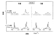
図3は、4H-SiC単結晶基板に波長244nm(SiC単結晶基板への侵入長はおよそ200nm)のレーザー光を照射して得られたラマン散乱光スペクトルである。ラマン振動数を波数表記すると、4H-SiCの結晶構造に固有の波数に対応したラマン線が得られている。
各固有波数で検出されたラマン線の強度は、(000-1)面から得られるラマン線の方が(0001)面から得られるラマン線と比較して強い。
このことから、(0001)面および(000-1)面を有するが裏表のどちらがいずれの面であるかが不明なSiC単結晶基板に対して、固有波数でのラマン強度を測定することでSiC単結晶基板の裏表のいずれが(0001)面であり他方が(000-1)面であることを判定できる。
FIG. 3 is a Raman scattered light spectrum obtained by irradiating a 4H-SiC single crystal substrate with laser light having a wavelength of 244 nm (the penetration length into the SiC single crystal substrate is approximately 200 nm). When the Raman frequency is expressed as a wave number, a Raman line corresponding to the wave number unique to the crystal structure of 4H-SiC is obtained.
The intensity of the Raman line detected at each natural wave number is stronger in the Raman line obtained from the (000-1) plane than in the Raman line obtained from the (0001) plane.
From this, SiC intensity is measured by measuring the Raman intensity at the natural wave number of a SiC single crystal substrate with (0001) plane and (000-1) plane, but which side is unclear. It can be determined that either the front or back of the single crystal substrate is the (0001) plane and the other is the (000-1) plane.
また、図3において200cm-1付近の折り返しモード域に存在するダブレットは、(0001)面から得られるラマン散乱光スペクトルでは低波数側の強度が高波数側と比較して大きく、(000-1)面から得られるラマン散乱光スペクトルでは高波数側の強度が低波数側と比較して大きい。
このことから、(0001)面または(000-1)面を有してはいるが、どちからが不明なSiC単結晶基板に対して、折り返しモード域に存在するダブレットの強度比を測定することで、該SiC単結晶基板の表面が(0001)面か(000-1)面のどちらかを判定できる。
Further, in FIG. 3, the doublet existing in the folding mode region near 200 cm −1 has a higher intensity on the low wave number side than the high wave number side in the Raman scattered light spectrum obtained from the (0001) plane, and is (000-1 ) In the Raman scattered light spectrum obtained from the surface, the intensity on the high wave number side is larger than that on the low wave number side.
From this, measure the strength ratio of doublets existing in the folding mode region for SiC single crystal substrates that have (0001) or (000-1) planes but are unknown. Thus, it can be determined whether the surface of the SiC single crystal substrate is the (0001) plane or the (000-1) plane.
図4は、4H-SiC、6H-SiCおよび15R-SiC単結晶基板に対して波長244nmのレーザー光を照射して得られたラマン散乱光スペクトルのうち、各ポリタイプに固有の折り返しモード域でのダブレットを示している。
4H-SiCにおいては、上記で記したように200 cm-1付近のダブレットは、(0001)面から得られるラマン線の場合は低波数側のラマン線強度の方が高波数側のラマン線強度と比較して大きく、(000-1)面から得られるラマン線の場合は高波数側のラマン線強度が低波数側のラマン線強度と比較して大きい。
Figure 4 shows the folding mode region unique to each polytype in the Raman scattered light spectrum obtained by irradiating 4H-SiC, 6H-SiC and 15R-SiC single crystal substrates with laser light having a wavelength of 244 nm. Shows a doublet.
In 4H-SiC, as described above, in the doublet near 200 cm -1 , in the case of the Raman line obtained from the (0001) plane, the Raman line intensity on the low wave number side is higher than the Raman line intensity on the high wave number side. In the case of a Raman line obtained from the (000-1) plane, the Raman line intensity on the high wave number side is larger than the Raman line intensity on the low wave number side.
6H-SiCにおいては、500 cm-1付近の折り返しモード域のダブレットでは、(高波数側から得られるラマン線強度/低波数側から得られるラマン線強度)の比は(0001)面から得られるラマン線の方が(000-1)面から得られるラマン線と比較して小さい。 In 6H-SiC, the ratio of (Raman line intensity obtained from the high wave number side / Raman line intensity obtained from the low wave number side) ratio is obtained from the (0001) plane in the doublet in the folded mode region near 500 cm -1. The Raman line is smaller than the Raman line obtained from the (000-1) plane.
15R-SiCの場合は、570 cm-1付近の折り返しモード域のダブレットでは、(0001)面から得られるラマン線の場合は低波数側のラマン線強度の方が高波数側のラマン線強度と比較して小さく、(000-1)面から得られるラマン線の場合は高波数側のラマン線強度が低波数側のラマン線強度と比較して小さい。
また、850 cm-1付近の折り返しモード域のダブレットでは、(高波数側から得られるラマン線強度/低波数側から得られるラマン線強度)の比は(0001)面から得られるラマン線の方が(000-1)面から得られるラマン線と比較して大きい。さらに930 cm-1付近の折り返しモード域のダブレットでは、(0001)面から得られるラマン線の場合は高波数側のラマン線強度の方が低波数側のラマン線強度と比較して小さく、(000-1)面から得られるラマン線の場合は低波数側のラマン線強度が高波数側のラマン線強度と比較して小さい。
In the case of 15R-SiC, in the doublet in the folded mode region near 570 cm -1 , the Raman line intensity on the low wave number side is higher than the Raman line intensity on the high wave number side in the case of the Raman line obtained from the (0001) plane. In the case of a Raman line obtained from the (000-1) plane, the Raman line intensity on the high wave number side is smaller than the Raman line intensity on the low wave number side.
In the doublet in the folded mode region near 850 cm -1, the ratio of (Raman line intensity obtained from the high wave number side / Raman line intensity obtained from the low wave number side) is the ratio of the Raman line obtained from the (0001) plane. Is larger than the Raman line obtained from the (000-1) plane. Furthermore, in the doublet in the folded mode region near 930 cm −1, the Raman line intensity on the high wave number side is smaller than the Raman line intensity on the low wave number side in the case of the Raman line obtained from the (0001) plane, In the case of the Raman line obtained from the (000-1) plane, the Raman line intensity on the low wave number side is smaller than the Raman line intensity on the high wave number side.
図5には、15R-SiC単結晶基板に波長488(SiC単結晶基板への侵入長は1μm以上)および244nmのレーザー光を照射して得られたラマン散乱光スペクトルのうち、15R-SiC単結晶構造に固有の折り返しモード域でのダブレットを示している。
波長244nmおよび266nm(SiC単結晶基板への侵入長はおよそ400nm)のレーザー光を用いた場合には、上述の折り返しモード域におけるダブレットの強度比が(0001)面および(000-1)面で異なって検出されている。
Fig. 5 shows the 15R-SiC single crystal out of the Raman scattered light spectrum obtained by irradiating a 15R-SiC single crystal substrate with a laser beam of wavelength 488 (penetration length of 1 μm or more into the SiC single crystal substrate) and 244 nm. A doublet in the folding mode region inherent to the crystal structure is shown.
When using laser beams with wavelengths of 244 nm and 266 nm (the penetration length into the SiC single crystal substrate is approximately 400 nm), the intensity ratio of the doublet in the above folding mode region is (0001) plane and (000-1) plane Detected differently.
しかしながら波長が325nmより長い(SiC単結晶基板への侵入長が1μm以上)レーザー光を用いた場合には、折り返しモード域におけるダブレットの強度比は、(0001)面および(000-1)面で差異を認めにくい。
これは、SiC単結晶基板に対して波長が325nmを超えるレーザー光は侵入長が深く、バルクフォノンモードを主として検出するためである。したがって、より短波長である244nmおよび266nmのレーザー光を使用することで侵入長を浅くし、表面モードを主として検出するのが良い。
このように300nmより短い波長のレーザー光を励起光として用いて折り返しモード域における複数のラマン線の強度比を計測することで、SiC単結晶の面極性判定をできる。
However, when using a laser beam with a wavelength longer than 325 nm (penetration length of 1 μm or more into the SiC single crystal substrate), the intensity ratio of the doublet in the folded mode region is (0001) plane and (000-1) plane. Difficult to recognize differences.
This is because laser light having a wavelength of more than 325 nm with respect to the SiC single crystal substrate has a deep penetration depth and mainly detects the bulk phonon mode. Therefore, it is preferable to detect the surface mode mainly by using a shorter wavelength of 244 nm and 266 nm laser light to reduce the penetration depth.
Thus, the plane polarity of the SiC single crystal can be determined by measuring the intensity ratio of a plurality of Raman lines in the folding mode region using laser light having a wavelength shorter than 300 nm as excitation light.
上記においては、主としてSiC単結晶の、極性半導体の面極性の判定について説明してきたが、SiC単結晶以外の、極性半導体の面極性の判定にも適用することができる。例えば、InN,GaN、AlN(III-V族)、ZnS(II-VI族)などである。
特に、InN,GaN、AlN(III-V族)、ZnS(II-VI族)など原子量の異なる2原子からなる化合物半導体では、最表面原子層が軽い原子か重い原子かによって振動振幅が大きく異なるため、ラマン散乱光の強度は面極性により異なる。
また、これらの化合物半導体が長周期構造を有する極性化合物半導体である場合には、折り返しモード域のダブレットが存在し、それらの強度比は面極性により異なる。そのため、本発明により、面極性を非破壊非接触にて判定することが可能である。
In the above description, the determination of the plane polarity of the polar semiconductor mainly of the SiC single crystal has been described, but the present invention can also be applied to the determination of the plane polarity of polar semiconductors other than the SiC single crystal. For example, InN, GaN, AlN (III-V group), ZnS (II-VI group) and the like.
In particular, in compound semiconductors consisting of two atoms with different atomic weights such as InN, GaN, AlN (III-V group), ZnS (II-VI group), the vibration amplitude varies greatly depending on whether the outermost atomic layer is a light atom or a heavy atom. Therefore, the intensity of Raman scattered light varies depending on the surface polarity.
In addition, when these compound semiconductors are polar compound semiconductors having a long-period structure, there are doublet in the folded mode region, and the intensity ratio thereof varies depending on the plane polarity. Therefore, according to the present invention, the surface polarity can be determined in a non-destructive and non-contact manner.
この場合、励起光の侵入長は該単結晶基板の吸収係数により決定されるため、該単結晶基板の吸収係数を考慮して波長を決定する必要がある。
その際、バルク結晶内フォノンモードと比較して表面振動モードを主として検出するためには短波長の励起光を用いることが望ましい。すなわち、そのために励起光として該単結晶基板の吸収係数の逆数が400nm以下となる波長を励起光として用いることが、より望ましいことが分る。
In this case, since the penetration length of the excitation light is determined by the absorption coefficient of the single crystal substrate, it is necessary to determine the wavelength in consideration of the absorption coefficient of the single crystal substrate.
At that time, in order to mainly detect the surface vibration mode as compared with the phonon mode in the bulk crystal, it is desirable to use excitation light having a short wavelength. That is, it is more desirable to use as the excitation light a wavelength at which the reciprocal of the absorption coefficient of the single crystal substrate is 400 nm or less.
本発明は、極性半導体に励起光を照射して得られるラマン散乱光スペクトルを測定することにより、面極性の判定を行い、非破壊かつ非接触で面極性の判定を可能し、また高空間分解能での判定が可能になり、さらに測定部位を該単結晶基板面上で移動させることにより、容易に単結晶基板全体の面極性分布を測定することが可能であり、短時間で面極性の判定ができるという著しい効果があるので、極性半導体の面極性判定方法に極めて有用である。 The present invention makes it possible to determine the surface polarity by measuring the Raman scattered light spectrum obtained by irradiating the polar semiconductor with excitation light, and to determine the surface polarity in a non-destructive and non-contact manner. In addition, it is possible to easily measure the surface polarity distribution of the entire single crystal substrate by moving the measurement site on the surface of the single crystal substrate. Therefore, the present invention is extremely useful for a method for determining the surface polarity of a polar semiconductor.
Claims (4)
Priority Applications (1)
| Application Number | Priority Date | Filing Date | Title |
|---|---|---|---|
| JP2005260379A JP4635158B2 (en) | 2005-09-08 | 2005-09-08 | Method for determining surface polarity of polar semiconductors |
Applications Claiming Priority (1)
| Application Number | Priority Date | Filing Date | Title |
|---|---|---|---|
| JP2005260379A JP4635158B2 (en) | 2005-09-08 | 2005-09-08 | Method for determining surface polarity of polar semiconductors |
Publications (2)
| Publication Number | Publication Date |
|---|---|
| JP2007071747A JP2007071747A (en) | 2007-03-22 |
| JP4635158B2 true JP4635158B2 (en) | 2011-02-16 |
Family
ID=37933304
Family Applications (1)
| Application Number | Title | Priority Date | Filing Date |
|---|---|---|---|
| JP2005260379A Expired - Fee Related JP4635158B2 (en) | 2005-09-08 | 2005-09-08 | Method for determining surface polarity of polar semiconductors |
Country Status (1)
| Country | Link |
|---|---|
| JP (1) | JP4635158B2 (en) |
Families Citing this family (1)
| Publication number | Priority date | Publication date | Assignee | Title |
|---|---|---|---|---|
| CN106546415A (en) * | 2016-11-09 | 2017-03-29 | 石长海 | A kind of quartz wafer(Block)The instrument of non-contact detection positive-negative polarity |
Family Cites Families (2)
| Publication number | Priority date | Publication date | Assignee | Title |
|---|---|---|---|---|
| JP3658832B2 (en) * | 1996-02-13 | 2005-06-08 | 株式会社デンソー | Silicon carbide single crystal manufacturing apparatus and silicon carbide single crystal manufacturing method |
| JP4157326B2 (en) * | 2002-05-27 | 2008-10-01 | 新日本製鐵株式会社 | 4H type silicon carbide single crystal ingot and wafer |
-
2005
- 2005-09-08 JP JP2005260379A patent/JP4635158B2/en not_active Expired - Fee Related
Also Published As
| Publication number | Publication date |
|---|---|
| JP2007071747A (en) | 2007-03-22 |
Similar Documents
| Publication | Publication Date | Title |
|---|---|---|
| JP6197722B2 (en) | Method for evaluating in-plane distribution of dislocations in SiC plate | |
| JP5000424B2 (en) | Defect detection method for silicon carbide single crystal wafer and method for manufacturing silicon carbide semiconductor element | |
| US10048142B2 (en) | Evaluation method for bulk silicon carbide single crystals and reference silicon carbide single crystal used in said method | |
| Momeni Pakdehi et al. | Silicon Carbide Stacking‐Order‐Induced Doping Variation in Epitaxial Graphene | |
| CN111048431B (en) | Evaluation method of SiC substrate and manufacturing method of SiC epitaxial wafer | |
| JP6986944B2 (en) | Evaluation method and manufacturing method of SiC epitaxial wafer | |
| García Núñez et al. | Surface optical phonons in GaAs nanowires grown by Ga-assisted chemical beam epitaxy | |
| Tuominen et al. | Crystalline imperfections in 4H SiC grown with a seeded Lely method | |
| JP2014002104A (en) | METHOD FOR EVALUATING SiC SINGLE CRYSTAL SUBSTRATE AND SiC EPITAXIAL WAFER, METHOD FOR MANUFACTURING SiC SINGLE CRYSTAL AND SiC EPITAXIAL WAFER, AND SiC SINGLE CRYSTAL | |
| Wang et al. | 2D XANES-XEOL mapping: observation of enhanced band gap emission from ZnO nanowire arrays | |
| Kondo et al. | Development of RAF quality 150mm 4H-SiC wafer | |
| KR102567624B1 (en) | Silicon carbide crystal defect location analysis method using non-destructive analysis method and analysis device and computer program including the same | |
| Seredin et al. | S2-semipolar GaN grown by HVPE on a non-polar m-plane sapphire: Features of growth and structural, morphological, and optical properties | |
| JP4635158B2 (en) | Method for determining surface polarity of polar semiconductors | |
| Talwar et al. | Spectroscopic phonon and extended x-ray absorption fine structure measurements on 3C-SiC/Si (001) epifilms | |
| Feenstra et al. | Porous silicon carbide and gallium nitride: epitaxy, catalysis, and biotechnology applications | |
| Rakhlin et al. | Allotropic Ga 2 Se 3/GaSe nanostructures grown by van der Waals epitaxy: narrow exciton lines and single-photon emission | |
| Warrier et al. | Determination of thermal and electronic carrier transport properties of SnS thinfilms using photothermal beam deflection technique | |
| Filintoglou et al. | Size control of GaN nanocrystals formed by ion implantation in thermally grown silicon dioxide | |
| Wei et al. | Growth oscillation of MoSe2 monolayers observed by differential reflectance spectroscopy | |
| JP2011149698A (en) | Window member for terahertz waveband, sample container, detection and generation device, substrate material, and method for calculating and evaluating transmission characteristics of single crystal silicon carbide | |
| Sahu et al. | Ultraviolet photoluminescence from stressed silicon nanoclusters | |
| Wang et al. | Quantitative comparison between dislocation densities in offcut 4H-SiC wafers measured using synchrotron x-ray topography and molten KOH etching | |
| Kundu et al. | Boron doped SiC thin film on Silicon synthesized from polycarbosilane: a new lead free material for applications in piezosensors | |
| JP2020063186A (en) | SiC epitaxial wafer |
Legal Events
| Date | Code | Title | Description |
|---|---|---|---|
| A621 | Written request for application examination |
Free format text: JAPANESE INTERMEDIATE CODE: A621 Effective date: 20080305 |
|
| A977 | Report on retrieval |
Free format text: JAPANESE INTERMEDIATE CODE: A971007 Effective date: 20100402 |
|
| A131 | Notification of reasons for refusal |
Free format text: JAPANESE INTERMEDIATE CODE: A131 Effective date: 20100727 |
|
| A521 | Request for written amendment filed |
Free format text: JAPANESE INTERMEDIATE CODE: A523 Effective date: 20100917 |
|
| RD02 | Notification of acceptance of power of attorney |
Free format text: JAPANESE INTERMEDIATE CODE: A7422 Effective date: 20100917 |
|
| TRDD | Decision of grant or rejection written | ||
| A01 | Written decision to grant a patent or to grant a registration (utility model) |
Free format text: JAPANESE INTERMEDIATE CODE: A01 Effective date: 20101019 |
|
| A01 | Written decision to grant a patent or to grant a registration (utility model) |
Free format text: JAPANESE INTERMEDIATE CODE: A01 |
|
| A61 | First payment of annual fees (during grant procedure) |
Free format text: JAPANESE INTERMEDIATE CODE: A61 Effective date: 20101022 |
|
| FPAY | Renewal fee payment (event date is renewal date of database) |
Free format text: PAYMENT UNTIL: 20131203 Year of fee payment: 3 |
|
| R150 | Certificate of patent or registration of utility model |
Free format text: JAPANESE INTERMEDIATE CODE: R150 |
|
| FPAY | Renewal fee payment (event date is renewal date of database) |
Free format text: PAYMENT UNTIL: 20131203 Year of fee payment: 3 |
|
| R250 | Receipt of annual fees |
Free format text: JAPANESE INTERMEDIATE CODE: R250 |
|
| S533 | Written request for registration of change of name |
Free format text: JAPANESE INTERMEDIATE CODE: R313533 |
|
| R350 | Written notification of registration of transfer |
Free format text: JAPANESE INTERMEDIATE CODE: R350 |
|
| R250 | Receipt of annual fees |
Free format text: JAPANESE INTERMEDIATE CODE: R250 |
|
| LAPS | Cancellation because of no payment of annual fees |