JP4629938B2 - EMI reduction by switching frequency dithering - Google Patents
EMI reduction by switching frequency dithering Download PDFInfo
- Publication number
- JP4629938B2 JP4629938B2 JP2001524278A JP2001524278A JP4629938B2 JP 4629938 B2 JP4629938 B2 JP 4629938B2 JP 2001524278 A JP2001524278 A JP 2001524278A JP 2001524278 A JP2001524278 A JP 2001524278A JP 4629938 B2 JP4629938 B2 JP 4629938B2
- Authority
- JP
- Japan
- Prior art keywords
- frequency
- switching
- switching frequency
- register
- selecting
- Prior art date
- Legal status (The legal status is an assumption and is not a legal conclusion. Google has not performed a legal analysis and makes no representation as to the accuracy of the status listed.)
- Expired - Fee Related
Links
Images


Classifications
-
- H—ELECTRICITY
- H02—GENERATION; CONVERSION OR DISTRIBUTION OF ELECTRIC POWER
- H02M—APPARATUS FOR CONVERSION BETWEEN AC AND AC, BETWEEN AC AND DC, OR BETWEEN DC AND DC, AND FOR USE WITH MAINS OR SIMILAR POWER SUPPLY SYSTEMS; CONVERSION OF DC OR AC INPUT POWER INTO SURGE OUTPUT POWER; CONTROL OR REGULATION THEREOF
- H02M1/00—Details of apparatus for conversion
- H02M1/44—Circuits or arrangements for compensating for electromagnetic interference in converters or inverters
-
- H—ELECTRICITY
- H02—GENERATION; CONVERSION OR DISTRIBUTION OF ELECTRIC POWER
- H02M—APPARATUS FOR CONVERSION BETWEEN AC AND AC, BETWEEN AC AND DC, OR BETWEEN DC AND DC, AND FOR USE WITH MAINS OR SIMILAR POWER SUPPLY SYSTEMS; CONVERSION OF DC OR AC INPUT POWER INTO SURGE OUTPUT POWER; CONTROL OR REGULATION THEREOF
- H02M1/00—Details of apparatus for conversion
- H02M1/12—Arrangements for reducing harmonics from ac input or output
-
- H—ELECTRICITY
- H04—ELECTRIC COMMUNICATION TECHNIQUE
- H04B—TRANSMISSION
- H04B15/00—Suppression or limitation of noise or interference
- H04B15/02—Reducing interference from electric apparatus by means located at or near the interfering apparatus
- H04B15/04—Reducing interference from electric apparatus by means located at or near the interfering apparatus the interference being caused by substantially sinusoidal oscillations, e.g. in a receiver or in a tape-recorder
-
- H—ELECTRICITY
- H04—ELECTRIC COMMUNICATION TECHNIQUE
- H04B—TRANSMISSION
- H04B2215/00—Reducing interference at the transmission system level
- H04B2215/064—Reduction of clock or synthesizer reference frequency harmonics
- H04B2215/067—Reduction of clock or synthesizer reference frequency harmonics by modulation dispersion
Description
【0001】
【従来技術】
全ての商業的電気システムは、特定の電磁干渉(EMI)制約を満たさねばならない。EMI解決策には大抵の場合かなり費用がかかる。システムの中には、費用全体の30%が大型フィルタやシールディングなどのEMI/EMC(互換性)関連であるというものもある。電動パワーステアリング(EPS)システムでは、RFノイズに大きく寄与しているのは、電流制御に使用されるパルス幅変調(PWM)作用である。PWMは、狭帯域ノイズをPWMスイッチング周波数の整数高調波毎にスパイクという形で発生させる。上記の高調波はラジオの出力に明確な信号音として現れることから、車両のラジオは狭帯域ノイズによって相当な被害を被ることになる。この発明は狭帯域ノイズを広帯域ノイズに変換し、PWMのスイッチング周波数を狭い範囲内で変化させることによりそのピーク振幅を小さくする。
【0002】
PWM高周波スパイクは、
【0003】
【数1】
![]()
により与えられる振幅を有し、ここにAはパルスの振幅、tはPWM「オン」タイム、TsはPWMスイッチング期間、fnは1/Ts、即ちスイッチング周波数fs、の整数倍数である。スペクトルは、fnだけ間隔の空いた一連のスパイクであり、図1に見られるように正弦波形状の包絡線のモジュラスにより限度を画定されている。
【0005】
【課題を解決するための手段】
パルス変調制御型の自動車モーターにより発生するする電磁干渉の帯域幅を制御する方法を開示する。本方法は、少なくとも1つのレジスタを含んでいる制御装置であって、その動作パラメータに基づいてモーターを制御するためにモーターと信号通信する制御装置を提供する工程と、第1のクロック周波数を選択する工程と、第1のスイッチング周波数を選択する工程と、少なくとも1つのレジスタを初期化し、それにより、定められた少なくとも1つの数を設定する工程と、第1のホッピング期間を選択する工程と、少なくとも1つのレジスタの定められた少なくとも1つの数、第1のクロック周波数、及び第1のホッピング周波数に基づいて、パルス変調のスイッチング周波数をランダムに変調する工程と、を備えている。
【0006】
【発明の実施の形態】
PWM周波数「ディザリング」のコンセプトは、特定のPWMスイッチング周波数fsを、別のスイッチング周波数fsに変更する前の設定数分のPWMスイッチング期間Tsの間だけ使用し、この「ホップ」を周期的に行うことを包含している。使用される各スイッチング周波数fsは、固有の高調波成分の分だけ寄与するが、絶えず使用されるわけではないので、等価振幅はずっと低くなる。最終的には、ピーク振幅がより低い連続するスペクトルという結果になる。
【0007】
ディザリング処理はシステム全体の費用を低減する。ディザリングは、追加的な構成要素を何ら必要とするわけではなく、ソフトウェアにより実現される。より大きなRFノイズの振幅を許容しながら、同時に放出のピークレベルを低下させるので、フィルタリング及びシールディングに要する費用を低減させることができる。
【0008】
PWM周波数ディザリングには多くのパラメータが関係するが、それらには、スイッチング周波数範囲、使用されるスイッチング周波数の数、ホッピング周波数、及び周波数選択のやり方などが挙げられる。理想的なケースとしては、利用できるスイッチング周波数が無限(連続分布)にあり、その間で非常に素早く変更し、その中からランダムに選択できる場合が考えられる。この場合、RFノイズは、振幅が狭帯域のピークの場合よりも低い、純粋な広帯域になる。
【0009】
都合の悪いことに、理想的な状態は実現不可能なので、システム要求と広帯域の理想との間に妥協を図らねばならない。EPSシステムは、現実的にはランダム選択をすることは不可能であり、ある一定数の個別のスイッチング周波数でしか作動できない。スイッチング周波数を非常に迅速に変えれば、スループット及び安定性の問題が発生することになる。ある範囲内で擬似ランダム数の表を生成すれば、シーケンスがサブ変調を発生させるほどには速く反復できないことを保証することにより、スイッチング周波数のランダム選択を模することができる。
【0010】
シミュレーション及び理論的な計算を使って結果を予想した。しかしながら、信頼できる結果はラジオの音声出力である。連結媒体とラジオ挙動の正確なモデルを導き出すことはできるが、人間の耳の主観的な特性はモデル化が容易ではない。従って、何れの周波数ディザリングフォーマットでも実際のメリットは最終的な産物、即ちそれがどのように聞こえるかということである。以下の結果が得られた。即ち、
1)ホッピング周波数fhは最も重要な因子である。ノイズの「サウンド」はこのホッピング周波数に大きく左右される。相当にホワイトなサウンドノイズが500μs未満のホッピング期間で実現された。
2)わずか2通りのスイッチング周波数を使って、ラジオの出力の信号音を排除することができる(その間のΔfについては#3を参照)。
3)選択対象となる周波数の範囲は、ラジオのIF帯域幅、ラジオのRF周波数範囲、及び凡そのPWM基本特性により決まる。スイッチング範囲は、ラジオのRF入力に対応する高調波数を掛けると、それがIF帯域幅を上回るように、十分に大きくなければならない。例えば、PWMが20kHz付近でIF帯域幅が9kHzでRFが150kHzの場合(ヨーロッパのLWの場合)には、使用されるスイッチング周波数の範囲は9kHz×20kHz/150kHz=1.2kHzよりも大きくなければならない。これは使用できる最小値であり、最大値はシステムの安定性によって異なる。
4)使用される個々のスイッチング周波数の数が増加すれば結果は向上するが、個数が非常に多い場合には益が薄れる。
【0011】
図3は固定周波数PWMにより発生した信号音を示し、図4は、擬似ランダム的に250μs毎に選択された、16のスイッチング周波数fsからのボリュームが低減された「ホワイトノイズ」を示している。ディザリング処理はシステム全体の費用を低減する。ティザリングは、追加的な構成要素を何ら必要とするわけではなく、ソフトウェアにより実現される。より大きなRFノイズの振幅を許容しながら、同時に放出のピークレベルを低下させるので、フィルタリング及びシールディングに要する費用を低減させることができる。
【0012】
固定周波数(標準)PWMでは、数式1及び図1に示すように、スイッチング周波数の整数倍数毎に高調波が発生する。ラジオ受信機及び他の電子機器は、特定の周波数に集束されるこの狭帯域ノイズに敏感である。AMラジオ局が純音を流した場合、その結果として現れるスペクトルを図5に示す。ラジオのIF帯域幅は中心が搬送波周波数fcにあり、より小さなスパイク(側波帯)は両方とも9kHz帯域幅内に納まるので、ラジオは1kHz信号音をデコードする。パルス幅変調から放射された高調波がラジオ局の周波数に近いときには、ラジオはそれを全く同じ様式の可聴信号音として復調する。
【0013】
スイッチング周波数ディザリングは、パルス幅変調(PWM)の代わりの方法である。その目的は、放射されたRFエネルギーをより大きな周波数範囲(広帯域)に広げ、その結果としてのEMIをホワイトノイズと同じようにすることである。ラジオ受信機は、ノイズ帯域幅がIF帯域幅よりもずっと大きいので、このタイプのEMIに対してはそれほど敏感ではない。PWMに関しては、スイッチング期間Tsには「オン」タイムと「オフ」タイムが含まれる。これら2つのタイムの合計がスイッチング期間Tsとなる。電流は、オンタイムとオフタイムの比、即ちデューティレシオDを変化させることにより制御される。従って、
【0014】
【数2】

標準的なPWM実施例では、スイッチング期間Tsは一定で、デューティレシオDのみが変化する。スイッチング周波数ディザリングは、Tsを変更する処理である。これは、電流の制御スキームとは独立して行われる。例えば、一定電流はDを変化させずにTsを変化させることを意味し、オンタイムとオフタイムが同時に変更されることになる。
【0016】
ディザリング実施に関係するパラメータには以下のものが含まれる。
【0017】
【表1】
スイッチング周波数ディザリングの理想的な実施には、大きく連続した分布からランダムに選定されたスイッチング周波数fs、その中でのできる限り速いホッピング、が関わることになる。合成されたスペクトルは、ピークレベルが狭帯域のピークレベルよりも低い純帯域幅となる。
【0019】
ホッピング周波数fhはできる限り高いほうがよい。唯一限定を課せられる因子はスイッチング周波数fsである。最も高速で実施できるのは、別のスイッチング周波数に「ホップ」する前に、1つのスイッチング期間Tsでは1つのスイッチング周波数fsしか使用しない場合である。このホッピング周波数fhを正確に知るためには、スイッチング周波数fsをホッピング周波数fhの整数倍数として特定的に選定しなければならない。EPSには、音声及び熱的な問題により18kHz<fs<30kHzという拘束条件が課せられるので、高いホッピング周波数では使用できるスイッチング周波数の数が限られる。フレキシブルなホッピング周波数を使用すればこの問題は解決される。新しいスイッチング周波数fsへのホップは、スイッチング期間Tsの終了時しか起こりえないので、新たなスイッチング周波数fsはここで開始される。一例として、ホッピング期間(Th=1/fh)は500μsであると仮定すると、fs1=19.5kHzでfs2=21kHzとなる。19.5kHzは9期間続き合計で462μsとなる。第10期間の間に500μsマークに達し、合計513μsでこの期間は終了する。次にパルス幅変調は524μs(11期間)に対し21kHzで起きる。ホッピング周波数は約2kHz変化することに留意されたい。これとは別に、このフレキシブルなホッピング周波数は、システムの構成要素の可聴信号音の変調処理を省く手助けもする。
【0020】
スイッチング周波数が継続的に分布(N=∞)しているのが理想的である。ある電動パワーステアリングシステム(EPS)では、周波数は数式2を満たすことができ、ここにfsがスイッチング周波数でnが整数である。
【0021】
【数3】
18kHz未満は禁制音声範囲であり、25kHzより上は熱性能上不利である。これは、32の可能性のあるスイッチンング周波数があるが、約10から20に絞りこめば、合計周波数範囲を制限することによりシステムの安定性が改善できるということを示唆している。
【0023】
放射の対象となっている最も低い周波数帯域によって、必要とされるスイッチング周波数fsの範囲が決まる。広帯域という用語は、RFスペクトルが連続し且つギャップが無い状態のことを指す。これを実現するには、PWM基本周波数のn番目の高調波が、対象となる周波数帯の(n+1)番目の高調波と重なっていなければならない。スペクトルは、上の数式の周波数fintより上では相当平坦な広帯域である。例えば、最小スイッチング周波数は18kHzで最大スイッチング周波数が21kHzであれば、スペクトルは約126kHzより上で平ら(ギャップがない)となる。従って、
【0024】
【数4】
![]()
である。
ディザリング処理の最後のパラメータは、スイッチング周波数が使用される順序である。理想的には、この選択はランダム式であろうが、EPS制御装置ではこれを実現できない。幸運にも、擬似ランダム選択がこれに適する。所与の順序でスイッチング周波数内をステッピングすると、一連の長さが十分でない場合には音声範囲にサブ変調が生じる。あるパターンは、反復前に(fh<2000hz)少なくとも0.5msを要する。この理由により、ルックアップ表又は擬似ランダム生成が適切であるといえる。
【0026】
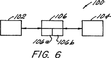
図6では、パルス幅変調周波数ディザリングを行うためのシステム100の関連部分は、EPS制御装置102とEPSモーター104である。制御装置102の内部には、モーター104への電流を切り替えるために使用されるパワーMOSFET(例示的に図12の500に図示)がある。ブラシレスモーター駆動(BMD)集積回路(IC)106は、電圧モードリセット方式又は電流モードリセット方式の何れかでこれらスイッチを制御する。BMDIC106の中には2つのレジスタ106a、106bがある。第1のレジスタ106aは、デューティレシオDを設定するためのもので、第2のレジスタ106bは、スイッチング期間Ts用である。これらのレジスタ106a、106bは、それぞれ数N1、N2を保有しており、ICは、2.097MHzクロックでこの数まで「カウント」せねばならない。スイッチング期間Tsの開始時には、適切なMOSFET500が、モーター104の位置及び所望の回転方向に基づいて起動される。デューティレシオレジスタ106b内の値により規定された時間量Δt1=N1/fclkが経過した後、これらのMOSFET500は作動停止される。クロックは、スイッチング期間レジスタ106aにより規定された時間量Δt2=N2/fclkが満了するまで走り続ける。この時点で、スイッチング期間Tsはリセットされ、MOSFET500は再度起動される。これら2つのレジスタ106a、106bを比例的に変更することにより、スイッチング周波数fsは、モーター104への電流レベルを変えることなく、変更できる。
【0027】
しかしながら、デューティレシオレジスタ106bが、MOSFET500をオフにするよう常にトリガするわけではない。時には、モーター104への電流レベルがリセットをトリガする。このモードでは、スイッチング周波数fsの変更を行うと、平均(DC)電流レベルに小さな変化が生じる。これらの変化は、音声変調を引き起こし、それがモーター104から聞こえることになる。制御装置102が数個のスイッチング周波数fsの間だけで変化するのであれば、ホッピング周波数fhの2分の1の信号音がモーター104で聞こえることになる。数個のスイッチング周波数を使用し、その擬似ランダム選択を行うことにより、モーター104からのノイズは幾分ホワイトノイズ的になり、不快感がかなり緩和される。
【0028】
制御装置102のマイクロプロセッサは、バス102aに沿ってBMDIC106と周期的に逐次通信を行う。新しいスイッチング周波数コマンドが、ホッピング期間Th、例えば500μsの終わりにBMDIC106に送られ、こうしてスイッチング周波数106aを更新する。必要であれば、デューティレシオレジスタ106bも更新される。次のスイッチング期間Tsは、新しいスイッチング周波数fsとなる。
【0029】
2つの周波数ディザリング方法が提供されている。両方共に、同じスイッチング周波数fsを使い、それらの間で同じホッピング周波数fhでスイッチする。両方法の違いは、それぞれがシステムメモリとスループットに課す要求である。第1のディザリング方法では、メモリは、BMDIC106内へ順次ロードされるスイッチング周波数のリストを保有する。リスト中の各値は、幾つかの可能性の中からランダムに選定されたものである。作成された後、リストはソフトウェアの一部として永久的に保存される。第2のディザリング方法では、シフトレジスタ200が、モジュロ2合算関数202と組み合わせられて、図7に示すような線形のフィードバックレジスタを形成する。レジスタビットの内の4つは、XOR処理され8ビットレジスタへの入力を形成し、255記号長の擬似ランダムシーケンスを作り出す。シフトレジスタ200の中身のうち半分は、図8の表に示すように、16個の可能なスイッチング周波数fsと1対1の関係に4ビット出力204を形成する。16個のスイッチング周波数レジスタコマンドは、ソフトウェアの一部である。図8では、左から4列が、シフトレジスタ200からの4ビット出力を表している。表の「HEX」と標示された行は、スイッチング周波数レジスタ106aに供給されるスイッチング周波数の16進値を示している。表の「DEC」と標示された列は、先に述べた16進値の10進法表現を示している。表の「カウンタサイクル」と標示された列は、16進値の最後の2桁の10進法表現を示している。fsと標示された列は、
2.0970÷カウンタサイクル=fs Mhz (4)
となるようなスイッチング周波数を表している。
【0030】
本発明の方法の一般化されたフロー線図300を図9に示す。ボックス302で、第1のレジスタ106aが規定数の有限セットから第1の規定数N1に初期化され、第2のレジスタ106bは規定数の有限セットから第2の規定数N2に初期化される。ブロック304で、第1のクロック周波数fclkが選択され、第1のホッピング期間Thが選択され、第1のスイッチング周波数fslがスイッチング周波数の有限セットから選択される。ブロック306では、規定された第1及び第2の数N1とN2、第1のクロック周波数fclk、第1のスイッチング周波数fs1、及び第1のホッピング期間Thに基づいて、モーター104がパルス幅変調により第1のスイッチング周波数fs1で制御される。ブロック308では、まだホッピング期間Thが経過していなければ、モーター104は、パルス幅変調により第1のスイッチング周波数fs1で引き続き制御される。既にThが経過していればブロック308aで、既にスイッチング期間Tsが経過していればブロック310で、第1及び第2のレジスタ106a、106bは、マイクロプロセッサ102からのコマンドに応えて少なくとも擬似ランダム的に第3の規定数N3及び第4の規定数N4に再度初期化され、これにより、少なくとも擬似ランダム的に第1スイッチング周波数fs1が第2のスイッチング周波数fs2に変更され、従って、モーター104がパルス幅変調により第2のスイッチング周波数fs2で制御されることになる。ブロック308bでは、スイッチング期間Tsの経過を待って、第1及び第2のレジスタ106a、106bが再度初期化される。新しいスイッチング周波数fs2でのモーター104のパルス幅変調制御は、ホッピング期間Thとスイッチング期間Tsが再度経過するまで継続され、マイクロプロセッサからコマンドがあれば、第3の規定数N3と第4の規定数N4は、これにより少なくとも擬似ランダム的にN5及びN6に変更され、その結果、少なくとも擬似ランダム的に第2のスイッチング周波数fs2は第3のスイッチング周波数fs3に変更され、従って、モーター104はパルス幅変調により第3のスイッチング周波数fs3で制御されることになる。先に述べた連続擬似ランダムスイッチング周波数fsiでのモーター104のパルス幅変調は、第1及び第2レジスタ106a、106bがホッピング期間Thの終わりに規定数Niで再度初期化されるサイクル様式で継続される。
【0031】
図9のボックス306の一般化されたフロー線図を図10に示す。ボックス314では、適切なMOSFET500がスイッチング期間Tsの開始時に起動される。ボックス316では、デューティレシオレジスタ106b内の値により規定された時間量Δt1=N1/fclkが計算される。ボックス318では、Δt1の終わりに先に述べたMOSFET500が作動停止される。ボックス320では、スイッチング期間レジスタ106aにより規定された時間量Δt2=N2/fclkが計算される。ボックス322では、Δt2の終わりにスイッチング期間がリセットされ、MOSFET500が再起動される。
【0032】
本発明の方法の別の実施例を図11の一般化されたフロー線図に示す。ボックス402では、レジスタ106a、106bが第1及び第2の規定数N1及びN2に初期化される。ボックス404では、MOSFET500がオンにされる。ボックス406では、数式3のtonが経過していれば、MOSFET500がボックス408でオフにされる。ボックス410及びボックス412では、既にTs及びThが経過していれば、レジスタ106a、106bは、ボックス414で再度初期化される。
【0033】
本発明の有用性は図13及び図14を見れば明らかである。図13において、参照番号600及び600aにより表されているトレースは、2つの入力周波数帯域幅に対して、固定スイッチング周波数fsの規則的間隔で、信号振幅に比較的突出したスパイクを示す。これは、狭帯域ノイズを表しているが、一方図14において、参照番号700及び700aで表されているトレースは、同じ入力周波数において、スイッチング周波数fsをディザリングした結果として、比較的滑らかな信号振幅を示している。これは広帯域ノイズを表している。
【図面の簡単な説明】
【図1】 高調波周波数でのスパイクと正弦波状包絡線のモジュラスを示す、パルス幅変調のスペクトルを表した図である。
【図2】 周波数ディザリングを受けるパルス幅変調のスペクトルを表した図である。
【図3】 固定周波数パルス幅変調により発生した信号音を示す図である。
【図4】 擬似ランダムに250μs毎に選択された16パルス幅変調周波数からのボリュームが低減された「ホワイトノイズ」を示す図である。
【図5】 純音放送のスペクトルを表した図である。
【図6】 制御装置と信号通信する自動車モーターの概略図である。
【図7】 擬似ランダム数発生器の論理図である。
【図8】 パルス幅変調周波数の順序づけられたリストと1対1に対応している、図7の擬似ランダム数発生器の出力を示す表である。
【図9】 本発明の方法の第1の一般化されたフロー線図である。
【図10】 本発明の方法の第2の一般化されたフロー線図である。
【図11】 本発明の方法の第3の一般化されたフロー線図である。
【図12】 正弦波励起された3相負荷のパルス幅変調を行うためのシステムの一般化された概略図である。
【図13】 固定周波数パルス幅変調を受けるモーター電流の狭帯域ノイズを表した図である。
【図14】 パルス幅変調周波数ディザリングを受けるモーター電流の広帯域ノイズを表した図である。[0001]
[Prior art]
All commercial electrical systems must meet certain electromagnetic interference (EMI) constraints. EMI solutions are often quite expensive. In some systems, 30% of the total cost is related to EMI / EMC (compatibility) such as large filters and shielding. In an electric power steering (EPS) system, it is a pulse width modulation (PWM) action used for current control that greatly contributes to RF noise. PWM generates narrowband noise in the form of spikes at every integer harmonic of the PWM switching frequency. Since the above harmonics appear as a clear signal sound at the output of the radio, the radio of the vehicle will suffer considerable damage due to narrow band noise. The present invention converts narrow band noise into wide band noise and reduces the peak amplitude by changing the switching frequency of PWM within a narrow range.
[0002]
PWM high frequency spike is
[0003]
[Expression 1]
![]()
Where A is the amplitude of the pulse, t is the PWM “on” time, T s is the PWM switching period, and f n is an integer multiple of 1 / T s , ie, the switching frequency f s . . The spectrum is a series of spikes spaced by f n and is bounded by the modulus of the sinusoidal envelope as seen in FIG.
[0005]
[Means for Solving the Problems]
A method for controlling the bandwidth of electromagnetic interference generated by a pulse modulation controlled automobile motor is disclosed. The method includes providing a controller that includes at least one register, the controller being in signal communication with the motor to control the motor based on its operating parameters, and selecting a first clock frequency. Selecting a first switching frequency, initializing at least one register, thereby setting at least one defined number, and selecting a first hopping period; Randomly modulating the switching frequency of the pulse modulation based on the determined at least one number of the at least one register, the first clock frequency, and the first hopping frequency.
[0006]
DETAILED DESCRIPTION OF THE INVENTION
The concept of PWM frequency “dithering” is to use this “hop” only for a set number of PWM switching periods T s before changing a particular PWM switching frequency f s to another switching frequency f s. Includes doing periodically. Each switching frequency f s used contributes by an inherent harmonic component but is not always used, so the equivalent amplitude is much lower. The end result is a continuous spectrum with lower peak amplitude.
[0007]
The dithering process reduces the overall system cost. Dithering does not require any additional components and is implemented by software. The cost of filtering and shielding can be reduced because the peak level of emission is simultaneously reduced while allowing greater RF noise amplitude.
[0008]
Many parameters are associated with PWM frequency dithering, including the switching frequency range, the number of switching frequencies used, the hopping frequency, and the manner of frequency selection. As an ideal case, there are cases where the switching frequency that can be used is infinite (continuous distribution), and the switching frequency can be changed very quickly between the switching frequencies and selected randomly. In this case, the RF noise will be a pure wide band with a lower amplitude than in the case of a narrow band peak.
[0009]
Unfortunately, the ideal situation is not feasible, so a compromise must be made between system requirements and broadband ideals. EPS systems are practically unable to make random selections and can only operate with a certain number of individual switching frequencies. Changing the switching frequency very quickly will cause throughput and stability problems. Generating a table of pseudo-random numbers within a certain range can simulate a random selection of switching frequencies by ensuring that the sequence cannot be repeated as fast as generating sub-modulation.
[0010]
Results were predicted using simulation and theoretical calculations. However, a reliable result is radio audio output. Although accurate models of the coupled media and radio behavior can be derived, the subjective characteristics of the human ear are not easy to model. Thus, the actual benefit of any frequency dithering format is the final product, ie how it sounds. The following results were obtained. That is,
1) The hopping frequency f h is the most important factor. The “sound” of noise is highly dependent on this hopping frequency. A fairly white sound noise was realized in a hopping period of less than 500 μs.
2) Using only two switching frequencies, it is possible to eliminate radio output signal sound (see # 3 for Δf in between).
3) The frequency range to be selected is determined by the radio IF bandwidth, the radio RF frequency range, and the approximate PWM basic characteristics. The switching range must be large enough so that when multiplied by the harmonic number corresponding to the radio's RF input, it exceeds the IF bandwidth. For example, if the PWM is around 20 kHz, the IF bandwidth is 9 kHz and the RF is 150 kHz (European LW), the range of switching frequencies used must be greater than 9 kHz × 20 kHz / 150 kHz = 1.2 kHz. Don't be. This is the minimum value that can be used, and the maximum value depends on the stability of the system.
4) The result is improved if the number of individual switching frequencies used is increased, but the gain is diminished if the number is very large.
[0011]
FIG. 3 shows a signal sound generated by the fixed frequency PWM, and FIG. 4 shows “white noise” in which the volume from 16 switching frequencies f s selected pseudo-randomly every 250 μs is reduced. . The dithering process reduces the overall system cost. Tethering does not require any additional components and is implemented by software. The cost of filtering and shielding can be reduced because the peak level of emission is simultaneously reduced while allowing greater RF noise amplitude.
[0012]
In the fixed frequency (standard) PWM, as shown in
[0013]
Switching frequency dithering is an alternative to pulse width modulation (PWM). Its purpose is to spread the radiated RF energy over a larger frequency range (broadband) and make the resulting EMI the same as white noise. Radio receivers are less sensitive to this type of EMI because the noise bandwidth is much larger than the IF bandwidth. For PWM, the switching period T s includes “on” time and “off” time. The sum of these two times is the switching period T s . The current is controlled by changing the ratio of the on time to the off time, that is, the duty ratio D. Therefore,
[0014]
[Expression 2]
In a standard PWM embodiment, the switching period T s is constant and only the duty ratio D changes. Switching frequency dithering is a process of changing T s . This is done independently of the current control scheme. For example, a constant current means that T s is changed without changing D, and the on-time and off-time are changed simultaneously.
[0016]
Parameters related to dithering implementation include the following:
[0017]
[Table 1]
An ideal implementation of switching frequency dithering involves a switching frequency f s randomly selected from a large continuous distribution and the fastest possible hopping therein. The synthesized spectrum has a pure bandwidth whose peak level is lower than that of the narrow band.
[0019]
The hopping frequency f h should be as high as possible. The only limiting factor is the switching frequency f s . The fastest possible implementation is when only one switching frequency f s is used in one switching period T s before “hopping” to another switching frequency. In order to know this hopping frequency f h accurately, the switching frequency f s must be specifically selected as an integer multiple of the hopping frequency f h . EPS is subject to constraints of 18 kHz <f s <30 kHz due to voice and thermal issues, so the number of usable switching frequencies is limited at high hopping frequencies. This problem can be solved by using a flexible hopping frequency. Since a hop to a new switching frequency f s can only occur at the end of the switching period T s , a new switching frequency f s is started here. As an example, assuming that the hopping period (T h = 1 / f h ) is 500 μs, f s1 = 19.5 kHz and f s2 = 21 kHz. 19.5 kHz continues for 9 periods, for a total of 462 μs. The 500 μs mark is reached during the tenth period, and this period ends with a total of 513 μs. The pulse width modulation then occurs at 21 kHz for 524 μs (11 periods). Note that the hopping frequency varies by approximately 2 kHz. Apart from this, this flexible hopping frequency also helps to eliminate the audible signal modulation process of the system components.
[0020]
Ideally, the switching frequency is continuously distributed (N = ∞). In an electric power steering system (EPS), the frequency can satisfy
[0021]
[Equation 3]
Below 18 kHz is a forbidden audio range, and above 25 kHz is disadvantageous in terms of thermal performance. This suggests that there are 32 possible switching frequencies, but narrowing to about 10 to 20 can improve system stability by limiting the total frequency range.
[0023]
The lowest frequency band to be radiated determines the required switching frequency f s range. The term broadband refers to the state where the RF spectrum is continuous and there is no gap. To achieve this, the nth harmonic of the PWM fundamental frequency must overlap with the (n + 1) th harmonic of the frequency band of interest. The spectrum is a fairly flat broadband above the frequency f int in the above equation. For example, if the minimum switching frequency is 18 kHz and the maximum switching frequency is 21 kHz, the spectrum will be flat (no gap) above about 126 kHz. Therefore,
[0024]
[Expression 4]
![]()
It is.
The final parameter of the dithering process is the order in which the switching frequencies are used. Ideally, this selection would be random, but this cannot be achieved with an EPS controller. Fortunately, pseudo-random selection is suitable for this. Stepping within the switching frequency in a given order results in submodulation in the speech range if the series is not long enough. Some patterns require at least 0.5 ms before repetition (f h <2000 hz). For this reason, a look-up table or pseudo-random generation may be appropriate.
[0026]
In FIG. 6, the relevant parts of the
[0027]
However, the duty ratio register 106b does not always trigger to turn off the MOSFET 500. Sometimes the current level to the
[0028]
The microprocessor of the
[0029]
Two frequency dithering methods are provided. Both use the same switching frequency f s and switch between them with the same hopping frequency f h . The difference between the two methods is the demands placed on system memory and throughput, respectively. In the first dithering method, the memory maintains a list of switching frequencies that are sequentially loaded into the
2.0970 ÷ counter cycle = f s Mhz (4)
The switching frequency is expressed as follows.
[0030]
A generalized flow diagram 300 of the method of the present invention is shown in FIG. In
[0031]
A generalized flow diagram of box 306 in FIG. 9 is shown in FIG. In
[0032]
Another embodiment of the method of the present invention is shown in the generalized flow diagram of FIG. In
[0033]
The usefulness of the present invention is apparent from FIG. 13 and FIG. In FIG. 13, the traces represented by
[Brief description of the drawings]
FIG. 1 is a diagram illustrating a spectrum of pulse width modulation showing the modulus of a spike and a sinusoidal envelope at a harmonic frequency.
FIG. 2 is a diagram showing a spectrum of pulse width modulation subjected to frequency dithering.
FIG. 3 is a diagram showing a signal sound generated by fixed frequency pulse width modulation.
FIG. 4 is a diagram showing “white noise” in which the volume from a 16-pulse width modulation frequency selected pseudo-randomly every 250 μs is reduced.
FIG. 5 is a diagram showing a spectrum of pure tone broadcasting.
FIG. 6 is a schematic diagram of an automobile motor in signal communication with a control device.
FIG. 7 is a logic diagram of a pseudo-random number generator.
FIG. 8 is a table showing the output of the pseudo-random number generator of FIG. 7 corresponding one-to-one with an ordered list of pulse width modulation frequencies.
FIG. 9 is a first generalized flow diagram of the method of the present invention.
FIG. 10 is a second generalized flow diagram of the method of the present invention.
FIG. 11 is a third generalized flow diagram of the method of the invention.
FIG. 12 is a generalized schematic diagram of a system for performing pulse width modulation of a sinusoidally excited three-phase load.
FIG. 13 is a diagram showing narrow-band noise of a motor current subjected to fixed frequency pulse width modulation.
FIG. 14 is a diagram showing broadband noise of a motor current subjected to pulse width modulation frequency dithering.
Claims (7)
少なくとも1つのレジスタを含んでおり、作動パラメータに基づいて前記モーターを制御するために前記モーターと信号通信する制御装置を設ける工程と、
第1のクロック周波数を選択する工程と、
第1のホッピング周波数を選択する工程と、
第1のスイッチング周波数を選択する工程と、
前記少なくとも1つのレジスタを初期化して、それにより、第1に規定された少なくとも1つの数を確立する工程と、
前記少なくとも1つのレジスタにおける前記第1に規定された少なくとも1つの数と、前記第1のクロック周波数と、前記第1のホッピング周波数とに基づいて、前記パルス変調の前記スイッチング周波数をランダムに変更する工程と、を備えている、方法。In a method for controlling the bandwidth of electromagnetic interference generated by a pulse modulation control type steering motor,
Providing a controller that includes at least one register and is in signal communication with the motor to control the motor based on operating parameters;
Selecting a first clock frequency; and
Selecting a first hopping frequency;
Selecting a first switching frequency;
Initializing said at least one register, thereby establishing at least a first defined number;
Wherein at least one of the number specified in the first of the at least one register, and said first clock frequency, based on the first hopping frequency, changes the switching frequency of the pulse modulation randomly A method comprising the steps of:
スイッチング期間の開始時に前記モーターを制御するために前記制御装置のスイッチを起動状態にする工程と、
第1の時間間隔を計算する工程と、
前記第1の時間間隔の終了時に、前記制御装置のスイッチを作動停止状態にする工程と、
第2の時間間隔を計算する工程と、
前記第1の時間間隔の終了時に、前記スイッチング期間をリセットし、前記制御装置のスイッチを再度起動状態にする工程と、を含んでいる、請求項1に記載の方法。The step of randomly changing the switching frequency of the pulse modulation comprises:
Activating a switch of the control device to control the motor at the start of a switching period;
Calculating a first time interval;
At the end of the first time interval, turning off the switch of the control device; and
Calculating a second time interval;
The method of claim 1, comprising: resetting the switching period and activating a switch of the controller again at the end of the first time interval.
前記スイッチング周波数を経過させる工程と、
前記各工程の後に、前記少なくとも1つのレジスタを再度初期化する工程と、を備えている、請求項1に記載の方法。 A step of passage of the hopping frequencies,
Passing the switching frequency ;
The method of claim 1, further comprising reinitializing the at least one register after each step .
Applications Claiming Priority (2)
| Application Number | Priority Date | Filing Date | Title |
|---|---|---|---|
| US15469099P | 1999-09-17 | 1999-09-17 | |
| PCT/US2000/040544 WO2001020822A1 (en) | 1999-09-17 | 2000-08-02 | Reduction of emi through switching frequency dithering |
Publications (3)
| Publication Number | Publication Date |
|---|---|
| JP2004507119A JP2004507119A (en) | 2004-03-04 |
| JP2004507119A5 JP2004507119A5 (en) | 2005-04-28 |
| JP4629938B2 true JP4629938B2 (en) | 2011-02-09 |
Family
ID=22552354
Family Applications (1)
| Application Number | Title | Priority Date | Filing Date |
|---|---|---|---|
| JP2001524278A Expired - Fee Related JP4629938B2 (en) | 1999-09-17 | 2000-08-02 | EMI reduction by switching frequency dithering |
Country Status (4)
| Country | Link |
|---|---|
| EP (1) | EP1216526B1 (en) |
| JP (1) | JP4629938B2 (en) |
| DE (1) | DE60040606D1 (en) |
| WO (1) | WO2001020822A1 (en) |
Cited By (4)
| Publication number | Priority date | Publication date | Assignee | Title |
|---|---|---|---|---|
| JP2014531187A (en) * | 2011-10-21 | 2014-11-20 | アレグロ・マイクロシステムズ・エルエルシー | Motor control circuit and method for synchronizing electric motor speed to external clock signal |
| WO2018131093A1 (en) | 2017-01-11 | 2018-07-19 | 三菱電機株式会社 | Motor control device |
| US10312847B2 (en) | 2016-05-09 | 2019-06-04 | Allegro Microsystems, Llc | Motor control using phase current and phase voltage |
| WO2021255887A1 (en) | 2020-06-18 | 2021-12-23 | 三菱電機株式会社 | Control device for ac rotating electric machine, and electric power steering device |
Families Citing this family (3)
| Publication number | Priority date | Publication date | Assignee | Title |
|---|---|---|---|---|
| DE102006004034A1 (en) * | 2006-01-27 | 2007-08-09 | Friedrich-Alexander-Universität Erlangen-Nürnberg | Method for sensorless operation of a converter-fed, permanent-magnet synchronous machine with a test signal |
| JP4811102B2 (en) * | 2006-04-26 | 2011-11-09 | 日産自動車株式会社 | Control device and control method for power conversion device |
| US7342528B2 (en) * | 2006-06-15 | 2008-03-11 | Semiconductor Components Industries, L.L.C. | Circuit and method for reducing electromagnetic interference |
Family Cites Families (9)
| Publication number | Priority date | Publication date | Assignee | Title |
|---|---|---|---|---|
| US4300081A (en) * | 1980-03-14 | 1981-11-10 | General Motors Corporation | Motor voltage feedback for a servo motor control system |
| US4339697A (en) * | 1980-05-13 | 1982-07-13 | Westinghouse Electric Corp. | Propulsion motor control apparatus and method |
| GB8907918D0 (en) * | 1989-04-07 | 1989-05-24 | Chloride Group Plc | Improvements in controllers for electrical loads |
| JPH07245942A (en) * | 1994-03-08 | 1995-09-19 | Yokogawa Electric Corp | Random switching power supply |
| JPH07264849A (en) * | 1994-03-18 | 1995-10-13 | Nippon Steel Corp | Switching regulator |
| JPH07336812A (en) * | 1994-06-02 | 1995-12-22 | Hitachi Ltd | Power-conversion control apparatus |
| GB9625831D0 (en) * | 1996-12-12 | 1997-01-29 | Switched Reluctance Drives Ltd | Hysteresis current controller for a reluctance machine |
| US6046560A (en) * | 1998-03-20 | 2000-04-04 | Trw Inc. | Electric assist steering system having an improved motor current controller with gain scheduler |
| US6049473A (en) * | 1999-02-11 | 2000-04-11 | Delta Electronics, Inc. | Harmonic-injection control technique for three-phase, discontinuous-conduction-mode, high-power-factor boost rectifiers with improved line-transient response |
-
2000
- 2000-08-02 JP JP2001524278A patent/JP4629938B2/en not_active Expired - Fee Related
- 2000-08-02 DE DE60040606T patent/DE60040606D1/en not_active Expired - Lifetime
- 2000-08-02 EP EP00962039A patent/EP1216526B1/en not_active Expired - Lifetime
- 2000-08-02 WO PCT/US2000/040544 patent/WO2001020822A1/en active Application Filing
Cited By (5)
| Publication number | Priority date | Publication date | Assignee | Title |
|---|---|---|---|---|
| JP2014531187A (en) * | 2011-10-21 | 2014-11-20 | アレグロ・マイクロシステムズ・エルエルシー | Motor control circuit and method for synchronizing electric motor speed to external clock signal |
| US10312847B2 (en) | 2016-05-09 | 2019-06-04 | Allegro Microsystems, Llc | Motor control using phase current and phase voltage |
| WO2018131093A1 (en) | 2017-01-11 | 2018-07-19 | 三菱電機株式会社 | Motor control device |
| US11267503B2 (en) | 2017-01-11 | 2022-03-08 | Mitsubishi Electric Cornoration | Motor control device |
| WO2021255887A1 (en) | 2020-06-18 | 2021-12-23 | 三菱電機株式会社 | Control device for ac rotating electric machine, and electric power steering device |
Also Published As
| Publication number | Publication date |
|---|---|
| JP2004507119A (en) | 2004-03-04 |
| EP1216526B1 (en) | 2008-10-22 |
| EP1216526A4 (en) | 2006-06-07 |
| WO2001020822A1 (en) | 2001-03-22 |
| DE60040606D1 (en) | 2008-12-04 |
| EP1216526A1 (en) | 2002-06-26 |
| WO2001020822A9 (en) | 2002-08-08 |
Similar Documents
| Publication | Publication Date | Title |
|---|---|---|
| US6674789B1 (en) | Reduction of EMI through switching frequency dithering | |
| EP1912323B1 (en) | Power converter and power conversion method | |
| US7079758B2 (en) | PWM driving apparatus | |
| US7738269B2 (en) | Switching device and related operating method | |
| WO2009123054A1 (en) | Switching controller | |
| CN107204744B (en) | Circuit and method for reducing fundamental and modulation spurs using spread spectrum | |
| JP4629938B2 (en) | EMI reduction by switching frequency dithering | |
| JP2006136138A (en) | Controller for pulse width modulation signal driven equipment | |
| JP4490985B2 (en) | Method and apparatus for controlling fan motor | |
| JP6970301B2 (en) | Carrier modulation type pulse width modulation to match the strain spectrum of clocked power electronics equipment | |
| JPH11282565A (en) | Clock modulation device | |
| US8963527B2 (en) | EMI mitigation of power converters by modulation of switch control signals | |
| CN109327132B (en) | Method for controlling power semiconductors in an inverter | |
| JP2005176472A (en) | Pwm-driving device | |
| JP4565355B2 (en) | AC signal generating apparatus and method thereof | |
| US10608622B2 (en) | Spectral spread for electric motor | |
| JP2008253122A (en) | Apparatus and method for driving load | |
| US6476577B1 (en) | Motor control circuit | |
| US5442535A (en) | Method and apparatus for controlling an electromechanical load by least one pulse switch | |
| JPWO2005031964A1 (en) | Control device for vehicle alternator | |
| US20230213959A1 (en) | Clock signal generation circuit, dc/dc converter, pwm signal generator, and vehicle | |
| Comstock et al. | Reduction in radio interference through pwm frequency dithering | |
| US20060170387A1 (en) | Method and control circuit for triggering an electric motor with the aid of a pulse width modulation signal | |
| KR20040017684A (en) | Driving control method for inverter air conditioner | |
| JP2011049817A (en) | Switching circuit and method of controlling the same |
Legal Events
| Date | Code | Title | Description |
|---|---|---|---|
| A621 | Written request for application examination |
Free format text: JAPANESE INTERMEDIATE CODE: A621 Effective date: 20070419 |
|
| A977 | Report on retrieval |
Free format text: JAPANESE INTERMEDIATE CODE: A971007 Effective date: 20091111 |
|
| A131 | Notification of reasons for refusal |
Free format text: JAPANESE INTERMEDIATE CODE: A131 Effective date: 20091113 |
|
| A601 | Written request for extension of time |
Free format text: JAPANESE INTERMEDIATE CODE: A601 Effective date: 20100212 |
|
| A602 | Written permission of extension of time |
Free format text: JAPANESE INTERMEDIATE CODE: A602 Effective date: 20100219 |
|
| A521 | Written amendment |
Free format text: JAPANESE INTERMEDIATE CODE: A523 Effective date: 20100510 |
|
| A711 | Notification of change in applicant |
Free format text: JAPANESE INTERMEDIATE CODE: A711 Effective date: 20100528 |
|
| RD03 | Notification of appointment of power of attorney |
Free format text: JAPANESE INTERMEDIATE CODE: A7423 Effective date: 20100907 |
|
| TRDD | Decision of grant or rejection written | ||
| A01 | Written decision to grant a patent or to grant a registration (utility model) |
Free format text: JAPANESE INTERMEDIATE CODE: A01 Effective date: 20101014 |
|
| A01 | Written decision to grant a patent or to grant a registration (utility model) |
Free format text: JAPANESE INTERMEDIATE CODE: A01 |
|
| A61 | First payment of annual fees (during grant procedure) |
Free format text: JAPANESE INTERMEDIATE CODE: A61 Effective date: 20101112 |
|
| FPAY | Renewal fee payment (event date is renewal date of database) |
Free format text: PAYMENT UNTIL: 20131119 Year of fee payment: 3 |
|
| R150 | Certificate of patent or registration of utility model |
Free format text: JAPANESE INTERMEDIATE CODE: R150 |
|
| LAPS | Cancellation because of no payment of annual fees |