JP4627651B2 - Constant voltage generator - Google Patents
Constant voltage generator Download PDFInfo
- Publication number
- JP4627651B2 JP4627651B2 JP2004285925A JP2004285925A JP4627651B2 JP 4627651 B2 JP4627651 B2 JP 4627651B2 JP 2004285925 A JP2004285925 A JP 2004285925A JP 2004285925 A JP2004285925 A JP 2004285925A JP 4627651 B2 JP4627651 B2 JP 4627651B2
- Authority
- JP
- Japan
- Prior art keywords
- potential
- reference voltage
- voltage generation
- power supply
- control means
- Prior art date
- Legal status (The legal status is an assumption and is not a legal conclusion. Google has not performed a legal analysis and makes no representation as to the accuracy of the status listed.)
- Active
Links
Images


Classifications
-
- H—ELECTRICITY
- H03—ELECTRONIC CIRCUITRY
- H03F—AMPLIFIERS
- H03F3/00—Amplifiers with only discharge tubes or only semiconductor devices as amplifying elements
- H03F3/45—Differential amplifiers
- H03F3/45071—Differential amplifiers with semiconductor devices only
- H03F3/45076—Differential amplifiers with semiconductor devices only characterised by the way of implementation of the active amplifying circuit in the differential amplifier
- H03F3/45475—Differential amplifiers with semiconductor devices only characterised by the way of implementation of the active amplifying circuit in the differential amplifier using IC blocks as the active amplifying circuit
-
- H—ELECTRICITY
- H03—ELECTRONIC CIRCUITRY
- H03F—AMPLIFIERS
- H03F1/00—Details of amplifiers with only discharge tubes, only semiconductor devices or only unspecified devices as amplifying elements
- H03F1/30—Modifications of amplifiers to reduce influence of variations of temperature or supply voltage or other physical parameters
- H03F1/305—Modifications of amplifiers to reduce influence of variations of temperature or supply voltage or other physical parameters in case of switching on or off of a power supply
-
- H—ELECTRICITY
- H03—ELECTRONIC CIRCUITRY
- H03F—AMPLIFIERS
- H03F3/00—Amplifiers with only discharge tubes or only semiconductor devices as amplifying elements
- H03F3/34—Dc amplifiers in which all stages are dc-coupled
- H03F3/343—Dc amplifiers in which all stages are dc-coupled with semiconductor devices only
- H03F3/345—Dc amplifiers in which all stages are dc-coupled with semiconductor devices only with field-effect devices
-
- G—PHYSICS
- G05—CONTROLLING; REGULATING
- G05F—SYSTEMS FOR REGULATING ELECTRIC OR MAGNETIC VARIABLES
- G05F3/00—Non-retroactive systems for regulating electric variables by using an uncontrolled element, or an uncontrolled combination of elements, such element or such combination having self-regulating properties
- G05F3/02—Regulating voltage or current
- G05F3/08—Regulating voltage or current wherein the variable is dc
- G05F3/10—Regulating voltage or current wherein the variable is dc using uncontrolled devices with non-linear characteristics
- G05F3/16—Regulating voltage or current wherein the variable is dc using uncontrolled devices with non-linear characteristics being semiconductor devices
- G05F3/20—Regulating voltage or current wherein the variable is dc using uncontrolled devices with non-linear characteristics being semiconductor devices using diode- transistor combinations
- G05F3/24—Regulating voltage or current wherein the variable is dc using uncontrolled devices with non-linear characteristics being semiconductor devices using diode- transistor combinations wherein the transistors are of the field-effect type only
- G05F3/242—Regulating voltage or current wherein the variable is dc using uncontrolled devices with non-linear characteristics being semiconductor devices using diode- transistor combinations wherein the transistors are of the field-effect type only with compensation for device parameters, e.g. channel width modulation, threshold voltage, processing, or external variations, e.g. temperature, loading, supply voltage
-
- H—ELECTRICITY
- H03—ELECTRONIC CIRCUITRY
- H03F—AMPLIFIERS
- H03F2200/00—Indexing scheme relating to amplifiers
- H03F2200/507—A switch being used for switching on or off a supply or supplying circuit in an IC-block amplifier circuit
Description
この発明は、定電圧発生回路に関し、特に、電源電圧に基づいて所定の基準電圧を発生し、その基準電圧に基づいてレギュレート電圧を出力する定電圧発生回路に関する。 The present invention relates to a constant voltage generation circuit, and more particularly to a constant voltage generation circuit that generates a predetermined reference voltage based on a power supply voltage and outputs a regulated voltage based on the reference voltage.
従来より、時計用ICのように、消費電流が少ない、すなわち低電力であるという特性が求められるシステムでは、内部回路用の電源として、定電圧発生回路(レギュレータ)が用いられている。定電圧発生回路は、外部より供給された電源電圧を降圧して、レギュレート電圧を発生する。時計用IC等の内部回路は、このレギュレート電圧により駆動される。また、このような定電圧発生回路は、アナログ的なバイアス電源として用いられることもある。 Conventionally, a constant voltage generating circuit (regulator) is used as a power source for an internal circuit in a system such as a timepiece IC that requires low current consumption, that is, low power consumption. The constant voltage generation circuit steps down a power supply voltage supplied from the outside to generate a regulated voltage. Internal circuits such as a watch IC are driven by this regulated voltage. Such a constant voltage generation circuit may be used as an analog bias power source.
図16は、典型的な定電圧発生回路の構成を示す回路図である。図16に示すように、定電圧発生回路は、電源電圧に基づいて基準電圧発生源(バンドギャップリファレンス型)1で基準電圧を発生し、差動アンプ2で電流増幅を行い、出力段3で所望の出力電圧となるように微調とフィードバック制御とを行う。電源電圧は、正の電源電位VDDと負の電源電位VSSとの電位差で与えられる。正の電源ライン5には正の電源電位VDDの電位が与えられており、負の電源ライン4には負の電源電位VSSの電位が与えられている。一般に、時計用ICの場合には、正の電源電位VDDを接地電位とする負電源が用いられる。
FIG. 16 is a circuit diagram showing a configuration of a typical constant voltage generation circuit. As shown in FIG. 16, the constant voltage generation circuit generates a reference voltage with a reference voltage generation source (bandgap reference type) 1 based on a power supply voltage, performs current amplification with a
基準電圧発生源1は、カレントミラー回路を構成する2個のPチャネルのMOSトランジスタ(以下、PMOSトランジスタとする)11,12および2個のNチャネルのMOSトランジスタ(以下、NMOSトランジスタとする)13,14と抵抗15とを有する。第1のPMOSトランジスタ11のソースは、抵抗15の一端に接続されている。抵抗15の他端は、正の電源ライン5に接続している。第1のPMOSトランジスタ11のゲートは、第2のPMOSトランジスタ12のゲートおよびドレインと、第2のNMOSトランジスタ14のドレインとに接続されている。
The reference
第1のPMOSトランジスタ11のドレインは、第1のNMOSトランジスタ13のドレインおよびゲートと、第2のNMOSトランジスタ14のゲートとに接続されている。第2のPMOSトランジスタ12のソースは、正の電源ライン5に接続している。第1のNMOSトランジスタ13のソースおよび第2のNMOSトランジスタ14のソースは、負の電源ライン4に接続している。第2のPMOSトランジスタ12のドレインと第2のNMOSトランジスタ14のドレインとの接続ノードが、基準電圧発生源1の出力端子となり、ここから基準電圧として第1の電位REF1が出力される。
The drain of the
基準電圧発生源1の出力端子となるノードは、差動アンプ2の一方の入力端子と、出力段3とに接続されている。差動アンプ2の他方の入力端子および出力端子は、出力段3に接続されている。出力段3は、位相補償コンデンサ31、出力ドライブ用の第3のNMOSトランジスタ32、レギュレート電圧出力端子35の電位(レギュレート電圧VREG)に所定の電位差(ここでは、NMOSトランジスタの正のしきい値Vth)を加算するための第4のNMOSトランジスタ33、および定電流源となる第3のPMOSトランジスタ34を有する。
A node serving as an output terminal of the reference
差動アンプ2の出力端子は、位相補償コンデンサ31を介して、レギュレート電圧出力端子35と、第3のNMOSトランジスタ32のドレインと、第4のNMOSトランジスタ33のソースおよびバルクとに接続されている。また、差動アンプ2の出力端子は、第3のNMOSトランジスタ32のゲートに接続されている。第3のNMOSトランジスタ32のソースは、負の電源ライン4に接続されている。第4のNMOSトランジスタ33のドレインおよびゲートは、差動アンプ2の前記他方の入力端子と、第3のPMOSトランジスタ34のドレインとに接続されている。つまり、差動アンプ2の前記他方の入力端子には、第4のNMOSトランジスタ33のドレインから出力される第2の電位REF2が印加される。
The output terminal of the
第3のPMOSトランジスタ34のゲートは、基準電圧発生源1の出力端子となるノードに接続されている。つまり、第3のPMOSトランジスタ34のゲートには、第1の電位REF1が印加される。第3のPMOSトランジスタ34のソースは、正の電源ライン5に接続されている。以上のような構成により、差動アンプ2は、レギュレート電圧出力端子35の電位を、第1の電位REF1に第4のNMOSトランジスタ33の正のしきい値Vthを加算した電位に保つように動作する。この動作がレギュレータ動作である。
The gate of the
図16に示す定電圧発生回路の起動時の各部の電位変化を図17に示す。図17(b)に示すように、電源が投入されて負の電源ライン4の電位が負の電源電位VSSになる(図17(a))と、第1の電位REF1は、正の電源電位VDDから徐々に負の電源電位VSS側へ変位し、電源投入時から期間T1が経過した後に、一定電位で安定する。また、図17(c)に示すように、第2の電位REF2は、一旦、負の電源電位VSS側に引かれた後、第1の電位REF1の安定電位と同じ電位で安定する。第1の電位REF1と第2の電位REF2とが同じ電位で安定した状態になると、図17(d)に示すように、レギュレート電圧VREGが安定した電位となる。
FIG. 17 shows potential changes in the respective parts when the constant voltage generating circuit shown in FIG. 16 is started. As shown in FIG. 17B, when the power is turned on and the potential of the negative
レギュレート電圧VREGの電位が安定するまでの過渡期の動作を詳細に説明すると、次のようになる。電源投入直後では、位相補償コンデンサ31と第3のNMOSトランジスタ32とのゲート−バルク容量Cが無電荷状態である。そのため、レギュレート電圧VREGの電位には、ほぼ負の電源電位VSSが現れる(図17(d))。また、電源投入直後では、第3のPMOSトランジスタ34のゲートバイアス(第1の電位REF1)が浅い。そのため、第3のPMOSトランジスタ34の電流供給能力は僅かであり、位相補償コンデンサ31と第3のNMOSトランジスタ32とのゲート−バルク容量Cを急速に充電することができない。
The operation in the transition period until the potential of the regulated voltage VREG is stabilized will be described in detail as follows. Immediately after the power is turned on, the gate-bulk capacitance C between the
従って、レギュレート電圧VREGがほぼ電源電圧となる期間T1が存在する。基準電圧発生源1の出力電位(第1の電位REF1)が安定して、第3のPMOSトランジスタ34が所定の電流供給能力を得ると、位相補償コンデンサ31と第3のNMOSトランジスタ32とのゲート−バルク容量Cが充電される。それによって、レギュレート電圧VREGの電位が所望の電位となる。上述したように、図16に示す構成の定電圧発生回路では、その起動性は、基準電圧発生源1の起動性に依存している。特に、低消費電流特性が要求される時計用ICの場合には、基準電圧発生源1が、高抵抗の抵抗15と、高インピーダンス化(チャネル長Lが大きい)されたMOSトランジスタ11,12,13,14とにより構成されるため、動作電流が小さく、安定動作点に収束するまでの時間(期間T1)が長くなる。
Therefore, there is a period T1 in which the regulated voltage VREG is substantially the power supply voltage. When the output potential (first potential REF1) of the reference
この期間T1は、MOSトランジスタ11,12,13,14のしきい値Vth、環境温度および印加する負の電源電位VSSの値によっても変動するが、室温で数百ミリ秒程度であり、低温では数〜数十秒になることもある。従って、図16に示す構成の定電圧発生回路を内部回路用の電源として用いる場合には、レギュレート電圧VREGがほぼ電源電圧と等しくなっているから起動時の消費電流が増大するという問題点がある。また、この定電圧発生回路をアナログ的なバイアス電源として用いる場合には、少なくとも期間T1においては適切なバイアス電圧を供給することができないため、誤動作の原因となるという問題点がある。
This period T1 varies depending on the threshold value Vth of the
これらの問題点は、電源投入直後に基準電圧発生源1に流れる電流を一時的に増加させ、安定動作点への収束を加速させることによって解決することができる。そこで、本出願人は、先に、基準電圧発生源1の起動性を改善するための考案を提案している(例えば、特許文献1参照。)。この考案では、図18に示すように、基準電圧発生源1の出力端子となる出力ノード16と負の電源ライン4との間にコンデンサ17が接続されている。電源投入時には、コンデンサ17は、無電荷状態である。そのため、出力ノード16は、強制的に負の電源電位VSSに引かれる。それによって、基準電圧発生源1に一時的に多くの電流が流れ、短時間で安定動作点に収束する。
These problems can be solved by temporarily increasing the current flowing through the reference
しかしながら、その後、上記考案には、以下のような問題点のあることが判明した。例えば、太陽電池システムにより駆動されるソーラー時計のように、発電素子によって二次電池に蓄電された電源を用いてシステムを駆動する場合、発電量によって電源電圧が変動する。このようなシステムに上記考案を適用した場合、図19に示すように、負の電源電位VSSが変動すると、コンデンサ17の充電電圧が保持されるので、基準電圧発生源1の出力ノード16の電位が電源変動に追従してしまう。そのため、電源変動に対する安定性が低い。一方、コンデンサ17の容量を小さくすれば、電源変動の影響を緩和させることができるが、その場合には、起動性改善の効果が十分に得られない。
However, after that, it was found that the above-mentioned device has the following problems. For example, when a system is driven using a power source stored in a secondary battery by a power generation element, such as a solar timepiece driven by a solar cell system, the power supply voltage varies depending on the amount of power generation. When the above-described device is applied to such a system, as shown in FIG. 19, when the negative power supply potential VSS changes, the charging voltage of the
この発明は、上述した従来技術による問題点を解消するため、電源変動の影響がなく、かつ電源投入直後から安定したレギュレート電圧を出力することが可能な定電圧発生回路を提供することを目的とする。 An object of the present invention is to provide a constant voltage generating circuit which is free from the influence of power supply fluctuation and which can output a stable regulated voltage immediately after power-on in order to eliminate the above-mentioned problems caused by the prior art. And
上述した課題を解決し、目的を達成するため、請求項1の発明にかかる定電圧発生回路は、電源電圧を降圧して得られたレギュレート電圧を出力する定電圧発生回路であって、電源電圧に基づいて、レギュレート電圧を生成するための基準電圧を発生する基準電圧発生源と、一方の入力端子に前記基準電圧発生源の出力電位が入力され、他方の入力端子に、レギュレート電圧出力端子の電位に所定の電位差を加算した電位が入力され、前記レギュレート電圧出力端子の電位を、前記2つの入力端子に入力される電位に基づいて一定に保つように動作する差動アンプと、電源投入直後の一定期間、前記基準電圧発生源の出力端子の電流量が増えるように前記基準電圧発生源の出力電位を制御する基準電圧制御手段と、を備えることを特徴とする。
In order to solve the above-described problems and achieve the object, a constant voltage generation circuit according to the invention of
請求項2の発明にかかる定電圧発生回路は、請求項1に記載の発明において、前記基準電圧制御手段は、前記基準電圧発生源の出力端子を差動アンプの前記他方の入力端子に接続可能なスイッチ手段を含むことを特徴とする。 According to a second aspect of the present invention, in the constant voltage generation circuit according to the first aspect, the reference voltage control means can connect the output terminal of the reference voltage generation source to the other input terminal of the differential amplifier. And a switch means.
請求項3の発明にかかる定電圧発生回路は、請求項2に記載の発明において、前記基準電圧制御手段は、電源投入直後の一定期間だけ前記スイッチ手段を閉状態にするスイッチ制御手段をさらに有することを特徴とする。 According to a third aspect of the present invention, in the constant voltage generating circuit according to the second aspect, the reference voltage control means further includes a switch control means for closing the switch means for a certain period immediately after power-on. It is characterized by that.
請求項4の発明にかかる定電圧発生回路は、請求項1に記載の発明において、前記基準電圧制御手段は、前記基準電圧発生源の出力端子を負の電源ラインに接続可能なことを特徴とする。 According to a fourth aspect of the present invention, there is provided the constant voltage generation circuit according to the first aspect, wherein the reference voltage control means can connect the output terminal of the reference voltage generation source to a negative power supply line. To do.
請求項5の発明にかかる定電圧発生回路は、請求項1に記載の発明において、前記基準電圧制御手段は、前記基準電圧発生源の出力端子を定電圧発生回路の出力に接続可能なことを特徴とする。 According to a fifth aspect of the present invention, there is provided the constant voltage generation circuit according to the first aspect, wherein the reference voltage control means can connect the output terminal of the reference voltage generation source to the output of the constant voltage generation circuit. Features.
請求項6の発明にかかる定電圧発生回路は、請求項1に記載の発明において、前記基準電圧制御手段は、前記基準電圧発生源の出力電位に基づいてオン状態とオフ状態との切り替えが制御されるNチャネルのトランジスタを含むことを特徴とする。According to a sixth aspect of the present invention, in the constant voltage generation circuit according to the first aspect, the reference voltage control means controls switching between the on state and the off state based on the output potential of the reference voltage generation source. And an N-channel transistor.
請求項7の発明にかかる定電圧発生回路は、請求項1に記載の発明において、前記基準電圧制御手段は、差動アンプの前記他方の入力端子に入力される電位に基づいてオン状態とオフ状態との切り替えが制御されるPチャネルのトランジスタを含むことを特徴とする。A constant voltage generation circuit according to a seventh aspect of the present invention is the constant voltage generation circuit according to the first aspect, wherein the reference voltage control means is turned on and off based on a potential input to the other input terminal of the differential amplifier. It includes a P-channel transistor whose state switching is controlled.
請求項8の発明にかかる定電圧発生回路は、請求項1〜7のいずれか1つに記載の発明において、前記基準電圧発生源は、カレントミラー回路を含み、前記基準電圧制御手段は、前記カレントミラー回路を構成するトランジスタのゲートの電位を制御して前記カレントミラー回路に流れる電流量が増えるようにすることを特徴とする。 According to an eighth aspect of the present invention, in the constant voltage generation circuit according to any one of the first to seventh aspects, the reference voltage generation source includes a current mirror circuit, and the reference voltage control means includes the It is characterized in that the amount of current flowing through the current mirror circuit is increased by controlling the gate potential of the transistors constituting the current mirror circuit.
上記の構成によれば、電源投入直後の一定期間、差動アンプの2つの入力端子を短絡することによって、直ちに所望の安定したレギュレート電圧が出力されるとともに、基準電圧発生源に含まれるカレントミラー回路に流れる電流量が増えるので、短時間で基準電圧発生源の出力電位が所望の電位に安定する。また、基準電圧発生源の出力端子と負の電源ラインとの間にコンデンサが接続されないので、基準電圧発生源の出力が電源変動の影響を受けずに済む。従って、レギュレート電圧が安定する。According to the above configuration, by short-circuiting the two input terminals of the differential amplifier for a certain period immediately after the power is turned on, a desired stable regulated voltage is immediately output, and the current included in the reference voltage generation source Since the amount of current flowing through the mirror circuit increases, the output potential of the reference voltage generation source is stabilized at a desired potential in a short time. In addition, since no capacitor is connected between the output terminal of the reference voltage generation source and the negative power supply line, the output of the reference voltage generation source is not affected by power supply fluctuations. Therefore, the regulated voltage is stabilized.
本発明にかかる定電圧発生回路によれば、電源変動の影響を受けることなく、電源投入直後から安定したレギュレート電圧を出力することができるという効果を奏する。 According to the constant voltage generating circuit of the present invention, there is an effect that a stable regulated voltage can be output immediately after the power is turned on without being affected by power supply fluctuations.
以下に添付図面を参照して、この発明にかかる定電圧発生回路の好適な実施の形態を詳細に説明する。特に限定しないが、ここでは、図16に示す典型的な定電圧発生回路に本発明を適用した例について説明する。従って、以下の各実施の形態において、図16に示す構成と同一の構成については、同一の符号を付して説明を省略する。 Exemplary embodiments of a constant voltage generating circuit according to the present invention will be explained below in detail with reference to the accompanying drawings. Although not particularly limited, an example in which the present invention is applied to a typical constant voltage generating circuit shown in FIG. 16 will be described here. Accordingly, in each of the following embodiments, the same components as those shown in FIG.
実施の形態1.
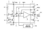
図1は、実施の形態1の定電圧発生回路の構成を示す回路図である。図1に示すように、実施の形態1は、従来同様の定電圧発生回路にスイッチ手段61と、スイッチ手段61の開閉制御を行うスイッチ制御手段62とを設けたものである。スイッチ手段61は、基準電圧発生源1のカレントミラー回路を構成する第1および第2のPMOSトランジスタ11,12の各ゲート、すなわち基準電圧発生源1の出力端子となる出力ノード16と、負の電源ライン4との間に接続されている。
FIG. 1 is a circuit diagram showing a configuration of the constant voltage generation circuit according to the first embodiment. As shown in FIG. 1, in the first embodiment, a switch means 61 and a switch control means 62 for controlling opening and closing of the switch means 61 are provided in a constant voltage generation circuit similar to the conventional one. The switch means 61 includes gates of the first and
スイッチ制御手段62は、電源投入直後に瞬間的にスイッチ手段61を閉(オン)状態にする制御信号を出力する。それによって、スイッチ手段61は、電源投入直後の一定期間だけ閉状態となり、その後、開(オフ)状態となる。スイッチ手段61は、例えば、MOSトランジスタにより構成される。スイッチ制御手段62の構成については、後述する。 The switch control means 62 outputs a control signal for instantaneously closing (turning on) the switch means 61 immediately after the power is turned on. As a result, the switch means 61 is closed for a certain period immediately after the power is turned on, and then opened (off). The switch means 61 is composed of, for example, a MOS transistor. The configuration of the switch control means 62 will be described later.
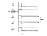
図2は、図1に示す定電圧発生回路の起動時の各部の電位変化を示す波形図である。図2(b)に示すように、スイッチ制御手段62の出力電位は、電源が投入されて負の電源ライン4の電位が負の電源電位VSSになる(図2(a))と同時に、スイッチ手段61を閉状態にする電位(図示例では、正の電源電位VDD)となる。その後、一定期間、例えば、システムクロックの1パルス分のような極めて短い期間が経過した後に、スイッチ制御手段62の出力電位は、スイッチ手段61を開状態にする電位(図示例では、負の電源電位VSS)となる。
FIG. 2 is a waveform diagram showing potential changes in various parts at the time of starting the constant voltage generating circuit shown in FIG. As shown in FIG. 2 (b), the output potential of the switch control means 62 is switched on at the same time when the power is turned on and the potential of the negative
図2(c)に示すように、第1の電位REF1は、スイッチ制御手段62の出力電位の変化に応じて、電源投入直後に、一時的に負の電源電位VSS側に引かれる。それによって、スイッチ手段61が閉状態となる。スイッチ手段61が閉じている間、第1のPMOSトランジスタ11のゲート電位および第2のPMOSトランジスタ12のゲート電位が負の電源電位VSS側に引かれるので、カレントミラー回路に流れる電流量が増える。その後、スイッチ制御手段62の出力電位がスイッチ手段61を開状態にする電位に変位する。これ以降、スイッチ手段61は開状態となる。それによって、第1の電位REF1は、徐々に正の電源電位VDD側へ変位し、電源投入から期間T2が経過した後に、一定電位で安定する。期間T2には、スイッチ手段61が閉(オン)状態の時間も含まれる。しかしながら、この時間は前述の通り極めて短いために、第1の電位REF1が安定する時間には影響しない。
As shown in FIG. 2C, the first potential REF1 is temporarily pulled to the negative power supply potential VSS side immediately after the power is turned on according to the change in the output potential of the switch control means 62. As a result, the switch means 61 is closed. While the switch means 61 is closed, the gate potential of the
同様に、第2の電位REF2は、図2(d)に示すように、一旦、負の電源電位VSS側に引かれた後、徐々に正の電源電位VDD側へ変位し、期間T2の経過後に、第1の電位REF1の安定電位と同じ電位で安定する。第1の電位REF1と第2の電位REF2とが同じ電位で安定した状態になると、図2(e)に示すように、レギュレート電圧VREGが安定した電位となる。つまり、レギュレート電圧VREGは、電源投入後、期間T2が経過した時点で安定する。この期間T2は、従来の期間T1に比べて極めて短く、例えば、室温で1ミリ秒程度であり、この値は低温でもほとんど変化しない。 Similarly, as shown in FIG. 2D, the second potential REF2 is once pulled to the negative power supply potential VSS side and then gradually displaced to the positive power supply potential VDD side, and the passage of the period T2 Later, the first potential REF1 is stabilized at the same potential as the stable potential. When the first potential REF1 and the second potential REF2 become stable at the same potential, the regulated voltage VREG becomes a stable potential as shown in FIG. 2 (e). That is, the regulated voltage VREG becomes stable when the period T2 has elapsed after the power is turned on. This period T2 is extremely shorter than the conventional period T1, for example, about 1 millisecond at room temperature, and this value hardly changes even at low temperatures.
上述したように、電源投入直後の一定期間、第1のPMOSトランジスタ11のゲート電位および第2のPMOSトランジスタ12のゲート電位は、スイッチ手段61およびスイッチ制御手段62により制御される。従って、スイッチ手段61およびスイッチ制御手段62は、ゲート制御手段としての機能を有する。また、スイッチ手段61とスイッチ制御手段62とは、電源投入直後の一定期間、基準電圧発生源1の出力端子となる出力ノード16を負の電源ライン4に接続するので、基準電圧制御手段としての機能を有する。
As described above, the gate potential of the
図3は、スイッチ制御手段62の第1の例を示す回路図である。図3に示すように、この第1の例は、抵抗63、コンデンサ64およびインバータ65により構成されている。抵抗63とコンデンサ64とは、正の電源電位VDDと負の電源電位VSSとの間に、直列に接続されている。インバータ65の入力端子は、抵抗63とコンデンサ64との接続ノード66に接続されている。インバータ65の出力端子67からは、スイッチ手段61の開閉を制御する制御信号が出力される。
FIG. 3 is a circuit diagram showing a first example of the switch control means 62. As shown in FIG. 3, the first example includes a
図4は、図3に示すスイッチ制御手段62の起動時の電位変化を示す波形図である。図4(b)に示すように、接続ノード66の電位は、電源が投入されて負の電源ライン4の電位が負の電源電位VSSになる(図4(a))と同時に、負の電源電位VSSとなる。その後、接続ノード66の電位は、徐々に正の電源電位VDD側へ変位する。
FIG. 4 is a waveform diagram showing a potential change when the switch control means 62 shown in FIG. 3 is activated. As shown in FIG. 4B, the potential of the
図4(c)に示すように、インバータ65の出力端子67の電位は、電源投入後、接続ノード66の電位が電源電圧の2分の1(VSS/2)に達するまでは正の電源電位VDDであり、接続ノード66の電位が電源電圧の2分の1(VSS/2)よりも正の電源電位VDD側になると、負の電源電位VSSになる。スイッチ手段61は、電源投入から、インバータ65の出力端子67の電位が正の電源電位VDDから負の電源電位VSSに反転するまでの期間T3の間、閉状態となる。
As shown in FIG. 4C, the potential of the
図5は、スイッチ制御手段62の第2の例を示す回路図である。図5に示すように、この第2の例は、発振回路68、発振停止検出回路69、バッファ70、抵抗71、コンデンサ72、インバータ73およびノア回路74により構成されている。発振回路68は、このスイッチ制御手段62を含むシステムのクロック信号75を出力する。発振停止検出回路69は、発振回路68に接続されており、発振回路68からのクロック信号75の出力が停止したこと、換言すれば、発振回路68が発振していることを検出する。
FIG. 5 is a circuit diagram showing a second example of the switch control means 62. As shown in FIG. 5, the second example includes an
バッファ70の入力端子は、発振停止検出回路69に接続されている。バッファ70の出力端子76は、ノア回路74の一方の入力端子に接続されている。また、バッファ70の出力端子76は、抵抗71の一端に接続されている。抵抗71の他端は、インバータ73の入力端子に接続されている。抵抗71とインバータ73との接続ノード77と、負の電源電位VSSとの間には、コンデンサ72が接続されている。インバータ73の出力端子は、ノア回路74のもう一方の入力端子に接続されている。ノア回路74の出力端子78からは、スイッチ手段61の開閉を制御する制御信号が出力される。
The input terminal of the
図6は、図5に示すスイッチ制御手段62の起動時の電位変化を示す波形図である。図6(b)に示すように、発振回路68は、電源が投入されて負の電源ライン4の電位が負の電源電位VSSになった(図6(a))後、しばらくしてから発振を開始し、クロック信号75を出力する。図6(c)に示すように、クロック信号75が出力されると、発振停止検出回路69から出力される検出信号の電位が反転し、バッファ70の出力端子76の電位が正の電源電位VDDから負の電源電位VSSになる。
FIG. 6 is a waveform diagram showing potential changes at the time of activation of the switch control means 62 shown in FIG. As shown in FIG. 6B, the
抵抗71およびコンデンサ72により遅延回路が構成されているため、図6(d)に示すように、抵抗71とインバータ73(コンデンサ72)との接続ノード77の電位は、バッファ70の出力端子76の電位変化から遅れて、正の電源電位VDDから徐々に負の電源電位VSSへ変位する。図6(e)に示すように、ノア回路74の出力端子78の電位は、電源投入後に負の電源電位VSSとなる。その後、発振回路68の発振が開始され、抵抗71とインバータ73との接続ノード77の電位が負の電源電位VSS側に引かれ始めると同時に、ノア回路74の出力端子78の電位は、正の電源電位VDDとなる。
Since the
そして、ノア回路74の出力端子78の電位は、接続ノード77の電位が電源電圧の2分の1(VSS/2)に達するまでは正の電源電位VDDのままであり、接続ノード77の電位が電源電圧の2分の1(VSS/2)よりも負の電源電位VSS側になると、負の電源電位VSSになる。つまり、スイッチ制御手段62からワンショットのパルスが発生する。スイッチ手段61は、このワンショットのパルスが発生している期間T4の間、閉状態となる。
The potential of the
実施の形態2.
図7は、実施の形態2の定電圧発生回路の構成を示す回路図である。図7に示すように、実施の形態2は、実施の形態1と同様のスイッチ手段61を第1および第2のPMOSトランジスタ11,12の各ゲート(出力ノード16)とレギュレート電圧出力端子35との間に設け、実施の形態1と同様のスイッチ制御手段62によりスイッチ手段61の開閉制御を行うものである。図7に示す定電圧発生回路の起動時の各部の電位変化は、実施の形態1と同じであり、その波形図は図2に示す通りである。
FIG. 7 is a circuit diagram showing a configuration of the constant voltage generation circuit according to the second embodiment. As shown in FIG. 7, in the second embodiment, the switch means 61 similar to that of the first embodiment is replaced with the gates (output nodes 16) of the first and
実施の形態2では、実施の形態1と同様に、スイッチ手段61およびスイッチ制御手段62は、ゲート制御手段としての機能を有する。また、スイッチ手段61とスイッチ制御手段62とは、電源投入直後の一定期間、基準電圧発生源1の出力端子となる出力ノード16をレギュレート電圧出力端子35に接続するので、基準電圧制御手段としての機能を有する。実施の形態2には、スイッチ手段61をMOSトランジスタで構成した場合に、そのMOSトランジスタがオフ状態であるときのリーク電流が実施の形態1よりも少ないという利点がある。その理由は、レギュレート電圧VREGが負の電源電位VSSよりも低いので、安定状態、すなわち、そのMOSトランジスタがオフ状態であるときのリーク電流が少ないためである。
In the second embodiment, as in the first embodiment, the switch means 61 and the switch control means 62 have a function as a gate control means. Further, the switch means 61 and the switch control means 62 connect the
実施の形態3.
図8は、実施の形態3の定電圧発生回路の構成を示す回路図である。図8に示すように、実施の形態3は、実施の形態1と同様のスイッチ手段61を差動アンプ2の二つの入力端子の間に設け、実施の形態1と同様のスイッチ制御手段62によりスイッチ手段61の開閉制御を行うものである。
FIG. 8 is a circuit diagram showing a configuration of the constant voltage generation circuit according to the third embodiment. As shown in FIG. 8, in the third embodiment, the switch means 61 similar to that in the first embodiment is provided between two input terminals of the
図9は、図8に示す定電圧発生回路の起動時の各部の電位変化を示す波形図である。図9(b)に示すように、スイッチ制御手段62の出力電位は、電源が投入されて負の電源ライン4の電位が負の電源電位VSSになる(図9(a))と同時に、スイッチ手段61を閉状態にする電位(図示例では、正の電源電位VDD)となる。その後、一定期間、例えば、システムクロックの1パルス分のような極めて短い期間が経過した後に、スイッチ制御手段62の出力電位は、スイッチ手段61を開状態にする電位(図示例では、負の電源電位VSS)となる。
FIG. 9 is a waveform diagram showing potential changes at various parts when the constant voltage generating circuit shown in FIG. 8 is started. As shown in FIG. 9 (b), the output potential of the switch control means 62 is switched on at the same time when the power is turned on and the potential of the negative
図9(c)に示すように、第1の電位REF1は、電源投入直後に、第2の電位REF2に引かれる。それによって、カレントミラー回路に流れる電流量が増える。そして、第1の電位REF1は、正の電源電位VDDから負の電源電位VSS側に急速に変位して、電源投入から期間T5が経過した後に、一定電位で安定する。一方、図9(d)に示すように、第2の電位REF2は、電源投入直後に、一旦、負の電源電位VSS側に引かれた後、急速に正の電源電位VDD側へ変位し、期間T5の経過後に、第1の電位REF1の安定電位と同じ電位で安定する。スイッチ手段61は、電源投入から期間T5が経過するまでは閉状態となり、期間T5の経過後は開状態となる。 As shown in FIG. 9C, the first potential REF1 is pulled to the second potential REF2 immediately after the power is turned on. As a result, the amount of current flowing through the current mirror circuit increases. Then, the first potential REF1 is rapidly displaced from the positive power supply potential VDD toward the negative power supply potential VSS, and is stabilized at a constant potential after a period T5 has elapsed since the power was turned on. On the other hand, as shown in FIG. 9D, the second potential REF2 is once pulled to the negative power supply potential VSS immediately after the power is turned on, and then rapidly displaced to the positive power supply potential VDD side. After the elapse of the period T5, the output voltage is stabilized at the same potential as that of the first potential REF1. The switch means 61 is in a closed state until the period T5 has elapsed since the power was turned on, and is in an open state after the period T5 has elapsed.
第1の電位REF1と第2の電位REF2とが同じ電位で安定した状態になると、図9(e)に示すように、レギュレート電圧VREGが安定した電位となる。つまり、レギュレート電圧VREGは、電源投入後、期間T5が経過した時点で安定する。この期間T5は、従来の期間T1に比べて極めて短く、例えば、室温で1ミリ秒程度であり、この値は、低温でもほとんど変化しない。 When the first potential REF1 and the second potential REF2 become stable at the same potential, the regulated voltage VREG becomes a stable potential as shown in FIG. 9 (e). That is, the regulated voltage VREG becomes stable when the period T5 elapses after the power is turned on. This period T5 is extremely shorter than the conventional period T1, for example, about 1 millisecond at room temperature, and this value hardly changes even at low temperatures.
実施の形態3では、実施の形態1と同様に、スイッチ手段61およびスイッチ制御手段62は、ゲート制御手段としての機能を有する。また、スイッチ手段61とスイッチ制御手段62とは、電源投入直後の一定期間、基準電圧発生源1の出力端子となる出力ノード16を差動アンプ2の、第2の電位REF2が入力される入力端子に接続するので、基準電圧制御手段としての機能を有する。
In the third embodiment, as in the first embodiment, the switch means 61 and the switch control means 62 have a function as a gate control means. The switch means 61 and the switch control means 62 are connected to the
実施の形態4.
図10は、実施の形態4の定電圧発生回路の構成を示す回路図である。図10に示すように、実施の形態4は、実施の形態1と同様のスイッチ手段61を第1および第2のNMOSトランジスタ13,14の各ゲート(基準電圧発生源1の前記出力ノード16と対をなすもう一つの出力ノード18)と正の電源ライン5との間に設け、実施の形態1と同様のスイッチ制御手段62によりスイッチ手段61の開閉制御を行うものである。実施の形態4では、電源投入直後に、基準電圧発生源1のもう一つの出力ノード18が、一時的に正の電源電位VDD側に引かれるので、第1および第2のNMOSトランジスタ13,14がオン状態となり、カレントミラー回路に流れる電流量が増える。
FIG. 10 is a circuit diagram showing a configuration of the constant voltage generation circuit according to the fourth embodiment. As shown in FIG. 10, in the fourth embodiment, the switch means 61 similar to that in the first embodiment is replaced with the gates of the first and
従って、図10に示す定電圧発生回路の起動時の各部の電位変化は、実施の形態1と同じであり、その波形図は図2に示す通りである。実施の形態4では、実施の形態1と同様に、スイッチ手段61およびスイッチ制御手段62は、ゲート制御手段としての機能を有する。また、スイッチ手段61とスイッチ制御手段62とは、電源投入直後の一定期間、基準電圧発生源1のもう一方の出力ノード18を正の電源ライン5に接続するので、基準電圧制御手段としての機能を有する。
Therefore, the potential change of each part at the time of starting the constant voltage generating circuit shown in FIG. 10 is the same as that of the first embodiment, and the waveform diagram thereof is as shown in FIG. In the fourth embodiment, as in the first embodiment, the
実施の形態5.
図11は、実施の形態5の定電圧発生回路の構成を示す回路図である。図11に示すように、実施の形態5は、実施の形態3において、スイッチ手段61をNMOSトランジスタ81で構成し、このNMOSトランジスタ81のオン状態とオフ状態との切り替えを定電圧発生回路内の信号により制御するようにしたものである。従って、実施の形態5では、スイッチ制御手段62は設けられていない。
FIG. 11 is a circuit diagram showing a configuration of the constant voltage generation circuit according to the fifth embodiment. As shown in FIG. 11, in the fifth embodiment, the switch means 61 is configured by an
NMOSトランジスタ81のゲートおよびドレインは、基準電圧発生源1の出力ノード16に接続されている。NMOSトランジスタ81のソースおよびバルクは、差動アンプ2の前記他方の入力端子に接続されている。つまり、NMOSトランジスタ81のゲートおよびドレインには、第1の電位REF1が印加され、そのソースおよびバルクには、第2の電位REF2が印加される。
The gate and drain of the
図12は、図11に示す定電圧発生回路の起動時の各部の電位変化を示す波形図である。図12(a)に示すように、電源が投入されて負の電源ライン4の電位が負の電源電位VSSになった時点では、図12(b)および(c)に示すように、第1の電位REF1と第2の電位REF2とには電位差が存在する。この電位差がある間、NMOSトランジスタ81がオン状態となり、第1の電位REF1が第2の電位REF2に引き下げられるので、カレントミラー回路に流れる電流量が増える。
FIG. 12 is a waveform diagram showing potential changes at various parts when the constant voltage generating circuit shown in FIG. 11 is started. As shown in FIG. 12A, when the power is turned on and the potential of the negative
そして、第1の電位REF1と第2の電位REF2とが同じ電位で安定した状態になると、図12(d)に示すように、レギュレート電圧VREGが安定した電位となる。この安定状態になるまでに要する時間は、従来の期間T1に比べて極めて短く、例えば、室温で1ミリ秒程度であり、低温で10ミリ秒程度である。また、安定状態になると、第1の電位REF1と第2の電位REF2とが同電位になるので、NMOSトランジスタ81はオフ状態となる。従って、貫通電流が流れたり、レギュレート電圧VREGに影響を及ぼすなどの不都合は、一切ない。
Then, when the first potential REF1 and the second potential REF2 become stable at the same potential, the regulated voltage VREG becomes a stable potential as shown in FIG. The time required to reach this stable state is extremely shorter than the conventional period T1, and is, for example, about 1 millisecond at room temperature and about 10 milliseconds at low temperature. In the stable state, the first potential REF1 and the second potential REF2 become the same potential, so that the
実施の形態5では、電源投入直後の一定期間、第1のPMOSトランジスタ11のゲート電位および第2のPMOSトランジスタ12のゲート電位は、NMOSトランジスタ81により制御される。従って、NMOSトランジスタ81は、ゲート制御手段としての機能を有する。また、NMOSトランジスタ81は、電源投入直後の一定期間、基準電圧発生源1の出力端子となる出力ノード16を差動アンプ2の、第2の電位REF2が入力される入力端子に接続するので、基準電圧制御手段としての機能を有する。
In the fifth embodiment, the gate potential of the
実施の形態6.
図13は、実施の形態6の定電圧発生回路の構成を示す回路図である。図13に示すように、実施の形態6は、実施の形態3において、スイッチ手段61をPMOSトランジスタ82で構成し、このPMOSトランジスタ82のオン状態とオフ状態との切り替えを定電圧発生回路内の信号により制御するようにしたものである。従って、実施の形態6では、スイッチ制御手段62は設けられていない。
Embodiment 6 FIG.
FIG. 13 is a circuit diagram showing a configuration of the constant voltage generation circuit of the sixth embodiment. As shown in FIG. 13, in the sixth embodiment, the switch means 61 is configured by a
PMOSトランジスタ82のソースは、基準電圧発生源1の出力ノード16に接続されている。PMOSトランジスタ82のゲートおよびドレインは、差動アンプ2の前記他方の入力端子に接続されている。バルクは、正の電源ライン5もしくは基準電圧発生源1の出力ノード16のどちらかに接続する。つまり、PMOSトランジスタ82のソースには、第1の電位REF1が印加され、そのゲートおよびドレインには、第2の電位REF2が印加され、そのバルクには、正の電源電位VDDもしくは第1の電位REF1が印加される。バルクを正の電源ライン5に接続し、VDDの電位にした場合、起動後は、PMOSトランジスタ82にバックゲートがかかるので、このトランジスタはONしにくくなる。PMOSトランジスタ82は、電源投入直後の一定期間のみオンさせたいので、役目を終えた起動後にオンしにくくなって都合がよい。後述する実施の形態7および8におけるPMOSトランジスタ83、84においても同様である。図13に示す定電圧発生回路の起動時の各部の電位変化は、実施の形態5と同じであり、その波形図は図12に示す通りである。
The source of the
実施の形態6では、電源投入直後の一定期間、第1のPMOSトランジスタ11のゲート電位および第2のPMOSトランジスタ12のゲート電位は、PMOSトランジスタ82により制御される。従って、PMOSトランジスタ82は、ゲート制御手段としての機能を有する。また、PMOSトランジスタ82は、電源投入直後の一定期間、基準電圧発生源1の出力端子となる出力ノード16を差動アンプ2の、第2の電位REF2が入力される入力端子に接続するので、基準電圧制御手段としての機能を有する。
In the sixth embodiment, the gate potential of the
実施の形態7.
図14は、実施の形態7の定電圧発生回路の構成を示す回路図である。図14に示すように、実施の形態7は、実施の形態1において、スイッチ手段61をPMOSトランジスタ83で構成し、このPMOSトランジスタ83のオン状態とオフ状態との切り替えを定電圧発生回路内の信号により制御するようにしたものである。従って、実施の形態7では、スイッチ制御手段62は設けられていない。
Embodiment 7 FIG.
FIG. 14 is a circuit diagram showing a configuration of the constant voltage generation circuit according to the seventh embodiment. As shown in FIG. 14, in the seventh embodiment, the switch means 61 is configured by a
PMOSトランジスタ83のソース、ゲートおよびドレインは、それぞれ、基準電圧発生源1の出力ノード16、差動アンプ2の前記他方の入力端子および負の電源ライン4に接続されている。なお、バルクは、正の電源ライン5もしくは基準電圧発生源1の出力ノード16のどちらかに接続する。つまり、PMOSトランジスタ83のソースには、第1の電位REF1が印加され、そのゲートには、第2の電位REF2が印加され、そのドレインには、負の電源電位VSSが印加され、そのバルクには、正の電源電位VDDもしくは第1の電位REF1が印加される。図14に示す定電圧発生回路の起動時の各部の電位変化は、実施の形態5と同じであり、その波形図は図12に示す通りである。
The source, gate, and drain of the
実施の形態7では、電源投入直後の一定期間、第1のPMOSトランジスタ11のゲート電位および第2のPMOSトランジスタ12のゲート電位は、PMOSトランジスタ83により制御される。従って、PMOSトランジスタ83は、ゲート制御手段としての機能を有する。また、PMOSトランジスタ83は、電源投入直後の一定期間、基準電圧発生源1の出力端子となる出力ノード16を負の電源ライン4に接続するので、基準電圧制御手段としての機能を有する。実施の形態7には、スイッチ手段61がNMOSトランジスタで構成されている場合に比べて、システムに接続される負荷への過電流などによって電源電圧に変動があった場合でも、その変動が第1の電位REF1に伝達されにくいという利点がある。
In the seventh embodiment, the gate potential of the
実施の形態8.
図15は、実施の形態8の定電圧発生回路の構成を示す回路図である。図15に示すように、実施の形態8は、実施の形態2において、スイッチ手段61をPMOSトランジスタ84で構成し、このPMOSトランジスタ84のオン状態とオフ状態との切り替えを定電圧発生回路内の信号により制御するようにしたものである。従って、実施の形態8では、スイッチ制御手段62は設けられていない。
Embodiment 8 FIG.
FIG. 15 is a circuit diagram showing a configuration of the constant voltage generation circuit according to the eighth embodiment. As shown in FIG. 15, in the eighth embodiment, the switch means 61 is configured by a
PMOSトランジスタ84のソース、ゲートおよびドレインは、それぞれ、基準電圧発生源1の出力ノード16、差動アンプ2の前記他方の入力端子およびレギュレート電圧出力端子35に接続されている。バルクは、正の電源ライン5もしくは基準電圧発生源1の出力ノード16のどちらかに接続する。つまり、PMOSトランジスタ84のソースには、第1の電位REF1が印加され、そのゲートには、第2の電位REF2が印加され、そのドレインには、レギュレート電圧VREGの電位が印加され、そのバルクには、正の電源電位VDDもしくは第1の電位REF1が印加される。図15に示す定電圧発生回路の起動時の各部の電位変化は、実施の形態5と同じであり、その波形図は図12に示す通りである。
The source, gate, and drain of the
実施の形態8では、電源投入直後の一定期間、第1のPMOSトランジスタ11のゲート電位および第2のPMOSトランジスタ12のゲート電位は、PMOSトランジスタ84により制御される。従って、PMOSトランジスタ84は、ゲート制御手段としての機能を有する。また、PMOSトランジスタ84は、電源投入直後の一定期間、基準電圧発生源1の出力端子となる出力ノード16をレギュレート電圧出力端子35に接続するので、基準電圧制御手段としての機能を有する。実施の形態8には、レギュレート電圧VREGが負の電源電位VSSよりも低いので、安定状態、すなわちPMOSトランジスタ84がオフ状態であるときのPMOSトランジスタ84のリーク電流が、実施の形態7のPMOSトランジスタ83のリーク電流よりも少ないという利点がある。
In the eighth embodiment, the
以上説明したように、各実施の形態によれば、電源を投入した後、短時間で基準電圧発生源1の出力電位REF1が所望の電位で安定するので、直ちに所望の安定したレギュレート電圧VREGが出力されるという効果を奏する。また、基準電圧発生源1の出力端子となる出力ノード16と負の電源ライン4との間にコンデンサが接続されないので、基準電圧発生源1の出力が電源変動の影響を受けずに済む。従って、レギュレート電圧VREGが安定するという効果を奏する。また、各実施の形態は、電源電圧が例えば3V程度であり、その半分程度のレギュレート電圧VREGで駆動される、低消費電力の小型電子機器の定電圧発生回路として有効であり、例えば時計に内蔵される定電圧発生回路に用いられる。
As described above, according to each embodiment, since the output potential REF1 of the reference
以上において、本発明は、上述した実施の形態に限らず、種々変更可能である。例えば、定電圧発生回路の基本的な構成は、図16に示す構成に限らない。スイッチ手段61は、MOSトランジスタに限らない。また、スイッチ制御手段62は、図3〜図6に示す構成に限らない。 As described above, the present invention is not limited to the above-described embodiment, and various modifications can be made. For example, the basic configuration of the constant voltage generation circuit is not limited to the configuration shown in FIG. The switch means 61 is not limited to a MOS transistor. Moreover, the switch control means 62 is not restricted to the structure shown in FIGS.
以上のように、本発明にかかる定電圧発生回路は、電源電圧を降圧したレギュレート電圧で駆動される小型電子機器に有用であり、特に、例えばソーラー時計を含む時計全般に適している。 As described above, the constant voltage generation circuit according to the present invention is useful for small electronic devices driven by a regulated voltage obtained by stepping down the power supply voltage, and is particularly suitable for all timepieces including solar timepieces, for example.
VDD 正の電源電位
VREG レギュレート電圧
VSS 負の電源電位
1 基準電圧発生源
2 差動アンプ
4 負の電源ライン
5 正の電源ライン
11,12,13,14 カレントミラー回路を構成するトランジスタ
16 基準電圧発生源の出力端子となる出力ノード
35 レギュレート電圧出力端子
61 スイッチ手段、ゲート制御手段、基準電圧制御手段
62 スイッチ制御手段、ゲート制御手段、基準電圧制御手段
81,82,83,84 スイッチ手段となるトランジスタ
VDD Positive power supply potential VREG Regulated voltage VSS Negative
Claims (8)
電源電圧に基づいて、レギュレート電圧を生成するための基準電圧を発生する基準電圧発生源と、A reference voltage generation source for generating a reference voltage for generating a regulated voltage based on the power supply voltage;
一方の入力端子に前記基準電圧発生源の出力電位が入力され、他方の入力端子に、レギュレート電圧出力端子の電位に所定の電位差を加算した電位が入力され、前記レギュレート電圧出力端子の電位を、前記2つの入力端子に入力される電位に基づいて一定に保つように動作する差動アンプと、The output potential of the reference voltage generation source is input to one input terminal, the potential obtained by adding a predetermined potential difference to the potential of the regulated voltage output terminal is input to the other input terminal, and the potential of the regulated voltage output terminal A differential amplifier that operates to keep constant based on the potential input to the two input terminals;
電源投入直後の一定期間、前記基準電圧発生源の出力端子の電流量が増えるように前記基準電圧発生源の出力電位を制御する基準電圧制御手段と、A reference voltage control means for controlling the output potential of the reference voltage generation source so that the amount of current at the output terminal of the reference voltage generation source increases for a certain period immediately after power-on;
を備えることを特徴とする定電圧発生回路。A constant voltage generation circuit comprising:
前記基準電圧制御手段は、前記カレントミラー回路を構成するトランジスタのゲートの電位を制御して前記カレントミラー回路に流れる電流量が増えるようにすることを特徴とする請求項1〜7のいずれか1つに記載の定電圧発生回路。8. The reference voltage control unit according to claim 1, wherein the reference voltage control unit controls a potential of a gate of a transistor constituting the current mirror circuit to increase an amount of current flowing through the current mirror circuit. Constant voltage generator circuit as described in 1.
Priority Applications (6)
| Application Number | Priority Date | Filing Date | Title |
|---|---|---|---|
| JP2004285925A JP4627651B2 (en) | 2004-09-30 | 2004-09-30 | Constant voltage generator |
| EP05788196A EP1798627B1 (en) | 2004-09-30 | 2005-09-29 | Constant voltage generating circuit |
| US11/663,997 US7560980B2 (en) | 2004-09-30 | 2005-09-29 | Constant voltage generating circuit |
| PCT/JP2005/018014 WO2006035898A1 (en) | 2004-09-30 | 2005-09-29 | Constant voltage generating circuit |
| DE602005016287T DE602005016287D1 (en) | 2004-09-30 | 2005-09-29 | CONSTANT VOLTAGE GENERATION CIRCUIT |
| CNB2005800329925A CN100476678C (en) | 2004-09-30 | 2005-09-29 | Constant voltage generating circuit |
Applications Claiming Priority (1)
| Application Number | Priority Date | Filing Date | Title |
|---|---|---|---|
| JP2004285925A JP4627651B2 (en) | 2004-09-30 | 2004-09-30 | Constant voltage generator |
Publications (3)
| Publication Number | Publication Date |
|---|---|
| JP2006099507A JP2006099507A (en) | 2006-04-13 |
| JP2006099507A5 JP2006099507A5 (en) | 2007-11-15 |
| JP4627651B2 true JP4627651B2 (en) | 2011-02-09 |
Family
ID=36119044
Family Applications (1)
| Application Number | Title | Priority Date | Filing Date |
|---|---|---|---|
| JP2004285925A Active JP4627651B2 (en) | 2004-09-30 | 2004-09-30 | Constant voltage generator |
Country Status (6)
| Country | Link |
|---|---|
| US (1) | US7560980B2 (en) |
| EP (1) | EP1798627B1 (en) |
| JP (1) | JP4627651B2 (en) |
| CN (1) | CN100476678C (en) |
| DE (1) | DE602005016287D1 (en) |
| WO (1) | WO2006035898A1 (en) |
Families Citing this family (6)
| Publication number | Priority date | Publication date | Assignee | Title |
|---|---|---|---|---|
| JP5426220B2 (en) * | 2009-04-13 | 2014-02-26 | 株式会社東芝 | Power supply noise elimination circuit |
| JP2013051858A (en) * | 2011-08-31 | 2013-03-14 | Toshiba Corp | Constant-voltage power-supply circuit and semiconductor integrated circuit |
| JP6083269B2 (en) * | 2013-03-18 | 2017-02-22 | 株式会社ソシオネクスト | Power supply circuit and semiconductor device |
| JP5983552B2 (en) * | 2013-07-19 | 2016-08-31 | 株式会社デンソー | Constant current constant voltage circuit |
| JP6320273B2 (en) * | 2014-10-27 | 2018-05-09 | 三菱電機株式会社 | Driving circuit |
| EP4254127A1 (en) * | 2022-03-29 | 2023-10-04 | Imec VZW | A voltage reference circuit and a power management unit |
Citations (5)
| Publication number | Priority date | Publication date | Assignee | Title |
|---|---|---|---|---|
| JP2594470Y2 (en) * | 1992-04-24 | 1999-04-26 | シチズン時計株式会社 | Reference voltage generation circuit |
| JP2000075947A (en) * | 1998-09-03 | 2000-03-14 | Toshiba Corp | Constant-voltage generating circuit |
| JP2001042960A (en) * | 1999-06-22 | 2001-02-16 | Alcatel | Monitor means and reference voltage generator having start-up means |
| JP2003051187A (en) * | 2001-06-29 | 2003-02-21 | Hynix Semiconductor Inc | Internal power voltage generator |
| JP3561716B1 (en) * | 2003-05-30 | 2004-09-02 | 沖電気工業株式会社 | Constant voltage circuit |
Family Cites Families (22)
| Publication number | Priority date | Publication date | Assignee | Title |
|---|---|---|---|---|
| CN85104092A (en) * | 1985-05-23 | 1987-03-04 | 中国科学院东海研究站 | Numerical regulated power supply |
| US4857823A (en) * | 1988-09-22 | 1989-08-15 | Ncr Corporation | Bandgap voltage reference including a process and temperature insensitive start-up circuit and power-down capability |
| JPH03288217A (en) * | 1990-04-03 | 1991-12-18 | Mitsubishi Electric Corp | Semiconductor integrated circuit device |
| JP3118929B2 (en) | 1992-01-27 | 2000-12-18 | 松下電工株式会社 | Constant voltage circuit |
| JP3149992B2 (en) | 1992-08-06 | 2001-03-26 | 日本電気アイシーマイコンシステム株式会社 | Semiconductor integrated circuit |
| KR970010284B1 (en) * | 1993-12-18 | 1997-06-23 | Samsung Electronics Co Ltd | Internal voltage generator of semiconductor integrated circuit |
| JPH07250437A (en) * | 1994-03-09 | 1995-09-26 | Canon Inc | Solar battery power supply |
| KR0143344B1 (en) * | 1994-11-02 | 1998-08-17 | 김주용 | Reference voltage generator |
| JPH09265329A (en) | 1996-03-27 | 1997-10-07 | New Japan Radio Co Ltd | Bias generation circuit and regulator circuit |
| JP3185698B2 (en) * | 1997-02-20 | 2001-07-11 | 日本電気株式会社 | Reference voltage generation circuit |
| KR100240874B1 (en) * | 1997-03-18 | 2000-01-15 | 윤종용 | A circuit of generating internal voltage of semiconductor device |
| CN2374879Y (en) * | 1999-04-23 | 2000-04-19 | 乐清市长城电源有限公司 | A. C. automatic voltage regulator without spacing loss |
| JP3423282B2 (en) | 2000-10-18 | 2003-07-07 | 株式会社 沖マイクロデザイン | Semiconductor integrated circuit |
| DE10237122B4 (en) * | 2002-08-13 | 2011-06-22 | Infineon Technologies AG, 81669 | Circuit and method for setting the operating point of a BGR circuit |
| US6677808B1 (en) * | 2002-08-16 | 2004-01-13 | National Semiconductor Corporation | CMOS adjustable bandgap reference with low power and low voltage performance |
| US6815941B2 (en) * | 2003-02-05 | 2004-11-09 | United Memories, Inc. | Bandgap reference circuit |
| US6784652B1 (en) * | 2003-02-25 | 2004-08-31 | National Semiconductor Corporation | Startup circuit for bandgap voltage reference generator |
| KR100626367B1 (en) * | 2003-10-02 | 2006-09-20 | 삼성전자주식회사 | Internal voltage generator |
| JP4150326B2 (en) * | 2003-11-12 | 2008-09-17 | 株式会社リコー | Constant voltage circuit |
| US7113025B2 (en) * | 2004-04-16 | 2006-09-26 | Raum Technology Corp. | Low-voltage bandgap voltage reference circuit |
| KR101056737B1 (en) * | 2004-09-20 | 2011-08-16 | 삼성전자주식회사 | Device that generates internal power voltage |
| US7321256B1 (en) * | 2005-10-18 | 2008-01-22 | Xilinx, Inc. | Highly reliable and zero static current start-up circuits |
-
2004
- 2004-09-30 JP JP2004285925A patent/JP4627651B2/en active Active
-
2005
- 2005-09-29 EP EP05788196A patent/EP1798627B1/en active Active
- 2005-09-29 US US11/663,997 patent/US7560980B2/en active Active
- 2005-09-29 DE DE602005016287T patent/DE602005016287D1/en active Active
- 2005-09-29 CN CNB2005800329925A patent/CN100476678C/en active Active
- 2005-09-29 WO PCT/JP2005/018014 patent/WO2006035898A1/en active Application Filing
Patent Citations (5)
| Publication number | Priority date | Publication date | Assignee | Title |
|---|---|---|---|---|
| JP2594470Y2 (en) * | 1992-04-24 | 1999-04-26 | シチズン時計株式会社 | Reference voltage generation circuit |
| JP2000075947A (en) * | 1998-09-03 | 2000-03-14 | Toshiba Corp | Constant-voltage generating circuit |
| JP2001042960A (en) * | 1999-06-22 | 2001-02-16 | Alcatel | Monitor means and reference voltage generator having start-up means |
| JP2003051187A (en) * | 2001-06-29 | 2003-02-21 | Hynix Semiconductor Inc | Internal power voltage generator |
| JP3561716B1 (en) * | 2003-05-30 | 2004-09-02 | 沖電気工業株式会社 | Constant voltage circuit |
Also Published As
| Publication number | Publication date |
|---|---|
| EP1798627B1 (en) | 2009-08-26 |
| EP1798627A4 (en) | 2008-04-02 |
| EP1798627A1 (en) | 2007-06-20 |
| JP2006099507A (en) | 2006-04-13 |
| WO2006035898A1 (en) | 2006-04-06 |
| US20080018386A1 (en) | 2008-01-24 |
| US7560980B2 (en) | 2009-07-14 |
| CN101031855A (en) | 2007-09-05 |
| CN100476678C (en) | 2009-04-08 |
| DE602005016287D1 (en) | 2009-10-08 |
Similar Documents
| Publication | Publication Date | Title |
|---|---|---|
| KR102509824B1 (en) | Oscillator | |
| US20220294426A1 (en) | Ultra-low energy per cycle oscillator topology | |
| JP5225876B2 (en) | Power-on reset circuit | |
| EP1378995A2 (en) | Oscillation circuit, constant voltage generation circuit, semiconductor device, electronic equipment and timepiece | |
| JP2001147725A (en) | Bandgap reference circuit | |
| TWI732904B (en) | Compensation device for compensating pvt variations of an analog and/or digital circuit | |
| JP2013504263A (en) | Temperature compensated RC oscillator for signal processing ASIC using MOSFET source bulk voltage | |
| JP3751785B2 (en) | Bias circuit for semiconductor integrated circuit | |
| US7560980B2 (en) | Constant voltage generating circuit | |
| JPS6242283B2 (en) | ||
| JPH04229313A (en) | Buffer circuit | |
| US7102439B2 (en) | Low voltage differential amplifier circuit and a sampled low power bias control technique enabling accommodation of an increased range of input levels | |
| TWI249285B (en) | Low voltage differential amplifier circuit and bias control technique enabling accommodation of an increased range of input levels | |
| JP3561716B1 (en) | Constant voltage circuit | |
| JP3262079B2 (en) | Reference voltage generation circuit | |
| JP2021153259A (en) | Discharge control circuit and current source circuit | |
| US6198344B1 (en) | Back bias voltage level sensing circuit | |
| US11836001B2 (en) | Circuit device and real-time clock device | |
| KR100488584B1 (en) | Power-on reset circuit | |
| JPS6036644B2 (en) | oscillation circuit | |
| JPH0697732A (en) | Oscillation circuit | |
| JP2004295705A (en) | Constant voltage power supply circuit and electronic clock using it | |
| JP2003084085A (en) | Electronic timepiece | |
| GB1602371A (en) | Amplitude control inverter circuit for electronic device | |
| JP2008244787A (en) | Oscillation suspension detecting circuit, oscillator unit, semiconductor device, electronic equipment, and clock |
Legal Events
| Date | Code | Title | Description |
|---|---|---|---|
| A521 | Request for written amendment filed |
Free format text: JAPANESE INTERMEDIATE CODE: A523 Effective date: 20070928 |
|
| A621 | Written request for application examination |
Free format text: JAPANESE INTERMEDIATE CODE: A621 Effective date: 20070928 |
|
| TRDD | Decision of grant or rejection written | ||
| A01 | Written decision to grant a patent or to grant a registration (utility model) |
Free format text: JAPANESE INTERMEDIATE CODE: A01 Effective date: 20101102 |
|
| A01 | Written decision to grant a patent or to grant a registration (utility model) |
Free format text: JAPANESE INTERMEDIATE CODE: A01 |
|
| A61 | First payment of annual fees (during grant procedure) |
Free format text: JAPANESE INTERMEDIATE CODE: A61 Effective date: 20101108 |
|
| FPAY | Renewal fee payment (event date is renewal date of database) |
Free format text: PAYMENT UNTIL: 20131119 Year of fee payment: 3 |
|
| R150 | Certificate of patent or registration of utility model |
Ref document number: 4627651 Country of ref document: JP Free format text: JAPANESE INTERMEDIATE CODE: R150 Free format text: JAPANESE INTERMEDIATE CODE: R150 |
|
| S533 | Written request for registration of change of name |
Free format text: JAPANESE INTERMEDIATE CODE: R313533 |
|
| R350 | Written notification of registration of transfer |
Free format text: JAPANESE INTERMEDIATE CODE: R350 |
|
| R250 | Receipt of annual fees |
Free format text: JAPANESE INTERMEDIATE CODE: R250 |
|
| R250 | Receipt of annual fees |
Free format text: JAPANESE INTERMEDIATE CODE: R250 |
|
| R250 | Receipt of annual fees |
Free format text: JAPANESE INTERMEDIATE CODE: R250 |