JP4612848B2 - Imaging apparatus and control method thereof - Google Patents
Imaging apparatus and control method thereof Download PDFInfo
- Publication number
- JP4612848B2 JP4612848B2 JP2005039522A JP2005039522A JP4612848B2 JP 4612848 B2 JP4612848 B2 JP 4612848B2 JP 2005039522 A JP2005039522 A JP 2005039522A JP 2005039522 A JP2005039522 A JP 2005039522A JP 4612848 B2 JP4612848 B2 JP 4612848B2
- Authority
- JP
- Japan
- Prior art keywords
- offset correction
- signal
- region
- correction value
- read
- Prior art date
- Legal status (The legal status is an assumption and is not a legal conclusion. Google has not performed a legal analysis and makes no representation as to the accuracy of the status listed.)
- Expired - Fee Related
Links
Images


Description
本発明は、CCDやCMOSイメージセンサ等の撮像素子を用いた撮像装置及びその制御方法に関する。 The present invention relates to an imaging apparatus using an imaging element such as a CCD or a CMOS image sensor, and a control method thereof.
従来、CCDやCMOSイメージセンサ等の撮像素子を使用したデジタルカメラやビデオカメラ等の撮像装置が普及している。 2. Description of the Related Art Conventionally, imaging devices such as digital cameras and video cameras using imaging elements such as CCDs and CMOS image sensors have become widespread.
図6は、従来のデジタルカメラやデジタルビデオカメラの構成を示すブロック図で、101は撮像素子であり、一般的にはCCDまたはCMOSセンサが使用される。102は撮像素子101からのアナログ信号をデジタル信号に変換するA/D変換器である。103はDSP(DigitalSignalProseccer)であり、A/D変換器102からのデータに対して各種補正処理及び現像処理を行う。またDSP103では、ROM106、RAM107等の各種メモリの制御、記録媒体108への画像データの書き込み処理が行われる。
FIG. 6 is a block diagram showing the configuration of a conventional digital camera or digital video camera.
104は、撮像素子101、A/D変換器102、DSP103にクロック信号や制御信号を供給するタイミング発生回路であり、CPU105により制御される。105はDSP103、タイミング発生回路104の制御、及び測光、測距など不図示の各部を使ったカメラ機能の制御を行うCPUである。後述するスイッチ109〜111、モードダイアル112が接続され、それぞれの状態に応じた処理を実行する。
A
106はCPU105で実行されるカメラの制御プログラムやDSP103で用いる各種補正データを記憶するROM、107はDSP103で処理される画像データや補正データを一時的に記憶するRAMである。RAM107はROM106より高速のアクセスが可能である。108は撮影された画像を保存するコンパクトフラッシュ(登録商標)カード等の記録媒体であり、不図示のコネクタを介してカメラと接続される。
A
109はカメラを起動させるための電源スイッチ(SW)、110は、不図示のシャッターボタンの第1の所定動作(例えば半押し)によりONとなり、測光処理、測距処理等の動作開始を指示するシャッタースイッチSW1、111は、不図示のシャッターボタンの第2の所定動作(例えば全押し)によりONとなり、不図示のミラー及びシャッターを駆動し、撮像素子101から読み出した信号をA/D変換器102、DSP103を介して記録媒体108に書き込む一連の撮像動作の開始を指示するシャッタースイッチSW2である。
図7は、図6に示す構成を有する撮像装置の制御を示したフローチャートである。まず、ステップS101でカメラを起動する電源SW109がONされているか否か判定し、OFFならステップS101を繰り返す。ここで電源SW109がONされていれば、ステップS102でモードダイアル112が撮影モードに設定されているか否かを判別する。その他のモードに設定されていればステップS103で選択されているモードに応じた処理を行ってからステップS101へ戻り、撮影モードに設定されていればステップS104へ進む。
FIG. 7 is a flowchart showing control of the imaging apparatus having the configuration shown in FIG. First, in step S101, it is determined whether or not the
ステップS104では、シャッタースイッチSW1(110)がONしているか否か判定する。SW1(110)がOFFである場合、ステップS101に戻って、上述した処理を繰り返し、SW1(110)がONである場合には、ステップS105に進む。 In step S104, it is determined whether the shutter switch SW1 (110) is ON. If SW1 (110) is OFF, the process returns to step S101 and the above-described processing is repeated. If SW1 (110) is ON, the process proceeds to step S105.
ステップS105では、不図示の測光制御部及び測距制御部を用いて、絞り値およびシャッター速度を決定する測光処理、撮影レンズ焦点を被写体に合わせる測距処理が行われる。 In step S105, using a photometry control unit and a distance measurement control unit (not shown), photometry processing for determining the aperture value and shutter speed and distance measurement processing for adjusting the photographing lens focus to the subject are performed.
ステップS105の測光・測距処理が終了すると、続くステップS106でシャッタースイッチSW2(111)の状態を判定する。SW2がOFFである場合にはステップS104に戻って上述した処理を繰り返し、ONである場合にはステップS107で撮影処理が実行される。なお、この撮影処理の詳細については後述する。 When the photometry / ranging process in step S105 is completed, the state of the shutter switch SW2 (111) is determined in a subsequent step S106. If SW2 is OFF, the process returns to step S104 and the above-described processing is repeated. If SW2 is ON, shooting processing is executed in step S107. Details of this photographing process will be described later.
ステップS107の撮影処理が終了するとステップS108へ進み、撮影した画像データに対し、DSP103で現像処理を行う。続いてステップS109で、現像処理の終了した画像データに対し圧縮処理を行って、圧縮した画像データをRAM107の空き領域に格納する。
When the photographing process in step S107 is completed, the process proceeds to step S108, and the DSP 103 performs development processing on the photographed image data. In step S109, the image data that has undergone development processing is subjected to compression processing, and the compressed image data is stored in an empty area of the
ステップS110では、RAM107に格納されている画像データを読み出して、記録媒体108への記録処理を実行する。記録処理終了後、ステップS101へ戻り、次の処理に備える。
In step S110, the image data stored in the
次に、ステップS107で行われる撮影処理動作の詳細について図8を参照して説明する。 Next, details of the photographing processing operation performed in step S107 will be described with reference to FIG.
まずステップS201でミラーをミラーアップ位置に移動させ、ステップS202で、図7のステップS105の測光処理で得られた測光データに基づいて、所定の絞り値まで絞りを駆動する。ステップS203で撮像素子101の電荷クリア動作を行い、ステップS204で電荷蓄積を開始する。電荷蓄積開始後、ステップS205でシャッターを開き、撮像素子101の露光を開始する(ステップS206)。
First, in step S201, the mirror is moved to the mirror up position, and in step S202, the aperture is driven to a predetermined aperture value based on the photometric data obtained by the photometric processing in step S105 of FIG. In step S203, the charge clear operation of the
その後、ステップS207で測光データに従って露光終了まで待ち、ステップS208でシャッターを閉じる。ステップS309で開放の絞り値まで絞りを駆動し、ステップS210ではミラーダウン位置までミラーを駆動する。ステップS211では設定した電荷蓄積時間が経過するまで待ち、撮像素子101の電荷蓄積を終了する(ステップS212)。最後にステップS213で撮像素子101の信号が読み出され、一連の処理を終了してメインの処理へ復帰する。
Thereafter, in step S207, the process waits for the end of exposure according to the photometric data, and the shutter is closed in step S208. In step S309, the aperture is driven to the open aperture value, and in step S210, the mirror is driven to the mirror down position. In step S211, the process waits until the set charge accumulation time elapses, and ends the charge accumulation of the image sensor 101 (step S212). Finally, in step S213, the signal of the
以上が一連のカメラ動作の説明である。 The above is a description of a series of camera operations.
また、撮像素子を使用した撮像装置においては、信号の読出し時間を短縮し連写速度を上げるため、複数の読出しライン(チャンネル)を用いる方法が一般的に知られている。図9に撮像素子101を複数チャンネル(ここでは2チャンネル)で構成した例を示す。401a,401b,403a,403bはいずれも撮像素子101を構成する画素であり、図のように格子状に配置されている。これらの画素には、それぞれR、G、Bいずれかの色フィルタが載っており、例えば、水平方向にRGを繰り返す行とGBを繰り返す行を垂直方向に交互に繰り返すように色フィルタが配置されている。402a,402b,404a,404bはスイッチであり、各列の画素信号を読出しライン405a,405bに転送する。406a,406bは読出しライン405a,405bに転送された画素信号を増幅して出力するためのアンプである。
In an imaging apparatus using an imaging element, a method using a plurality of readout lines (channels) is generally known in order to shorten a signal readout time and increase a continuous shooting speed. FIG. 9 shows an example in which the
上記構成を有する撮像素子101では、画素信号の読出しは1行ずつ順に行われる。まず、スイッチ402a,402bがONされ、画素401a、401bの信号が読出しライン405a,405bを介してアンプ406a,406bへそれぞれ転送される。続いてスイッチ404a,404bがONされ、画素403a,403bの信号が読み出しライン405a,405bに転送され、先ほどと同様にアンプ406a,406bを通して出力される。このような繰り返しにより1行分の画素信号を読み出し終えると、同様に次の行の信号を順に読みだす。
In the
このように複数の読出しライン(チャンネル)を用いる場合には、チャンネル数分の画素を同時に読み出すことができるため、信号読出し時間を短縮し連写速度を上げることが可能となる。 When a plurality of readout lines (channels) are used in this way, pixels corresponding to the number of channels can be read out simultaneously, so that the signal readout time can be shortened and the continuous shooting speed can be increased.
また、上記撮像素子においては、暗電流成分を除去してダークオフセットレベルを所望の出力レベルに合わせ込むために、オフセットクランプ処理が行われるのが一般的である。このオフセットクランプ処理の回路は、センサ内部、或いは撮像素子の出力信号をアナログ−デジタル変換するA/D変換器などに設けられる。 Further, in the image pickup device, an offset clamp process is generally performed in order to remove the dark current component and adjust the dark offset level to a desired output level. This offset clamp processing circuit is provided in the sensor or in an A / D converter for analog-digital conversion of the output signal of the image sensor.
上記のような複数チャンネル構成の撮像装置においては、回路オフセットの違いによってチャンネル毎にダークレベルが異なるチャンネル間オフセットが発生することがある。チャンネル間オフセットは、ノイズとして撮影画像の画質を劣化させると共に、ホワイトバランス演算を誤らせる原因ともなる。 In an imaging apparatus having a multi-channel configuration as described above, an offset between channels with different dark levels may occur for each channel due to a difference in circuit offset. The channel-to-channel offset deteriorates the image quality of the captured image as noise and causes a white balance calculation to be erroneous.
こうした回路オフセット成分の除去と画素暗電流成分の除去を目的として、オフセットクランプ回路が設けられるものもある(例えば、特許文献1参照)。 In some cases, an offset clamp circuit is provided for the purpose of removing such circuit offset components and pixel dark current components (see, for example, Patent Document 1).
この特許文献1では、OB部が撮像素子の有効画素部(撮影画像の画像信号として利用する画素の領域)の左右領域に設けられており、各ライン毎に取得したOB部の画素値を用いて黒レベルの補正を行う。 In Patent Document 1, the OB portion is provided in the left and right regions of the effective pixel portion (the pixel region used as the image signal of the captured image) of the image sensor, and the pixel value of the OB portion obtained for each line is used. To correct the black level.
チャンネル間オフセットは、時間の経過とともに温度や蓄積時間等の条件の変化に伴って変化することもあるので、撮影した画像データ毎にオフセット補正値を算出して補正するのが望ましい。しかしながら、オフセット補正値の算出には時間がかかるため、撮影時にリアルタイムで補正を行うことが難しいという問題があった。 Since the offset between channels may change with changes in conditions such as temperature and accumulation time as time passes, it is desirable to calculate and correct an offset correction value for each captured image data. However, since it takes time to calculate the offset correction value, there is a problem that it is difficult to perform correction in real time at the time of shooting.
例えば、上述した特許文献1の構成では、各ライン毎にOB部の画素値を用いてオフセット補正値を算出するため、補正値の算出速度が撮像素子の読み出し速度と比較して遅い撮像装置では、撮像素子の読み出し速度を算出速度に合わせて遅くしなければならず、撮像素子の読み出し速度を十分に生かすことができない。 For example, in the configuration of Patent Document 1 described above, since the offset correction value is calculated for each line using the pixel value of the OB portion, in an imaging apparatus in which the correction value calculation speed is slower than the reading speed of the image sensor. The reading speed of the image sensor must be slowed down in accordance with the calculated speed, and the reading speed of the image sensor cannot be fully utilized.
また、撮像素子から読み出した画素信号を、オフセット補正せずにOB部の信号も含めて一旦RAM107に書き込み、書き込んだ画素信号を再度読み出してオフセット補正する方法も考えられるが、この方法では、撮像素子の読み出し速度を上げることはできるものの、画素信号の書き込み及び読み込みに時間がかかるため、スループットにかかる時間は長くなってしまう。また、オフセット補正処理にかかる時間を短縮するために、過去に算出したオフセット補正値を用いて補正した場合には、温度変化、ノイズ、撮像素子の欠陥画素等の影響を受け、チャンネル間オフセットが発生してしまうことがある。
In addition, a method of writing the pixel signal read from the image sensor to the
本発明は上記問題点を鑑みてなされたものであり、撮像素子の読み出し速度をできるだけ落とすこと無く、温度・蓄積時間等の条件の変化にも対応した適切なオフセット補正をリアルタイムで行えるようにすることを目的とする。 The present invention has been made in view of the above-described problems, and enables appropriate offset correction corresponding to changes in conditions such as temperature and accumulation time in real time without reducing the readout speed of the image sensor as much as possible. For the purpose.
上記目的を達成するために、本発明の撮像装置は、複数の画素から構成され、オフセット補正の基準となる画素信号が読み出される第1領域と、画像信号として利用する画素信号が読み出される第2領域とを含む撮像素子と、前記撮像素子から画素信号を読み出すための駆動信号を発生する駆動信号発生手段と、前記第1領域の画素信号に基づいてオフセット補正値を算出する算出手段と、前記オフセット補正値を記憶する記憶手段と、前記記憶したオフセット補正値を用いて、前記第2領域から読み出される画素信号を補正するオフセット補正手段と、前記第1領域の画素信号の読み出し終了後に前記駆動信号発生手段が前記駆動信号の発生を停止するように制御し、読み出した前記第1領域の画素信号に基づいてオフセット補正値を前記算出手段が算出し、算出した前記オフセット補正値を前記記憶手段に記憶するように制御し、前記オフセット補正値の前記記憶手段への記憶後に、前記駆動信号発生手段が前記駆動信号の発生を再開して、前記第2領域の画素信号を読み出すように制御する制御手段とを有する。 In order to achieve the above object, an image pickup apparatus according to the present invention includes a first region in which a pixel signal serving as a reference for offset correction is read, and a second signal from which a pixel signal used as an image signal is read . An image pickup device including a region, a drive signal generation unit that generates a drive signal for reading a pixel signal from the image pickup device, a calculation unit that calculates an offset correction value based on the pixel signal of the first region, and offset correction Symbol value you store憶means, by using the offset correction value the storage, and an offset correcting means for correcting the pixel signal read from the second region, after the read end of the pixel signal of the first region said drive signal generating means is controlled to stop the generation of the drive signal, the offset correction value based on the pixel signals of the first region read the Detecting means calculates the calculated the offset correction value is controlled to be stored in the storage means, after storage in the memory means of the offset correction value, resuming generation of said drive signal generating means said drive signal to, and a control Gosuru control means to read out pixel signals of the second region.
また、複数の画素から構成され、オフセット補正の基準となる画素信号が読み出される第1領域と、画像信号として利用する画素信号が読み出される第2領域とを含む撮像素子と、前記撮像素子から画素信号を読み出すための駆動信号を発生する駆動信号発生手段とを有する撮像装置の本発明の制御方法は、前記第1領域の画素信号を読み出す第1読み出し工程と、前記第1領域の画素信号の読み出し終了後に前記駆動信号発生手段が前記駆動信号の発生を停止する駆動停止工程と、前記第1の領域の画素信号に基づいてオフセット補正値を算出する算出工程と、前記算出工程で算出した前記オフセット補正値を記憶手段に記憶する記憶工程と、前記記憶工程におけるオフセット補正値の前記記憶手段への記憶後に、前記駆動信号発生手段が前記駆動信号の発生を再開する駆動再開工程と、前記第2領域の画素信号を読み出す第2読み出し工程と、前記記憶したオフセット補正値を用いて、前記第2領域から読み出される画素信号を補正するオフセット補正工程とを有する。 Also, it is composed of a plurality of pixels, a first region where the pixel signal as a reference of the offset correction is read, and an image pickup element and a second region where the pixel signal to be used as the image signal is read out, the pixel from the image sensor The control method of the present invention for an imaging apparatus having a drive signal generating means for generating a drive signal for reading a signal includes a first readout step of reading out a pixel signal of the first region, and a pixel signal of the first region . a drive stop step of stopping the driving signal generating means generates the drive signal after the read end, a calculation step of calculating the offset correction value based on the picture element signal of the first region, calculated in the calculating step wherein the offset correction value storing means SL you stored in憶step, after storage in the memory means of the offset correction value in the storage step, said drive signal generating means Using serial resuming driving restart process the generation of driving signals, and a second reading step of reading the pixel signal of the second region, the offset correction value said storage, corrects the pixel signal read from the second region Offset correction step.
本発明によれば、撮像素子の読み出し速度をできるだけ落とすこと無く、温度・蓄積時間等の条件の変化にも対応した適切なオフセット補正をリアルタイムで行うことができる。 According to the present invention, appropriate offset correction corresponding to changes in conditions such as temperature and storage time can be performed in real time without reducing the readout speed of the image sensor as much as possible.
以下、添付図面を参照して本発明を実施するための最良の形態を詳細に説明する。 The best mode for carrying out the present invention will be described below in detail with reference to the accompanying drawings.
<第1の実施形態>
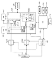
図1は、本発明の第1の実施形態における撮像装置の構成を示すブロック図である。なお、図6と同様の構成には同じ参照番号を付し、説明を省略する。図1において、508はOB部積分回路であり、A/D変換器102を介して撮像素子101から読み出される画素信号のうち、画素の遮光された部分(Optical Black、以下、「OB部」と呼ぶ。)の画素信号を積分する。また509はDSP103のオフセット補正部であり、減算器510及び補正値を保持するRAM511により構成される。オフセット補正部509を通った信号は、画像データの一時記憶用のRAM107に書き込まれる。
<First Embodiment>
FIG. 1 is a block diagram illustrating a configuration of an imaging apparatus according to the first embodiment of the present invention. In addition, the same reference number is attached | subjected to the structure similar to FIG. 6, and description is abbreviate | omitted. In FIG. 1,
上記構成を有する本第1の実施形態の撮像装置の基本動作は、図7及び図8を参照して説明したものと同様であるが、図8のステップS213で行われる撮像信号読み出し処理に特徴があるため、以下、その具体的な動作を図2のフローチャートを参照して説明する。 The basic operation of the imaging apparatus according to the first embodiment having the above-described configuration is the same as that described with reference to FIGS. 7 and 8, but is characterized by the imaging signal readout process performed in step S213 in FIG. Therefore, the specific operation will be described below with reference to the flowchart of FIG.
図8のステップS212までの動作で撮像素子101への電荷蓄積が終了すると、まずステップS301において、撮像素子101から画素信号を読み出すための駆動信号の出力を開始する。図3は、撮像素子101の画素領域を示した概念図であり、読み出しは撮像素子101の上側から1行ずつ行われる。この時点では、オフセット補正部509を通ってRAM107に書き込まれる画像データはオフセット成分を含んでいる。
When charge accumulation in the
読み出しが図3に示す積分開始行まで達すると、ステップS302でOB部の所定領域の信号の積分を開始する。この積分動作はDSP103のOB部積分回路508を用いて行われる。また、積分領域はレジスタ設定により予め設定しておくことができる。
When the reading reaches the integration start line shown in FIG. 3, integration of signals in a predetermined area of the OB portion is started in step S302. This integration operation is performed using the OB
続くステップS303では積分領域の画素信号が全て読み出されるまで動作を継続し、読み出しが積分領域の終了行に達し、積分領域が全て読み出されたら、ステップS304で積分動作を終了する。 In subsequent step S303, the operation is continued until all the pixel signals in the integration region are read out. When the readout reaches the end row of the integration region and all the integration regions are read out, the integration operation is ended in step S304.
積分終了後、ステップS305で撮像素子101の駆動信号を停止し、読み出し動作を中断する。読み出し中断後、ステップS306でDSP103はOB部積分回路508の積分結果からオフセット補正値の演算を行う。この補正値演算としては、例えば、積分結果からOB部の平均値を算出し、平均値と所望のダークレベルとの差分を取るといった方法が考えられる。勿論、本発明がオフセット補正値演算方法により制限されるものではないことは言うまでもなく、撮像装置の構成に適した方法によりオフセット補正値を算出すれば良い。
After the integration is completed, the drive signal for the
オフセット補正値を算出したら、ステップS307において、算出した補正値をオフセット補正部509のRAM511に設定し、続いてステップS308で駆動信号出力を再開し、撮像素子101の開口部(露光領域)を含む残り部分の読み出しを行う。ステップS308の読み出し再開以降に読み出される画素信号からは、RAM511に設定されたオフセット補正値を用いて減算器510によりでオフセット成分が除去され、RAM107に書き込まれることになる。
After calculating the offset correction value, in step S307, the calculated correction value is set in the
そしてステップS309にて撮像素子101の最終行まで駆動信号の出力を行い、撮像信号の読み出しを終了する。
In step S309, the drive signal is output up to the last row of the
図4は上述した撮像装置の読み出し動作のタイミングチャートである。 FIG. 4 is a timing chart of the reading operation of the imaging apparatus described above.
垂直同期信号、水平同期信号はDSP103からタイミング発生回路104に与えられる信号である。垂直同期信号は1画面の読み出し開始を指示し、水平同期信号は1行単位の時間を表す。
The vertical synchronization signal and the horizontal synchronization signal are signals given from the
垂直シフトレジスタ駆動信号は撮像素子101の選択行を切り換えていくための垂直シフトレジスタを駆動する信号であり、水平同期信号に基づいてタイミング発生回路104にて生成される。また、水平シフトレジスタ駆動信号は撮像素子101の各行を読み出す際に選択列を切り換えていくための水平シフトレジスタの駆動信号であり、水平同期信号に基づいてタイミング発生回路104にて生成される。
The vertical shift register drive signal is a signal for driving the vertical shift register for switching the selected row of the
図4に示すように、t1において図2のステップS304の読み出し開始と共にDSP103は垂直同期信号を出力すると共に、水平同期信号を一定周期で出力し始める。タイミング発生回路104は、水平同期信号に基づいて垂直、水平シフトレジスタ駆動信号を出力する。タイミング発生回路104は、t2で積分開始行に達した後も、垂直、水平シフトレジスタ駆動信号を出力し続ける。t3で読み出し動作が積分終了行に達すると、オフセット補正値演算が行われて読み出しが再開されるまでの間(図2のステップS306に対応)、DSP103は水平同期信号の出力を停止する(図2のステップS305に対応)。これによって、タイミング発生回路104での垂直、水平シフトレジスタ駆動信号の出力も停止し、読み出し動作は中断される。なお、ここでは垂直、水平シフトレジスタ駆動信号を例にとって説明しているが、タイミング発生回路104が生成するその他の撮像素子駆動信号も当然停止される。
As shown in FIG. 4, at the time t <b> 1, the
t4でオフセット補正値の設定が終了すると(図2のステップS307に対応)、DSP103から再び水平同期信号が出力され、読み出し動作が再開される(図2のステップS308に対応)。上述したように、これ以降に読み出される画素信号に対しては、設定したオフセット補正値によるオフセット補正が行われる。
When the setting of the offset correction value is completed at t4 (corresponding to step S307 in FIG. 2), the horizontal synchronization signal is output again from the
このように、本第1の実施形態によれば、撮像素子の開口部の画素信号を読み出す前に、一旦読み出しを中断してオフセット補正値の算出を行い、得られたオフセット補正値を用いて引き続き読み出された有効画像領域(開口部)の画素信号をリアルタイムで処理するため、従来のようなオフセット補正をせずに一旦RAM107に書き込んだ画像データをオフセット補正のために再度読み出して補正する場合と比べて、撮像素子の読み込みからオフセット補正終了までの時間を短縮することが可能となる。
As described above, according to the first embodiment, before reading the pixel signal of the opening of the image sensor, the reading is temporarily interrupted to calculate the offset correction value, and the obtained offset correction value is used. In order to process the pixel signal of the effective image area (opening) that has been continuously read out in real time, the image data once written in the
また、撮影した画像と同じタイミングで得たオフセット補正値を用いることができるため、過去に算出したオフセット補正値を用いて補正する場合と比べて、温度・蓄積時間等の条件の変化にも対応したより正確なオフセット補正を行うことが可能となる。 In addition, offset correction values obtained at the same timing as the captured image can be used, so changes in conditions such as temperature and storage time are also supported compared to correction using offset correction values calculated in the past. It becomes possible to perform more accurate offset correction.
更に、オフセット補正をしない場合と比べても、オフセット補正値演算に要する時間のみが延びるだけで済むため、撮像素子の読み込み速度を最大限に生かしつつ高速にオフセット補正を行うことができ、連写撮影を行う場合にも、連写速度にほとんど影響を与えずに済む。 Furthermore, compared to the case where no offset correction is performed, only the time required for calculating the offset correction value is increased, so that the offset correction can be performed at a high speed while taking full advantage of the reading speed of the image sensor. Even when shooting, the continuous shooting speed is hardly affected.
なお、上述した本実施の形態では、積分領域の読み出しが終了した時点で、一旦撮像素子101の読み出しを中断する場合について説明したが、オフセット補正値の演算を開始した後も水平同期信号の出力を続けて残りのOB部の読み出しを行い、図3の開口部(露光領域)に達した時点でオフセット補正値の演算が続いていた場合に、水平同期信号の出力を停止する構成としても良い。
In the above-described embodiment, the case where reading of the
また、撮像素子101がCMOSセンサであって、読み出し行を任意に選択できる構成を有する場合、まず図3の積分領域のみを読み出してオフセット補正値の演算を行い、オフセット補正値取得後に図3の開口部からすぐに読み出しを開始するようにしてもよい。
When the
また、水平同期信号を停止せず、タイミング発生回路104において垂直、水平シフトレジスタ駆動信号を始めとする撮像素子101の駆動信号を停止する構成としてもよい。この場合、DSP103或いはCPU105から、タイミング発生回路104にオフセット補正値の演算開始及び設定完了を知らせる信号を与える構成となる。
In addition, the
また、オフセット補正値設定完了の信号を用いずに、オフセット補正値を演算するのに十分な駆動信号停止期間をタイミング発生回路104のレジスタ設定によって定める構成としてもよい。
Alternatively, a drive signal stop period sufficient to calculate an offset correction value may be determined by register setting of the
<第2の実施形態>
次に、本発明の第2の実施形態について説明する。
<Second Embodiment>
Next, a second embodiment of the present invention will be described.
本第2の実施形態では、図9に示すような2チャンネル読み出しの撮像素子を撮像素子101として用いる。その場合の撮像装置を図5に示す。図5に示すように、本第2の実施形態では、図1に示すOB部積分回路508及びオフセット補正部509を2系統分設け、各チャンネルのOB部の平均値がそれぞれ所望のダークレベルとなるようなオフセット補正値を設定する。なお、図1と同様の構成には同じ参照番号を付しており、チャンネル1に対応する構成には、図1に示す参照番号の後ろに「−1」を、チャンネル2に対応する構成には「−2」を付加している。
In the second embodiment, an image sensor with two-channel reading as shown in FIG. The imaging device in that case is shown in FIG. As shown in FIG. 5, in the second embodiment, two systems of
図2に示す構成を有する本第2の実施形態の撮像装置の動作は、上記第1の実施形態で図2を参照して説明した処理がチャンネル1、2毎に行われる点を除いて、上記第1の実施形態と同様である。 The operation of the imaging apparatus of the second embodiment having the configuration shown in FIG. 2 is the same as that of the first embodiment described above with reference to FIG. This is the same as in the first embodiment.
なお、オフセット補正値は、チャンネル1、2それぞれについて算出しなくても良く、例えば、一方のチャンネルを他方のチャンネルに合わせるように、一方のチャンネルのオフセット補正値を算出し、オフセット補正を行うようにしても良い。 Note that the offset correction value does not have to be calculated for each of the channels 1 and 2. For example, the offset correction value of one channel is calculated and the offset correction is performed so that one channel is matched with the other channel. Anyway.
また、上記第2の実施形態では2チャンネル読み出し構成について説明したが、勿論3チャンネル以上の多チャンネル読み出しの場合も同様の処理を行うことができる。 In the second embodiment, the two-channel reading configuration has been described. Of course, the same processing can be performed in the case of multi-channel reading with three or more channels.
また上記第2の実施形態では、積分値算出及びオフセット補正をチャンネル毎に行っているが、これを色フィルタ毎に行う構成としてもよい。 In the second embodiment, the integral value calculation and the offset correction are performed for each channel. However, this may be performed for each color filter.
上記のように本第2の実施形態によれば、多チャンネル読み出しの撮像素子を用いた場合に、高速且つ正確にチャンネル間のオフセット補正を行うことが可能となる。 As described above, according to the second embodiment, when a multi-channel readout image sensor is used, offset correction between channels can be performed quickly and accurately.
101 撮像素子
102 A/D変換器
103 DSP
104 タイミング発生回路
105 CPU
106 ROM
107 RAM
108 記録媒体
109 電源スイッチ
110 スイッチSW1
111 スイッチSW2
112 モードダイアル
508 OB部積分回路
509 オフセット補正部
510 減算器
511 RAM
101 Image sensor 102 A /
104
106 ROM
107 RAM
108 Recording medium 109
111 Switch SW2
112
Claims (8)
前記撮像素子から画素信号を読み出すための駆動信号を発生する駆動信号発生手段と、
前記第1領域の画素信号に基づいてオフセット補正値を算出する算出手段と、
前記オフセット補正値を記憶する記憶手段と、
前記記憶したオフセット補正値を用いて、前記第2領域から読み出される画素信号を補正するオフセット補正手段と、
前記第1領域の画素信号の読み出し終了後に前記駆動信号発生手段が前記駆動信号の発生を停止するように制御し、読み出した前記第1領域の画素信号に基づいてオフセット補正値を前記算出手段が算出し、算出した前記オフセット補正値を前記記憶手段に記憶するように制御し、前記オフセット補正値の前記記憶手段への記憶後に、前記駆動信号発生手段が前記駆動信号の発生を再開して、前記第2領域の画素信号を読み出すように制御する制御手段と
を有することを特徴とする撮像装置。 An imaging device that includes a first region that includes a plurality of pixels and from which a pixel signal that serves as a reference for offset correction is read, and a second region from which a pixel signal that is used as an image signal is read ;
Drive signal generating means for generating a drive signal for reading a pixel signal from the image sensor;
Calculating means for calculating an offset correction value based on the pixel signal of the first region;
And SL憶means you store the offset correction value,
Using the stored offset correction value, offset correction means for correcting a pixel signal read from the second region ;
It said drive signal generating means is controlled to stop the generation of the drive signal after the read end of the first region pixel signals, said calculation means an offset correction value based on the pixel signals of the first region read Calculating and controlling the calculated offset correction value to be stored in the storage unit, and after storing the offset correction value in the storage unit, the drive signal generation unit restarts the generation of the drive signal, imaging device and having a control Gosuru control means to read out pixel signals of the second region.
前記算出手段は、前記複数の読み出しチャンネル毎に、前記第1領域の画素信号に基づいて前記複数の読み出しチャンネル間のオフセット差を補正するオフセット補正値を算出することを特徴とする請求項1に記載の撮像装置。 The image pickup device have a plurality of read channels capable reads a plurality of pixel signals at the same time,
Said calculation means, for each of the plurality of read channels, claims, characterized and Turkey to calculate the offset correction value for correcting the offset difference between the plurality of read channels based on the pixel signals of the first region The imaging apparatus according to 1 .
前記算出手段は、前記複数の色フィルタの各色に対応する画素信号毎に、前記第1領域の画素信号に基づいて前記各色間のオフセット差を補正するオフセット補正値を算出することを特徴とする請求項1に記載の撮像装置。 The imaging device is covered by a plurality of color filters,
Said calculation means, for each pixel signal corresponding to each color of the plurality of color filters, wherein the benzalkonium to calculate the offset correction value for correcting the offset difference between the respective colors based on the pixel signals of the first region The imaging apparatus according to claim 1.
前記第1領域の画素信号を読み出す第1読み出し工程と、
前記第1領域の画素信号の読み出し終了後に前記駆動信号発生手段が前記駆動信号の発生を停止する駆動停止工程と、
前記第1の領域の画素信号に基づいてオフセット補正値を算出する算出工程と、
前記算出工程で算出した前記オフセット補正値を記憶手段に記憶する記憶工程と、
前記記憶工程におけるオフセット補正値の前記記憶手段への記憶後に、前記駆動信号発生手段が前記駆動信号の発生を再開する駆動再開工程と、
前記第2領域の画素信号を読み出す第2読み出し工程と、
前記記憶したオフセット補正値を用いて、前記第2領域から読み出される画素信号を補正するオフセット補正工程と
を有することを特徴とする制御方法。 An image sensor comprising a plurality of pixels, a first area from which a pixel signal serving as a reference for offset correction is read, and a second area from which a pixel signal used as an image signal is read, and a pixel signal from the image sensor A control method for an imaging apparatus having drive signal generation means for generating a drive signal for reading,
A first readout step of reading out pixel signals of the first region;
A drive stop step in which the drive signal generation means stops generating the drive signal after the reading of the pixel signal of the first region is completed;
A calculation step of calculating the offset correction value based on the picture element signal of the first region,
And that SL憶process be stored in the storage means the offset correction value calculated in the calculating step,
After storage in the memory means of the offset correction value in the storage step, and a resume driving resumption step generation of said drive signal generating means said drive signal,
A second readout step of reading out the pixel signal of the second region;
An offset correction step of correcting a pixel signal read from the second area using the stored offset correction value.
前記第1の読み出し工程では、前記複数の読み出しチャンネル毎に、前記第1領域の画素信号を読み出し、
前記算出工程では、前記複数の読み出しチャンネル毎に、前記第1領域の画素信号に基づいて前記複数の読み出しチャンネル間のオフセット差を補正するオフセット補正値を算出することを特徴とする請求項6に記載の制御方法。 The image pickup device have a plurality of read channels capable reads a plurality of pixel signals at the same time,
In the first reading step, for each of the plurality of read channels, and read out the pixel signals of the first region,
Claims wherein in the calculating step, for each of the plurality of read channels, characterized by the Turkey to calculate the offset correction value for correcting the offset difference between the plurality of read channels based on the picture element signal of the first region Item 7. The control method according to Item 6 .
前記第1の読み出し工程では、前記複数の色フィルタの各色に対応する画素信号毎に、前記第1領域の画素信号を読み出し、
前記算出工程では、前記複数の色フィルタの各色に対応する画素信号毎に、前記第1領域の画素信号に基づいて前記各色間のオフセット差を補正するオフセット補正値を算出することを特徴とする請求項6に記載の制御方法。 The imaging device is covered by a plurality of color filters,
In the first reading step, for each pixel signal corresponding to each color of the plurality of color filters, and read out the pixel signals of the first region,
In the calculating step, for each pixel signal corresponding to each color of the plurality of color filters, and Turkey to calculate the offset correction value for correcting the offset difference between the first region of the image containing signal to each color based on The control method according to claim 6 .
Priority Applications (1)
| Application Number | Priority Date | Filing Date | Title |
|---|---|---|---|
| JP2005039522A JP4612848B2 (en) | 2005-02-16 | 2005-02-16 | Imaging apparatus and control method thereof |
Applications Claiming Priority (1)
| Application Number | Priority Date | Filing Date | Title |
|---|---|---|---|
| JP2005039522A JP4612848B2 (en) | 2005-02-16 | 2005-02-16 | Imaging apparatus and control method thereof |
Publications (3)
| Publication Number | Publication Date |
|---|---|
| JP2006229473A JP2006229473A (en) | 2006-08-31 |
| JP2006229473A5 JP2006229473A5 (en) | 2008-04-03 |
| JP4612848B2 true JP4612848B2 (en) | 2011-01-12 |
Family
ID=36990447
Family Applications (1)
| Application Number | Title | Priority Date | Filing Date |
|---|---|---|---|
| JP2005039522A Expired - Fee Related JP4612848B2 (en) | 2005-02-16 | 2005-02-16 | Imaging apparatus and control method thereof |
Country Status (1)
| Country | Link |
|---|---|
| JP (1) | JP4612848B2 (en) |
Families Citing this family (2)
| Publication number | Priority date | Publication date | Assignee | Title |
|---|---|---|---|---|
| JP2008288688A (en) * | 2007-05-15 | 2008-11-27 | Panasonic Corp | Solid imaging device and camera |
| JP2008288689A (en) * | 2007-05-15 | 2008-11-27 | Panasonic Corp | Solid state imaging device and camera |
Citations (5)
| Publication number | Priority date | Publication date | Assignee | Title |
|---|---|---|---|---|
| JPS63215274A (en) * | 1987-03-04 | 1988-09-07 | Sony Corp | Clamp circuit for solid-state image pickup device |
| JPH04142891A (en) * | 1990-10-04 | 1992-05-15 | Canon Inc | Output potential clamp device for solid-state image pickup element |
| JPH06350925A (en) * | 1993-06-04 | 1994-12-22 | Ricoh Co Ltd | Picture reader |
| JPH07274077A (en) * | 1994-03-30 | 1995-10-20 | Kyocera Corp | Digital electronic still camera |
| JP2003304452A (en) * | 2002-04-10 | 2003-10-24 | Victor Co Of Japan Ltd | Imaging device |
-
2005
- 2005-02-16 JP JP2005039522A patent/JP4612848B2/en not_active Expired - Fee Related
Patent Citations (5)
| Publication number | Priority date | Publication date | Assignee | Title |
|---|---|---|---|---|
| JPS63215274A (en) * | 1987-03-04 | 1988-09-07 | Sony Corp | Clamp circuit for solid-state image pickup device |
| JPH04142891A (en) * | 1990-10-04 | 1992-05-15 | Canon Inc | Output potential clamp device for solid-state image pickup element |
| JPH06350925A (en) * | 1993-06-04 | 1994-12-22 | Ricoh Co Ltd | Picture reader |
| JPH07274077A (en) * | 1994-03-30 | 1995-10-20 | Kyocera Corp | Digital electronic still camera |
| JP2003304452A (en) * | 2002-04-10 | 2003-10-24 | Victor Co Of Japan Ltd | Imaging device |
Also Published As
| Publication number | Publication date |
|---|---|
| JP2006229473A (en) | 2006-08-31 |
Similar Documents
| Publication | Publication Date | Title |
|---|---|---|
| JP5219778B2 (en) | Imaging apparatus and control method thereof | |
| JP2001078087A (en) | Image pickup device and its signal processing method | |
| JP2007010908A (en) | Focus adjusting method and device | |
| JP4745851B2 (en) | Imaging device | |
| JP3824225B2 (en) | Digital camera | |
| US20030090577A1 (en) | Imaging apparatus that corrects an imbalance in output levels of image data | |
| JP4542962B2 (en) | Digital camera | |
| KR100819811B1 (en) | Photographing apparatus, and photographing method | |
| EP1892952B1 (en) | Electronic camera | |
| JP2003116064A (en) | Photographic apparatus | |
| JP2006148392A (en) | Imaging apparatus | |
| JP4799849B2 (en) | Imaging apparatus and imaging processing method | |
| JP4612848B2 (en) | Imaging apparatus and control method thereof | |
| JP2002027300A (en) | Digital camera | |
| JP4094253B2 (en) | Imaging device | |
| JP2010016630A (en) | Imaging apparatus | |
| JP5277752B2 (en) | Imaging device | |
| JP2004145022A (en) | Digital camera | |
| JP5127510B2 (en) | IMAGING DEVICE AND IMAGING DEVICE CONTROL METHOD | |
| JP4662343B2 (en) | Imaging apparatus and correction method | |
| JP5404217B2 (en) | Imaging apparatus and control method thereof | |
| JP5365633B2 (en) | Imaging device | |
| JP4538742B2 (en) | Signal processing method for imaging apparatus and imaging apparatus | |
| JP5311927B2 (en) | Imaging apparatus and imaging method | |
| JP4271011B2 (en) | Imaging processing device |
Legal Events
| Date | Code | Title | Description |
|---|---|---|---|
| A521 | Request for written amendment filed |
Free format text: JAPANESE INTERMEDIATE CODE: A523 Effective date: 20080218 |
|
| A621 | Written request for application examination |
Free format text: JAPANESE INTERMEDIATE CODE: A621 Effective date: 20080218 |
|
| A977 | Report on retrieval |
Free format text: JAPANESE INTERMEDIATE CODE: A971007 Effective date: 20100706 |
|
| A131 | Notification of reasons for refusal |
Free format text: JAPANESE INTERMEDIATE CODE: A131 Effective date: 20100709 |
|
| A521 | Request for written amendment filed |
Free format text: JAPANESE INTERMEDIATE CODE: A523 Effective date: 20100903 |
|
| TRDD | Decision of grant or rejection written | ||
| A01 | Written decision to grant a patent or to grant a registration (utility model) |
Free format text: JAPANESE INTERMEDIATE CODE: A01 Effective date: 20101008 |
|
| A01 | Written decision to grant a patent or to grant a registration (utility model) |
Free format text: JAPANESE INTERMEDIATE CODE: A01 |
|
| A61 | First payment of annual fees (during grant procedure) |
Free format text: JAPANESE INTERMEDIATE CODE: A61 Effective date: 20101016 |
|
| FPAY | Renewal fee payment (event date is renewal date of database) |
Free format text: PAYMENT UNTIL: 20131022 Year of fee payment: 3 |
|
| R150 | Certificate of patent or registration of utility model |
Free format text: JAPANESE INTERMEDIATE CODE: R150 |
|
| LAPS | Cancellation because of no payment of annual fees |