JP4612762B2 - Image forming apparatus - Google Patents
Image forming apparatus Download PDFInfo
- Publication number
- JP4612762B2 JP4612762B2 JP2000141350A JP2000141350A JP4612762B2 JP 4612762 B2 JP4612762 B2 JP 4612762B2 JP 2000141350 A JP2000141350 A JP 2000141350A JP 2000141350 A JP2000141350 A JP 2000141350A JP 4612762 B2 JP4612762 B2 JP 4612762B2
- Authority
- JP
- Japan
- Prior art keywords
- detection
- density
- pattern
- image forming
- forming apparatus
- Prior art date
- Legal status (The legal status is an assumption and is not a legal conclusion. Google has not performed a legal analysis and makes no representation as to the accuracy of the status listed.)
- Expired - Fee Related
Links
Images


Classifications
-
- G—PHYSICS
- G03—PHOTOGRAPHY; CINEMATOGRAPHY; ANALOGOUS TECHNIQUES USING WAVES OTHER THAN OPTICAL WAVES; ELECTROGRAPHY; HOLOGRAPHY
- G03G—ELECTROGRAPHY; ELECTROPHOTOGRAPHY; MAGNETOGRAPHY
- G03G15/00—Apparatus for electrographic processes using a charge pattern
- G03G15/50—Machine control of apparatus for electrographic processes using a charge pattern, e.g. regulating differents parts of the machine, multimode copiers, microprocessor control
- G03G15/5033—Machine control of apparatus for electrographic processes using a charge pattern, e.g. regulating differents parts of the machine, multimode copiers, microprocessor control by measuring the photoconductor characteristics, e.g. temperature, or the characteristics of an image on the photoconductor
- G03G15/5041—Detecting a toner image, e.g. density, toner coverage, using a test patch
-
- H—ELECTRICITY
- H04—ELECTRIC COMMUNICATION TECHNIQUE
- H04N—PICTORIAL COMMUNICATION, e.g. TELEVISION
- H04N1/00—Scanning, transmission or reproduction of documents or the like, e.g. facsimile transmission; Details thereof
- H04N1/40—Picture signal circuits
- H04N1/407—Control or modification of tonal gradation or of extreme levels, e.g. background level
- H04N1/4076—Control or modification of tonal gradation or of extreme levels, e.g. background level dependent on references outside the picture
- H04N1/4078—Control or modification of tonal gradation or of extreme levels, e.g. background level dependent on references outside the picture using gradational references, e.g. grey-scale test pattern analysis
-
- G—PHYSICS
- G03—PHOTOGRAPHY; CINEMATOGRAPHY; ANALOGOUS TECHNIQUES USING WAVES OTHER THAN OPTICAL WAVES; ELECTROGRAPHY; HOLOGRAPHY
- G03G—ELECTROGRAPHY; ELECTROPHOTOGRAPHY; MAGNETOGRAPHY
- G03G2215/00—Apparatus for electrophotographic processes
- G03G2215/00025—Machine control, e.g. regulating different parts of the machine
- G03G2215/00029—Image density detection
- G03G2215/00033—Image density detection on recording member
- G03G2215/00037—Toner image detection
- G03G2215/00042—Optical detection
Description
【0001】
【発明の属する技術分野】
本発明は、電子写真プロセスを用いた画像形成装置及び画像形成方法に関する。
【0002】
【従来の技術】
従来、画像形成装置としては、電子写真方式・熱転写方式・インクジェット方式等さまざまな方式が用いられている。このうち、電子写真方式を用いたものは高速・高画質・静粛性の点で他の方式より優れており、近年普及してきている。
【0003】
この電子写真においてもさまざまな方式に分かれており、例えば従来良く知られている多重転写方式・中間転写体方式のほかに、感光体表面にカラー像を重ねた後、一括転写して像形成を行う多重現像方式、また、複数の異なる色の画像形成手段(プロセスステーション)を直列に配置し、転写ベルトにより搬送された転写材に現像像を転写するインライン方式等がある。
【0004】
このうちインライン方式は、高速化が可能・像転写の回数が少なく画質に有利といった理由で優れた方式である。
【0005】
図20は、従来の画像形成装置の一部構成図であり、インライン方式の構成を示す。図20で静電吸着搬送ベルト(以下ETBという。)1は駆動ローラ7,吸着対向ローラ6,テンションローラ8及び9の各ローラにより張架され、矢印で示す方向に回転する。
【0006】
ETB1の周面には異なる色の、本発明の構成要素たるプロセス装置としてのプロセスステーション201(yellow),202(magenta),203(cyan),204(black)が一列に配置されており、各プロセスステーション内の感光体がETB1を介して転写ローラ3に当接されている。
【0007】
また、プロセスステーションの上流には吸着ローラ5が配置され吸着対向ローラ6に当接している。ここで、転写材は吸着ローラ5と吸着対向ローラ6とで形成するニップ部を通過する際にバイアスを印加され、ETB1に静電的に吸着され、矢印で示した方向に搬送される。
【0008】
従来、ETB1としては、厚さ50〜200μm、体積抵抗率109〜1016Ωcm程度のPVdF,ETFE,ポリイミド,PET,ポリカーボネート等の樹脂フィルムや、あるいは、厚さ0.5〜2mm程度の、例えばEPDM等のゴムの基層の上に、例えばウレタンゴムにPTFEなどフッ素樹脂を分散したものを表層として設けたものを用いる。
【0009】
ここで、画像形成プロセスについて説明する。まず、プロセスステーション内の画像形成プロセスについて図21を参照して説明する。図21は、図20に示される画像形成装置が具備するプロセスステーションの構成図である。説明はyellowのプロセスステーションを用いて行うが、他の色のステーションも同様である。
【0010】
図21に示されるプロセスステーションの構成では、本発明の構成要素たる像担持体としての感光体211は、本発明の構成要素たる帯電手段としての帯電器212によって一様に帯電され、露光光学系213により走査光214で潜像を形成される。
【0011】
この潜像は本発明の構成要素たる現像装置としての現像ローラ215及びトナー容器216中のトナーによって現像され、感光体211上にトナー像が形成される。後に述べる転写プロセスで転写されなかった転写残トナーはクリーニングブレード217により掻き落とされ、廃トナー容器218に収容される。
【0012】
次に、転写プロセスについて説明する。一般的に用いられる反転現像方式において、感光体が例えば負極性のOPC感光体の場合、露光部を現像する際には負極性トナーが用いられる。したがって、転写ローラ3にはバイアス電源4より正極性の転写バイアスが印加される。ここで、転写ローラとしては低抵抗ローラを用いるのが一般的である。
【0013】
実際のプリントプロセスにおいては、ETB1の移動速度と各プロセスステーションの転写位置間の距離を考慮して、転写材上に形成される各色のトナー像の位置が一致するタイミングでプロセスステーションでの画像形成,転写プロセス,転写材の搬送を行い、転写材がプロセスステーション201〜204を一度通過する間に転写材上にトナー像が完成される。転写材上にトナー像が完成された後、転写材は従来公知の定着装置(不図示)に通され、転写材上にトナー像が定着される。
【0014】
以上のプロセスが終了すると、ETB1は除電帯電器11によって除電され、次のプリントプロセスに備える。
【0015】
また、画像形成装置を使用する温湿度条件やプロセスステーションの使用度合いにより、画像濃度が変動する。この変動を補正するために、画像濃度の制御が行われる。ここで、この画像濃度制御について説明する。
【0016】
従来は、画像濃度制御に関しては、感光体上もしくは中間転写体(以下ITBと称す)やETB上に各色の濃度パッチ画像を形成し、これを本発明の構成要素たる検知手段としての濃度検知センサ13で読み取って、高圧条件やレーザーパワーといったプロセス形成条件にフィードバックする事によって各色の最大濃度、ハーフトーン階調特性を合わせる手段が用いられている。
【0017】
一般的には濃度検知センサ13は、濃度パッチを光源で照射し、反射光強度を受光センサで検知する。その反射光強度の信号はA/D変換された後、本発明の構成要素たる検知パターン形成手段及び画像形成条件を制御する手段としてのCPU15で処理され、プロセス形成条件にフィードバックされる。
【0018】
画像濃度制御は、各色の最大濃度を一定に保つ事(以下Dmax制御と称す)と、ハーフトーンの階調特性を画像信号に対してリニアに保つこと(以下Dhal制御と称す)を目的とする。
【0019】
また、Dmax制御は、各色のカラーバランスを一定に保つことと同時に、トナーの載りすぎによる色重ねした文字の飛び散りや、定着不良を防止する意味も大きい。
【0020】
具体的にDmax制御は、画像形成条件を変えて形成した複数の濃度パッチを光学センサで検知し、その結果から所望の最大濃度を得られる条件を計算し、画像形成条件を変更する。ここで、濃度パッチはハーフトーンで形成するのが好ましい場合が多い。
【0021】
その理由は、いわゆるベタ画像を検知した場合、トナー量の変化に対するセンサ出力の変化の幅が小さくなってしまい、十分な検知精度が得られないからである。
【0022】
一方、Dhalf制御は、電子写真特有の非線形的な入出力特性(γ特性)によって、入力画像信号に対して出力濃度がずれて自然な画像が形成できない事を防止するため、γ特性を打ち消して入出力特性をリニアに保つような画像処理を行う。
【0023】
具体的には、入力画像信号が異なる複数の濃度パッチを光学センサで検知して、入力画像信号と濃度の関係を得、その関係からホストコンピュータからの入力画像信号に対して所望の濃度が出るよう、画像形成装置に入力する画像信号を、画像形成装置のコントローラにより変換する。このDhalf制御はDmax制御により画像形成条件を決定した後行うのが一般的である。
【0024】
ETB上に形成された濃度パッチは、クリーニングプロセスによってプロセス装置に静電的に回収される。クリーニングプロセス時には、感光体にトナーの帯電極性と逆極正のバイアスを印加し、転写部でトナーを感光体にひきつけ、転写残トナーと同様クリーニングブレード14で掻き取られる。
【0025】
【発明が解決しようとする課題】
しかしながら、上記のような従来技術の場合には、下記のような問題が生じていた。濃度検知センサは濃度パッチを光源で照射し、反射光強度を受光センサで検知するのが一般的であると上述したが、その方式は次の2つの方式に大別される。
【0026】
・反射光の乱反射成分を検知する方式
・反射光の正反射成分を検知する方式
【0027】
まず、乱反射成分を検知する方式について詳述する。乱反射成分とは、色として感じる反射の成分であり、その反射光量は濃度パッチの色材の量、すなわちトナー量の増加に応じて増大する特徴がある(図16)。図16は、本発明及び従来の画像形成装置において適用される、乱反射光量とトナー量との関係のグラフである。
【0028】
また、その反射光は濃度パッチから全方向にまんべんなく拡散することもその特徴である(図17)。図17は、本発明及び従来の画像形成装置において適用される、トナーに光を照射した際の照射光と乱反射光との関係の概念図である。
【0029】
乱反射成分を検知するタイプの濃度センサは、後述する正反射成分の影響を除くために、図18に示すように照射角αと受光角βが異なるよう構成される。図18は、本発明及び従来の画像形成装置において適用される、乱反射光を検知するタイプの濃度センサの一例の構造図である。
【0030】
しかしながら、この乱反射を検知する濃度センサで、黒トナーの濃度を検知した場合、黒トナーが光を吸収するため黒トナーからの反射光を検知することができない。
【0031】
そこでこの場合、例えば濃度パッチの下地の部分に有彩色のものを用い、下地の反射光量が黒トナーにより隠される量を測定することにより、黒トナーの濃度を検知するという方法も考案されている。
【0032】
ところで、前述の、従来の技術、で説明したような複数の感光体を持つインライン方式の画像形成方式を用いる場合、濃度センサの数の低減を図るため感光体上での濃度パッチ形成,検知を行わず、ETB上やITB上に濃度パッチを形成し、1つの濃度センサで全色の濃度を検知することが考えられる。
【0033】
ところが、転写ベルトや中間転写体は、紙搬送力や中間転写体上での画像安定性を確保するために抵抗値の調整を行う必要があり、そのためカーボンブラックが分散され、転写ベルトや中間転写体は黒色や濃い灰色となることが多い。
【0034】
したがって、ETB(ITB)上の黒トナーの濃度を検知する場合、濃度パッチからも下地からも光が反射されず、乱反射を検知するタイプの濃度センサでは黒トナーの検知ができない。そこで、後述する正反射光を検知するタイプの濃度センサを用いる必要がある。
【0035】
次に、反射光の正反射成分を検知する方式について詳述する。正反射光を検知するタイプのセンサでは、図3に示すように下地面(ETB面)の法線に対して照射角αと対称となる方向に反射される光を検知する。図3は、本発明及び従来の画像形成装置において適用される、照射光と正反射光の関係を示す概念図である。
【0036】
この反射光量は、下地(ETB)の材質固有の屈折率と表面状態により決まる反射率に依存し、光沢として感じる。この光は、下地上にトナーが存在しない場合に最大となる。
【0037】
下地の上の濃度パッチが形成された場合、図4に示すようにトナーのある部分では下地が隠され反射光が無くなる。したがって、濃度パッチのトナー量と反射光量の関係は図5に示すように、トナー量の増加につれて反射光量は小さくなる。図4は、本発明及び従来の画像形成装置において適用される、ETB上にトナーが存在する場合の照射光と正反射光の関係を示す概念図であり、図5は、本発明及び従来の画像形成装置において適用される、トナー量と正反射光量の関係を示すグラフである。
【0038】
正反射光を検知するタイプの濃度センサは、トナーからの反射光ではなく、下地からの反射光を主として検知するため、トナー,下地の色によらず濃度検知を行うことができるので、乱反射光を検知するタイプの濃度センサよりも有利である。
【0039】
また、一般的に正反射成分の反射光量は乱反射成分の反射光量よりも大きく、濃度センサの検知精度に関しても正反射光を検知するタイプの濃度センサの方が有利であるので、感光体上で濃度検知を行う場合にも正反射光を検知するタイプの濃度センサを用いるのが望ましい。
【0040】
ところで、正反射光を検知するタイプの濃度センサでは、使用度合いによって下地の表面状態が変動した場合、反射光量も変動してしまう。そこで、濃度パッチの反射光量を下地の反射光量で規格化した後、濃度情報に変換するなどの補正を行うのが有効である。
【0041】
しかしながら、正反射光を検知するタイプの濃度センサで有彩色のトナーを検知した場合には問題が生じる。有彩色トナーの濃度パッチに光を照射した場合、トナー量の増加に応じて乱反射光が増加し、その反射光は全方向にまんべんなく拡散されることは前述した。
【0042】
したがって、濃度センサで検知される光は、図6に示すように正反射成分と乱反射成分の和になる。図6は、本発明及び従来の画像形成装置において適用される、有彩色トナーを検知した場合の照射光と反射光の概念図である。
【0043】
このときのトナー量と反射光量の関係は、図19に示す通り、正反射の特性である細実線と乱反射の特性である破線の和になり、太実線のような負性特性を示す。このため、濃度検知に必要なリニアリティが得られず、濃度検知精度が十分ではなかった。図19は、本発明及び従来の画像形成装置において適用される、有彩色トナーを正反射光検知型の濃度センサで検知した場合のトナー量と反射光量の関係のグラフである。
【0044】
この問題を解決するために、特開平5−249787に開示されているような、乱反射を検知する濃度センサもしくは受光素子と正反射を検知する濃度センサもしくは受光素子を併設し、有彩色トナーは乱反射成分、黒トナーは正反射成分で検知する方式、または、特開平6−250480に開示されているような発光素子と受光素子の前に偏光板を設け、乱反射成分と正反射成分の偏光状態の違いを利用して正反射成分のみを取り出す方式が考案されている。しかしながら、いずれの方式においても濃度センサのコストアップにつながっていた。
【0045】
そこで、本発明の目的は、簡素な構成の正反射検知タイプの濃度センサであっても、精度よくトナーの濃度検知を行うことが可能な画像形成装置を提供することにある。
【0046】
【課題を解決するための手段】
上記目的を達成するために、本発明に係る画像形成装置は、露光されることにより潜像が形成される像担持体と、該像担持体を所定の極性に帯電する帯電手段と、該像担持体上に形成された潜像を有彩色トナーで可視化する現像装置と、を含むプロセス装置と、該プロセス装置を制御して所定の検知パターンを形成する検知パターン形成手段と、該検知パターンを検知する検知手段と、該検知手段の出力に基づいて、画像形成条件を制御する手段とを備える画像形成装置において、前記検知手段が、前記検知パターンに光を照射した際の光の反射強度を測定する手段であり、かつ、前記光の照射方向に対し前記検知パターンが形成された面の法線について対称な方向に反射される光を検知する手段であり、前記検知パターン形成手段が、前記プロセス装置を制御して所定の面積内を全面露光したべたパターンを形成すると共に、前記検知手段が該べたパターンを検知し、該べたパターンの検知結果に基づいて、前記検知パターンの検知結果の値Vhの補正を行う際、該検知パターンの検知結果の値Vhを、前記べたパターンの検知結果の値をVf、前記べたパターンに対する前記検知パターンの露光比率に関する値をα、前記検知手段が前記べたパターン又は前記検知パターンの検知を行っていない場合の前記検知手段の出力値をV0とした場合、Vi=(Vh−V0)−(Vf−V0)×αなるViと補正する。
【0062】
【発明の実施の形態】
以下に図面を参照して、この発明の好適な実施の形態を例示的に詳しく説明する。ただし、この実施の形態に記載されている構成部品の寸法、材質、形状、その相対配置などは、特に特定的な記載がない限りは、この発明の範囲をそれらのみに限定する趣旨のものではない。
【0063】
また、以下の図面において、前述の従来技術の説明で用いた図面に記載された部材、及び既述の図面に記載された部材と同様の部材には同じ番号を付す。
【0064】
(第1の実施形態)
以下に、本発明に係る画像形成装置の第1の実施形態について添付図面に基づき説明を行うが、本発明の実施形態はこれにより限定されるものではない。また、主として発明の特徴部分についてのみ説明する。
【0065】
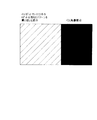
図1は、本発明に係る画像形成装置の第1の実施形態により形成された、本発明の構成要素たる検知パターン及び出力補正用パターンとしての濃度パッチの概略図である。以下この図に基づいて説明を行うが、従来例と同様の構成,作用をするものは同一の番号を付し説明は略す。すなわち、本発明に係る画像形成装置の構成は、図20及び図21に示される構成と同様であり、以下適宜図20及び図21を援用して説明する。
【0066】
本実施形態においては、図20に示されるETB1として周長800mm、厚さ100μmのPVdFの樹脂フィルムを用いている。また、本発明の構成要素たる検知手段としての光学センサとして図2に示したものを用いている。ここで、この光学センサについて説明する。図2は、本実施形態の画像形成装置に適用される、正反射光を検知するタイプの濃度センサの構造図である。
【0067】
図2に示したように本実施形態の、本発明の構成要素たる検知手段としての光学センサは、LEDなどの発光素子301と、フォトダイオードなどの受光素子302からなる。
【0068】
発光素子301による照射光は、ETB1に対し30°の角度で入射し、検知位置303で反射される。この入射角は30°以外の他の角度であっても良い。受光素子302は反射光の照射光と同じ角度で反射された反射光を検知する位置に設けられている。
【0069】
この光学センサで濃度パッチを検知したときに検出される反射光の特性について詳述する。
【0070】
下地となるETB上に照射された光は、図3に示すようにETBの材質固有の屈折率と表面状態で決まる屈折率に応じて反射され、受光素子で検知される。ここに濃度パッチが形成されるとトナーがある部分の下地が隠され、反射光量が減少する(図4)。
【0071】
したがって、図5に示すように濃度パッチのトナー量増加と共に反射光量は減少し、この減少量を基に濃度パッチの濃度を求める。実際には、ETBの使用度合いによって下地の表面状態が変動することで反射光量も変動してしまうので、濃度パッチの反射光量を下地の反射光量で規格化した後、濃度情報に変換するのが一般的である。
【0072】
ところが、有彩色のトナーを検知した場合には問題が生じる。有彩色のトナーに光が照射された場合、色として感じる光が反射される。この反射光は、乱反射光もしくは拡散反射光と呼ばれる。この乱反射光には、色材(=トナー)量の増加に応じて反射光量も増加する、全方向にまんべんなく拡散される、といった特性がある。
【0073】
したがって、本実施形態で用いる光学センサで有彩色の濃度パッチを検知した場合に検知される光は、トナー量の増加と共に減少する下地で反射された光と、トナー量の増加と共に増加するトナーにより反射された光の和になり(図6)、トナー量と反射光量の関係は図19に示したような負性特性をもち、濃度検知に必要なリニアリティを得ることができなかった。
【0074】
そこで、濃度パッチを検知したときの反射光量中の乱反射成分を取り除き、正反射成分のみを取り出す必要がある。
【0075】
ここで、乱反射成分の特性について考えてみる。乱反射成分がトナー量の増加と共に増加することは前述した。
【0076】
そこで、画像形成条件を固定して、露光量(より正確には、ある面積に対する露光部の露光比率)を変えて濃度パッチを形成し、露光量と乱反射成分の光量の関係を調べてみた。
【0077】
このとき、説明のために乱反射成分の測定には図2に示した光学センサと検知位置から受光素子までの距離が等しく、かつ、受光角が照射角と異なるように設定し、乱反射成分のみを検知するようにした光学センサを用いた(図7)。図7は、本発明に係る画像形成装置の第1の実施形態に適用される、乱反射光の特性を検討するためのセンサの構造図である。
【0078】
またこのとき、濃度パッチは図8に示したような4×4ドットマトリクスの繰り返しで形成され、マトリクス中のドットを埋める数を変えることで露光比率を変えている。図8は、本発明に係る画像形成装置の第1の実施形態に適用される4×4ドットマトリクスの一例の概略図である。
【0079】
図8中の数字は、ドットを埋めていく順番を示している。図9に露光量と乱反射光量の関係を示す。図9で横軸の数値は、4×4ドットマトリクス中の埋めたドットの数を示している。図9は、本発明に係る画像形成装置の第1の実施形態における、露光量と乱反射光の関係のグラフである。
【0080】
図9からわかるように、ドットマトリクスの露光比率と乱反射光量の関係はほぼ比例関係になっていることがわかる。つまり、ある露光比率で形成した濃度パッチの乱反射成分のみの反射光量がわかれば、他の露光比率で形成したパッチの乱反射成分の反射光量が予測できるということである。
【0081】
次に、図2に示した本実施形態で使用する光学センサで、有彩色トナーを検知した場合を考えてみる。
【0082】
この場合、検知される光量は正反射成分と乱反射成分の和になることはすでに述べた。ここで、いわゆるべた画像で形成した濃度パッチを検知した場合を考えてみる。
【0083】
このとき、下地上に十分トナーが敷き詰められ下地が見えない状態になっていると考えられ、検知される反射光量中に下地による反射である正反射成分が含まれない状態であると考えることができる。したがって、このとき検知される反射光量は乱反射成分のみとなる。
【0084】
したがって実際には、図7のようなタイプの乱反射光のみを測定するセンサを用いずとも、十分にトナーが敷き詰められた状態においては、図2のタイプのセンサにより乱反射光のみを測定することができる。
【0085】
以上のことより、濃度検知に用いるハーフトーンで形成した濃度パッチと、出力補正に用いるべた画像で形成した濃度パッチを共に図2のセンサにて検知し、べた濃度パッチの出力と、べたとハーフトーンの露光量の比からハーフトーン濃度パッチの出力中の乱反射光量を予測し、ハーフトーン濃度パッチの出力から差し引くことで、正反射光量のみを取り出すことができることがわかる。その結果、濃度パッチの濃度と反射光量の関係は、図19の細実線のような関係になる。
【0086】
このようにして、正反射光量のみを取り出して濃度検知を行うことで、有彩色トナー検知時でも、濃度パッチのトナー量と光学センサの出力の関係にリニアリティが得られ、精度よく濃度検知を行うことができた。
【0087】
次に、本実施形態におけるDmax制御の動作について説明する。図1に本実施形態で用いている、本発明の構成要素たる検知パターンとしての濃度パッチの構成を示す。図1に示すように濃度パッチは4×4ドットマトリクス中の6ドットを塗りつぶしたパターン(図8)の繰り返して形成した部分(本発明の構成要素たる検知パターンとしての濃度検知に用いる部分)とべた画像で形成した部分(本発明の構成要素たる出力補正用パターンとしての出力補正に用いる部分)とから成る。
【0088】
プロセスステーションを制御して、この濃度パッチをETB1上に形成する。この濃度パッチが、光学センサの位置に到達すると、光学センサとしての濃度検知センサ13の出力が取り込まれ、この信号はA/D変換された後CPU15に取り込まれる。このとき、ハーフトーン濃度パッチ,べた濃度パッチともに8回測定を行い、その平均値をそれぞれの濃度パッチの出力としている。
【0089】
このとき、ハーフトーン濃度パッチ部分の出力をVh、べた濃度パッチ部分の出力をVfとした場合、ハーフトーン濃度パッチの正反射成分のみの出力Viは、
Vi=(Vh−V0)−(Vf−V0)×α
と計算される。
【0090】
ここでαは、露光比率100%のときを1、0%のときを0とする補正係数であり、露光比率とそのときのトナー像からの乱反射成分の検知出力が略直線比例関係で近似できる場合には、α=6/16とすればよい。また、V0は発光素子を消灯した場合の光学センサの出力(すなわち、濃度検知センサ13が出力補正用パターン又は検知パターンの検知を行っていない場合の出力値)である。本実施形態においては、反射光量が大きくなるほど光学センサの電圧出力が小さくなる特性の検出回路を用いている。このViが濃度換算表により濃度情報Diに変換される。
【0091】
本実施形態では以上の動作を画像形成条件(本実施形態では現像バイアス)を変えながら5回繰り返し、濃度情報D1〜D5を得る。このとき、D1〜D5の順で濃度が高くなるよう現像バイアスを変えていく。これらの濃度情報から、ハーフトーン濃度パッチの濃度が最適値(ここではDtと呼ぶ)となる現像バイアスを計算する。
【0092】
すべてのパッチを検知すると、図10のように現像バイアスと濃度パッチの濃度の関係が得られる。この中から、濃度の最適値Dtを挟む2点の濃度パッチを取り出し、その2点で直線補間を行うことにより、濃度パッチの濃度が最適値Dtとなる現像バイアスを算出する。図10は、本発明に係る画像形成装置の第1の実施形態における、最適現像バイアスの算出方法の概念図である。
【0093】
以上の操作をすべての色について行い、それぞれの色について画像濃度が最適となる現像バイアスを算出する。
【0094】
以上示したように、本実施形態では、濃度検知用のハーフトーン濃度パッチの出力を、べた濃度パッチの検知出力を用いて補正し、濃度制御を行うことで、正反射光を検知するタイプの濃度センサで有彩色トナーの濃度を検知した場合にも、精度よく濃度制御を行うことができた。
【0095】
(第2の実施形態)
次に本発明に係る画像形成装置の第2の実施形態について説明する。本実施形態の構造も前述の第1の実施形態と同様、図20及び図21を用いて説明した従来技術の構造と同様である。
【0096】
本実施形態では、Dhalf制御について説明する。Dhalf制御とは、電子写真特有の非線形な入出力特性(γ特性)によって、入力画像信号に対して出力濃度がずれて不自然な画像が形成されないよう、γ特性を打ち消して入出力特性をリニアに保つような画像処理を行うことである。
【0097】
この非線形性は、高精細な画像を得るために、3×3ドットマトリクスなどのより細かいマトリクスを単位として中間調を構成した場合により顕著になる。具体的にDhalf制御では、入力画像信号が異なる複数の濃度パッチを光学センサで検知して、入力画像信号と濃度の関係を得、その関係からホストコンピュータからの入力画像信号に対して所望の濃度が出るよう、画像形成装置に入力する画像信号を画像形成装置のコントローラによって変換する(以下γ補正と称す)。
【0098】
このDhalf制御においても、有彩色トナーの検知を行う場合には前述の第1の実施形態と同様の補正を行う必要がある。そこで、本実施形態においても前述の第1の実施形態と同様、検知したい中間調で形成した部分と、補正に用いるべた画像で形成した濃度パッチを用いている(図11)。図11は、本発明に係る画像形成装置の第2の実施形態における、Dhalf制御において用いる本発明の構成要素たる検知パターン及び出力補正用パターンとしての濃度パッチの概略図である。
【0099】
しかしながら、特に3×3ドットマトリクスなどのより細かいマトリクスを単位として中間調を構成した場合は、露光量と乱反射非量の関係も図12に示したように非線形になってしまう。図12は、本発明に係る画像形成装置の第2の実施形態における、乱反射光量と露光量との関係のグラフである。
【0100】
したがって、この場合、前述の第1の実施形態と同様に中間調とべた画像の露光量の比のみから出力補正値を求めると、正確な補正ができなくなってしまう。
【0101】
したがって、本実施形態では中間調とべた画像の露光量の比と乱反射光量の関係をあらかじめ予測しておき、出力の補正に利用している。具体的には、ハーフトーン濃度パッチ部分の出力をVh、べた濃度パッチ部分の出力をVf、発光素子を消灯した場合の光学センサの出力(すなわち、濃度検知センサ13が出力補正用パターン又は検知パターンの検知を行っていない場合の出力値)をV0、とした場合、出力補正後の中間調パッチの出力Vjを、
Vj=(Vh−V0)−(Vf−V0)×β
としている。
【0102】
ここで、βはあらかじめ予測した中間調とべた画像の露光量の比と乱反射光量の関係から求まる値であり、その関係は図13のようになっている。なおこの関係が直線近似その他で近似可能であれば、βは図13のテーブルの代わりに数式を用いて計算してもよい。図13は、本発明に係る画像形成装置の第2の実施形態における、βとハーフトーン及びべたの露光量の比との関係を示すテーブルである。
【0103】
このようにして得られたVjは濃度換算表により濃度情報Djに変換された後、コントローラへ送られ、コントローラはこれらの濃度情報を元にしてγ補正を行う。
【0104】
本実施形態では、このような構成をとることで、前述の第1の実施形態と同様の効果を得ることができると共に、露光量と画像濃度の関係が非線形となりやすい中間調の濃度検知を精度よく行うことができた。
【0105】
(第3の実施形態)
次に、本発明に係る画像形成装置の第3の実施形態について説明する。本実施形態においても、Dhalf制御について説明する。前述の第2の実施形態では第1の実施形態と同様、ハーフトーン画像とべた画像を組み合わせた濃度パッチを用いたDhalf制御について説明した。
【0106】
しかしながら、Dhalf制御ではDmax制御に比べ多数の濃度パッチを形成、検知するため、ハーフトーン画像とべた画像を組み合わせた濃度パッチを用いた場合、濃度パッチの長さの総計が長くなるため、Dhalf制御に要する時間の増加につながっていた。そこで、本実施形態の目的はDhalf制御に要する時間の短縮にある。
【0107】
本実施形態においては、Dhalf制御に用いる濃度パッチとして、図14のような検知したいハーフトーンのみの濃度パッチを所定の数形成する。図14は、本発明に係る画像形成装置の第3の実施形態のDhalf制御に用いる、本発明の構成要素たる検知パターン及び出力補正用パターンとしての濃度パッチの概略図である。
【0108】
前述の第1の実施形態、第2の実施形態で説明したようにハーフトーンの濃度を検知するには、べた画像で形成した濃度パッチも検知し補正を行う必要がある。
【0109】
本実施形態では、補正に用いるべた部分の出力を、Dhalf制御に先立って行われるDmax制御時に検知したべた画像で形成した濃度パッチの出力が求める。以下にこの方法を説明する。
【0110】
前述の第1の実施形態で説明したように、補正後のセンサ出力の目標値を挟む2点の濃度パッチを取り出し、直線補間を行うことで最適な現像バイアスを決定している。
【0111】
このとき、最適現像バイアスを挟む2点の現像バイアスで形成した濃度パッチのべた部分の出力についても直線補間を行い、最適現像バイアス時のべた部分の出力を推測する(図15)。図15は、本発明に係る画像形成装置の第3の実施形態における、最適現像バイアス時のべた画像濃度を算出する方法を示す概念図である。
【0112】
この値を記憶しておき、Dhalf制御実行時に、前述の第2の実施形態と同様の計算を行うことで検知した濃度パッチの濃度情報を得る。コントローラは、これらの濃度情報を基にしてγ補正を行う。
【0113】
以上説明したように、本実施形態では、前述の第1の実施形態及び第2の実施形態と同様の効果を得ることができると共に、Dmax制御時に検知したべた画像で形成した濃度パッチの出力から最適現像バイアス時のべたパッチの出力を求め、この値を記憶しハーフトーン濃度パッチの濃度検知に用いることで、Dhalf制御時の濃度パッチを小さくすることができ、Dhalf制御に要する時間の短縮とトナー消費量の低減を図ることができる。
【0114】
【発明の効果】
以上説明したように本発明によれば、濃度検知用のパターンとは別に出力補正用のパターンを形成、検知し、出力補正用パターンの出力に基づいて濃度検知パターンの出力を補正することで、濃度検知用パターンの濃度と出力の関係にリニアリティが得られ、精度よく濃度制御を行うことができる。
【0115】
また、この出力補正値を少なくとも出力補正用パターンの出力と、前記検知パターンと出力補正用パターンの露光量の比に基づいて求めることで、より精度よく濃度検知を行うことができる。
【図面の簡単な説明】
【図1】本発明に係る画像形成装置の第1の実施形態により形成された濃度パッチの概略図である。
【図2】本発明に係る画像形成装置の第1の実施形態に適用される、正反射光を検知するタイプの濃度センサの構造図である。
【図3】本発明及び従来の画像形成装置において適用される、照射光と正反射光の関係を示す概念図である。
【図4】本発明及び従来の画像形成装置において適用される、ETB上にトナーが存在する場合の照射光と正反射光の関係を示す概念図である。
【図5】本発明及び従来の画像形成装置において適用される、トナー量と正反射光量の関係を示すグラフである。
【図6】本発明及び従来の画像形成装置において適用される、有彩色トナーを検知した場合の照射光と反射光の概念図である。
【図7】本発明に係る画像形成装置の第1の実施形態に適用される、乱反射光の特性を検討するためのセンサの構造図である。
【図8】本発明に係る画像形成装置の第1の実施形態に適用される4×4ドットマトリクスの一例の概略図である。
【図9】本発明に係る画像形成装置の第1の実施形態における、露光量と乱反射光の関係のグラフである。
【図10】本発明に係る画像形成装置の第1の実施形態における、最適現像バイアスの算出方法の概念図である。
【図11】本発明に係る画像形成装置の第2の実施形態における、Dhalf制御において用いる濃度パッチの概略図である。
【図12】本発明に係る画像形成装置の第2の実施形態における、乱反射光量と露光量との関係のグラフである。
【図13】本発明に係る画像形成装置の第2の実施形態における、βとハーフトーン及びべたの露光量の比との関係を示すテーブルである。
【図14】本発明に係る画像形成装置の第3の実施形態のDhalf制御に用いる濃度パッチの概略図である。
【図15】本発明に係る画像形成装置の第3の実施形態における、最適現像バイアス時のべた画像濃度を算出する方法を示す概念図である。
【図16】本発明及び従来の画像形成装置において適用される、乱反射光量とトナー量との関係のグラフである。
【図17】本発明及び従来の画像形成装置において適用される、トナーに光を照射した際の照射光と乱反射光との関係の概念図である。
【図18】本発明及び従来の画像形成装置において適用される、乱反射光を検知するタイプの濃度センサの一例の構造図である。
【図19】本発明及び従来の画像形成装置において適用される、有彩色トナーを正反射光検知型の濃度センサで検知した場合のトナー量と反射光量の関係のグラフである。
【図20】従来の画像形成装置の一部構成図である。
【図21】図20に示される画像形成装置が具備するプロセスステーションの構成図である。
【符号の説明】
1 ETB(静電吸着搬送ベルト)
3 転写ローラ
4 バイアス電源
5 吸着ローラ
6 吸着対向ローラ
7 駆動ローラ
8,9 テンションローラ
13 濃度検知センサ
14 クリーニングブレード
15 CPU
17 バイアス電源
201,202,203,204 プロセスステーション
211 感光体
212 帯電器
213 露光光学系
214 走査光
215 現像ローラ
216 トナー容器
217 クリーニングブレード
218 廃トナー容器
301 発光素子
302 受光素子
303 検知位置[0001]
BACKGROUND OF THE INVENTION
The present invention relates to an image forming apparatus and an image forming method using an electrophotographic process.
[0002]
[Prior art]
Conventionally, as an image forming apparatus, various methods such as an electrophotographic method, a thermal transfer method, and an ink jet method are used. Among these, those using the electrophotographic method are superior to other methods in terms of high speed, high image quality, and quietness, and have been popularized in recent years.
[0003]
This electrophotography is also divided into various methods.For example, in addition to the well-known multiple transfer method and intermediate transfer member method, a color image is superimposed on the surface of the photosensitive member, and then transferred to a batch to form an image. There are a multiple development system to be performed, an inline system in which a plurality of different color image forming means (process stations) are arranged in series, and a developed image is transferred onto a transfer material conveyed by a transfer belt.
[0004]
Of these methods, the in-line method is excellent because it is possible to increase the speed and the number of times of image transfer is small, which is advantageous for image quality.
[0005]
FIG. 20 is a partial configuration diagram of a conventional image forming apparatus and shows an inline configuration. In FIG. 20, an electrostatic attraction / conveying belt (hereinafter referred to as ETB) 1 is stretched by each of a driving roller 7, a suction counter roller 6,
[0006]
Process stations 201 (yellow), 202 (magenta), 203 (cyan), and 204 (black) as process devices as constituent elements of the present invention are arranged in a row on the peripheral surface of the
[0007]
Further, the
[0008]
Conventionally, the ETB1 has a thickness of 50 to 200 μm and a volume resistivity of 109-1016For example, a resin film such as PVdF, ETFE, polyimide, PET, polycarbonate or the like of about Ωcm, or a fluororesin such as PTFE on urethane rubber on a rubber base layer such as EPDM having a thickness of about 0.5 to 2 mm. A dispersion provided as a surface layer is used.
[0009]
Here, the image forming process will be described. First, the image forming process in the process station will be described with reference to FIG. FIG. 21 is a configuration diagram of a process station included in the image forming apparatus shown in FIG. The description is made using a yellow process station, but the same applies to other color stations.
[0010]
In the configuration of the process station shown in FIG. 21, a
[0011]
This latent image is developed by the developing
[0012]
Next, the transfer process will be described. In a generally used reversal development method, when the photosensitive member is, for example, a negative-polarity OPC photosensitive member, a negative-polarity toner is used when developing the exposed portion. Therefore, a positive transfer bias is applied to the transfer roller 3 from the bias power source 4. Here, a low resistance roller is generally used as the transfer roller.
[0013]
In the actual printing process, considering the moving speed of the
[0014]
When the above process is completed, the ETB 1 is neutralized by the
[0015]
Also, the image density varies depending on the temperature and humidity conditions in which the image forming apparatus is used and the degree of use of the process station. In order to correct this variation, the image density is controlled. Here, this image density control will be described.
[0016]
Conventionally, with regard to image density control, a density patch image of each color is formed on a photoconductor, an intermediate transfer body (hereinafter referred to as ITB), or an ETB, and this is a density detection sensor as a detection means as a component of the present invention. 13 is used to adjust the maximum density and halftone gradation characteristics of each color by feeding back to process formation conditions such as high pressure conditions and laser power.
[0017]
In general, the
[0018]
The purpose of image density control is to keep the maximum density of each color constant (hereinafter referred to as Dmax control) and to maintain the halftone gradation characteristics linearly with respect to the image signal (hereinafter referred to as Dhal control). .
[0019]
In addition, Dmax control has a large meaning of keeping the color balance of each color constant, and preventing scattering of overlaid characters and fixing failure due to excessive toner loading.
[0020]
Specifically, in the Dmax control, a plurality of density patches formed by changing the image forming conditions are detected by an optical sensor, and a condition for obtaining a desired maximum density is calculated from the result, and the image forming conditions are changed. Here, it is often preferable that the density patch is formed in a halftone.
[0021]
The reason is that when a so-called solid image is detected, the width of the change in the sensor output with respect to the change in the toner amount becomes small, and sufficient detection accuracy cannot be obtained.
[0022]
On the other hand, Dhalf control cancels the γ characteristic in order to prevent the output density from deviating from the input image signal due to the nonlinear input / output characteristic (γ characteristic) peculiar to electrophotography. Image processing is performed to keep the input / output characteristics linear.
[0023]
Specifically, a plurality of density patches having different input image signals are detected by an optical sensor to obtain a relationship between the input image signal and the density, and a desired density is obtained with respect to the input image signal from the host computer based on the relationship. As described above, the image signal input to the image forming apparatus is converted by the controller of the image forming apparatus. This Dhalf control is generally performed after the image forming conditions are determined by Dmax control.
[0024]
The density patch formed on the ETB is electrostatically collected in the process apparatus by a cleaning process. At the time of the cleaning process, a bias opposite in polarity to the charging polarity of the toner is applied to the photosensitive member, the toner is attracted to the photosensitive member at the transfer portion, and is scraped off by the
[0025]
[Problems to be solved by the invention]
However, in the case of the prior art as described above, the following problems have occurred. As described above, the density detection sensor generally irradiates the density patch with the light source and detects the reflected light intensity with the light receiving sensor, but the system is roughly divided into the following two systems.
[0026]
・ Method to detect diffuse reflection component of reflected light
・ Method to detect the specular component of reflected light
[0027]
First, a method for detecting the irregular reflection component will be described in detail. The irregular reflection component is a reflection component that is perceived as a color, and the amount of reflected light has a characteristic that it increases as the amount of color material of the density patch, that is, the amount of toner increases (FIG. 16). FIG. 16 is a graph showing the relationship between the amount of irregularly reflected light and the amount of toner applied in the present invention and the conventional image forming apparatus.
[0028]
Another characteristic is that the reflected light diffuses evenly from the density patch in all directions (FIG. 17). FIG. 17 is a conceptual diagram of a relationship between irradiation light and irregular reflection light when the toner is irradiated with light, which is applied in the present invention and the conventional image forming apparatus.
[0029]
The type of density sensor that detects the irregular reflection component is configured such that the irradiation angle α and the light reception angle β are different as shown in FIG. FIG. 18 is a structural diagram of an example of a density sensor for detecting diffusely reflected light, which is applied in the present invention and the conventional image forming apparatus.
[0030]
However, when the density sensor for detecting the irregular reflection detects the density of the black toner, the black toner absorbs light, so that the reflected light from the black toner cannot be detected.
[0031]
Therefore, in this case, for example, a method of detecting the density of the black toner by using a chromatic color for the background portion of the density patch and measuring the amount of reflected light of the background hidden by the black toner has been devised. .
[0032]
By the way, when using an in-line image forming system having a plurality of photoconductors as described in the prior art, the density patches are formed and detected on the photoconductor in order to reduce the number of density sensors. Instead, it is conceivable to form density patches on the ETB or ITB and detect the densities of all colors with a single density sensor.
[0033]
However, it is necessary to adjust the resistance value of the transfer belt and the intermediate transfer member in order to ensure the paper conveyance force and the image stability on the intermediate transfer member. The body is often black or dark gray.
[0034]
Therefore, when detecting the density of the black toner on the ETB (ITB), light is not reflected from the density patch or the background, and the black toner cannot be detected by a density sensor that detects irregular reflection. Therefore, it is necessary to use a type of density sensor that detects regular reflection light described later.
[0035]
Next, a method for detecting the regular reflection component of the reflected light will be described in detail. As shown in FIG. 3, a sensor that detects specularly reflected light detects light reflected in a direction that is symmetric with respect to the irradiation angle α with respect to the normal line of the base surface (ETB surface). FIG. 3 is a conceptual diagram showing the relationship between irradiation light and regular reflection light applied in the present invention and the conventional image forming apparatus.
[0036]
The amount of reflected light depends on the refractive index specific to the material of the base (ETB) and the reflectance determined by the surface state, and feels glossy. This light is maximized when no toner is present on the substrate.
[0037]
When the density patch is formed on the ground, the ground is hidden and the reflected light disappears in a portion where the toner is present as shown in FIG. Therefore, as shown in FIG. 5, the relationship between the toner amount of the density patch and the reflected light amount decreases as the toner amount increases. FIG. 4 is a conceptual diagram showing the relationship between irradiation light and regular reflection light when toner is present on the ETB, which is applied in the present invention and the conventional image forming apparatus, and FIG. 6 is a graph showing the relationship between the amount of toner and the amount of specular reflection applied in the image forming apparatus.
[0038]
Density sensors that detect specularly reflected light mainly detect reflected light from the ground, not reflected light from the toner, so that density detection can be performed regardless of the color of the toner and the ground, so diffusely reflected light This is more advantageous than a concentration sensor of the type that detects
[0039]
In general, the reflected light amount of the regular reflection component is larger than the reflected light amount of the irregular reflection component, and the density sensor of the type that detects regular reflected light is more advantageous in terms of the detection accuracy of the density sensor. Even when density detection is performed, it is desirable to use a type of density sensor that detects specularly reflected light.
[0040]
By the way, in a density sensor that detects specularly reflected light, the amount of reflected light also varies when the surface state of the ground varies depending on the degree of use. Therefore, it is effective to normalize the reflected light amount of the density patch with the reflected light amount of the ground and then perform correction such as conversion to density information.
[0041]
However, a problem occurs when chromatic toner is detected by a density sensor that detects regular reflection light. As described above, when light is applied to the density patch of the chromatic color toner, irregular reflection light increases as the toner amount increases, and the reflection light is diffused in all directions.
[0042]
Therefore, the light detected by the density sensor is the sum of the regular reflection component and the irregular reflection component as shown in FIG. FIG. 6 is a conceptual diagram of irradiation light and reflected light when chromatic toner is detected, which is applied in the present invention and the conventional image forming apparatus.
[0043]
As shown in FIG. 19, the relationship between the toner amount and the reflected light amount at this time is the sum of a fine solid line that is a regular reflection characteristic and a broken line that is an irregular reflection characteristic, and exhibits a negative characteristic like a thick solid line. For this reason, the linearity necessary for density detection cannot be obtained, and the density detection accuracy is not sufficient. FIG. 19 is a graph showing the relationship between the amount of toner and the amount of reflected light when chromatic color toner is detected by a regular reflection light detection type density sensor, which is applied in the present invention and the conventional image forming apparatus.
[0044]
In order to solve this problem, as disclosed in JP-A-5-249787, a density sensor or light receiving element for detecting irregular reflection and a density sensor or light receiving element for detecting regular reflection are provided, and the chromatic color toner is irregularly reflected. A component and black toner are detected by a regular reflection component, or a polarizing plate is provided in front of a light emitting element and a light receiving element as disclosed in JP-A-6-250480, and the polarization states of the irregular reflection component and the regular reflection component are changed. A method has been devised to extract only the specular reflection component using the difference. However, either method has led to an increase in the cost of the density sensor.
[0045]
SUMMARY OF THE INVENTION Accordingly, an object of the present invention is to provide an image forming apparatus capable of accurately detecting toner density even with a regular reflection detection type density sensor having a simple configuration.PlaceIt is to provide.
[0046]
[Means for Solving the Problems]
In order to achieve the above object, an image forming apparatus according to the present invention includes an image carrier on which a latent image is formed by exposure, charging means for charging the image carrier to a predetermined polarity, and the image A developing device that visualizes the latent image formed on the carrier with chromatic toner; a detection pattern forming unit that controls the process device to form a predetermined detection pattern; and In an image forming apparatus comprising a detecting means for detecting and a means for controlling an image forming condition based on an output of the detecting means, the detecting means calculates a reflection intensity of light when the detection pattern is irradiated with light. Measuring means, and means for detecting light reflected in a direction symmetric with respect to the normal of the surface on which the detection pattern is formed with respect to the irradiation direction of the light. The process unit is controlled to form a solid pattern in which a predetermined area is entirely exposed, and the detection means detects the solid pattern, and based on the detection result of the solid pattern, the value of the detection result of the detection pattern When correcting Vh, the value Vh of the detection result of the detection patternTheThe detection result value of the solid pattern is Vf, the value relating to the exposure ratio of the detection pattern to the solid pattern is α, and the detection means when the detection means is not detecting the solid pattern or the detection pattern. When the output value is V0, Vi = (Vh−V0) − (Vf−V0) × αAnd correct.
[0062]
DETAILED DESCRIPTION OF THE INVENTION
Exemplary embodiments of the present invention will be described in detail below with reference to the drawings. However, the dimensions, materials, shapes, relative arrangements, and the like of the components described in this embodiment are not intended to limit the scope of the present invention only to those unless otherwise specified. Absent.
[0063]
In the following drawings, the same reference numerals are given to the members described in the drawings used in the description of the prior art and the members similar to the members described in the drawings described above..
[0064]
(First embodiment)
Hereinafter, a first embodiment of an image forming apparatus according to the present invention will be described with reference to the accompanying drawings. However, the embodiment of the present invention is not limited thereto. Further, only the characteristic part of the invention will be mainly described.
[0065]
FIG. 1 is a schematic diagram of density patches as detection patterns and output correction patterns, which are constituent elements of the present invention, formed by the first embodiment of the image forming apparatus according to the present invention. In the following, description will be made based on this figure, but those having the same configuration and function as those of the conventional example will be given the same reference numerals and description thereof will be omitted. That is, the configuration of the image forming apparatus according to the present invention is the same as the configuration shown in FIGS. 20 and 21, and will be described below with appropriate reference to FIGS.
[0066]
In the present embodiment, a PVdF resin film having a circumference of 800 mm and a thickness of 100 μm is used as the
[0067]
As shown in FIG. 2, the optical sensor as the detection means of the present embodiment of the present embodiment includes a
[0068]
Irradiation light from the
[0069]
The characteristics of the reflected light detected when the optical sensor detects a density patch will be described in detail.
[0070]
As shown in FIG. 3, the light irradiated on the base ETB is reflected according to the refractive index specific to the material of the ETB and the refractive index determined by the surface state, and is detected by the light receiving element. When a density patch is formed here, the base of the portion where the toner is present is hidden, and the amount of reflected light is reduced (FIG. 4).
[0071]
Therefore, as shown in FIG. 5, the amount of reflected light decreases as the toner amount of the density patch increases, and the density of the density patch is obtained based on this decreased amount. Actually, the amount of reflected light also fluctuates when the surface state of the ground fluctuates depending on the degree of use of the ETB. Therefore, the reflected light amount of the density patch is normalized with the reflected light quantity of the ground, and then converted to density information. It is common.
[0072]
However, a problem occurs when chromatic toner is detected. When the chromatic toner is irradiated with light, the light that is felt as a color is reflected. This reflected light is called irregular reflection light or diffuse reflection light. This irregularly reflected light has such characteristics that the amount of reflected light increases as the amount of color material (= toner) increases, and that the diffused light is evenly diffused in all directions.
[0073]
Therefore, the light detected when the chromatic density patch is detected by the optical sensor used in the present embodiment is reflected by the light reflected by the ground that decreases as the toner amount increases and the toner that increases as the toner amount increases. The sum of the reflected light was obtained (FIG. 6), and the relationship between the toner amount and the amount of reflected light had negative characteristics as shown in FIG. 19, and the linearity necessary for density detection could not be obtained.
[0074]
Therefore, it is necessary to remove the irregular reflection component from the reflected light amount when the density patch is detected, and to extract only the regular reflection component.
[0075]
Here, let us consider the characteristics of the irregular reflection component. As described above, the irregular reflection component increases as the toner amount increases.
[0076]
Therefore, while fixing the image forming conditions, changing the exposure amount (more precisely, the exposure ratio of the exposed portion with respect to a certain area) to form a density patch, the relationship between the exposure amount and the light quantity of the irregular reflection component was examined.
[0077]
At this time, for the purpose of explanation, the irregular reflection component is measured by setting the optical sensor shown in FIG. 2 and the distance from the detection position to the light receiving element to be equal and the light receiving angle is different from the irradiation angle. An optical sensor adapted to detect was used (FIG. 7). FIG. 7 is a structural diagram of a sensor for examining characteristics of irregularly reflected light, which is applied to the first embodiment of the image forming apparatus according to the present invention.
[0078]
At this time, the density patch is formed by repeating a 4 × 4 dot matrix as shown in FIG. 8, and the exposure ratio is changed by changing the number of dots to be filled in the matrix. FIG. 8 is a schematic diagram of an example of a 4 × 4 dot matrix applied to the first embodiment of the image forming apparatus according to the present invention.
[0079]
The numbers in FIG. 8 indicate the order in which dots are filled. FIG. 9 shows the relationship between the exposure amount and the amount of irregularly reflected light. In FIG. 9, the numbers on the horizontal axis indicate the number of dots embedded in the 4 × 4 dot matrix. FIG. 9 is a graph showing the relationship between the exposure amount and the irregularly reflected light in the first embodiment of the image forming apparatus according to the present invention.
[0080]
As can be seen from FIG. 9, the relationship between the exposure ratio of the dot matrix and the amount of irregularly reflected light is substantially proportional. That is, if the reflected light amount of only the irregular reflection component of the density patch formed at a certain exposure ratio is known, the reflected light amount of the irregular reflection component of the patch formed at another exposure ratio can be predicted.
[0081]
Next, let us consider a case where chromatic toner is detected by the optical sensor used in this embodiment shown in FIG.
[0082]
In this case, as described above, the detected light amount is the sum of the regular reflection component and the irregular reflection component. Consider a case where a density patch formed with a so-called solid image is detected.
[0083]
At this time, it is considered that the toner is sufficiently spread on the background and the background cannot be seen, and it is considered that the detected reflected light amount does not include the regular reflection component that is reflection by the background. it can. Therefore, the amount of reflected light detected at this time is only the irregular reflection component.
[0084]
Therefore, actually, only the irregularly reflected light can be measured by the sensor of the type shown in FIG. 2 in a state where the toner is sufficiently spread without using a sensor that measures only the irregularly reflected light of the type as shown in FIG. it can.
[0085]
From the above, the density patch formed with the halftone used for density detection and the density patch formed with the solid image used for output correction are both detected by the sensor of FIG. It can be seen that only the regular reflection light quantity can be extracted by predicting the irregular reflection light quantity in the output of the halftone density patch from the ratio of the exposure amount of the tone and subtracting it from the output of the halftone density patch. As a result, the relationship between the density of the density patch and the amount of reflected light is as shown by a thin solid line in FIG.
[0086]
In this way, density detection is performed by extracting only the amount of specularly reflected light, and even when detecting chromatic toner, linearity is obtained in the relationship between the toner amount of the density patch and the output of the optical sensor, and density detection is performed with high accuracy. I was able to.
[0087]
Next, the operation of Dmax control in this embodiment will be described. FIG. 1 shows a configuration of a density patch as a detection pattern, which is a component of the present invention, used in the present embodiment. As shown in FIG. 1, the density patch is a part formed by repeating a pattern (FIG. 8) in which 6 dots in a 4 × 4 dot matrix are filled (a part used for density detection as a detection pattern as a component of the present invention). A portion formed by a solid image (a portion used for output correction as an output correction pattern, which is a component of the present invention).
[0088]
The process station is controlled to form this density patch on ETB1. When the density patch reaches the position of the optical sensor, the output of the
[0089]
At this time, when the output of the halftone density patch portion is Vh and the output of the solid density patch portion is Vf, the output Vi of only the regular reflection component of the halftone density patch is
Vi = (Vh−V0) − (Vf−V0) × α
Is calculated.
[0090]
Here, α is a correction coefficient that assumes 1 when the exposure ratio is 100% and 0 when the exposure ratio is 0%. The exposure ratio and the detection output of the irregular reflection component from the toner image at that time can be approximated by a substantially linear proportional relationship. In this case, α = 6/16 may be set. V0 is the output of the optical sensor when the light emitting element is turned off (that is, the output value when the
[0091]
In the present embodiment, the above operation is repeated five times while changing the image forming conditions (development bias in the present embodiment) to obtain density information D1 to D5. At this time, the developing bias is changed so that the density increases in the order of D1 to D5. From these density information, the development bias at which the density of the halftone density patch becomes the optimum value (referred to herein as Dt) is calculated.
[0092]
When all the patches are detected, the relationship between the developing bias and the density of the density patch is obtained as shown in FIG. From these, two density patches sandwiching the optimum density value Dt are taken out, and linear interpolation is performed at the two points to calculate a developing bias at which the density patch density becomes the optimum value Dt. FIG. 10 is a conceptual diagram of an optimum developing bias calculation method in the first embodiment of the image forming apparatus according to the present invention.
[0093]
The above operation is performed for all the colors, and the development bias that optimizes the image density for each color is calculated.
[0094]
As described above, in the present embodiment, the output of the halftone density patch for density detection is corrected using the detection output of the solid density patch, and the density control is performed to detect the specular reflection light. Even when the density sensor detects the density of the chromatic color toner, the density control can be performed with high accuracy.
[0095]
(Second Embodiment)
Next, a second embodiment of the image forming apparatus according to the present invention will be described. The structure of this embodiment is the same as the structure of the prior art described with reference to FIGS. 20 and 21 as in the first embodiment.
[0096]
In this embodiment, Dhalf control will be described. Dhalf control is a non-linear input / output characteristic (γ characteristic) unique to electrophotography, which cancels the γ characteristic and makes the input / output characteristic linear so that an output image is shifted from the input image signal and an unnatural image is not formed. It is to perform image processing that keeps the image.
[0097]
This non-linearity becomes more prominent when a halftone is configured with a finer matrix such as a 3 × 3 dot matrix as a unit in order to obtain a high-definition image. Specifically, in Dhalf control, a plurality of density patches having different input image signals are detected by an optical sensor to obtain a relationship between the input image signal and the density, and based on the relationship, a desired density is obtained with respect to the input image signal from the host computer. The image signal input to the image forming apparatus is converted by the controller of the image forming apparatus (hereinafter referred to as γ correction) so that the
[0098]
Also in this Dhalf control, when detecting chromatic color toner, it is necessary to perform the same correction as in the first embodiment. Therefore, in this embodiment as well, as in the first embodiment described above, a portion formed in a halftone to be detected and a density patch formed from a solid image used for correction are used (FIG. 11). FIG. 11 is a schematic diagram of a density patch as a detection pattern and an output correction pattern, which are constituent elements of the present invention, used in Dhalf control in the second embodiment of the image forming apparatus according to the present invention.
[0099]
However, particularly when a halftone is configured with a finer matrix such as a 3 × 3 dot matrix as a unit, the relationship between the exposure amount and the irregular reflection non-amount also becomes nonlinear as shown in FIG. FIG. 12 is a graph showing the relationship between the amount of irregularly reflected light and the exposure amount in the second embodiment of the image forming apparatus according to the present invention.
[0100]
Therefore, in this case, if the output correction value is obtained only from the ratio of the exposure amount of the solid image and the solid image as in the first embodiment, accurate correction cannot be performed.
[0101]
Therefore, in the present embodiment, the relationship between the ratio between the halftone and the exposure amount of the solid image and the amount of irregularly reflected light is predicted in advance and used for output correction. Specifically, the output of the halftone density patch part is Vh, the output of the solid density patch part is Vf, and the output of the optical sensor when the light emitting element is turned off (that is, the
Vj = (Vh−V0) − (Vf−V0) × β
It is said.
[0102]
Here, β is a value obtained from the relationship between the halftone predicted in advance and the ratio of the exposure amount of the solid image and the amount of diffusely reflected light, and the relationship is as shown in FIG. If this relationship can be approximated by linear approximation or the like, β may be calculated using an equation instead of the table of FIG. FIG. 13 is a table showing the relationship between β and the ratio of the halftone and the solid exposure amount in the second embodiment of the image forming apparatus according to the present invention.
[0103]
Vj obtained in this way is converted into density information Dj by the density conversion table and then sent to the controller. The controller performs γ correction based on these density information.
[0104]
In this embodiment, by adopting such a configuration, it is possible to obtain the same effect as that of the first embodiment described above, and to perform halftone density detection in which the relationship between the exposure amount and the image density is likely to be nonlinear. Well done.
[0105]
(Third embodiment)
Next, a third embodiment of the image forming apparatus according to the present invention will be described. Also in the present embodiment, Dhalf control will be described. In the second embodiment described above, Dhalf control using a density patch that combines a halftone image and a solid image has been described, as in the first embodiment.
[0106]
However, in the Dhalf control, a larger number of density patches are formed and detected than in the Dmax control. When a density patch combining a halftone image and a solid image is used, the total length of the density patches becomes longer. Led to an increase in the time required for Therefore, an object of the present embodiment is to shorten the time required for Dhalf control.
[0107]
In this embodiment, a predetermined number of halftone-only density patches as shown in FIG. 14 are formed as density patches used for Dhalf control. FIG. 14 is a schematic diagram of density patches as detection patterns and output correction patterns, which are constituent elements of the present invention, used for Dhalf control of the third embodiment of the image forming apparatus according to the present invention.
[0108]
As described in the first and second embodiments described above, in order to detect the halftone density, it is necessary to detect and correct density patches formed from solid images.
[0109]
In this embodiment, the output of the solid patch used for the correction is obtained as the output of the density patch formed by the solid image detected during the Dmax control performed prior to the Dhalf control. This method will be described below.
[0110]
As described in the first embodiment, the optimum developing bias is determined by taking out two density patches that sandwich the target value of the sensor output after correction and performing linear interpolation.
[0111]
At this time, linear interpolation is also performed for the output of the solid portion of the density patch formed by the two development biases sandwiching the optimal development bias, and the output of the solid portion at the optimal development bias is estimated (FIG. 15). FIG. 15 is a conceptual diagram showing a method for calculating the solid image density at the optimum developing bias in the third embodiment of the image forming apparatus according to the present invention.
[0112]
This value is stored, and density information of the detected density patch is obtained by performing the same calculation as in the second embodiment described above when executing the Dhalf control. The controller performs γ correction based on the density information.
[0113]
As described above, in this embodiment, the same effects as those of the first and second embodiments described above can be obtained, and the density patch formed from the solid image detected during the Dmax control can be obtained. By obtaining the output of the solid patch at the optimum development bias, storing this value and using it for density detection of the halftone density patch, the density patch at the time of Dhalf control can be reduced, and the time required for Dhalf control can be shortened. The toner consumption can be reduced.
[0114]
【The invention's effect】
As described above, according to the present invention, an output correction pattern is formed and detected separately from the density detection pattern, and the output of the density detection pattern is corrected based on the output of the output correction pattern. Linearity is obtained in the relationship between the density and output of the density detection pattern, and density control can be performed with high accuracy.
[0115]
Further, by obtaining the output correction value based on at least the output of the output correction pattern and the ratio of the exposure amount of the detection pattern and the output correction pattern, the density detection can be performed with higher accuracy.
[Brief description of the drawings]
FIG. 1 is a schematic diagram of a density patch formed by a first embodiment of an image forming apparatus according to the present invention.
FIG. 2 is a structural diagram of a density sensor of a type that detects regular reflection light, which is applied to the first embodiment of the image forming apparatus according to the present invention.
FIG. 3 is a conceptual diagram showing a relationship between irradiation light and regular reflection light applied in the present invention and a conventional image forming apparatus.
FIG. 4 is a conceptual diagram illustrating a relationship between irradiation light and regular reflection light when toner is present on an ETB, which is applied in the present invention and a conventional image forming apparatus.
FIG. 5 is a graph showing a relationship between a toner amount and a regular reflection light amount applied in the present invention and a conventional image forming apparatus.
FIG. 6 is a conceptual diagram of irradiation light and reflected light when chromatic toner is detected, which is applied in the present invention and a conventional image forming apparatus.
FIG. 7 is a structural diagram of a sensor for examining characteristics of irregularly reflected light applied to the first embodiment of the image forming apparatus according to the present invention.
FIG. 8 is a schematic view of an example of a 4 × 4 dot matrix applied to the first embodiment of the image forming apparatus according to the present invention.
FIG. 9 is a graph showing a relationship between an exposure amount and irregularly reflected light in the first embodiment of the image forming apparatus according to the present invention.
FIG. 10 is a conceptual diagram of a method for calculating an optimum developing bias in the first embodiment of the image forming apparatus according to the present invention.
FIG. 11 is a schematic diagram of density patches used in Dhalf control in the second embodiment of the image forming apparatus according to the present invention.
FIG. 12 is a graph showing the relationship between the amount of irregularly reflected light and the exposure amount in the second embodiment of the image forming apparatus according to the present invention.
FIG. 13 is a table showing a relationship between β and a ratio of halftone and solid exposure amounts in the second embodiment of the image forming apparatus according to the present invention.
FIG. 14 is a schematic diagram of density patches used for Dhalf control of the third embodiment of the image forming apparatus according to the present invention.
FIG. 15 is a conceptual diagram illustrating a method for calculating a solid image density at an optimum developing bias in the third embodiment of the image forming apparatus according to the present invention.
FIG. 16 is a graph showing the relationship between the amount of irregularly reflected light and the amount of toner applied in the present invention and a conventional image forming apparatus.
FIG. 17 is a conceptual diagram of a relationship between irradiation light and irregular reflection light when the toner is irradiated with light, which is applied in the present invention and the conventional image forming apparatus.
FIG. 18 is a structural diagram of an example of a density sensor that detects irregularly reflected light, which is applied in the present invention and a conventional image forming apparatus.
FIG. 19 is a graph showing the relationship between the amount of toner and the amount of reflected light when chromatic color toner is detected by a regular reflection light detection type density sensor, which is applied in the present invention and a conventional image forming apparatus.
FIG. 20 is a partial configuration diagram of a conventional image forming apparatus.
21 is a configuration diagram of a process station included in the image forming apparatus shown in FIG.
[Explanation of symbols]
1 ETB (electrostatic adsorption conveyor belt)
3 Transfer roller
4 Bias power supply
5 Suction roller
6 Adsorption counter roller
7 Drive roller
8,9 Tension roller
13 Concentration detection sensor
14 Cleaning blade
15 CPU
17 Bias power supply
201, 202, 203, 204 Process station
211 photoconductor
212 Charger
213 Exposure optical system
214 Scanning light
215 Developing roller
216 Toner container
217 Cleaning blade
218 Waste toner container
301 Light Emitting Element
302 Light receiving element
303 Detection position
Claims (6)
該像担持体を所定の極性に帯電する帯電手段と、
該像担持体上に形成された潜像を有彩色トナーで可視化する現像装置と、
を含むプロセス装置と、
該プロセス装置を制御して所定の検知パターンを形成する検知パターン形成手段と、
該検知パターンを検知する検知手段と、
該検知手段の出力に基づいて、画像形成条件を制御する手段と
を備える画像形成装置において、
前記検知手段が、前記検知パターンに光を照射した際の光の反射強度を測定する手段であり、かつ、前記光の照射方向に対し前記検知パターンが形成された面の法線について対称な方向に反射される光を検知する手段であり、
前記検知パターン形成手段が、前記プロセス装置を制御して所定の面積内を全面露光したべたパターンを形成すると共に、前記検知手段が該べたパターンを検知し、該べたパターンの検知結果に基づいて、前記検知パターンの検知結果の値Vhの補正を行う際、
該検知パターンの検知結果の値Vhを、前記べたパターンの検知結果の値をVf、前記べたパターンに対する前記検知パターンの露光比率に関する値をα、前記検知手段が前記べたパターン又は前記検知パターンの検知を行っていない場合の前記検知手段の出力値をV0とした場合、Vi=(Vh−V0)−(Vf−V0)×αなるViと補正することを特徴とする画像形成装置。An image carrier on which a latent image is formed by exposure; and
Charging means for charging the image carrier to a predetermined polarity;
A developing device for visualizing the latent image formed on the image carrier with chromatic toner;
A process device comprising:
Detection pattern forming means for controlling the process device to form a predetermined detection pattern;
Detection means for detecting the detection pattern;
An image forming apparatus comprising: means for controlling image forming conditions based on the output of the detecting means;
The detection means is a means for measuring the reflection intensity of light when the detection pattern is irradiated with light, and a direction symmetric with respect to the normal of the surface on which the detection pattern is formed with respect to the light irradiation direction Means for detecting the light reflected by
The detection pattern forming means controls the process apparatus to form a solid pattern that has been exposed in a predetermined area, and the detection means detects the solid pattern, based on the detection result of the solid pattern, When correcting the detection result value Vh of the detection pattern,
The detection result value Vh of the detection pattern is Vf, the detection result value of the solid pattern is Vf, the value relating to the exposure ratio of the detection pattern to the solid pattern is α, and the detection means detects the solid pattern or the detection pattern. When the output value of the detecting means when V is not performed is V0, Vi is corrected to Vi = (Vh−V0) − (Vf−V0) × α.
Priority Applications (2)
| Application Number | Priority Date | Filing Date | Title |
|---|---|---|---|
| JP2000141350A JP4612762B2 (en) | 2000-05-15 | 2000-05-15 | Image forming apparatus |
| US09/852,748 US6512898B2 (en) | 2000-05-15 | 2001-05-11 | Image forming apparatus for detecting the density of toner |
Applications Claiming Priority (1)
| Application Number | Priority Date | Filing Date | Title |
|---|---|---|---|
| JP2000141350A JP4612762B2 (en) | 2000-05-15 | 2000-05-15 | Image forming apparatus |
Publications (3)
| Publication Number | Publication Date |
|---|---|
| JP2001324840A JP2001324840A (en) | 2001-11-22 |
| JP2001324840A5 JP2001324840A5 (en) | 2009-11-26 |
| JP4612762B2 true JP4612762B2 (en) | 2011-01-12 |
Family
ID=18648479
Family Applications (1)
| Application Number | Title | Priority Date | Filing Date |
|---|---|---|---|
| JP2000141350A Expired - Fee Related JP4612762B2 (en) | 2000-05-15 | 2000-05-15 | Image forming apparatus |
Country Status (2)
| Country | Link |
|---|---|
| US (1) | US6512898B2 (en) |
| JP (1) | JP4612762B2 (en) |
Families Citing this family (14)
| Publication number | Priority date | Publication date | Assignee | Title |
|---|---|---|---|---|
| JP4745512B2 (en) * | 2001-02-09 | 2011-08-10 | キヤノン株式会社 | Color image forming apparatus |
| US6775489B2 (en) * | 2001-06-07 | 2004-08-10 | Canon Kabushiki Kaisha | Image forming apparatus capable of detecting density of toner image |
| JP2003162111A (en) * | 2001-11-27 | 2003-06-06 | Canon Inc | Color image forming apparatus |
| JP4136706B2 (en) * | 2003-02-20 | 2008-08-20 | キヤノン株式会社 | Color image forming apparatus and density detection pattern generation method thereof |
| EP1457840B1 (en) | 2003-03-14 | 2014-07-30 | Ricoh Company, Ltd. | Colour image forming apparatus, which controls the image density by evaluating a reflection signal and a diffuse reflection signal of an optical detecting unit |
| US20060093382A1 (en) * | 2004-11-03 | 2006-05-04 | Ertel John P | System and method for accurately tracking printable material |
| JP4594115B2 (en) * | 2005-01-20 | 2010-12-08 | 京セラミタ株式会社 | Image forming apparatus |
| CN1892487B (en) | 2005-06-30 | 2010-12-29 | 株式会社理光 | Attachment conversion method for image forming apparatus |
| KR100795160B1 (en) * | 2007-03-22 | 2008-01-16 | 주식회사 아트닉스 | Apparatus for face detection and recognition and method for face detection and recognition |
| JP5268020B2 (en) | 2008-10-22 | 2013-08-21 | 株式会社リコー | Image forming apparatus |
| JP2013003211A (en) | 2011-06-13 | 2013-01-07 | Ricoh Co Ltd | Method for converting diffused reflected light output, method for converting powder adhesion amount, and image forming apparatus |
| JP2013113989A (en) * | 2011-11-28 | 2013-06-10 | Brother Ind Ltd | Image forming apparatus and method for correcting image formation |
| US9042755B2 (en) * | 2013-10-04 | 2015-05-26 | Xerox Corporation | Printer control using optical and electrostatic sensors |
| US20170016091A1 (en) * | 2014-05-27 | 2017-01-19 | Questek Innovations Llc | Highly processable single crystal nickel alloys |
Citations (3)
| Publication number | Priority date | Publication date | Assignee | Title |
|---|---|---|---|---|
| JPH0392874A (en) * | 1989-09-05 | 1991-04-18 | Minolta Camera Co Ltd | Image forming device |
| JPH0511552A (en) * | 1991-07-05 | 1993-01-22 | Minolta Camera Co Ltd | Digital image forming device |
| JPH09292765A (en) * | 1996-02-29 | 1997-11-11 | Ricoh Co Ltd | Device for measuring quantity of sticking toner for electrophotography |
Family Cites Families (8)
| Publication number | Priority date | Publication date | Assignee | Title |
|---|---|---|---|---|
| JP2918045B2 (en) * | 1988-10-28 | 1999-07-12 | 株式会社リコー | Image density control device |
| JPH05249787A (en) | 1992-03-03 | 1993-09-28 | Canon Inc | Image forming device |
| JP2729976B2 (en) | 1993-02-25 | 1998-03-18 | スタンレー電気株式会社 | Measuring device for toner adhesion of transfer type color printer |
| US5625857A (en) * | 1994-01-18 | 1997-04-29 | Hitachi, Ltd. | Image forming apparatus which measures deposit amounts of toner |
| US5630195A (en) * | 1995-05-12 | 1997-05-13 | Ricoh Company, Ltd. | Color toner density sensor and image forming apparatus using the same |
| US5933680A (en) * | 1996-02-29 | 1999-08-03 | Canon Kabushiki Kaisha | Image processing apparatus and method for optimizing an image formation condition |
| JP3667971B2 (en) * | 1998-02-04 | 2005-07-06 | 株式会社リコー | Image forming apparatus |
| JP3532472B2 (en) * | 1999-04-27 | 2004-05-31 | シャープ株式会社 | Image forming device |
-
2000
- 2000-05-15 JP JP2000141350A patent/JP4612762B2/en not_active Expired - Fee Related
-
2001
- 2001-05-11 US US09/852,748 patent/US6512898B2/en not_active Expired - Lifetime
Patent Citations (3)
| Publication number | Priority date | Publication date | Assignee | Title |
|---|---|---|---|---|
| JPH0392874A (en) * | 1989-09-05 | 1991-04-18 | Minolta Camera Co Ltd | Image forming device |
| JPH0511552A (en) * | 1991-07-05 | 1993-01-22 | Minolta Camera Co Ltd | Digital image forming device |
| JPH09292765A (en) * | 1996-02-29 | 1997-11-11 | Ricoh Co Ltd | Device for measuring quantity of sticking toner for electrophotography |
Also Published As
| Publication number | Publication date |
|---|---|
| JP2001324840A (en) | 2001-11-22 |
| US20020006288A1 (en) | 2002-01-17 |
| US6512898B2 (en) | 2003-01-28 |
Similar Documents
| Publication | Publication Date | Title |
|---|---|---|
| JP4016949B2 (en) | Image forming apparatus and image forming method | |
| US7551866B2 (en) | Image forming method and apparatus with improved conversion capability of amount of toner adhesion | |
| JP4612762B2 (en) | Image forming apparatus | |
| US6775489B2 (en) | Image forming apparatus capable of detecting density of toner image | |
| US8369729B2 (en) | Image forming apparatus with varying transfer bias | |
| JP5197825B2 (en) | Image forming apparatus | |
| JP4794226B2 (en) | Image forming apparatus | |
| JP2006284892A (en) | Image forming apparatus | |
| JP2006251652A (en) | Image forming apparatus | |
| JP4963382B2 (en) | Image forming apparatus | |
| JP4603908B2 (en) | Image forming apparatus | |
| JP2009168906A (en) | Image forming apparatus | |
| JP6244828B2 (en) | Image forming apparatus | |
| JP4834252B2 (en) | Image forming apparatus | |
| JP2005300918A (en) | Image forming apparatus | |
| JP2007086817A (en) | Image formation apparatus and image formation method | |
| JP4136706B2 (en) | Color image forming apparatus and density detection pattern generation method thereof | |
| JP2003215883A (en) | Image forming device | |
| JP2005326539A (en) | Image forming apparatus | |
| US7899348B2 (en) | Image forming apparatus with developing bias correcting portion that changes a developing density adjustment pattern | |
| JP2009276686A (en) | Image forming apparatus | |
| US10996591B2 (en) | Image forming apparatus | |
| JP3441595B2 (en) | Electrophotographic toner adhesion amount measuring device | |
| JP3454450B2 (en) | Image forming device | |
| JP3051470B2 (en) | Image forming apparatus and image forming method |
Legal Events
| Date | Code | Title | Description |
|---|---|---|---|
| A621 | Written request for application examination |
Free format text: JAPANESE INTERMEDIATE CODE: A621 Effective date: 20070515 |
|
| A977 | Report on retrieval |
Free format text: JAPANESE INTERMEDIATE CODE: A971007 Effective date: 20090907 |
|
| A521 | Written amendment |
Free format text: JAPANESE INTERMEDIATE CODE: A523 Effective date: 20091007 |
|
| A131 | Notification of reasons for refusal |
Free format text: JAPANESE INTERMEDIATE CODE: A131 Effective date: 20091027 |
|
| A521 | Written amendment |
Free format text: JAPANESE INTERMEDIATE CODE: A523 Effective date: 20091224 |
|
| A131 | Notification of reasons for refusal |
Free format text: JAPANESE INTERMEDIATE CODE: A131 Effective date: 20100518 |
|
| A521 | Written amendment |
Free format text: JAPANESE INTERMEDIATE CODE: A523 Effective date: 20100716 |
|
| TRDD | Decision of grant or rejection written | ||
| A01 | Written decision to grant a patent or to grant a registration (utility model) |
Free format text: JAPANESE INTERMEDIATE CODE: A01 Effective date: 20101012 |
|
| A01 | Written decision to grant a patent or to grant a registration (utility model) |
Free format text: JAPANESE INTERMEDIATE CODE: A01 |
|
| A61 | First payment of annual fees (during grant procedure) |
Free format text: JAPANESE INTERMEDIATE CODE: A61 Effective date: 20101016 |
|
| FPAY | Renewal fee payment (event date is renewal date of database) |
Free format text: PAYMENT UNTIL: 20131022 Year of fee payment: 3 |
|
| R150 | Certificate of patent or registration of utility model |
Free format text: JAPANESE INTERMEDIATE CODE: R150 |
|
| LAPS | Cancellation because of no payment of annual fees |