JP4611663B2 - Overlay error measuring method, overlay error measuring apparatus, and semiconductor device manufacturing method - Google Patents
Overlay error measuring method, overlay error measuring apparatus, and semiconductor device manufacturing method Download PDFInfo
- Publication number
- JP4611663B2 JP4611663B2 JP2004138913A JP2004138913A JP4611663B2 JP 4611663 B2 JP4611663 B2 JP 4611663B2 JP 2004138913 A JP2004138913 A JP 2004138913A JP 2004138913 A JP2004138913 A JP 2004138913A JP 4611663 B2 JP4611663 B2 JP 4611663B2
- Authority
- JP
- Japan
- Prior art keywords
- image signal
- center position
- evaluation function
- pattern
- symmetry evaluation
- Prior art date
- Legal status (The legal status is an assumption and is not a legal conclusion. Google has not performed a legal analysis and makes no representation as to the accuracy of the status listed.)
- Expired - Fee Related
Links
Images


Description
本発明は、半導体デバイスの製造工程で半導体ウェーハ上に形成されたパターンの重ね合わせ誤差を測定する重ね合わせ誤差測定方法、重ね合わせ誤差測定装置、及びそれらを用いた半導体デバイスの製造方法に関する。 The present invention relates to an overlay error measurement method for measuring an overlay error of a pattern formed on a semiconductor wafer in a semiconductor device manufacturing process, an overlay error measuring apparatus, and a semiconductor device manufacturing method using them.
IC,LSI等の半導体デバイスの製造工程では、いわゆるフォトリソグラフィー技術により、回路パターンを形成している。フォトリソグラフィー技術では、縮小投影露光装置を用いて、レチクルやフォトマスクに形成されたパターンを、感光材料(レジスト)を塗布した半導体ウェーハ上に転写する。そして、現像処理によってレジストパターンを形成し、さらに、このレジストパターンをマスクとしてドライエッチングにより回路パターンを形成する。半導体デバイスを半導体ウェーハ上に構成するためには、このような回路パターンの形成を20回〜30回程度繰り返す必要がある。 In a manufacturing process of a semiconductor device such as an IC or LSI, a circuit pattern is formed by a so-called photolithography technique. In the photolithography technique, a pattern formed on a reticle or photomask is transferred onto a semiconductor wafer coated with a photosensitive material (resist) using a reduction projection exposure apparatus. Then, a resist pattern is formed by development processing, and a circuit pattern is formed by dry etching using this resist pattern as a mask. In order to configure a semiconductor device on a semiconductor wafer, it is necessary to repeat such circuit pattern formation about 20 to 30 times.
半導体デバイスの回路パターンの重ね合わせ精度は、SIA(Semiconductor Industry Association) Roadmap 2000年の表1「Product Critical Level Lithography Requirements」に示されているような精度が要求される。 The superimposition accuracy of the circuit pattern of the semiconductor device is required to be as shown in Table 1 “Product Critical Level Lithography Requirements” of SIA (Semiconductor Insulator Association) Roadmap 2000.
一般に、回路パターンの重ね合わせ精度の検査は、半導体デバイスの製造工程で回路パターンの他に測定用パターンを形成し、重ね合わせ誤差測定装置を用いてこの測定用パターンの重ね合わせ誤差を測定することにより行われている。重ね合わせ誤差測定装置は、測定用パターンの像の画像信号を検出し、検出した画像信号を処理して測定用パターンの中心位置を検出し、測定用パターンの中心位置のずれ量を求めるものである。 In general, inspection of circuit pattern overlay accuracy involves forming a measurement pattern in addition to the circuit pattern in the semiconductor device manufacturing process, and measuring the overlay error of this measurement pattern using an overlay error measuring device. It is done by. The overlay error measuring device detects an image signal of an image of a measurement pattern, processes the detected image signal to detect a center position of the measurement pattern, and obtains a deviation amount of the center position of the measurement pattern. is there.
パターンの像の画像信号からパターンの中心位置を検出する手法として、特許文献1に記載の対称性マッチング法が知られている。対称性マッチング法では、画像信号の波形の仮想中心位置から左右等しい距離にある画像信号の差の二乗を積算する対称性評価関数を用い、仮想中心位置を変化させながら対称性評価関数の値を算出して、対称性評価関数の値が極小となる仮想中心位置をパターンの中心位置として検出する。
一般に、対称性マッチング法では、対称性評価関数の積算範囲を広くする程、データ量が多くなり安定した検出を行うことができる。しかしながら、測定対象のパターンの段差に非対称性が有ると、画像信号の波形が非対称となるため、対称性評価関数の形状に歪みが生じ、測定誤差が発生するという問題があった。 In general, in the symmetry matching method, as the integration range of the symmetry evaluation function is increased, the amount of data increases and stable detection can be performed. However, if there is an asymmetry in the level difference of the pattern to be measured, the waveform of the image signal becomes asymmetric, which causes a problem in that the shape of the symmetry evaluation function is distorted and a measurement error occurs.
これに対し、特許文献1には、画像信号の波形が非対称的になっている領域を求め、この領域を除いた対称性の良い領域を局所的な区間として積算範囲とする技術が開示されている。しかしながら、画像信号の波形が非対称的になっている領域を求めるためには、画像信号の極大点、極小点、変曲点等の特徴点を検出して比較する複雑な処理が必要となる。 On the other hand, Patent Document 1 discloses a technique in which an area in which the waveform of an image signal is asymmetric is obtained and an area with good symmetry excluding this area is used as a local section as an integration range. Yes. However, in order to obtain a region in which the waveform of the image signal is asymmetrical, a complicated process for detecting and comparing feature points such as maximum points, minimum points, and inflection points of the image signal is required.
本発明の課題は、対称性マッチング法を用い、簡単な処理でパターンの段差の非対称性の影響を除去して、パターンの重ね合わせ誤差を精度良く測定することである。また、本発明の課題は、パターンの重ね合わせ精度を向上して、高品質な半導体デバイスを製造することである。 An object of the present invention is to measure the pattern overlay error with high accuracy by using the symmetry matching method and removing the influence of the pattern step asymmetry by a simple process. Another object of the present invention is to improve the pattern overlay accuracy and manufacture a high-quality semiconductor device.
本発明の第1の特徴は、対称性マッチング法において、対称性評価関数の極小値が最も小さくなるように、対称性評価関数の積算範囲を設定することである。 The first feature of the present invention is that in the symmetry matching method, the integration range of the symmetry evaluation function is set so that the minimum value of the symmetry evaluation function is minimized.
また、本発明の第2の特徴は、対称性マッチング法において、対称性評価関数の極小値が最も小さくなるように、受光系のフォーカス位置を調整することである。このとき、受光系のフォーカス位置が合焦点位置に近い程、受光系で受光する光の強度が強くなり、パターンの像の画像信号が大きくなるので、受光系のフォーカス位置に応じて対称性評価関数の極小値を正規化する。 The second feature of the present invention is that in the symmetry matching method, the focus position of the light receiving system is adjusted so that the minimum value of the symmetry evaluation function is minimized. At this time, the closer the focus position of the light receiving system is to the in-focus position, the stronger the intensity of light received by the light receiving system and the larger the image signal of the pattern image, so symmetry evaluation is performed according to the focus position of the light receiving system. Normalize the local minimum of the function.
従来、対称性マッチング法では、対称性評価関数の値が極小となる位置が重要であって、極小値の大きさ自体は重要視されていなかった。本発明では、対称性評価関数の極小値の大きさに着目した。パターンの段差がほぼ対称であると、画像信号の波形がほぼ対称となるため、対称性評価関数の極小値は零に近くなる。一方、パターンの段差に非対称性が有ると、画像信号の波形が非対称となるため、対称性評価関数の極小値は大きくなる。本発明では、対称性評価関数の極小値が最も小さくなるように、対称性評価関数の積算範囲を設定し、または受光系のフォーカス位置を調整する。これにより、パターンの段差の非対称性の影響が最も除去されて、検出される中心位置が真の値に近づく。画像信号の波形が非対称的になっている領域を求める複雑な処理は、必要ない。 Conventionally, in the symmetry matching method, the position where the value of the symmetry evaluation function is minimized is important, and the magnitude of the minimum value itself is not regarded as important. In the present invention, attention is paid to the minimum value of the symmetry evaluation function. If the pattern steps are substantially symmetric, the waveform of the image signal is substantially symmetric, and the minimum value of the symmetry evaluation function is close to zero. On the other hand, if there is an asymmetry in the pattern steps, the waveform of the image signal becomes asymmetric, and the minimum value of the symmetry evaluation function increases. In the present invention, the integration range of the symmetry evaluation function is set or the focus position of the light receiving system is adjusted so that the minimum value of the symmetry evaluation function is minimized. Thereby, the influence of the asymmetry of the pattern step is most removed, and the detected center position approaches the true value. There is no need for complicated processing for obtaining a region where the waveform of the image signal is asymmetric.
本発明の半導体デバイスの製造方法は、上記のいずれかの特徴を備えた重ね合わせ誤差測定方法又は重ね合わせ誤差測定装置を用いて、パターンの重ね合わせ精度を検査するものである。 The semiconductor device manufacturing method of the present invention is to inspect the overlay accuracy of a pattern using the overlay error measuring method or overlay error measuring apparatus having any one of the above features.
本発明によれば、対称性評価関数の極小値が最も小さくなるように、対称性評価関数の積算範囲を設定することにより、簡単な処理でパターンの段差の非対称性の影響を除去して、パターンの重ね合わせ誤差を精度良く測定することができる。 According to the present invention, by setting the integration range of the symmetry evaluation function so that the minimum value of the symmetry evaluation function becomes the smallest, the influence of the asymmetry of the pattern step is removed by simple processing, Pattern overlay errors can be accurately measured.
また、本発明によれば、受光系のフォーカス位置に応じて対称性評価関数の極小値を正規化し、正規化した極小値が最も小さくなるように、受光系のフォーカス位置を調整することにより、簡単な処理でパターンの段差の非対称性の影響を除去して、パターンの重ね合わせ誤差を精度良く測定することができる。 Further, according to the present invention, the local minimum value of the symmetry evaluation function is normalized according to the focus position of the light receiving system, and the focus position of the light receiving system is adjusted so that the normalized minimum value is minimized. It is possible to accurately measure the overlay error of the pattern by removing the influence of the asymmetry of the pattern step by a simple process.
本発明の半導体デバイスの製造方法によれば、パターンの重ね合わせ精度を向上して、高品質な半導体デバイスを製造することができる。 According to the semiconductor device manufacturing method of the present invention, it is possible to improve the pattern overlay accuracy and manufacture a high-quality semiconductor device.
図1は、本発明の一実施の形態による重ね合わせ誤差測定装置の概略構成を示す図である。重ね合わせ誤差測定装置は、チャック10、ステージ11、光源20、投光系、受光系、検出器32,33、画像信号処理回路40、制御装置50、及びステージ駆動回路60を含んで構成されている。
FIG. 1 is a diagram showing a schematic configuration of an overlay error measuring apparatus according to an embodiment of the present invention. The overlay error measuring device includes a
表面に測定用パターンが形成された半導体ウェーハ1が、チャック10上に固定されている。ステージ11は、チャック10を搭載しながら、XY方向へ移動し、θ方向に回転し、またZ軸方向に移動する。ステージ駆動回路60は、制御装置50の制御により、ステージ11を駆動する。ステージ11のXY方向への移動及びθ方向への回転によって、半導体ウェーハ1上の測定用マークの位置決めが行われる。また、ステージ11のZ軸方向への移動によって、受光系のフォーカス位置が調整される。
A semiconductor wafer 1 having a measurement pattern formed on the surface is fixed on a
なお、ステージ11により半導体ウェーハ1を移動する代わりに、受光系を移動させることによって、測定用マークの位置決め及び受光系のフォーカス位置の調整を行ってもよい。
Instead of moving the semiconductor wafer 1 by the
光源20は、例えば水銀ランプ等から成り、照明光を発生する。投光系は、ライトガイド21、照明用開口絞り22、照明用リレーレンズ23、ハーフミラー24、及び対物レンズ25を含んで構成されている。光源20から発生した照明光は、ライトガイド21、照明用開口絞り22、照明用リレーレンズ23を通り、ハーフミラー24で反射されて、対物レンズ25から半導体ウェーハ1の表面へ照射される。
The
受光系は、対物レンズ25、ハーフミラー24、結像レンズ30、及びハーフミラー31を含んで構成されている。半導体ウェーハ1の表面からの反射光は、対物レンズ25で集光され、ハーフミラー24を透過した後、結像レンズ30を通って、ハーフミラー31へ入射する。
The light receiving system includes an
ハーフミラー31へ入射した反射光の約半分は、ハーフミラー31を透過して検出器32の受光面で結像する。ハーフミラー31へ入射した反射光の残り約半分は、ハーフミラー31で反射されて検出器33の受光面で結像する。検出器32,33は、CCDラインセンサーから成り、一方はX方向、他方はY方向に複数の画素が配列されている。検出器32,33は、受光面で受光した光の強度に応じた画像信号を画像信号処理回路40へ出力する。
About half of the reflected light incident on the
なお、検出器32,33の代わりに2次元のエリアセンサーを用いてもよく、その場合、ハーフミラー31は不要である。
Note that a two-dimensional area sensor may be used instead of the
画像信号処理回路40は、A/D変換器、画像メモリ、ディジタル信号処理装置(DPS)等を含んで構成されている。画像信号処理回路40は、検出器32,33からの画像信号をディジタル信号に変換した後、対称性評価関数の値を算出する処理と、対称性評価関数の値が極小となる仮想中心位置を測定用パターンの中心位置として検出する処理と、測定用パターンの中心位置のずれ量を求める処理とを行う。
The image
まず、画像信号処理回路40のこれらの処理について説明する。図2(a)は測定用パターンの一例の断面図、図2(b)は測定用パターンの像の画像信号の一例を示す図である。一般に、測定用パターンは、エッチングパターンとレジストパターンとで構成されている。図2(a)はこれらのうちレジストパターンの例を示しており、半導体ウェーハの表面に形成された膜2の上に、2つのレジストパターン3a,3bが形成されている。図2(a)の測定用パターンに対し、検出器32は、一例として図2(b)に示す画像信号を出力する。
First, these processes of the image
図2(b)に示す画像信号について、画像信号処理回路40は、まず、仮想中心位置のX座標を変化させながら、対称性評価関数の値を算出する処理を行う。対称性評価関数は、画像信号の波形の仮想中心位置から左右等しい距離にある画像信号の差の二乗を積算するもので、その詳細は特許文献1に記載されている。図3は、算出された対称性評価関数の値の一例を示す図である。本例は、図2(b)に示す画像信号について、積算範囲をW1に設定して対称性評価関数の値を算出した例を示している。
For the image signal shown in FIG. 2B, the image
続いて、画像信号処理回路40は、対称性評価関数の値が極小となる仮想中心位置をレジストパターン3a,3bの中心位置として検出する処理を行う。図3に示した例では、対称性評価関数の値が極小となる仮想中心位置のX座標X1を検出し、これを2つのレジストパターン3a,3bのX方向の中心位置とする。
Subsequently, the image
画像信号処理回路40は、エッチングパターンについても、同様にしてX方向の中心位置の検出を行う。そして、エッチングパターンの中心位置とレジストパターンの中心位置とのずれ量を求める処理を行って、X方向の重ね合わせ誤差を測定する。画像信号処理回路40は、検出器33が出力するY方向の画像信号についても同様の処理を行い、Y方向の重ね合わせ誤差を測定する。
The image
次に、本発明の第1の特徴について説明する。本発明の第1の特徴は、画像信号処理回路40が、対称性評価関数の値を算出する処理において、対称性評価関数の極小値が最も小さくなるように、対称性評価関数の積算範囲を設定することである。
Next, the first feature of the present invention will be described. The first feature of the present invention is that the integration range of the symmetry evaluation function is set so that the image
ここで、対称性評価関数の極小値が最も小さくなる積算範囲は、例えば、複数の異なる積算範囲で対称性評価関数の値を算出し、その結果に基づいて決定する。以下、図2(b)に示す画像信号について、積算範囲をW1及びW2として対称性評価関数の値を算出した例について説明する。 Here, the integration range in which the minimum value of the symmetry evaluation function becomes the smallest is determined based on the result of calculating the value of the symmetry evaluation function in a plurality of different integration ranges, for example. Hereinafter, with respect to the image signal shown in FIG. 2B, an example in which the value of the symmetry evaluation function is calculated with the integration ranges W1 and W2 will be described.
図4は、対称性評価関数の値が極小となる部分を拡大して示した図であって、図4(a)は積算範囲をW1とした例、図4(b)は積算範囲をW2とした例である。図4(a)に示すように、積算範囲をW1とした例では、対称性評価関数の値が極小となる仮想中心位置のX座標はX1となり、極小値はほぼ零となった。一方、図4(b)に示すように、積算範囲をW2とした例では、対称性評価関数の値が極小となる仮想中心位置のX座標はX2となり、極小値が大きくなった。 FIG. 4 is an enlarged view of a portion where the value of the symmetry evaluation function is minimized. FIG. 4A shows an example in which the integration range is W1, and FIG. 4B shows the integration range W2. It is an example. As shown in FIG. 4A, in the example in which the integration range is W1, the X coordinate of the virtual center position where the value of the symmetry evaluation function is minimum is X1, and the minimum value is almost zero. On the other hand, as shown in FIG. 4B, in the example in which the integration range is W2, the X coordinate of the virtual center position where the value of the symmetry evaluation function is minimum is X2, and the minimum value is large.
これらの結果から、対称性評価関数の積算範囲をW1に設定すると、積算範囲をW2に設定する場合に比べ、対称性評価関数の極小値が小さくなるので、パターンの段差の非対称性の影響が少なくなる。従って、2つのレジストパターン3a,3bのX方向の中心位置として検出されるX座標X1は、X2よりも、真の値に近いものとなる。
From these results, when the integration range of the symmetry evaluation function is set to W1, the minimum value of the symmetry evaluation function is smaller than in the case where the integration range is set to W2. Less. Therefore, the X coordinate X1 detected as the center position in the X direction of the two resist
なお、以上説明した例では積算範囲をW1及びW2の2つとしていたが、本発明では、適当な範囲及び数の複数の積算範囲で対称性評価関数の値を算出し、その結果に基づいて積算範囲を決定すればよい。対称性評価関数の極小値が最も小さくなるように、対称性評価関数の積算範囲を設定することにより、パターンの段差の非対称性の影響が最も除去されて、検出される中心位置が真の値に近づく。 In the example described above, there are two integration ranges W1 and W2. However, in the present invention, the value of the symmetry evaluation function is calculated in an appropriate range and a plurality of integration ranges, and based on the result. What is necessary is just to determine the integration range. By setting the integration range of the symmetry evaluation function so that the minimum value of the symmetry evaluation function becomes the smallest, the influence of the asymmetry of the pattern step is most eliminated, and the detected center position is a true value. Get closer to.
次に、本発明の第2の特徴について説明する。本発明の第2の特徴は、対称性評価関数の極小値が最も小さくなるように、受光系のフォーカス位置を調整することである。このとき、受光系のフォーカス位置が合焦点位置に近い程、受光系で受光した光の強度が強くなり、パターンの像の画像信号が大きくなるので、受光系のフォーカス位置に応じて対称性評価関数の極小値を正規化する。 Next, the second feature of the present invention will be described. The second feature of the present invention is that the focus position of the light receiving system is adjusted so that the minimum value of the symmetry evaluation function is minimized. At this time, the closer the focus position of the light receiving system is to the in-focus position, the stronger the intensity of light received by the light receiving system and the larger the image signal of the pattern image. Therefore, symmetry evaluation according to the focus position of the light receiving system Normalize the local minimum of the function.
ここで、対称性評価関数の極小値が最も小さくなるフォーカス位置は、例えば、複数の異なるフォーカス位置で測定用パターンの像の画像信号を検出し、各フォーカス位置で検出した画像信号について対称性評価関数の値を算出して決定する。図1に示した実施の形態おいて、ステージ駆動回路60は、制御回路50の制御により、ステージ11をZ軸方向へ駆動し、受光系のフォーカス位置を変化させる。検出器32,33は、複数の異なるフォーカス位置で測定用パターンの像の画像信号を検出する。画像信号処理回路40は、各フォーカス位置で検出した画像信号について対称性評価関数の値を算出する処理を行い、フォーカス位置に応じて対称性評価関数の極小値を正規化する。
Here, the focus position at which the minimum value of the symmetry evaluation function becomes the smallest is, for example, detecting the image signal of the image of the measurement pattern at a plurality of different focus positions, and evaluating the symmetry of the image signal detected at each focus position. Calculate and determine the value of the function. In the embodiment shown in FIG. 1, the
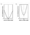
図5は、正規化した対称性評価関数の極小値のフォーカス位置による変化を示す図であって、図5(a)は測定用パターンの段差がほぼ対称の場合の例、図5(b)は測定用パターンの段差が非対称性を有する場合の例である。図5(a)に示すように、測定用パターンの段差がほぼ対称の場合、正規化した対称性評価関数の極小値はフォーカス位置によらずほぼ一定となる。一方、図5(b)に示すように、測定用パターンの段差が非対称性を有する場合、正規化した対称性評価関数の極小値はフォーカス位置によって変化する。 FIG. 5 is a diagram showing a change in the normalized symmetry evaluation function depending on the focus position, and FIG. 5A shows an example in which the steps of the measurement pattern are almost symmetrical, and FIG. Is an example where the steps of the measurement pattern have asymmetry. As shown in FIG. 5A, when the level difference of the measurement pattern is substantially symmetric, the minimum value of the normalized symmetry evaluation function is substantially constant regardless of the focus position. On the other hand, as shown in FIG. 5B, when the step of the measurement pattern has asymmetry, the minimum value of the normalized symmetry evaluation function varies depending on the focus position.
図5(b)に示す例では、フォーカス位置F1で、正規化した対称性評価関数の極小値が最も小さくなっており、パターンの段差の非対称性の影響が最も少なくなっている。従って、制御回路50によりステージ駆動回路60を制御してステージ11をZ軸方向へ駆動し、受光系のフォーカス位置をこの位置に調整することにより、パターンの段差の非対称性の影響が最も除去されて、検出される中心位置が真の値に近づく。
In the example shown in FIG. 5B, the minimum value of the normalized symmetry evaluation function is the smallest at the focus position F1, and the influence of the asymmetry of the pattern step is the smallest. Therefore, by controlling the
なお、正規化した対称性評価関数の極小値が最も小さくなるフォーカス位置は、合焦点位置と一致するとは限らない。本発明では、合焦点位置に関係なく、正規化した対称性評価関数の極小値が最も小さくなるように、受光系のフォーカス位置を決定すればよい。 Note that the focus position where the minimum value of the normalized symmetry evaluation function is the smallest does not always coincide with the in-focus position. In the present invention, the focus position of the light receiving system may be determined so that the minimum value of the normalized symmetry evaluation function is minimized regardless of the in-focus position.
以上説明した実施の形態によれば、画像信号処理回路40が、対称性評価関数の極小値が最も小さくなるように、対称性評価関数の積算範囲を設定することにより、簡単な処理でパターンの段差の非対称性の影響を除去して、パターンの重ね合わせ誤差を精度良く測定することができる。
According to the embodiment described above, the image
また、以上説明した実施の形態によれば、画像信号処理回路40が、受光系のフォーカス位置に応じて対称性評価関数の極小値を正規化し、制御回路50、ステージ駆動回路60及びステージ11からなるフォーカス調整手段が、正規化した極小値が最も小さくなるように、受光系のフォーカス位置を調整することにより、簡単な処理でパターンの段差の非対称性の影響を除去して、パターンの重ね合わせ誤差を精度良く測定することができる。
Further, according to the embodiment described above, the image
本発明の重ね合わせ誤差測定方法又は重ね合わせ誤差測定装置を用いて、パターンの重ね合わせ精度を検査することにより、パターンの重ね合わせ精度を向上して、高品質な半導体デバイスを製造することができる。 By using the overlay error measuring method or overlay error measuring apparatus of the present invention to inspect the pattern overlay accuracy, the pattern overlay accuracy can be improved and a high-quality semiconductor device can be manufactured. .
1 半導体ウェーハ
2 膜
3a,3b レジストパターン
10 チャック
11 ステージ
20 光源
21 ライトガイド
22 照明用開口絞り
23 照明用リレーレンズ
24,31 ハーフミラー
25 対物レンズ
30 結像レンズ
32,33 検出器
40 画像信号処理回路
50 制御装置
60 ステージ駆動回路
DESCRIPTION OF SYMBOLS 1
Claims (6)
対称性評価関数の極小値が最も小さくなるように、前記画像信号の波形の仮想中心位置から左右等しい距離にある画像信号の差の二乗の積算範囲を設定することを特徴とする重ね合わせ誤差測定方法。 Detecting the image signal of the image of the pattern formed on the semiconductor wafer, calculating the value of the symmetry evaluation function that integrates the square of the difference between the image signals at the same distance from the virtual center position of the waveform of the image signal; An overlay error measurement method for detecting a virtual center position where a value of a symmetry evaluation function is a minimum as a pattern center position and obtaining a shift amount of the pattern center position,
An overlay error measurement characterized in that an integration range of squares of differences between image signals at equal distances from the virtual center position of the waveform of the image signal is set so that the minimum value of the symmetry evaluation function is minimized. Method.
前記光源が発生した照明光を半導体ウェーハの表面へ照射する投光系と、
半導体ウェーハの表面からの反射光を受光する受光系と、
前記受光系で受光した光の強度から半導体ウェーハ上に形成されたパターンの像の画像信号を検出する画像信号検出手段と、
前記画像信号検出手段が検出した画像信号の波形の仮想中心位置から左右等しい距離にある画像信号の差の二乗を積算する対称性評価関数の値を算出する処理と、
対称性評価関数の値が極小となる仮想中心位置をパターンの中心位置として検出する処理と、
パターンの中心位置のずれ量を求める処理とを行う画像信号処理手段とを備えた重ね合わせ誤差測定装置であって、
前記画像信号処理手段は、対称性評価関数の極小値が最も小さくなるように、前記画像信号の波形の仮想中心位置から左右等しい距離にある画像信号の差の二乗の積算範囲を設定することを特徴とする重ね合わせ誤差測定装置。 A light source that generates illumination light;
A light projecting system for irradiating the surface of the semiconductor wafer with illumination light generated by the light source;
A light receiving system for receiving reflected light from the surface of the semiconductor wafer;
Image signal detection means for detecting an image signal of an image of a pattern formed on the semiconductor wafer from the intensity of light received by the light receiving system;
A process of calculating a value of a symmetry evaluation function that integrates the square of the difference between image signals at equal distances from the virtual center position of the waveform of the image signal detected by the image signal detection means;
A process of detecting a virtual center position where the value of the symmetry evaluation function is a minimum as a center position of the pattern;
An overlay error measuring device comprising image signal processing means for performing processing for obtaining a shift amount of a center position of a pattern,
The image signal processing means sets an integration range of squares of differences of image signals at equal distances from the virtual center position of the waveform of the image signal so that the minimum value of the symmetry evaluation function is minimized. Characteristic overlay error measuring device.
受光系のフォーカス位置に応じて対称性評価関数の極小値を正規化し、正規化した極小値が最も小さくなるように、受光系フォーカス位置を調整することを特徴とする重ね合わせ誤差測定方法。 Symmetry that adjusts the focus position of the light receiving system to detect the image signal of the image of the pattern formed on the semiconductor wafer, and integrates the square of the difference between the image signals at the same distance from the virtual center position of the waveform of the image signal A method for calculating an overlay error, calculating a value of a property evaluation function, detecting a virtual center position at which the value of a symmetry evaluation function is minimal as a center position of a pattern, and obtaining a shift amount of the center position of the pattern,
An overlay error measuring method comprising: normalizing a minimum value of a symmetry evaluation function in accordance with a focus position of a light receiving system, and adjusting the light receiving system focus position so that the normalized minimum value is minimized.
前記光源が発生した照明光を半導体ウェーハの表面へ照射する投光系と、
半導体ウェーハの表面からの反射光を受光する受光系と、
前記受光系のフォーカス位置を調整するフォーカス調整手段と、
前記受光系で受光した光の強度から半導体ウェーハ上に形成されたパターンの像の画像信号を検出する画像信号検出手段と、
前記画像信号検出手段が検出した画像信号の波形の仮想中心位置から左右等しい距離にある画像信号の差の二乗を積算する対称性評価関数の値を算出する処理と、
対称性評価関数の値が極小となる仮想中心位置をパターンの中心位置として検出する処理と、
パターンの中心位置のずれ量を求める処理とを行う画像信号処理手段とを備えた重ね合わせ誤差測定装置であって、
前記画像信号処理手段は、前記受光系のフォーカス位置に応じて対称性評価関数の極小値を正規化し、
前記フォーカス調整手段は、正規化した対称性評価関数の極小値が最も小さくなるように、
前記受光系のフォーカス位置を調整することを特徴とする重ね合わせ誤差測定装置。 A light source that generates illumination light;
A light projecting system for irradiating the surface of the semiconductor wafer with illumination light generated by the light source;
A light receiving system for receiving reflected light from the surface of the semiconductor wafer;
Focus adjusting means for adjusting the focus position of the light receiving system;
Image signal detection means for detecting an image signal of an image of a pattern formed on the semiconductor wafer from the intensity of light received by the light receiving system;
A process of calculating a value of a symmetry evaluation function that integrates the square of the difference between image signals at equal distances from the virtual center position of the waveform of the image signal detected by the image signal detection means;
A process of detecting a virtual center position where the value of the symmetry evaluation function is a minimum as a center position of the pattern;
An overlay error measuring device comprising image signal processing means for performing processing for obtaining a shift amount of a center position of a pattern,
The image signal processing means normalizes the minimum value of the symmetry evaluation function according to the focus position of the light receiving system,
The focus adjustment means is such that the minimum value of the normalized symmetry evaluation function is minimized.
An overlay error measuring apparatus for adjusting a focus position of the light receiving system.
Priority Applications (1)
| Application Number | Priority Date | Filing Date | Title |
|---|---|---|---|
| JP2004138913A JP4611663B2 (en) | 2004-05-07 | 2004-05-07 | Overlay error measuring method, overlay error measuring apparatus, and semiconductor device manufacturing method |
Applications Claiming Priority (1)
| Application Number | Priority Date | Filing Date | Title |
|---|---|---|---|
| JP2004138913A JP4611663B2 (en) | 2004-05-07 | 2004-05-07 | Overlay error measuring method, overlay error measuring apparatus, and semiconductor device manufacturing method |
Publications (3)
| Publication Number | Publication Date |
|---|---|
| JP2005322748A JP2005322748A (en) | 2005-11-17 |
| JP2005322748A5 JP2005322748A5 (en) | 2006-10-05 |
| JP4611663B2 true JP4611663B2 (en) | 2011-01-12 |
Family
ID=35469802
Family Applications (1)
| Application Number | Title | Priority Date | Filing Date |
|---|---|---|---|
| JP2004138913A Expired - Fee Related JP4611663B2 (en) | 2004-05-07 | 2004-05-07 | Overlay error measuring method, overlay error measuring apparatus, and semiconductor device manufacturing method |
Country Status (1)
| Country | Link |
|---|---|
| JP (1) | JP4611663B2 (en) |
Families Citing this family (5)
| Publication number | Priority date | Publication date | Assignee | Title |
|---|---|---|---|---|
| JP4957027B2 (en) * | 2006-03-13 | 2012-06-20 | 株式会社ニコン | Overlay measuring device |
| KR100714280B1 (en) | 2006-04-27 | 2007-05-02 | 삼성전자주식회사 | Equipment for inspecting overlay pattern in semiconductor device and method used the same |
| JP5002221B2 (en) * | 2006-09-11 | 2012-08-15 | キヤノン株式会社 | Device for detecting the position of a mark |
| JP5922927B2 (en) * | 2011-12-28 | 2016-05-24 | キヤノン株式会社 | Method for determining position, information processing apparatus, lithography apparatus, and article manufacturing method |
| JP5986817B2 (en) * | 2012-06-15 | 2016-09-06 | 株式会社日立ハイテクノロジーズ | Overlay error measuring device and computer program |
Citations (4)
| Publication number | Priority date | Publication date | Assignee | Title |
|---|---|---|---|---|
| JPS61278136A (en) * | 1985-06-03 | 1986-12-09 | Hitachi Ltd | Detection method for position of pattern |
| JPS63147281A (en) * | 1986-12-11 | 1988-06-20 | Canon Inc | Pattern detecting method |
| JPH0864500A (en) * | 1994-08-25 | 1996-03-08 | Hitachi Ltd | Signal processing method, regulating method of position detecting optical system, target pattern and method and apparatus for exposing |
| JPH1070062A (en) * | 1996-08-26 | 1998-03-10 | Fuji Xerox Co Ltd | Aligner and detection of alignment mark |
Family Cites Families (2)
| Publication number | Priority date | Publication date | Assignee | Title |
|---|---|---|---|---|
| JPS61108133A (en) * | 1984-11-01 | 1986-05-26 | Canon Inc | Correction for offset of photo-scanning optical system of positioning device |
| JPS61236117A (en) * | 1985-04-12 | 1986-10-21 | Hitachi Ltd | Pattern position detecting method |
-
2004
- 2004-05-07 JP JP2004138913A patent/JP4611663B2/en not_active Expired - Fee Related
Patent Citations (4)
| Publication number | Priority date | Publication date | Assignee | Title |
|---|---|---|---|---|
| JPS61278136A (en) * | 1985-06-03 | 1986-12-09 | Hitachi Ltd | Detection method for position of pattern |
| JPS63147281A (en) * | 1986-12-11 | 1988-06-20 | Canon Inc | Pattern detecting method |
| JPH0864500A (en) * | 1994-08-25 | 1996-03-08 | Hitachi Ltd | Signal processing method, regulating method of position detecting optical system, target pattern and method and apparatus for exposing |
| JPH1070062A (en) * | 1996-08-26 | 1998-03-10 | Fuji Xerox Co Ltd | Aligner and detection of alignment mark |
Also Published As
| Publication number | Publication date |
|---|---|
| JP2005322748A (en) | 2005-11-17 |
Similar Documents
| Publication | Publication Date | Title |
|---|---|---|
| US10572995B2 (en) | Inspection method and inspection apparatus | |
| US9977344B2 (en) | Metrology target, method and apparatus, computer program and lithographic system | |
| US10551172B2 (en) | Metrology method, apparatus and computer program | |
| US8532366B2 (en) | Position detecting method | |
| JP6431786B2 (en) | Line width error acquisition method, line width error acquisition apparatus, and inspection system | |
| US20190219936A1 (en) | Methods and apparatus for determining the position of a target structure on a substrate, methods and apparatus for determining the position of a substrate | |
| US7352891B2 (en) | Position detecting method | |
| TWI672569B (en) | Method for monitoring a characteristic of illumination from a metrology apparatus | |
| JP4611663B2 (en) | Overlay error measuring method, overlay error measuring apparatus, and semiconductor device manufacturing method | |
| JP6608130B2 (en) | Measuring apparatus, lithographic apparatus, and article manufacturing method | |
| JP4227470B2 (en) | Position detection method | |
| JP5261891B2 (en) | Alignment mark and position measurement method | |
| JP2005156487A (en) | Superposition error measurement method and device and manufacturing method for semiconductor device | |
| JP2006308400A (en) | Method of detecting mark position and device thereof | |
| JP7331238B2 (en) | Apparatus and method for measuring board height | |
| US11886125B2 (en) | Method for inferring a local uniformity metric | |
| JP2020003737A (en) | Exposure equipment and method for production of article | |
| US11927892B2 (en) | Alignment method and associated alignment and lithographic apparatuses | |
| EP3879342A1 (en) | Method for inferring a local uniformity metric and associated appratuses | |
| JP5922927B2 (en) | Method for determining position, information processing apparatus, lithography apparatus, and article manufacturing method | |
| NL2023486A (en) | Apparatus and method for measuring substrate height | |
| JP2003338445A (en) | Data processing method, its device, performance evaluating method and exposure device | |
| JPH1041221A (en) | Position detecting method, position detecting equipment and aligner | |
| JPH02102515A (en) | Exposure period determining method |
Legal Events
| Date | Code | Title | Description |
|---|---|---|---|
| A521 | Written amendment |
Free format text: JAPANESE INTERMEDIATE CODE: A523 Effective date: 20060822 |
|
| A621 | Written request for application examination |
Free format text: JAPANESE INTERMEDIATE CODE: A621 Effective date: 20060822 |
|
| RD02 | Notification of acceptance of power of attorney |
Free format text: JAPANESE INTERMEDIATE CODE: A7422 Effective date: 20060822 |
|
| A977 | Report on retrieval |
Free format text: JAPANESE INTERMEDIATE CODE: A971007 Effective date: 20090312 |
|
| A131 | Notification of reasons for refusal |
Free format text: JAPANESE INTERMEDIATE CODE: A131 Effective date: 20090317 |
|
| A521 | Written amendment |
Free format text: JAPANESE INTERMEDIATE CODE: A523 Effective date: 20090514 |
|
| A131 | Notification of reasons for refusal |
Free format text: JAPANESE INTERMEDIATE CODE: A131 Effective date: 20091215 |
|
| A521 | Written amendment |
Free format text: JAPANESE INTERMEDIATE CODE: A523 Effective date: 20100215 |
|
| TRDD | Decision of grant or rejection written | ||
| A01 | Written decision to grant a patent or to grant a registration (utility model) |
Free format text: JAPANESE INTERMEDIATE CODE: A01 Effective date: 20100928 |
|
| A01 | Written decision to grant a patent or to grant a registration (utility model) |
Free format text: JAPANESE INTERMEDIATE CODE: A01 |
|
| A61 | First payment of annual fees (during grant procedure) |
Free format text: JAPANESE INTERMEDIATE CODE: A61 Effective date: 20101014 |
|
| FPAY | Renewal fee payment (event date is renewal date of database) |
Free format text: PAYMENT UNTIL: 20131022 Year of fee payment: 3 |
|
| R150 | Certificate of patent or registration of utility model |
Free format text: JAPANESE INTERMEDIATE CODE: R150 |
|
| LAPS | Cancellation because of no payment of annual fees |