JP4608687B2 - Color selective light modulator - Google Patents
Color selective light modulator Download PDFInfo
- Publication number
- JP4608687B2 JP4608687B2 JP54113697A JP54113697A JP4608687B2 JP 4608687 B2 JP4608687 B2 JP 4608687B2 JP 54113697 A JP54113697 A JP 54113697A JP 54113697 A JP54113697 A JP 54113697A JP 4608687 B2 JP4608687 B2 JP 4608687B2
- Authority
- JP
- Japan
- Prior art keywords
- retarder
- light
- polarization
- spectrum
- modulator
- Prior art date
- Legal status (The legal status is an assumption and is not a legal conclusion. Google has not performed a legal analysis and makes no representation as to the accuracy of the status listed.)
- Expired - Fee Related
Links
- 239000004973 liquid crystal related substance Substances 0.000 claims abstract description 27
- 230000010287 polarization Effects 0.000 claims description 284
- 238000001228 spectrum Methods 0.000 claims description 197
- 230000003595 spectral effect Effects 0.000 claims description 88
- 238000013461 design Methods 0.000 claims description 77
- 239000003086 colorant Substances 0.000 claims description 40
- 229940125730 polarisation modulator Drugs 0.000 claims description 30
- 239000000654 additive Substances 0.000 claims description 27
- 230000000996 additive effect Effects 0.000 claims description 27
- 230000000295 complement effect Effects 0.000 claims description 24
- 230000003287 optical effect Effects 0.000 claims description 23
- 239000000463 material Substances 0.000 claims description 17
- 239000002131 composite material Substances 0.000 claims description 14
- 230000007935 neutral effect Effects 0.000 claims description 14
- 238000000034 method Methods 0.000 claims description 13
- 239000004988 Nematic liquid crystal Substances 0.000 claims description 11
- 238000001914 filtration Methods 0.000 claims description 11
- 239000004990 Smectic liquid crystal Substances 0.000 claims description 8
- 230000000694 effects Effects 0.000 claims description 8
- 238000004458 analytical method Methods 0.000 claims description 5
- 239000005262 ferroelectric liquid crystals (FLCs) Substances 0.000 claims description 5
- 230000005669 field effect Effects 0.000 claims description 3
- 238000012986 modification Methods 0.000 claims description 2
- 230000004048 modification Effects 0.000 claims description 2
- 239000004983 Polymer Dispersed Liquid Crystal Substances 0.000 claims 2
- 230000005540 biological transmission Effects 0.000 abstract description 35
- 238000003384 imaging method Methods 0.000 abstract description 6
- 230000008878 coupling Effects 0.000 abstract description 3
- 238000010168 coupling process Methods 0.000 abstract description 3
- 238000005859 coupling reaction Methods 0.000 abstract description 3
- 238000010586 diagram Methods 0.000 description 30
- 239000004986 Cholesteric liquid crystals (ChLC) Substances 0.000 description 20
- 230000007704 transition Effects 0.000 description 18
- 229920000106 Liquid crystal polymer Polymers 0.000 description 14
- 239000004977 Liquid-crystal polymers (LCPs) Substances 0.000 description 13
- 229920000642 polymer Polymers 0.000 description 13
- 238000002834 transmittance Methods 0.000 description 13
- 230000008901 benefit Effects 0.000 description 10
- 239000000758 substrate Substances 0.000 description 9
- 239000000975 dye Substances 0.000 description 8
- 238000006243 chemical reaction Methods 0.000 description 7
- 230000003098 cholesteric effect Effects 0.000 description 7
- 239000013078 crystal Substances 0.000 description 6
- 210000002858 crystal cell Anatomy 0.000 description 6
- 239000011159 matrix material Substances 0.000 description 6
- 230000008859 change Effects 0.000 description 5
- 230000004044 response Effects 0.000 description 5
- 239000000243 solution Substances 0.000 description 5
- 238000000411 transmission spectrum Methods 0.000 description 5
- 230000001965 increasing effect Effects 0.000 description 4
- 238000005259 measurement Methods 0.000 description 4
- 239000000203 mixture Substances 0.000 description 4
- 230000010363 phase shift Effects 0.000 description 4
- 239000010453 quartz Substances 0.000 description 4
- VYPSYNLAJGMNEJ-UHFFFAOYSA-N silicon dioxide Inorganic materials O=[Si]=O VYPSYNLAJGMNEJ-UHFFFAOYSA-N 0.000 description 4
- 230000009466 transformation Effects 0.000 description 4
- 229910021532 Calcite Inorganic materials 0.000 description 3
- 230000000903 blocking effect Effects 0.000 description 3
- 210000004027 cell Anatomy 0.000 description 3
- 230000005684 electric field Effects 0.000 description 3
- 239000011521 glass Substances 0.000 description 3
- -1 polypropylene Polymers 0.000 description 3
- 238000001429 visible spectrum Methods 0.000 description 3
- 238000010521 absorption reaction Methods 0.000 description 2
- 238000013459 approach Methods 0.000 description 2
- 238000004891 communication Methods 0.000 description 2
- 150000001875 compounds Chemical class 0.000 description 2
- 230000001419 dependent effect Effects 0.000 description 2
- 230000001627 detrimental effect Effects 0.000 description 2
- 238000003780 insertion Methods 0.000 description 2
- 230000037431 insertion Effects 0.000 description 2
- 238000004519 manufacturing process Methods 0.000 description 2
- 239000000178 monomer Substances 0.000 description 2
- 239000012466 permeate Substances 0.000 description 2
- 229920006254 polymer film Polymers 0.000 description 2
- 239000000047 product Substances 0.000 description 2
- 238000005316 response function Methods 0.000 description 2
- 230000002123 temporal effect Effects 0.000 description 2
- 229910052721 tungsten Inorganic materials 0.000 description 2
- WVKNYBCYDZQHOC-UHFFFAOYSA-N 2-(1,2-benzothiazol-3-yl)-4-(dimethylamino)-2-phenylbutanamide;hydrochloride Chemical compound Cl.N=1SC2=CC=CC=C2C=1C(C(N)=O)(CCN(C)C)C1=CC=CC=C1 WVKNYBCYDZQHOC-UHFFFAOYSA-N 0.000 description 1
- 229920002799 BoPET Polymers 0.000 description 1
- YQUKAVLQWWRGIP-UHFFFAOYSA-N C(CCC)C(C(=O)O)(CCCC)CCCC.C(C)(=O)O.C(C)(=O)O.C(C)(=O)O Chemical compound C(CCC)C(C(=O)O)(CCCC)CCCC.C(C)(=O)O.C(C)(=O)O.C(C)(=O)O YQUKAVLQWWRGIP-UHFFFAOYSA-N 0.000 description 1
- 208000017257 LMNA-related cardiocutaneous progeria syndrome Diseases 0.000 description 1
- 239000005041 Mylar™ Substances 0.000 description 1
- 239000004642 Polyimide Substances 0.000 description 1
- 239000004743 Polypropylene Substances 0.000 description 1
- 239000004793 Polystyrene Substances 0.000 description 1
- 239000004372 Polyvinyl alcohol Substances 0.000 description 1
- 239000007983 Tris buffer Substances 0.000 description 1
- 230000002159 abnormal effect Effects 0.000 description 1
- 230000003190 augmentative effect Effects 0.000 description 1
- 239000000987 azo dye Substances 0.000 description 1
- 230000008033 biological extinction Effects 0.000 description 1
- 238000004737 colorimetric analysis Methods 0.000 description 1
- 238000002059 diagnostic imaging Methods 0.000 description 1
- 238000009792 diffusion process Methods 0.000 description 1
- 239000006185 dispersion Substances 0.000 description 1
- 238000002592 echocardiography Methods 0.000 description 1
- 230000005670 electromagnetic radiation Effects 0.000 description 1
- 238000005516 engineering process Methods 0.000 description 1
- 230000002708 enhancing effect Effects 0.000 description 1
- 230000007613 environmental effect Effects 0.000 description 1
- 230000005284 excitation Effects 0.000 description 1
- 239000000835 fiber Substances 0.000 description 1
- 238000001506 fluorescence spectroscopy Methods 0.000 description 1
- 229910052736 halogen Inorganic materials 0.000 description 1
- 210000003128 head Anatomy 0.000 description 1
- 230000010354 integration Effects 0.000 description 1
- 230000007246 mechanism Effects 0.000 description 1
- 229910001507 metal halide Inorganic materials 0.000 description 1
- 150000005309 metal halides Chemical class 0.000 description 1
- 229910044991 metal oxide Inorganic materials 0.000 description 1
- 150000004706 metal oxides Chemical class 0.000 description 1
- 239000010445 mica Substances 0.000 description 1
- 229910052618 mica group Inorganic materials 0.000 description 1
- 230000004297 night vision Effects 0.000 description 1
- 239000013307 optical fiber Substances 0.000 description 1
- 238000005457 optimization Methods 0.000 description 1
- 239000005022 packaging material Substances 0.000 description 1
- 238000005375 photometry Methods 0.000 description 1
- 229920003229 poly(methyl methacrylate) Polymers 0.000 description 1
- 229920000515 polycarbonate Polymers 0.000 description 1
- 239000004417 polycarbonate Substances 0.000 description 1
- 229920006289 polycarbonate film Polymers 0.000 description 1
- 229910021420 polycrystalline silicon Inorganic materials 0.000 description 1
- 229920001721 polyimide Polymers 0.000 description 1
- 239000002861 polymer material Substances 0.000 description 1
- 239000004926 polymethyl methacrylate Substances 0.000 description 1
- 229920001155 polypropylene Polymers 0.000 description 1
- 229920005591 polysilicon Polymers 0.000 description 1
- 229920002223 polystyrene Polymers 0.000 description 1
- 229920002451 polyvinyl alcohol Polymers 0.000 description 1
- 238000007639 printing Methods 0.000 description 1
- 230000002441 reversible effect Effects 0.000 description 1
- 238000012552 review Methods 0.000 description 1
- 239000004065 semiconductor Substances 0.000 description 1
- 238000000926 separation method Methods 0.000 description 1
- 229910052710 silicon Inorganic materials 0.000 description 1
- 239000010703 silicon Substances 0.000 description 1
- 150000003384 small molecules Chemical class 0.000 description 1
- 238000003860 storage Methods 0.000 description 1
- 230000001360 synchronised effect Effects 0.000 description 1
- 238000000844 transformation Methods 0.000 description 1
- 239000010937 tungsten Substances 0.000 description 1
- 229910052724 xenon Inorganic materials 0.000 description 1
- FHNFHKCVQCLJFQ-UHFFFAOYSA-N xenon atom Chemical compound [Xe] FHNFHKCVQCLJFQ-UHFFFAOYSA-N 0.000 description 1
Images


Classifications
-
- G—PHYSICS
- G02—OPTICS
- G02F—OPTICAL DEVICES OR ARRANGEMENTS FOR THE CONTROL OF LIGHT BY MODIFICATION OF THE OPTICAL PROPERTIES OF THE MEDIA OF THE ELEMENTS INVOLVED THEREIN; NON-LINEAR OPTICS; FREQUENCY-CHANGING OF LIGHT; OPTICAL LOGIC ELEMENTS; OPTICAL ANALOGUE/DIGITAL CONVERTERS
- G02F1/00—Devices or arrangements for the control of the intensity, colour, phase, polarisation or direction of light arriving from an independent light source, e.g. switching, gating or modulating; Non-linear optics
- G02F1/01—Devices or arrangements for the control of the intensity, colour, phase, polarisation or direction of light arriving from an independent light source, e.g. switching, gating or modulating; Non-linear optics for the control of the intensity, phase, polarisation or colour
- G02F1/13—Devices or arrangements for the control of the intensity, colour, phase, polarisation or direction of light arriving from an independent light source, e.g. switching, gating or modulating; Non-linear optics for the control of the intensity, phase, polarisation or colour based on liquid crystals, e.g. single liquid crystal display cells
- G02F1/133—Constructional arrangements; Operation of liquid crystal cells; Circuit arrangements
- G02F1/1333—Constructional arrangements; Manufacturing methods
- G02F1/1335—Structural association of cells with optical devices, e.g. polarisers or reflectors
- G02F1/1336—Illuminating devices
-
- G—PHYSICS
- G02—OPTICS
- G02F—OPTICAL DEVICES OR ARRANGEMENTS FOR THE CONTROL OF LIGHT BY MODIFICATION OF THE OPTICAL PROPERTIES OF THE MEDIA OF THE ELEMENTS INVOLVED THEREIN; NON-LINEAR OPTICS; FREQUENCY-CHANGING OF LIGHT; OPTICAL LOGIC ELEMENTS; OPTICAL ANALOGUE/DIGITAL CONVERTERS
- G02F1/00—Devices or arrangements for the control of the intensity, colour, phase, polarisation or direction of light arriving from an independent light source, e.g. switching, gating or modulating; Non-linear optics
- G02F1/01—Devices or arrangements for the control of the intensity, colour, phase, polarisation or direction of light arriving from an independent light source, e.g. switching, gating or modulating; Non-linear optics for the control of the intensity, phase, polarisation or colour
- G02F1/0136—Devices or arrangements for the control of the intensity, colour, phase, polarisation or direction of light arriving from an independent light source, e.g. switching, gating or modulating; Non-linear optics for the control of the intensity, phase, polarisation or colour for the control of polarisation, e.g. state of polarisation [SOP] control, polarisation scrambling, TE-TM mode conversion or separation
-
- G—PHYSICS
- G02—OPTICS
- G02F—OPTICAL DEVICES OR ARRANGEMENTS FOR THE CONTROL OF LIGHT BY MODIFICATION OF THE OPTICAL PROPERTIES OF THE MEDIA OF THE ELEMENTS INVOLVED THEREIN; NON-LINEAR OPTICS; FREQUENCY-CHANGING OF LIGHT; OPTICAL LOGIC ELEMENTS; OPTICAL ANALOGUE/DIGITAL CONVERTERS
- G02F1/00—Devices or arrangements for the control of the intensity, colour, phase, polarisation or direction of light arriving from an independent light source, e.g. switching, gating or modulating; Non-linear optics
- G02F1/01—Devices or arrangements for the control of the intensity, colour, phase, polarisation or direction of light arriving from an independent light source, e.g. switching, gating or modulating; Non-linear optics for the control of the intensity, phase, polarisation or colour
- G02F1/13—Devices or arrangements for the control of the intensity, colour, phase, polarisation or direction of light arriving from an independent light source, e.g. switching, gating or modulating; Non-linear optics for the control of the intensity, phase, polarisation or colour based on liquid crystals, e.g. single liquid crystal display cells
- G02F1/133—Constructional arrangements; Operation of liquid crystal cells; Circuit arrangements
- G02F1/1333—Constructional arrangements; Manufacturing methods
- G02F1/1335—Structural association of cells with optical devices, e.g. polarisers or reflectors
- G02F1/13363—Birefringent elements, e.g. for optical compensation
-
- G—PHYSICS
- G02—OPTICS
- G02F—OPTICAL DEVICES OR ARRANGEMENTS FOR THE CONTROL OF LIGHT BY MODIFICATION OF THE OPTICAL PROPERTIES OF THE MEDIA OF THE ELEMENTS INVOLVED THEREIN; NON-LINEAR OPTICS; FREQUENCY-CHANGING OF LIGHT; OPTICAL LOGIC ELEMENTS; OPTICAL ANALOGUE/DIGITAL CONVERTERS
- G02F1/00—Devices or arrangements for the control of the intensity, colour, phase, polarisation or direction of light arriving from an independent light source, e.g. switching, gating or modulating; Non-linear optics
- G02F1/01—Devices or arrangements for the control of the intensity, colour, phase, polarisation or direction of light arriving from an independent light source, e.g. switching, gating or modulating; Non-linear optics for the control of the intensity, phase, polarisation or colour
- G02F1/13—Devices or arrangements for the control of the intensity, colour, phase, polarisation or direction of light arriving from an independent light source, e.g. switching, gating or modulating; Non-linear optics for the control of the intensity, phase, polarisation or colour based on liquid crystals, e.g. single liquid crystal display cells
- G02F1/133—Constructional arrangements; Operation of liquid crystal cells; Circuit arrangements
- G02F1/1333—Constructional arrangements; Manufacturing methods
- G02F1/1347—Arrangement of liquid crystal layers or cells in which the final condition of one light beam is achieved by the addition of the effects of two or more layers or cells
- G02F1/13471—Arrangement of liquid crystal layers or cells in which the final condition of one light beam is achieved by the addition of the effects of two or more layers or cells in which all the liquid crystal cells or layers remain transparent, e.g. FLC, ECB, DAP, HAN, TN, STN, SBE-LC cells
- G02F1/13473—Arrangement of liquid crystal layers or cells in which the final condition of one light beam is achieved by the addition of the effects of two or more layers or cells in which all the liquid crystal cells or layers remain transparent, e.g. FLC, ECB, DAP, HAN, TN, STN, SBE-LC cells for wavelength filtering or for colour display without the use of colour mosaic filters
-
- G—PHYSICS
- G02—OPTICS
- G02F—OPTICAL DEVICES OR ARRANGEMENTS FOR THE CONTROL OF LIGHT BY MODIFICATION OF THE OPTICAL PROPERTIES OF THE MEDIA OF THE ELEMENTS INVOLVED THEREIN; NON-LINEAR OPTICS; FREQUENCY-CHANGING OF LIGHT; OPTICAL LOGIC ELEMENTS; OPTICAL ANALOGUE/DIGITAL CONVERTERS
- G02F1/00—Devices or arrangements for the control of the intensity, colour, phase, polarisation or direction of light arriving from an independent light source, e.g. switching, gating or modulating; Non-linear optics
- G02F1/01—Devices or arrangements for the control of the intensity, colour, phase, polarisation or direction of light arriving from an independent light source, e.g. switching, gating or modulating; Non-linear optics for the control of the intensity, phase, polarisation or colour
- G02F1/23—Devices or arrangements for the control of the intensity, colour, phase, polarisation or direction of light arriving from an independent light source, e.g. switching, gating or modulating; Non-linear optics for the control of the intensity, phase, polarisation or colour for the control of the colour
-
- H—ELECTRICITY
- H04—ELECTRIC COMMUNICATION TECHNIQUE
- H04N—PICTORIAL COMMUNICATION, e.g. TELEVISION
- H04N5/00—Details of television systems
- H04N5/66—Transforming electric information into light information
-
- H—ELECTRICITY
- H04—ELECTRIC COMMUNICATION TECHNIQUE
- H04N—PICTORIAL COMMUNICATION, e.g. TELEVISION
- H04N9/00—Details of colour television systems
- H04N9/12—Picture reproducers
- H04N9/31—Projection devices for colour picture display, e.g. using electronic spatial light modulators [ESLM]
- H04N9/3102—Projection devices for colour picture display, e.g. using electronic spatial light modulators [ESLM] using two-dimensional electronic spatial light modulators
- H04N9/3111—Projection devices for colour picture display, e.g. using electronic spatial light modulators [ESLM] using two-dimensional electronic spatial light modulators for displaying the colours sequentially, e.g. by using sequentially activated light sources
-
- H—ELECTRICITY
- H04—ELECTRIC COMMUNICATION TECHNIQUE
- H04N—PICTORIAL COMMUNICATION, e.g. TELEVISION
- H04N9/00—Details of colour television systems
- H04N9/12—Picture reproducers
- H04N9/31—Projection devices for colour picture display, e.g. using electronic spatial light modulators [ESLM]
- H04N9/3102—Projection devices for colour picture display, e.g. using electronic spatial light modulators [ESLM] using two-dimensional electronic spatial light modulators
- H04N9/312—Driving therefor
- H04N9/3126—Driving therefor for spatial light modulators in series
-
- H—ELECTRICITY
- H04—ELECTRIC COMMUNICATION TECHNIQUE
- H04N—PICTORIAL COMMUNICATION, e.g. TELEVISION
- H04N9/00—Details of colour television systems
- H04N9/12—Picture reproducers
- H04N9/31—Projection devices for colour picture display, e.g. using electronic spatial light modulators [ESLM]
- H04N9/3141—Constructional details thereof
- H04N9/315—Modulator illumination systems
- H04N9/3167—Modulator illumination systems for polarizing the light beam
-
- G—PHYSICS
- G02—OPTICS
- G02F—OPTICAL DEVICES OR ARRANGEMENTS FOR THE CONTROL OF LIGHT BY MODIFICATION OF THE OPTICAL PROPERTIES OF THE MEDIA OF THE ELEMENTS INVOLVED THEREIN; NON-LINEAR OPTICS; FREQUENCY-CHANGING OF LIGHT; OPTICAL LOGIC ELEMENTS; OPTICAL ANALOGUE/DIGITAL CONVERTERS
- G02F1/00—Devices or arrangements for the control of the intensity, colour, phase, polarisation or direction of light arriving from an independent light source, e.g. switching, gating or modulating; Non-linear optics
- G02F1/01—Devices or arrangements for the control of the intensity, colour, phase, polarisation or direction of light arriving from an independent light source, e.g. switching, gating or modulating; Non-linear optics for the control of the intensity, phase, polarisation or colour
- G02F1/03—Devices or arrangements for the control of the intensity, colour, phase, polarisation or direction of light arriving from an independent light source, e.g. switching, gating or modulating; Non-linear optics for the control of the intensity, phase, polarisation or colour based on ceramics or electro-optical crystals, e.g. exhibiting Pockels effect or Kerr effect
- G02F1/0305—Constructional arrangements
- G02F1/0322—Arrangements comprising two or more independently controlled crystals
-
- G—PHYSICS
- G02—OPTICS
- G02F—OPTICAL DEVICES OR ARRANGEMENTS FOR THE CONTROL OF LIGHT BY MODIFICATION OF THE OPTICAL PROPERTIES OF THE MEDIA OF THE ELEMENTS INVOLVED THEREIN; NON-LINEAR OPTICS; FREQUENCY-CHANGING OF LIGHT; OPTICAL LOGIC ELEMENTS; OPTICAL ANALOGUE/DIGITAL CONVERTERS
- G02F1/00—Devices or arrangements for the control of the intensity, colour, phase, polarisation or direction of light arriving from an independent light source, e.g. switching, gating or modulating; Non-linear optics
- G02F1/01—Devices or arrangements for the control of the intensity, colour, phase, polarisation or direction of light arriving from an independent light source, e.g. switching, gating or modulating; Non-linear optics for the control of the intensity, phase, polarisation or colour
- G02F1/09—Devices or arrangements for the control of the intensity, colour, phase, polarisation or direction of light arriving from an independent light source, e.g. switching, gating or modulating; Non-linear optics for the control of the intensity, phase, polarisation or colour based on magneto-optical elements, e.g. exhibiting Faraday effect
-
- G—PHYSICS
- G02—OPTICS
- G02F—OPTICAL DEVICES OR ARRANGEMENTS FOR THE CONTROL OF LIGHT BY MODIFICATION OF THE OPTICAL PROPERTIES OF THE MEDIA OF THE ELEMENTS INVOLVED THEREIN; NON-LINEAR OPTICS; FREQUENCY-CHANGING OF LIGHT; OPTICAL LOGIC ELEMENTS; OPTICAL ANALOGUE/DIGITAL CONVERTERS
- G02F1/00—Devices or arrangements for the control of the intensity, colour, phase, polarisation or direction of light arriving from an independent light source, e.g. switching, gating or modulating; Non-linear optics
- G02F1/01—Devices or arrangements for the control of the intensity, colour, phase, polarisation or direction of light arriving from an independent light source, e.g. switching, gating or modulating; Non-linear optics for the control of the intensity, phase, polarisation or colour
- G02F1/13—Devices or arrangements for the control of the intensity, colour, phase, polarisation or direction of light arriving from an independent light source, e.g. switching, gating or modulating; Non-linear optics for the control of the intensity, phase, polarisation or colour based on liquid crystals, e.g. single liquid crystal display cells
- G02F1/133—Constructional arrangements; Operation of liquid crystal cells; Circuit arrangements
- G02F1/1333—Constructional arrangements; Manufacturing methods
- G02F1/1335—Structural association of cells with optical devices, e.g. polarisers or reflectors
- G02F1/133528—Polarisers
- G02F1/133533—Colour selective polarisers
-
- G—PHYSICS
- G02—OPTICS
- G02F—OPTICAL DEVICES OR ARRANGEMENTS FOR THE CONTROL OF LIGHT BY MODIFICATION OF THE OPTICAL PROPERTIES OF THE MEDIA OF THE ELEMENTS INVOLVED THEREIN; NON-LINEAR OPTICS; FREQUENCY-CHANGING OF LIGHT; OPTICAL LOGIC ELEMENTS; OPTICAL ANALOGUE/DIGITAL CONVERTERS
- G02F1/00—Devices or arrangements for the control of the intensity, colour, phase, polarisation or direction of light arriving from an independent light source, e.g. switching, gating or modulating; Non-linear optics
- G02F1/01—Devices or arrangements for the control of the intensity, colour, phase, polarisation or direction of light arriving from an independent light source, e.g. switching, gating or modulating; Non-linear optics for the control of the intensity, phase, polarisation or colour
- G02F1/13—Devices or arrangements for the control of the intensity, colour, phase, polarisation or direction of light arriving from an independent light source, e.g. switching, gating or modulating; Non-linear optics for the control of the intensity, phase, polarisation or colour based on liquid crystals, e.g. single liquid crystal display cells
- G02F1/133—Constructional arrangements; Operation of liquid crystal cells; Circuit arrangements
- G02F1/1333—Constructional arrangements; Manufacturing methods
- G02F1/1335—Structural association of cells with optical devices, e.g. polarisers or reflectors
- G02F1/133528—Polarisers
- G02F1/133536—Reflective polarizers
-
- G—PHYSICS
- G02—OPTICS
- G02F—OPTICAL DEVICES OR ARRANGEMENTS FOR THE CONTROL OF LIGHT BY MODIFICATION OF THE OPTICAL PROPERTIES OF THE MEDIA OF THE ELEMENTS INVOLVED THEREIN; NON-LINEAR OPTICS; FREQUENCY-CHANGING OF LIGHT; OPTICAL LOGIC ELEMENTS; OPTICAL ANALOGUE/DIGITAL CONVERTERS
- G02F1/00—Devices or arrangements for the control of the intensity, colour, phase, polarisation or direction of light arriving from an independent light source, e.g. switching, gating or modulating; Non-linear optics
- G02F1/01—Devices or arrangements for the control of the intensity, colour, phase, polarisation or direction of light arriving from an independent light source, e.g. switching, gating or modulating; Non-linear optics for the control of the intensity, phase, polarisation or colour
- G02F1/13—Devices or arrangements for the control of the intensity, colour, phase, polarisation or direction of light arriving from an independent light source, e.g. switching, gating or modulating; Non-linear optics for the control of the intensity, phase, polarisation or colour based on liquid crystals, e.g. single liquid crystal display cells
- G02F1/133—Constructional arrangements; Operation of liquid crystal cells; Circuit arrangements
- G02F1/1333—Constructional arrangements; Manufacturing methods
- G02F1/1335—Structural association of cells with optical devices, e.g. polarisers or reflectors
- G02F1/133528—Polarisers
- G02F1/133543—Cholesteric polarisers
-
- G—PHYSICS
- G02—OPTICS
- G02F—OPTICAL DEVICES OR ARRANGEMENTS FOR THE CONTROL OF LIGHT BY MODIFICATION OF THE OPTICAL PROPERTIES OF THE MEDIA OF THE ELEMENTS INVOLVED THEREIN; NON-LINEAR OPTICS; FREQUENCY-CHANGING OF LIGHT; OPTICAL LOGIC ELEMENTS; OPTICAL ANALOGUE/DIGITAL CONVERTERS
- G02F1/00—Devices or arrangements for the control of the intensity, colour, phase, polarisation or direction of light arriving from an independent light source, e.g. switching, gating or modulating; Non-linear optics
- G02F1/01—Devices or arrangements for the control of the intensity, colour, phase, polarisation or direction of light arriving from an independent light source, e.g. switching, gating or modulating; Non-linear optics for the control of the intensity, phase, polarisation or colour
- G02F1/13—Devices or arrangements for the control of the intensity, colour, phase, polarisation or direction of light arriving from an independent light source, e.g. switching, gating or modulating; Non-linear optics for the control of the intensity, phase, polarisation or colour based on liquid crystals, e.g. single liquid crystal display cells
- G02F1/133—Constructional arrangements; Operation of liquid crystal cells; Circuit arrangements
- G02F1/1333—Constructional arrangements; Manufacturing methods
- G02F1/1335—Structural association of cells with optical devices, e.g. polarisers or reflectors
- G02F1/13363—Birefringent elements, e.g. for optical compensation
- G02F1/133638—Waveplates, i.e. plates with a retardation value of lambda/n
-
- G—PHYSICS
- G02—OPTICS
- G02F—OPTICAL DEVICES OR ARRANGEMENTS FOR THE CONTROL OF LIGHT BY MODIFICATION OF THE OPTICAL PROPERTIES OF THE MEDIA OF THE ELEMENTS INVOLVED THEREIN; NON-LINEAR OPTICS; FREQUENCY-CHANGING OF LIGHT; OPTICAL LOGIC ELEMENTS; OPTICAL ANALOGUE/DIGITAL CONVERTERS
- G02F2413/00—Indexing scheme related to G02F1/13363, i.e. to birefringent elements, e.g. for optical compensation, characterised by the number, position, orientation or value of the compensation plates
- G02F2413/04—Number of plates greater than or equal to 4
-
- G—PHYSICS
- G02—OPTICS
- G02F—OPTICAL DEVICES OR ARRANGEMENTS FOR THE CONTROL OF LIGHT BY MODIFICATION OF THE OPTICAL PROPERTIES OF THE MEDIA OF THE ELEMENTS INVOLVED THEREIN; NON-LINEAR OPTICS; FREQUENCY-CHANGING OF LIGHT; OPTICAL LOGIC ELEMENTS; OPTICAL ANALOGUE/DIGITAL CONVERTERS
- G02F2413/00—Indexing scheme related to G02F1/13363, i.e. to birefringent elements, e.g. for optical compensation, characterised by the number, position, orientation or value of the compensation plates
- G02F2413/08—Indexing scheme related to G02F1/13363, i.e. to birefringent elements, e.g. for optical compensation, characterised by the number, position, orientation or value of the compensation plates with a particular optical axis orientation
-
- H—ELECTRICITY
- H04—ELECTRIC COMMUNICATION TECHNIQUE
- H04N—PICTORIAL COMMUNICATION, e.g. TELEVISION
- H04N5/00—Details of television systems
- H04N5/74—Projection arrangements for image reproduction, e.g. using eidophor
- H04N5/7416—Projection arrangements for image reproduction, e.g. using eidophor involving the use of a spatial light modulator, e.g. a light valve, controlled by a video signal
- H04N5/7441—Projection arrangements for image reproduction, e.g. using eidophor involving the use of a spatial light modulator, e.g. a light valve, controlled by a video signal the modulator being an array of liquid crystal cells
Landscapes
- Physics & Mathematics (AREA)
- Nonlinear Science (AREA)
- Optics & Photonics (AREA)
- General Physics & Mathematics (AREA)
- Signal Processing (AREA)
- Multimedia (AREA)
- Engineering & Computer Science (AREA)
- Mathematical Physics (AREA)
- Chemical & Material Sciences (AREA)
- Crystallography & Structural Chemistry (AREA)
- Liquid Crystal (AREA)
- Polarising Elements (AREA)
- Electrochromic Elements, Electrophoresis, Or Variable Reflection Or Absorption Elements (AREA)
- Electric Clocks (AREA)
Abstract
Description
関連事例
その内容が全体として参照により本発明の一部となる1995年5月23日出願の米国特許出願第08/447522号および1996年5月14日出願の米国特許出願第08/645580号。
他の関連事例
その内容が全体として参照により本発明の一部となる発明者Gary D. SharpおよびKristina M. Johnson、1997年5月9日出願の「COLOR SELECTIVE LIGHT MODULARTORS」(色選択性光変調器)、発明者Gary D. SharpおよびKristina M. Johnson、1997年5月9日出願の「OPTICAL RETARDER STACK」(光学的リターダスタック)、発明者Gary D. SharpおよびKristina M. Johnson、1997年5月出願の「A POLARIZATION MANIPULATING DEVICE」(偏光操作装置)、および発明者Gary D. SharpおよびKristina M. Johnson、1997年5月9日出願の「A RETARDER STACK FOR PREDCONDITIONING LIGHT FOR MODULATION」(変調用光前処理用リターダスタック)。
発明の背景
1.発明の分野
本発明は、色選択性偏光変調、および減色システムを有するフィルタにおけるそのフィルタを使用する方法、およびカラーフィルタを使用するカメラおよびディスプレイなどのデバイスに関する。
2.関連技術の背景
カラーディスプレイは、一般に赤、緑、青の加法混色の原色(additive primary colors)の空間的または時間多重化によって与えられる。空間多重化ディスプレイでは、各カラーピクセルは、各原色ごとに1つずつ3つのサブピクセルに分割される。ピクセルは、色が空間的に単一のフルカラー画像に統合される目からの観測距離と比較して十分に小さいことが理想的である。各ピクセルを分割する結果として、ディスプレイの空間的解像度は少なくとも3分の1に低下する。時間多重化では、色は原色間で連続的に切り替えられ、切替速度が十分に速い場合、目は3つの画像を時間的に統合して、単一のフルカラー画像を形成する。どちらの場合も、カラーフィルタは一般に、各色の強度を変調するためにカラーフィルタと空間的に整合し、かつ時間的に同期するグレースケールを生成できるバイナリまたはディスプレイと直列に結合される。空間多重化で白を表示するために、3つのすべてのサブピクセルは1つの原色を同時に透過する。時間多重化では、3つの原色は連続的に透過される。いずれにせよ、せいぜい入力強度の3分の1しか表示できない。
減色ディスプレイでは、色は3つのモノクロディスプレイをスタック化(積み重ね)することによって製造される(例えば、Plummer、U.S.P.N.4416514およびConner他、U.S.P.N.5124818)。偏光成分は、各パネルが加法混色の原色の透過を理想的に独立して制御するように、各ディスプレイパネル間に配置される。減色ディスプレイは、すべてのピクセルが3色ピクセルであり、またディスプレイが空間的または時間多重化に関連する原理上スループット損失を受けないという利点を有する。しかしながら、今までの実施形態は一般に、各色を完全に独立して変調できない。さらに、それらは、各ディスプレイパネル間の唯一の色選択性偏光成分として多色染料偏光子を使用した。不十分な色定数、高い挿入損失、および狭い遷移勾配を含めて、多色染料偏光子の不十分な性能のために、減色ディスプレイの利点は今までに実現されていない。
上記のリファレンスは、追加または代替の詳細、特徴および/または技術的背景の適切な教示に適切な場合、参照により本発明の一部となる。
発明の概要
本発明は、色選択性偏光変調器および高輝度カラーフィルタまたはディスプレイシステムを提供する。色分離は、急峻な遷移勾配とともに、透過と消光との高い色コントラストを与えるほぼ無損失のリターダフィルムにより達成される。各フィルタ段は、補色を変調することなくある色の透過(反射)を変化させる色選択性光バルブである。ある段は、白(または黒)の透過と、ろ波されたスペクトルの透過との間で切り替わることができる。2つまたはそれ以上の段が直列に使用され、各段は原色の透過を独立して制御する。好ましい実施形態では、各段は各ピクセルで原色のアナログ強度対照を制御でき、したがって外部グレースケールピクセル化ディスプレイは不要である。1つの好ましい実施形態では各段間の内部偏光子が不要であり、したがって入力偏光手段および出力偏光手段のみを有するフルカラーディスプレイが得られる。色選択性偏光変調器は、例えば、変調偏光状態および等方偏光状態を有する電気光学または磁気光学変調器、および1つまたは複数のリターダを含むリターダスタックでよい。偏光の変調状態は、偏光の透過状態が変調器に印加された電圧に依存する入力偏光である。偏光の等方状態は、偏光の透過状態が変調器に印加された電圧と実質上無関係である入力偏光である。リターダスタックは、第1のスペクトルが変調器の変調状態に入り、かつ第2の相補スペクトルが等方状態に入るように光を色的に事前に条件付ける。変調器はそれにより第1のスペクトルの偏光状態を変調するが、相補スペクトルの偏光を実質上未変調にしておく。好ましい実施形態では、スペクトルは加法混色の原色および減法混色の原色(subtractive primary colors)である。
フィルタは、色選択性偏光変調器を偏光検光子(polarization analyzer)と結合することによって形成される。偏光検光子は、中性偏光子と結合した第2のリターダスタックであるか、または直線または円色偏光フィルタなど色選択性偏光子でよい。その例は、それぞれ多色染料偏光子、およびコレステリック液晶、およびコレステリック液晶ポリマーである。
偏光検光子が中性偏光子と結合した第2のリターダスタックである場合、第2のリターダスタックは、リターダンスのシーケンスが同じであるが、順序が逆である第1のリターダスタックを反響させる。第2のスタックの配向も第1のスタックに対して回転する。その結果、変調器の1つの切替状態では、第2のスタックは第1のスタックと交差し、第1のスタックによって生じた偏光変換を元に戻し、平行入力および出力偏光手段に対して、白色光を透過するように見える。交差した偏光子の場合、透過光は黒である。第2の切替状態では、2つのスタックは、第2のリターダスタックが第1のスタックによって開始された変換を完了し、かつ第1および第2のスペクトルを直角に偏光するユニットのように見える。この状態で、フィルタはろ波されたスペクトルを透過する。
2スタックフィルタでは、偏光子およびスタックは、フィルタが通常白、すべての変調器がない場合白になるか、または通常ろ波されるように配向することができる。前者の場合、変調器の動作はろ波された出力を生成し、後者は変調器を使用して白状態を生成する。いずれにせよ、変調器に印加された電圧は、複合スタックの「存在」、すなわち2つのスタックが相殺するのではなく協働する範囲を制御する。変調器はアナログ変調が可能な場合、複合スタックの電圧制御存在もアナログである。電圧のアナログ制御はろ波されたスペクトルの可変スループットを生成する。
各リターダスタックは1つまたは複数のリターダを有する。2つのスタックが1つの切替状態で互いに相殺するためには、リターダの第1のスタックがリターダンスΓ1、Γ2...ΓNおよび配向α1、α2...αNを有する場合、第2のリターダスタックはリターダンスΓN...Γ2、Γ1および配向90±αN...90±α2、90±α1を有する。平行な偏光子の場合、フィルタは、第2のスタックリターダが90+αNで配向するときは通常白であり、第2のスタックリターダが90−αNで配向するときは通常ろ波される。
適切な2スタック設計は、リターダの数Nを選択し、ΓNおよびαNの一連の値を通り、第2のスタックを定義するためにリターダ配向の上述のルールを適用し、ろ波されたスペクトルの透過率を計算し、所望のスペクトル、一般に加法混色の原色および減法混色の原色のスペクトルを生成するフィルタ設計を選択することによって生成できる。あるいは、白/ろ波構造に適するいくつかの部類のフィルタ設計が使用できる。特に、ファンおよび折り畳みSolcフィルタをスプリットエレメントフィルタのように配向要件に適合するように改変できる。
リターダスタックの他に、例えば偏光子と偏光子タイプの間の適合性問題を解決するために、追加の偏光変換要素を入口偏光子と出口偏光子の間に入れることができる。偏光源の場合、入力偏光子は不要である。内部偏光子を有しない実施形態では、フィルタは、入口および出口偏光子用の偏光セパレータ/コンバイナを有する偏光ダイバーシティ構成で動作できる。フィルタはまた反射モード設計を使用できる。
ハイブリッドフィルタは、他の能動または受動フィルタとともに本発明のフィルタを使用して作成できる。本発明のカラーフィルタは、UV、IRまたは他の光帯域を阻止するリターダベースのノッチフィルタや二色性フィルタなど受動フィルタと結合できる。本発明のカラーフィルタは、偏光干渉フィルタや切替偏光子フィルタなど他の能動フィルタとともに使用できる。
本発明のスペクトルフィルタはカラーフィルタとして可視スペクトル中で特に有用である。本発明のスペクトルフィルタはまた、分光法、分光測定法暗視フィルタリング、または波長分割多重用途で他の波長帯域中で使用するために製造できる。本発明のカラーフィルタは多数の用途、特にカラー画像の記録および表示の領域で使用できる。本発明のカラーフィルタは、マルチピクセルアレイに構成でき、空間的または時間的に多重化でき、また光学的にアドレス指定できる。
本発明の追加の利点、目的および特徴は、一部は以下の説明に記載し、一部は下記を検討すれば当業者に明らかになるか、または本発明の実施から知れるであろう。本発明の目的および利点は下記の請求の範囲に詳細に指摘されるように実現され、達成される。
【図面の簡単な説明】
本発明について、以下の図面を参照しながら説明する。図面中、同じ参照番号は同じ要素を示す。
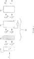
図1は、偏光検光子とともに色選択性偏光変調器を使用したフィルタを示す図である。
偏光子40は、一方の偏光状態が生じ、他の偏光状態が生じないホログラムであるホログラフィック偏光子でよい。ホログラフィック偏光子は、第1の偏光状態の光を偏向させ、他の偏光状態の光を偏向させない。偏光子40はEM Industries製のTransmax偏光子でもよい。
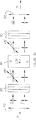
図2aおよび図2bからなる図2は、偏光検光子が中性偏光子と結合したリターダスタックを示し、(a)変調器の第1の切替状態で白を、(b)第2の切替状態でろ波されたスペクトルを透過するフィルタを示す図である。
図3aおよび図3bからなる図3は、偏光検光子が直線色偏光フィルタを示し、(a)変調器の第1の切替状態で白を、(b)第2の切替状態で黄を透過するフィルタを示す図である。
図4aおよび図4bからなる図4は、偏光検光子がコレステリック液晶であり、(a)変調器の第1の切替状態で白を、(b)第2の切替状態で黄を透過するフィルタを示す図である。
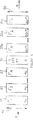
図5は図2に示すフィルタの通常白の実施形態を示す図である。
図6は図2のフィルタの通常ろ波状態の実施形態を示す図である。
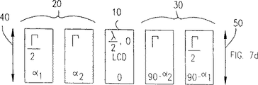
図7a〜図7dからなる図7は、合計(a)2つのリターダおよび(b〜d)4つのリターダを有するフィルタを示す図である。
図8はG/Wフィルタの測定透過率を示す図である。
図9はW/Cフィルタの測定透過率を示す図である。
図10はW/Mフィルタの測定透過率を示す図である。
図11はW/Yフィルタの測定透過率を示す図である。
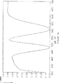
図12は、方位角0°に対しての入射角の関数として図10のW/Mフィルタの測定透過率を示す図である。
図13は、方位角90°に対しての入射角の関数として図10のW/Mフィルタの測定透過率を示す図である。
図14は、LCDに印加されたrms電圧の関数として図10のW/Mフィルタの測定透過率を示す図である。
図15は白/シアンフィルタ段の連続変調を示す図である。
図16は白/マゼンダフィルタ段の連続変調を示す図である。
図17は白/黄フィルタ段の連続変調を示す図である。
図18はマゼンダ/白フィルタ段の極限切替状態を示す図である。
図19は段間に偏光子を有する多重段フィルタを示す図である。
図20は内部偏光子を有しない青、緑および赤の変調段から構成されるフィルタを示す図である。
図21は特定の3段フィルタデザインを示す図である。
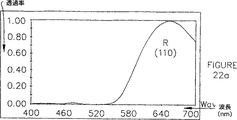
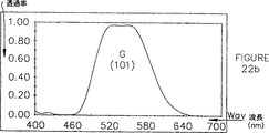
図22は、図21のフィルタの(a)赤出力、(b)緑出力および(c)青出力を示す図である。
図23は、図21のフィルタの(a)シアン出力、(b)黄出力および(c)マゼンダ出力を示す図である。
図24は、図21のフィルタの白、黒およびグレースケール出力を示す図である。
図25は、図25a〜図25cからなり、(a)3段フィルタの赤、緑および青透過スペクトル、および(b)段間の偏光子を使用して達成された暗状態および(c)内部偏光子を使用せずに達成された暗状態を示す図である。
図26は偏光独立多段フィルタを示す図である。
図27は入れ子偏光スタックを有するフィルタを示す図である。
図28は偏光検光子用のコレステリック液晶を使用した3段フィルタを示す図である。
図29は、第1および第2の配向ならびに第1および第2のリターダンスを有する第1および第2のリターダを含むスタックを示す図である。
図30aおよび図30bからなる図30は、図29のスタックに対応するスタックへの部分偏光入力の2つの一般的な例を示す図である。
図31aおよび図31bからなる図31は偏光子を追加したスタックを示す図である。
図32aおよび図32bからなる図32は、部分偏光を操作し、合成変調器出力光を出力するデバイスを示す図である。
図33aは少なくとも部分的に偏光した光を操作するデバイスを示す図であり、図33bは、部分的に偏光した光が楕円偏光した場合の図33aに対応する図である。
図34は従来技術の減色カラーフィルタを示す図である。
図35aおよび図35bからなる図35は、ねじれネマチック電気光学変調器を有するフィルタを示す図である。
図36は図35のフィルタを使用した3段フィルタを示す図である。
図37は、第3の原色に充てられた第2の段とともに2つの原色を時間的に多重化する第1の段を使用したインラインフィルタを示す図である。
図38は受動プリフィルタリングデバイスの一例を示す図であり、各ボックスはボックスの底部に示される角度で配向したリターダを示す。
図39はこのフィルタ上に入射した可視光の透過率を示す図である。
図40は、例えば図1に示される上記の色選択性偏光変調器を使用したダイレクトビュー(直視)ディスプレイを示す図である。
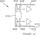
図41は、例えば図1に示される上記の色選択性偏光変調器を組み込んだリード実装ディスプレイシステムを示す図である。
図42は、例えば図1に示される上記の色選択性偏光変調器を使用した2光バルブシステムを示す図である。
図43は、本発明による2色シャッタディスプレイシステムの概略図である。
図44は、オーバヘッドプロジェクタ用のシャッタシステムの使用を示す図である。
好ましい実施形態の詳細な説明
本発明の色選択性偏光変調器を図1に示す。偏光変調器60はリターダスタック20とともに変調器10によって形成される。偏光変調器は偏光入力光を使用し、この場合偏光P0は偏光子40によって与えられる。偏光変調器は偏光検光子70と結合してフィルタを形成することができる。
図1に示すように、入射白色光はスペクトルFを有する光と相補(補色)スペクトルF(−)を有する光とが結合したものと考えられる。リターダスタック20はスペクトルFの光の偏光を変調器10の偏光PMの変調状態に変換し、スペクトルF(−)の光を偏光PIの等方状態に変換する。一方のスペクトルに対して、変換は恒等変換である。すなわち偏光は不変である。偏光PIの光は変調器10によって透過され、印加電圧とともに変化しない偏光を有する。偏光PMを有する光は印加電圧の関数として偏光PMに変調される。このようにすると入力光の一部の偏光は変調され、残部は変調されない。
変調器は、電圧の印加で透過光の偏光状態を制御するデバイスである。変調器は、変調偏光状態ならびに等方偏光状態を有する、すなわち透過偏光状態が変調器に印加された電圧に依存する入力光の偏光状態と、透過偏光状態が変調器に印加された電圧と実質上無関係である偏光状態がある。等方状態では、一般に偏光は不変であるが、いくつかのシステムでは、偏光は、直線偏光の90°回転や円偏光の左右像反転など、電圧と無関係の変換を有することがある。偏光および偏光状態なる語は交換可能に使用される。
ある部類の適切な変調器は、固定の配向および電圧制御リターダンスを有する電気光学可変リターダである。等方偏光状態は平行であり、かつ光軸に対して直角である。この場合それらはリターダの固有モード(Eigenmode)、または常波および異常波である。常偏光と異常偏光の間には電圧制御位相シフトがある。これはどちらかの等方状態の透過偏光に影響を及ぼすことはない。ただし、入力光が両方の等方状態に突出部を有するとき透過偏光は変化する。好ましい変調状態は、2つの等方偏光を二等分する直線偏光である。これは2つの等方状態に沿った突出部が等しい振幅を有するので最大変調深さを有する。均一に整合した電気制御複屈折(ECB)、ホメオトロピック配列(homeotropically)に整合した光学的に制御される複屈折(OCB)、ハイブリッド整合ネマチック(HAN)、およびπセル(pi-cell)/表面モードネマチックを含めて、ゼロねじれネマチックなど、LiNbO3、石英、および液晶を含む電気光学変調器はこのグループの電気光学変調器の好ましい実施形態の1つである。
光能動デバイスは適切な電気光学変調器の他のグループである。光能動デバイスは、その回転が入力光の偏光の配向に依存しない偏光回転子である。等方状態は左回りおよび右回りの円偏光状態である。変調器は、円偏光状態に影響を及ぼさない円偏光の電圧制御位相シフトを行う。ただし、円偏光の等しい振幅に分解できる直線状態では、透過偏光は直線偏光であり、配向は円状態間の位相シフトによって決定される。したがって、光能動変調器は直線状態に対して偏光回転子の働きをし、変調偏光状態はいずれかの直線状態である。
キラル・スメクチック液晶(CSLC)リターダは偏光を回転させるのではなく、軸を介して偏光を反射するが、それらはそれらの等方偏光状態および変調偏光状態において光能動デバイスと同様である。ゼロねじれネマチックと異なり、CSLCは印加電圧によって決定される固定のリターダンスおよび光軸配向を有する回転可能なリターダである。半波長リターダンスの場合、CSLCは円等方状態および直線変調状態を有する。CSLCの光軸の電圧制御配向は直線光の透過配向を決定する。
また、ねじれネマチックデバイスなど、中間変調および等方状態を有する電気光学変調器もある。ねじれネマチックデバイスは楕円固有偏光(Eigenpolarization)状態を有する楕円リターダであることが示されている。直線リターダと同様に、位相シフトは実質上偏光状態のある特定のヘリシティ(helicity)によって決定される(J.L. Pezzaniti and R.A. Chipman,(1993),「Phase-only modulation of a twisted nematic liquid-crystal TV by use of the eigenpolarization states」(固有偏光状態を用いたねじれネマチック液晶TVの位相のみの変調)Opt. Lett. 18, 1567-1569)
電気光学変調器中で使用される適切なネマチック液晶セルには、ねじれネマチック(TN)、スーパーねじれネマチック(STN)、電気制御複屈折(ECB)、ハイブリッド電界効果、πセルおよび表面モード、ゼロねじれモード、ハイブリッド整合ネマチック液晶リターダがある。適切なスメクチック液晶セルには、キラルスメクチック、強誘電性結晶、SmC*、表面安定化SmC*、体積安定化SmC*、バイナリSmC*、アナログSmC*、SmA*、エレクトロクリニック、ひずみヘリックス強誘電性結晶、反強誘電性結晶、フレキソエレクトリック(flexoelectric)結晶、およびアキラル強誘電性液晶リターダがある。対向するデバイス基板上に付着した透明電極ではなく、1つのデバイス基板上の横方向電極を使用した場合、ネマチック液晶は固定のリターダンスを有する回転可能なリターダとして動作し、スメクチック液晶は固定の配向を有する可変リターダとして動作する。
1つまたは複数の受動リターダとともに液晶能動リターダを使用した複合リターダが電気光学変調器中で使用されることがある。どちらも参照により本発明の一部となる米国特許出願第08/419593号に記載されているアクロマチック複合リターダおよび米国特許出願第08/549963号に記載されているアクロマチック偏光回転子は特に有用である。アクロマチック複合リターダは、受動リターダを側面に備えた液晶回転可能半波長リターダを含み、受動リターダの配向およびリターダンスは複合リターダがアクロマチックになるようなものである。アクロマチック偏光回転子は、受動半波長リターダとともに液晶回転可能半波長リターダを含む。
リターダスタックと電気光学変調器との適合性を得るために、受動リターダを電気光学変調器中に入れることができる。例えば、リターダスタックが45°だけ分離した2つの直線偏光中の光を作った場合、固定の配向を有する可変リターダに対する変調偏光状態および等方偏光状態が生じる。一方の偏光状態に対して平行に配向した受動4分の1波長リターダは、2つの直線偏光を1つの直線偏光と1つの円偏光に変換する。これらは固定のリターダンスを有する回転可能リターダに対する変調偏光状態および等方偏光状態である。したがって、電気光学変調器が受動4分の1波長リターダをCSLCの両側に含んでいる場合、可変リターダ用に設計されたスタックが回転可能リターダとともに使用できる。
リターダスタック20は1つまたは複数の受動リターダを含む。リターダがN個ある場合、配向はα1〜αNであり、リターダンスはΓ1〜ΓNである。任意のリターデーション材料がリターダスタック中で使用できる。リターダ材料は、高い光学的清澄性、均一なリターダンス、設計要件に対して十分なリターダンスの範囲(これは誘導される複屈折の範囲および厚さの実際的な範囲に依存する)、環境耐久性、および多くの場合、大面積および低コストを与えることが好ましい。
リターダスタックは、例えば、複屈折性デバイス、液晶ポリマーフィルム、延伸ポリマーリターダシート、または結晶リターダの形の層を使用して構成できる。延伸ポリマーフィルムは、独特の複屈折分散特性を有する様々な材料を使用して、任意のリターダンス(0〜2,000nm)のものが得られる。大きいシートが低い価格で購入でき、大きい透明なアパーチャフィルタが可能になる。z延伸ポリマー(Nitto NRZ)の特性は小さいリターダンスシフトとともに大きい視野角を可能にする。ポリビニルアルコール、ポリカーボネート、マイラー、ポリプロピレン、ポリスチレン、トリアセテート(トリブチルアセテート)、ポリメチルメタクリレートを含めて、他のいくつかのポリマー材料がフィルタの製造に有用である。ただしこれらに限定されない。
液晶ポリマーフィルム、特にUV架橋可能ポリマーネマチック直線リターダはリターダスタックを形成するのに特に適している。魅力的な特徴は、その材料が非常に高い複屈折を有するので薄い高次のリターダを製造できることである。したがって単一の基板上に多層スタックを低いコストで製造することができる。液晶ポリマーは、2つまたはそれ以上のリターダを含むリターダスタックを製造するのに特に好適である。液晶ポリマー層を製造するためには、まず整合層を基板上に付着し、次いで偏光で光重合させる。偏光の配向が、整合層と続いて付着される液晶ポリマー層の配向を規定する。光重合光の偏光は容易に制御されるので、液晶ポリマーリターダのスタックをスタック中の各リターダの制御された整合とともに製造できる。これは、シートリターダの整合がより困難である斜めの相対配向、すなわち0°または90°以外の相対配向に対して特に有利である。
石英、マイカ、方解石など、従来の結晶リターダ材料は、ポリマーフィルムで実現可能なよりも高い解像度を必要とする用途に好適である。それらはまた、低い波面ひずみおよび/または高い出力処理要件を必要とする用途に有用である。それらはポリマーリターダよりも費用がかかり、特に低いリターダンスが必要なとき大面積に適していない。
ポアンカレの球分析を使用して、変調器が0°または90°で直線偏光である等方状態および±45°で直線偏光する変調状態を有する場合(例えばゼロねじれネマチックZTN)についてリターダの適切な配向を計算した。すべてのリターダが同じリターダンスを有する場合、配向は次式によって関連付けられる。
αN−αN-1+...α2−α1=π/8+πm/4 式1
上式でmは整数である。例えば、リターダが1つの場合、m=0、1、2、...に対してπ/8、3π/8、5π/8、...で配向する。リターダが2つの場合、α1が選択された後、α2が決定される。例えば、α1=π/16に対して、式1はα2=3π/16+πm/4を与える。これはm=0の場合3π/16となる。配向は、リターダが3つ以上の場合同様に決定される。また、ポアンカレの分析を使用して、等方偏光および偏光変調の他の選択に対してリターダ配向を計算することができる。
偏光変調器60と偏光検光子70を組み合わせると、図1にF%で示される出力を有する第1のスペクトルを強度変調するが、スペクトルF(−)に対しては一定の出力を有するフィルタが形成される。検光子に応じて、F(−)の出力は0%と100%の間のどこかで固定される。偏光検光子は偏光子と組み合わせた第2のリターダスタックである。第2のリターダスタックは、検光偏光子がスペクトルF(−)に対して等方性であるときは不要である。したがって、直線または円色偏光フィルタを偏光検光子として使用できる。
偏光検光子が第2のリターダスタックを含むフィルタを図2に示す。これは第1のリターダスタック20と第2のリターダスタック30の間に配置された変調器10によって形成される。変調器は、変調器のある切替状態では2つのスタックが協働して入力光のスペクトルをろ波し、他の切替状態ではリターダが実質上消え、ろ波されていない、または白い出力スペクトルが生じるように第2のスタックの見かけの配向を変化させる(図2a)。
フィルタは、入力偏光子40、および中性(neutral)偏光子である検光偏光子50を含む。配向角は入力光の偏光に対して定義され、この場合偏光子40によって定義される。光源が偏光を与える場合、入力偏光子は不要である。フィルタは検光偏光子の働きをする別個の偏光デバイスと結合できる。この実施形態では、フィルタは直線偏光子とともに示されている。一般に、それらは直線、円または楕円偏光子である。適切な偏光子には、吸収偏光子、二色性偏光子、染料ベース偏光子、非吸収性偏光子、偏光誘電フィルム偏光子、偏光ビームスプリッタ偏光子、方解石偏光子、石英偏光子、散乱偏光子、プリズマティック偏光子、コレステリック偏光子、スタックコレステリック偏光子がある。偏光子は、直線偏光と円偏光を変換する4分の1波長リターダなど、追加の偏光調整要素を含むことができる。
フィルタは(a)半波長リターダンスと(b)ゼロリターダンスの間で切り替えられるゼロねじれネマチック変調器とともに示されている。リターダは、上部に示されるリターダンスおよび底部に度で示される入力偏光に対する配向とともにボックスで表される。リターダは設計波長での指定されたリターダンスを有する。設計波長は、一般にフィルタの動作範囲内に入り、フィルタ性能を最適化するように調整できる。本明細書に示されるすべての配向は近似的であり、フィルタ出力を調整するために数度だけ調整できる。
図2のフィルタでは、変調器10は、0°で配向し、電界が印加されない(「オフ」)ときのλ/2と十分に(「オン」)の電界が印加されたときの理想的な0との間で変化するリターダンスを有する電気光学ゼロねじれネマチック液晶である。この変調器の場合、等方状態は0°または90°で直線偏光であり、変調状態は+/−45°で直線偏光する。この実施形態では、変調器は液晶ディスプレイ(LCD)である。ここでLCDなる語は、1つまたは複数のピクセルを有する液晶セルを含む任意の液晶デバイスを表すために使用される。LCDは一般に、各ピクセルが独立して制御される液晶セルの多重ピクセルアレイである。フィルタは多重ピクセルLCDまたは非ピクセル化電気光学変調器とともに実施できる。LCDの単一のピクセルのリターダンスを図2に示す。
図示の実施形態では、白色光は偏光器40上に入射する。可視スペクトル外で動作するように設計されたフィルタの場合、「白色」光は光のすべての入力波長であり、例えば赤外波長分割多重化ではそれはすべての赤外チャネル波長になる。白色光はFで示される第1のスペクトルおよびF(−)で示される第2の相補スペクトルから構成されると考えられる。
スタック20中のリターダは、スペクトルFが45°直線偏光の変調状態で出力または透過され、かつスペクトルF(−)が0°直線偏光の等方状態で出力または透過されるようなリターダンスおよび配向を有する。第1の切替状態(図2a)では、変調器はリターダンスλ/2を有することが理想的であり、それにより変調状態を生じるスペクトルの偏光が−45°に切り替えられる。等方状態は不変である。第2の切替状態(図2b)では、変調器はゼロリターダンスを有し、変調器から出力された光の偏光は変調状態ならびに等方状態に対して不変である。
第2のリターダスタック30の後に変調器がある。変調器が第1の切替状態にあるとき、第2のスタックは第1のスタックの変換を元に戻し、それにより0°で直線偏光したFならびにF(−)を透過する。偏光子50は両方のスペクトルを透過し、フィルタ出力は白色光になる。第2の切替状態では、第2のスタックは、FならびにF(−)を直角に偏光させる変換を完了する。偏光器50はスペクトルFを有する光を阻止し、出力はスペクトルF(−)を有するろ波された光になる。偏光器50が90°で配向した場合、フィルタは白およびF(−)の相補(補色)である黒とFスペクトルの間で切り替わることにある。出力は変調器が「見え」ない第2の状態でろ波されるので、フィルタは正常ろ波(NF)と呼ばれる。LCDを取り外した状態でスペクトル全体を透過(または阻止)するフィルタは正常白(NW)と呼ばれる。一般に、正常状態は原色/白/または白/原色フィルタを名前付けする際に最初に記載されるが、白/原色なる語はまたどちらに対しても総称的に使用される。
好ましい実施形態では、フィルタはカラーフィルタであり、スペクトルFおよびF(−)は加法混色の原色(赤、緑、または青)および相補の減法混色の原色(シアン、マゼンタ、または黄色)に対応する。FスペクトルまたはF(−)スペクトルのどちらが加法混色の原色であってもよい。したがって、可視範囲では、フィルタは平行偏光器に対しては原色/白フィルタになり、交差偏光器に対しては原色/黒フィルタになる。フィルタは一般に、ろ波されたスペクトルが原色スペクトルに限定されない白/ろ波スイッチとして使用できるが、ここではカラーフィルタリングの場合について一般的に述べる。このフィルタは、それが変調するスペクトルではなくそれが透過するスペクトルに対して名前付けされる。したがって、図2のフィルタは、それが例えば電気光学変調器によって変調されたFスペクトルであってもF(−)/Wフィルタになる。
ポリマーは、2つまたはそれ以上の小さい分子が結合してより大きい分子を形成する化学反応によって形成される反復構造単位から構成される化合物または化合物の混合物である。
液晶ポリマー(LCP)は、液晶モノマーが主鎖(背柱)の沿ってまたは側鎖単位として高分子構造中に組み込まれたポリマーの一種である。
LCPは、機械的に摩擦された表面、せん断、またはごく最近開示された光学的手段によって整合できる。光学的方法は、まず直線光重合(LPP)フィルムまたはアゾベースの染料のどちらかをポリマー整合層中に加えるステップを含む。前者(Schadt他、Jpn. J. Appl. Phys. Vol.34, pg.3240-3249, 1995参照)の場合、LPP材料を基板上に付着し、その後に加える高い温度で硬化させる。次いで、硬化したフィルムを偏光UV光に当てる。次いで、LCPを同じ基板上にスピンオン(spun-on)またはコーティングし、LPPフィルムの配向と整合する。次いで、LCPを非偏光UV光に曝して架橋させる。後者(Shannon他、Nature, vol. 368, pg. 532-533, 1994)の場合、アゾ染料分子をポリイミド整合層(または複数の層)中に挿入し、それらを様々な基板(ガラス、シリコンなどを含む)上に付着する。液晶モノマーまたはポリマーを1つの基板上に付着するか、または2つの基板間に挿入する。LC分子ディレクタは、前に整合層と照明した偏光VU光の方向に対して直角に配向する。後の露光で液晶は再配向する。これは用途によっては不利益になる。
図2に変調器の2つの極限切替状態を示す。LCDピクセルが0またはλ/2以外のリターダンスを有する場合、F(−)スペクトルはまだ0°偏光配向を保持しており、完全に透過される。しかしながら、Fスペクトルの光は、0%(図2b)と100%(図2a)の間にある0°偏光状態に突出部を有する楕円偏光に変換される。したがって、変調器電圧のアナログ制御はFスペクトルのアナログ変調を与える。
検光偏光子用の色選択制偏光(CSP)フィルタ、例えば多色染料偏光子を図3に示す。光伝搬は矢印で示され、上部に示される色と底部に示される配向を有する。図示の特定の実施形態では、リターダスタック20は0°で青色光を、45°で黄色光を作る。電気光学変調器10は、0°での直線が変調され、45°での直線偏光が等方性である45°で配向したZTNである。検光偏光子80は、0°で黄色光を透過し、90°ですべての波長を透過する90°で配向した黄色(CSP)である。ZTNが半波長リターダンスを有するとき(図3a)、青色光は90°に回転し、(CSP)フィルタによって透過される。ZTNがゼロリターダンス(図3b)を有するとき、青色光は0°のままであり、(CSP)によって透過される。中間リターダンスでは、青色透過率は0%から100%の間で変化する。
円色偏光子、この場合コレステリック液晶(CLC)またはCLCポリマーを有するフィルタを図4に示す。リターダスタック20は45°で青色光を、0°で黄色光を透過する。電気光学変調器10は0°で配向し、かつ3λ/4(図4a)とλ/4(図4b)の間で切替可能なリターダンスを有するZTNである。45°での青色光の場合、したがって、偏光は左回り円偏光と右回り円偏光の間で変調される。中間リターダンスでは、中間楕円偏光が生成される。成分90は、右回り青色光を反射し、左回り青色光を透過し、偏光にかかわらず他の波長を透過する右回り青色CLCである。CLCは非透過偏光を吸収するのではなく反射するので、このフィルタは透過モードならびに反射モードで可変青色出力を与える。
この説明の残部は主として2つのリターダスタックフィルタを対象とするが、そのほとんどは任意の検光子に対して一般化できる。第2のスタックが第1のスタックの変換を元に戻すために、2つのスタックのリターダは、正常白フィルタについて図5に、正常ろ波フィルタについて図6に示されるように互いに関連付けられる。どちらの図でも、変調器10は、それが見えない切替状態で示されており、したがってフィルタの正常透過を示す。第1のスタックは、リターダンスΓ1、Γ2...ΓNおよび配向α1、α2...αNを有するリターダ21、22および23を有する。リターダンスが等しい場合、配向は式1に従って関連付けれられる。第2のスタックは、第1のスタックと同じリターダンスを有するが、順序が反対のリターダ33a、b、32a、bおよび31a、bを含む。第2のスタックのリターダは、NWの場合は90+αNの配向、NFの場合は90−αNの配向まで第1のスタックに対して回転する。NW構成では、第1スタックおよび第2スタックジョーンズ行列は互いに逆である。
変調器10が半波長リターダンスに切り替わったとき、NW構造はろ波スペクトルを与え、NF構造は色スペクトルを与える。LCDが完全にアクロマチックの場合、図5のフィルタは切替状態では図6のフィルタと同じスペクトルを与え、逆もまた同様である。NW構成とNF構成の主要な違いはLCDの色効果の結果である。NW構成では、白状態が理想的であるが、LCDの色度はろ波状態の色コントラストを劣化されることがある。NW減色白/原色フィルタ(W/C,W/MまたはW/Y)の場合、LCDは変調された加法混色の原色(R、GまたはB)の帯域幅にわたってアクロマチックであるだけでよい。逆に、W/R、W/GまたはW/BフィルタのNW設計は、LCDが変調減法混色の原色の帯域幅にわたってアクロマチックであるとき、最も良い結果をもたらす。LCDは、例えば変調帯域内にLCD設計波長を備えることによって、変調帯域の切替のために最適化されることが好ましい。これは、変調帯域が赤帯域ならびに青帯域を含む減法混色の原色のマゼンタである正常白W/Gフィルタにとって難しい課題である。
NF構成では、白状態に色度の問題が生じることがある。ただし、少なくとも1つの加法混色の原色帯域は常にLCDリターダンスにかかわらず透過されるので、LCDリターダンスは変調減法混色の原色帯域を最適に通過するように選択できる。白状態での色度は、白状態でのスループットの結果として生じる損失がろ波状態での漏れよりも色品質に大きな影響を及ぼさないので、ろ波状態の場合よりも有害ではない。したがって、色度の点で、G/wフィルタはW/Gフィルタよりもよく動作する。
有用なスタック設計は、制約に自然に適合するように計られた構造を有するSolcまたはスプリットエレメントフィルタなどフィルタ設計から始めることによって生成できる。あるいは、有用な透過スペクトルを有するフィルタ設計は、例えばネットワーク統合技法(すべて参照により本発明の一部となるHarris他(1964), J. Opt. Soc. Am. 54:1267; Ammann他(1966), J. Opt. Soc. Am. 56:1746; Ammann(1966), J. Opt. Soc. Am. 56: 943;および1995年5月23日に出願された米国特許出願第08/447522号参照)を使用して生成し、次いで設計要件に一致するサブセットについてスクリーニング(選別)できる。第3の手法は、有用なスペクトルプロファイルを有するものを見付け出すために設計要件に適合するすべての設計を組織的に評価することである。
この第3の手法を図7に示す。図示のフィルタは図6のNF設計要件に従う。LCD変調器は2つのリターダンス間で切替可能であり、どちらもコンマによって記載され、分離される。アナログ変調器の場合、リターダンスはこれらの極限値間で連続的に調整できる。図7aは、合計2つのリターダについて各スタック20および30中にただ1つのリターダを有する最も簡単なフィルタ設計を示す。図7b〜図7dは、それぞれ合計4つのリターダを有する設計を示す。正常状態で、α2=45°が成り立つ特殊な場合、それはリターダンス2Γ2および配向45°を有する中央リターダを有する3リターダフィルタと等価である。
図示のフィルタでは、各スタック中のリターダは、等しいリターダンスを有するか、または2分の1だけ異なるリターダンスを有し、したがって実数インパルス応答関数を生じる。これは必要条件ではなく、リターダンスは関連付けられず、したがって複素インパルス応答関数を生じる。等しいリターダンスは製造を容易にする。これらの例は有用な設計の完全な組ではない。それらは単に、加法混色の原色帯域または減法混色の原色帯域の有用なフィルタを生じる構造の1つのグループを示す。
図7に基づくフィルタ設計は、α1(5、10、15、20...)の値を増分し、αの各値ごとに、α2の値を増分することによって生成した。各フィルタの透過スペクトルを計算し、有用なスペクトルを特定した。スペクトルは、ミュラー行列またはジョーンズ行列を使用して計算できる。ディスプレイ用途にとって好ましいスペクトルは、所望のスペクトルに一致する衝撃係数(duty ratio)を有し、長方形に見えるプロファイルを有する。フィルタは、急峻な遷移勾配、ならびに比較的平坦な透過帯域および比較的平坦な阻止帯域を有することが好ましい。比較的平坦な帯域は、スペクトル中に一連の分散した高コントラストのゼロまたはピークを備えることによって達成できる。ほぼ理想的な透過スペクトルはリターダの数を多くすることによって生成できる。実際問題として、容認できる遷移勾配およびサイドローブ振幅/位置は、有限数の構成要素とともに彩度を最適化するように慎重に選択しなければならない。
フィルタ解像度は、原色帯域にわたってピーク透過率を維持するために十分に低くなければならない。彩度の観点から、通過帯域解像度は、所望の原色帯域のみを分離するために十分に高くなければならない。急峻な遷移勾配(または通過帯域中の複数のピーク)とともに、十分に低い解像度をつくり出す設計が好ましい。
有用な設計の一部を表Iに示す。両方のスタックのリターダは、LCDが見えない正常切替状態でそれらが現れるように表に記載されている。リターダの合計数Mが記載されている。リターダンスが等しい場合、配向は式1に従うことに留意されたい。α1およびα2を進むことによって得られる適切な設計は角度の微調整によって改善できる。基本設計を特定した後、所望の減法または加法混色の原色変調をつくり出すようにリターダンスΓを選択できる。
ファンSolcフィルタは、図6の設計要件に偶然一致する構造のファミリーである。この一致は偶然の一致であり、Solc設計の意図的な特徴ではない。Solcフィルタは、参照により本発明の一部となる1996年6月11日出願のU.S.P.N.5469279号および米国特許出願第08661498号に記載されている。Solcフィルタは、それぞれファン設計および折り畳み設計に対して設計波長で全波長リターダまたは半波長リターダになる一連の等しい厚さのリターダを必要とする。ファンSolcフィルタの場合、リターダはα、3α、5α、...(すなわちαN=(2N−1)α1)で配向する。折り畳みSolcフィルタの場合、それらは交番するロッキング角α、−α、α、...(すなわちαN=(−1)N+1α1で配向する。
表IIはこれらの要件に従うSolc設計を示す。ファンSolc設計は図6の要件に偶然適合することに留意されたい。Mが奇数のとき、ファンSolc設計の中央リターダは45°で配向し、この角度では角α=90−αが成り立つ。したがって、中央リターダは単に半分に分割され、半分は各リターダスタック中に入れられる。リターダの合計数Mは、正常状態で中央の2つのリターダが単一のリターダと等価である場合について”3”や”5”のように引用符で記載されている。リターダ配向は、α=π/4Mが成り立つ場合、リターダの合計数の関数である。
ファンSolcフィルタの場合、フィルタは本発明の白/原色フィルタの基準に自然に適合する。一方、折り畳みSolcフィルタは本発明の基準に適合しない。リターダンスはこの制約を満足するが、配向はαN=90±αNに従わない。折り畳みSolc設計は、表IIIに示すようにこの基準を満足する準折り畳みSolc設計に修正できる。準折り畳みSolc設計なる語は、リターダがすべて同じリターダンスを有し、かつ各スタック内で、それらがすべてほぼ同じ角度で、ただし交番する符号で配向するすべての設計に対して使用される。
ファンフィルタと同様に、代表的な折り畳みSolcフィルタでは、α=π/4Mが成り立つ。例えば、N=6のリターダを有する代表的な折り畳みSolcフィルタはα=8°を必要とする。準折り畳みSolcフィルタの場合、角αに対する制限はない。表IIIに示すように、角αは、まだ有用なスペクトル応答を生成している間に大きく変化する。表I〜表IIIはNF設計を示す。NW設計を作るためには、第2のスタック中の各リターダの角度の符号を反対にする。
Solcフィルタと同様に、スプリットエレメントフィルタは図5および図6の要件に自然に適合する。カラーディスプレイに適したスプリットエレメントフィルタは、全体として参照により本発明の一部となるU.S.P.N.5528393号に記載されている。これは、入射偏光に対して±45°で配向した第1および第2のリターダンス一致スプリットエレメントリターダ、および0°で配向した中央リターダを含む。平行スプリットエレメントの場合、フィルタはNFになり、交差スプリットエレメントの場合、それはNWになる。
本発明の白/原色フィルタを形成するために、スプリットエレメントリターダはスタックを形成し、中央リターダはLCDとスプリットエレメントリターダの1つとの間に配置できる。この非対称の場合、LCDの両側のリターダは一致しないが、スタックはそれぞれ単一のリターダを含むと考えられ、スプリットエレメントリターダおよび中央リターダはどちらのスタック中にも含まれない追加の要素と考えられる。中央リターダは電気光学変調器に対して平行または直角に配向するので、対称性がないことは白切替状態の達成を妨げない。言及した実施形態を表IVに示す。この表では、中央リターダはスタック1リターダに沿って記載されている。図示のリターダンスでは、フィルタ透過率は2段ライオットフィルタに近い。各スプリットエレメントリターダに加えられた4分の1波長リターダンスのために、この設計は複素インパルス応答フィルタの組に属する。
上述のすべての設計では、配向を最適なプロファイルが得られるように選択した後、次いで各原色で最適な色彩度が得られるようにリターダンスを選択した。この設計パラメータは、特定のリターダ材料に適合した分散を含む標準のミュラー行列技法を使用して分析できる。フィルタ設計を評価する基準は、彩度、色相、スループットの考慮に基づく。彩度および色相はCIE色度図を使用して評価できる。特定のフィルタ出力によって生成される色の品質は、特定のフィルタ状態の透過関数、光源のパワースペクトル、およびCIE等色関数を含めて、一連の重なり積分を計算することによって特徴付けられる。
純原色は、所望の原色帯域中で透過した光源パワーと原色帯域外で透過した光源パワーとの比を最大にすることによって生成される。フィルタ設計は、最適化を全く明確にするために光源特性に一致させることができる。例えば、6000K黒体など真の白色光源は、CRT発光体など分散光源よりもフィルタ性能により大きい負担をかける。阻止帯域中のゼロのスペクトル位置は構成要素のリターダンスに依存する。ゼロを戦略的に光源の帯域外パワースペクトル最大値に置くことが有利である。同様に、サイドローブ最大値を帯域外パワースペクトル最大値から離れたところに置くことが有利である。受動フィルタを挿入して、原色帯域外にある帯域を除去すれば、彩度を高めることができる。
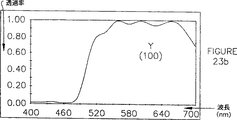
白/原色フィルタの測定スペクトルを図8〜図11に示す。フィルタの構造は表Vで与えられる。スイッチは、表に記載されている付勢されていない半波長リターダンス中心波長を有する3TNセルを使用する。偏光子はハードことのみを有するNitto−Denko(日東電工)製のEG1425である。したがって、透過率は2つのフレネル損失を含む。リターダは、それぞれ表に記載されている設計リターダンスを有するNRZリターダのシートである。NW設計の場合、白状態での損失は、偏光子、LCD上のITO電極による吸収、外部反射、およびLC残留リターダンスに関連する。後者は一般に約20nmである。スペクトルは、ANDO光スペクトル検光子を使用して走査し、平行グラントムソン偏光子を使用して光源スペクトルによって自動的に正規化した。
受動リターダおよびLCDリターダの設計波長は表Vで与えられる。能動リターダならびに受動リターダでは、設計波長はリターダが指定されたリターダンスを与える波長である。受動リターダの場合、設計波長は、受動リターダが2λリターダになるW/Mフィルタを除いて、受動リターダが全波長リターダになる波長である。リターダスタック設計波長は、変調された阻止ピークが所望の色帯域中にくるように選択される。LCDの設計波長は、リターダンスが付勢されていない状態でλ/2になる波長である。LCD色度の影響を最小限に抑えるために、設計波長を変調帯域の中央にくるように選択することに留意されたい。
G/Wフィルタ、W/CフィルタおよびW/Mフィルタは準折り畳みSolc設計である。G/W設計は表IIIの第3の設計と同じである。W/M設計は表IIIの第2の設計と同じであるが、正常ろ波ではなく正常白なので、第2のスタック中のリターダの配向は反対の符号を有する。W/C設計では、リターダの配向は遷移の急峻さを高めるために調整されている。W/Y設計は、表Iの第5の設計と考えられ、リターダンスΓ=2λが成り立つ。
図8〜図11のフィルタスペクトルの優れた通過帯域透過、阻止帯域阻止、および急峻な遷移エッジに留意されたい。青のフィルタ透過率の低下は、青の損失を有するシート偏光子を使用したためであり、リターダ/フィルタ設計のためではない。透過率は改善された偏光子を使用すれば改善できる。
本発明の利点は、LCDが色シフトを誘導する機構を有しないことである。すなわち、遷移帯域幅はLCDの状態と無関係にリターダスタックによって定義される。したがって、視野角(またはLCD色度)の変化はフィルタ透過率にほとんど影響を及ぼさない。スタックによって定義される遷移帯域中心波長などの特徴は、スタックが角度依存である範囲まで保持される。視野角の変化は、阻止された色の密度のわずかな損失のみを生じ、帯域位置にシフトを生じない。
このことは、図10のW/Mフィルタで実証される。方位角が0°の場合について、入射角による透過率の測定変化を図12に示す。垂線から−50°にもわたる入射角に対して、スペクトルが不変であることは注目すべきことである。マゼンタ透過率はわずかに低下するが、緑阻止は優れたままであり、帯域位置は不変である。青/緑遷移および赤/緑遷移の半最大値(half-max)はスタックによって固定される。スペクトルは方位角ならびに入射角とともに変化する。測定した最悪の方位角は、図13に示すように90°である。0°入射角透過率は、実際にはどちらかの方位角に対して同じであり、図12および図13の測定上の違いは、光ファイバを介した光源の偏光依存結合のアーチファクト(artifact)である。方位角90°の最悪の場合でも、阻止密度は優れており、帯域はシフトしない。このことは優れた広視野角色スイッチおよびディスプレイシステムに役立つ。
本発明に基づく減色ディスプレイの固有の機能は、未変調の原色の透過に影響を与えずに、変調済みの光の透過のグレーレベル制御にアナログLCDを使用できることである。これは、図14、すなわち、図10のW/Mフィルタの実験的に測定された出力に示されている。いくつかの異なる駆動電圧での透過スペクトルが示されている。フィルタは通常、白であり、したがって、零リターダンス状態(10V)のすべての波長を完全に透過させる。リターダンスが増加するにつれて、変調済みの原色、すなわち、緑色の透過は、半波長リターダンス状態(0V)で最小限に抑えられるまで次第に遮断されていく。フィルタは、マゼンタ色光に影響を与えずに緑色光の独立の変調を示す。
W/Cフィルタ、W/Mフィルタ、W/Yフィルタの場合のグレースケール変調がそれぞれ、図15〜図17に示されている。加法混色の原色R、G、Bの透過は、相補減法混色の原色とは完全に独立に制御される。これらのフィルタの設計は、表VIの最初の3つのエントリに与えられている。リターダはNitto Denkoポリカーボネートフィルムである。光変調器は、0°でゼロねじれネマチック配向され、零リターダンスと半波長(π)リターダンスとの間で連続的に変動する。ネマチックの平面外傾斜角はスペクトル内に示されており、0°は半波長リターダンスに対応し、75°はほぼ零リターダンスに対応する。90°はより零リターダンスに近いが、表面ピニング効果のためにこれを達成するのは困難である。
M/Wフィルタは、図18に示されており、表VIの1番下にリストされている。これはスプリットエレメントフィルタであり、中央リターダが第1のスタックを備える。このフィルタでは、LCDが0°ではなく90°に配向される。他のフィルタでは、リターダの配向が0°の場合も90°の場合もフィルタ関数は同じである。スプリットエレメント設計の場合、非対称性のために、スペクトルは同じではない。ただし、2つの配向は共に機能的である。この特定のフィルタでは、2つの配向を評価したところ、90°配向の方がより優れた出力を与えることがわかった。このフィルタは、図18に示した2つの互いに逆の切替え状態の間で連続的に変化させることができる。このフィルタはNFであるので、白色スペクトルは色度の影響を受ける。
本発明の減色フィルタの固有の特性は、図15〜図17に示されているように、未変調のスペクトルFが、Fスペクトルの電圧制御変調とは独立に完全に透過することである。そのため、それぞれ、他の2つ加法混色の原色に影響を与えずに1つの加法混色の原色の独立のアナログ制御を可能にする、2つ以上のフィルタ段を直列に使用することができる。1つの段フィルタは2つの出力、すなわち、加法混色の原色または減法混色の原色と、黒(交差偏光子)または白(平行偏光子)とを有する。2段フィルタは、4つの出力、すなわち、3つの原色(2つの加法混色の原色と1つの減法混色の原色、または1つの加法混色の原色と2つの減法混色の原色)と、黒または白とを与えることができる。3段フィルタは、8つの出力、すなわち、3つの加法混色の原色と、3つの減法混色の原色と、黒および白とを与えることができる。変調器がアナログである場合、フィルタは極色同士の間のグレースケールを与えることもできる。複数段フィルタでは、1996年11月25日に出願され引用によって本明細書に全体的に組み込まれた米国特許出願第08/758122号に記載されたように色度を低減することができる。複数段フィルタは、1996年5月14日に出願され、やはり引用によって本明細書に全体的に組み込まれた米国特許出願第08/645580号にも記載されている。
図19に示したように、各段で入口偏光子および出口偏光子を使用してフィルタ同士を組み合わせることができる。この場合、フィルタ出力は、個々の各段の出力の積である。第1の段は、リターダスタック20aおよび30aと、LCD10aと、偏光子40aおよび50aとを備える。n個の段があり、各段の間に偏光子があり、n番目の段で終わり、この段はリターダスタック20nおよび30nとLCD10nと偏光子40nおよび50nとを備える。各段の出力偏光子は、次の段の入力偏光子として働く。たとえば、2つの段しかない場合、50aと40nは同じ偏光子になる。
フィルタ段とその相対的な配向を適切に選択することによって、図20に示したように、各段の間の内部偏光子を必要とせずに2つ以上の段を組み合わせることが可能である。偏光子は光損失の主要な原因となる恐れがあるので、内部偏光子を有さない複数段フィルタでは、特に反射モードカラースイッチおよびディスプレイの場合にスループットを著しく増大させることができる。
図20の3段フィルタは、偏光子40と偏光子50との間に配置された、青色光、緑色光、赤色光を独立に変調する段を有する。この実施形態では、第1の段は青色光を変調し、したがって、W/Yフィルタ段とY/Wフィルタ段のどちらかである。この段は、第1のリターダスタック20aと、第2のリターダスタック30aと、LCD10aとを備える。リターダスタックおよびLCDは本発明の任意の設計のものでよい。第2の段は、リターダスタック20bおよび30bとLCD10bとを備え、緑色光を変調し、したがってW/MフィルタまたはM/Wフィルタである。第3の段は、リターダスタック20cおよび30cとLCD10cとを備え、赤色光を変調し、したがってW/CフィルタまたはC/Wフィルタである。
特定の3段フィルタが図21に示されている。これらは、図9〜図11に示したのと同じフィルタ段であるが、内部偏光子なしで直列に組み合わされる。出力色は表VIIに与えられている。各段で、0は非励磁(変調)LCD状態を指し、1は励磁(等方)状態を指す。すべての3つの段が変調状態であるとき、第1ブロックが青を遮断し、第2ブロックが緑を遮断し、第3ブロックが赤を遮断し、そのため、平行な入力偏光子および出力偏光子と共に使用すると黒色出力が得られる。第3段のLCDは、等方状態に切り替えられるともはや赤色を遮断せず、フィルタ出力は赤になる。すべての3つのLCDを等方状態に切り替えると、出力は白になる。
白色出力は、赤、緑、青のサブピクセルが組み合わされて白を形成する、空間多重化されたフィルタまたはディスプレイ、あるいは画素の出力が赤と緑と青との間で切り替えられて白を形成する、時間多重化されたフィルタまたはディスプレイの3倍明るい。本発明のフィルタでは、空間および時間全体にわたって完全な白スペクトルを透過させることができる。
一般に、偏光子が並列するのでなく交差する場合、相補スペクトルが得られる。たとえば、並列偏光子を有するシアン/白フィルタの代わりに、交差偏光子を有する赤/黒フィルタでもよい。3つの段を内部偏光子なしで縦続接続する場合、交差偏光子を用いた場合でも白状態を達成することができる。内部偏光子で色が遮断されることがないので、直交軸上で完全な相補スペクトルを得ることができる。交差偏光子出力は表VIIに含まれている。状態(000)は黒ではなく白を与え、(001)は赤ではなくシアンを与え、以下同様である。
交差偏光子フィルタの利点は、黒状態の光学濃度が向上することである。黒状態が出力されるのは、すべての3つのLCDが、励磁等方切替え状態であり、したがって最小色度を有するときである。一般に、黒状態での遮断を強化することと引き換えに白状態でのスループットをある程度喪失させることが好ましい。
交差偏光子を有する図21のフィルタについては、加法混色の原色出力が図22に示されており、減法混色の原色が図23に示されている。すべての6つの原色の優れたスペクトルが単一のフィルタによって与えられ、得られる各原色がアナログ制御される。また、図24に示したように、白出力、黒出力、グレー出力が与えられる。0°〜75°の傾斜角が示されており、これらはλ/2ないし零よりわずかに大きな値のリターダンスに対応する。優れた黒状態が達成されることに留意されたい。図24に示したように、可視スペクトル全体にわたってグレースケール変調を達成するには、すべての3つのLCDの傾斜角を同時に変化させる。
内部偏光子をなくすと、各スタックに、協働して原色間帯域を遮断させることにより、並列偏光子を用いて黒状態を向上させることができる。あるいは、交差偏光子を用いた場合に白状態でのリプルが低減する。このことを理解するために、C/WスイッチとM/WスイッチとY/Wスイッチとからなる減色ディスプレイまたはカラーシャッタについて考える。任意に、黄色段およびマゼンタ段の遷移帯域と、マゼンタ段およびシアン段の遷移帯域を得て、半最大透過点で重ね合わせる。個々の加法混色の原色スペクトルは図25aに示されている。
最初に、図19に示したように、各スイッチの間に並列中性偏光子がある場合について考える。中性偏光子は各段を分離するので、黒状態は、各段によって生成されるCスペクトル、Mスペクトル、Yスペクトルの積である。各スペクトルが半最大透過点で重なり合うので、図25bに示したように、遷移帯域の中心での漏れは25%である。これは、ソーススペクトルの特性に応じた、黒状態の濃度の顕著な損失を表す。これは、赤出力の青/緑サイドローブと、青出力の黄色サイドローブも表す。
このような原色間漏れのレベルを低減させる解決策がある。たとえば、色偏光子スペクトルをさらにシフトさせることによって重なり合い領域を減少させることができる。たとえば、黄色段によって緑を完全に通過させ、マゼンタ段によって青を完全に通過させる場合、これは多くの場合、遷移勾配を増大させなければならないことを意味する。これは、追加のリターダと関連するコストを表す。別法として、基本的に、受動ノッチフィルタを使用して原色間帯域中の光を除去することができる。これは、追加のフィルタリングと、関連する挿入損失およびコストも表す。これよりもずっと優れているが、多くの場合実施不能な解決策は、単に原色間帯域中に色を放出しないソースを使用することである。
この問題解決のための他の手法は、図20に示したように、各段の間の偏光子を除去することである。この場合の追加の利益は、2つの中性偏光子に関連する損失がなくなることである。問題は、各スタックが協働して問題を複雑にせずに原色間帯域中の阻止を向上させる方式をどのように識別するかである。この解決策は、黄色段とマゼンタ段との間あるいはマゼンタ段とシアン段との間の半最大重ね合わせ波長の光の偏光状態を考慮することによって示すことができる。いずれかのスタックから出る光は一般に、重ね合わせ波長の直交線形状態中間で偏光されるこれは、任意の楕円率を有し、偏光楕円配向が±45°である1組の偏光状態を表す。2つのスタックが互いに整合するものであり、適切に配向されている場合、2つのスタックから得た偏光変換を累積し、それによって半最大重ね合わせ波長を直交偏光させることができる。たとえば、2つのスタックが半最大重ね合わせ波長で円偏光子として機能する場合、半波長の組み合わせリターダンスを達成することができる。これによって、遷移帯域で所望のヌルが生成される。図25cは、この結果、追加の偏光子を使用した図25bの出力と比べて光学濃度が向上することを示す。これらのフィルタをシャッタと直列に組み合わせて、良好な黒状態を与えることもできる。
前述のように、内部偏光子を有さない複数段フィルタでは、完全な相補スペクトルを得ることができ、そのため交差偏光子を使用することができる。この特徴によって、図26に示したように、偏光ダイバーシティフィルタリングも可能になる。偏光ダイバーシティフィルタリングでは、入力偏光子および出口偏光子が偏光分離器およびコンバイナで置きかえられる。非偏光白色光は偏光ビームスプリッタ41に入射する。1つの直線偏光が透過され、直交偏光が上向きにプリズム42へ反射される。2つの直交偏光状態は独立に構造内を伝搬し、出口プリズム52および偏光ビームスプリッタ51によって組み合わせ直される。両方のビームパス内の光に関しては、変調済みのスペクトルが、入力偏光子および出口偏光子と平行な1方向に出射し、相補交差偏光子スペクトルFは別の方向に出射する。偏光不感フィルタでは、入口偏光子による吸収のために入射光の半分を失うのでなく、すべての入射非偏光がろ波される。これによって、一般に偏光ベースのシステムに伴う効率の3db損失がなくなる。偏光ビームスプリッタを有するフィルタは特に、小さなアパーチャの応用例に適している。偏光ダイバーシティを与える偏光フィルムを用いて、大きなアパーチャを実現することができる。
直列フィルタ段を使用した複数段フィルタが示されている。また、図27に示したように、リターダスタックを単一の段内に入れ子にすることによって、2つの独立のスペクトルを変調することができる。これは、一方のステックにNWに配向させ、他方をNFに配向させることによって行われる。スタック20aおよび30aは、LCD10と共に、スペクトルF1を変調するNWフィルタを形成し、それにより、LCDが励磁されたとき(異方性)に白を透過させ、非励磁化されたときにF1を透過させる。スタック20bおよび30bは、LCD10と共に、NFフィルタを形成する。NFフィルタはF(−)2を変調し、これにより、LCDが励磁されたときにF(−)2が透過し、非励磁化されたときにF1が透過する。このような構造を介在する偏光子と共に、あるいはそのような偏光子なしにスタックし、かつ他の受動フィルタリングおよび能動フィルタリングと組み合わせることができる。
反射モードスイッチは、単に、鏡を含む透過モード構造に従うことによって、実装することができる。別法として、特に反射モード動作が可能な構造を設計することができる。反射モードフィルタは、上記で白/原色スイッチに関して説明した設計規則だけでなく、追加の対称性要件も有する。LCDの前方に単一のスタックが配置され、LCDの後方に鏡が配置される設計について考える。上記で説明した例は2つのスタックからなり、両方のスタックはほぼ同じ配向を有する。中性偏光学系を使用する解決策を使用して、かなり異なる配向の第2のスタックを作成することができる。たとえば、アクロマチック4分の1波長板上を鏡上に配置して、スタックを通る第2のパスを異なる配向に見えるようにすることができる。しかし、この場合、LCDを通る第2のパスも異なる配向を有するように見えるので、LCDの動作も変化する。また、追加の半波長リターダンスによってスペクトルが反転され、減法混色の原色スイッチが加法混色の原色スイッチになり、その逆についても同様である。
LCDがアクロマチック4分の1波長板に従う場合、LCDの動作を2倍にする所望の条件が達成される。しかし、4分の1波長板はLCD上の偏光状態を変換し、したがって、組み合わされたスタックは変調器に等方/変調状態を与えることができない。この問題を解決するには、より整合性の高い互いに異なる変調器を使用するか、あるいは異なるスタック設計を使用することができる。前者の解決策は、CSLC4分の1波長リターダなどの回転素子を鏡上で使用するものである。この場合、変調器全体が、引用によって本明細書に全体的に組み込まれた米国特許第5381253号に記載された4分の1波長−半波長−4分の1波長可変リターダの構造を有する。変調器がゼロねじれネマチックのままでなければならない場合は、変調器がアクロマチック4分の1波長板と組み合わされたときに変調器に適切な等方/変調状態を与えるようにスタック設計を修正しなければならない。
分析偏光子がCLCである場合、図28に示したように、透過モードと反射モードの両方が可能なように複数段フィルタを設計することができる。第1の段は、青色光を変調し、スタック20aと電気光学変調器10aと青CLC90aとを備える。第2の段は、緑色光を変調し、スタック20bと電気光学変調器10bと緑CLC90bとを備える。第3の段は、赤色光を変調し、電気光学変調器10cと赤CLC90cとを備える。赤CLCは、青色光および緑色光に対して等方性であるので、赤色光が変調状態になるように電気光学変調器10cを配置させることによって最終段にはリターダスタックが不要になる。第1の段では、可変リターダンスΓvに応じて、%Bとして示されるある割合の青色光が透過し、残りが反射される。反射された光は、デバイス構造の下方の矢印によって示されている。青CLCのみが選択的に青色光を反射し、すなわち、緑CLCおよび赤CLCは青色光に対して等方性であるので、青色光の偏光はこの段の後では無関係である。第2の段および第3の段は同様に、緑色光および赤色光の部分を反射し透過させる。
本明細書のフィルタは、他の能動フィルタまたは受動フィルタと組み合わせて使用することができる。ハイブリッドフィルタを能動フィルタおよび受動フィルタと共に構成することもできる。たとえば、フィルタは中性偏光子ではなく、染料タイプ色偏光子や偏光子リターダスタック(PRS)色偏光子などの色偏光子を使用することもできる。この場合、「白」状態は、色偏光子を通過した波長しか含まない。白/原色フィルタを偏光干渉フィルタと組み合わせることもできる。
本発明のフィルタは光学的にアドレスすることができる。たとえば、この光学アドレスシステムは、、光信号を検出するPNダイオードやフォトトランジスタなどの光電検出器を含むことができ、光信号に応答してフィルタ出力を制御することができる。光学的にアドレスされるフィルタの応用例には、目の保護、溶接シールド、データの2D表示および3D表示のためのカラーシャッタ眼鏡が含まれる。
このようなフィルタは単一の画素として使用することも、あるいは多画素アレイとして使用することもできる。単一画素応用例には、フィールドシーケンシャルカラーシャッタ、分光測定、測色、照明(家庭、家屋、ステージ)分光ファイバ通信が含まれる。多重画素の応用例には、情報表示、撮像、印刷、分析、記憶、通信が含まれる。多重画素アレイでは、各画素を独立の印加電圧を介して独立に制御することができる。各画素は、すべての3つの加法混色の原色または減法混色の原色のアナログ強度制御を同時に行い、それによって、黒と白とを含む完全な色スペクトルを与えることができる。
既存のデバイスとの互換性のために、画素は各色ごとにサブピクセル、たとえば、W/R画素や、W/G画素や、W/B画素を有することができる。サブピクセルはたとえば、ストライプ、またはベイヤーモザイクなどの正方形パターン、またはその他の色フィルタアレイパターン(CFA)でパターン化することができる。サブピクセルで構成された本発明の各画素は、各サブピクセルが白スペクトルの3分の1だけでなくその全体を透過させ、それによって白輝度を係数3だけ増加させることができるという従来型の空間多重化フィルタに勝る利点を有する。
ディスプレイ応用例には、前方投影ディスプレイおよび後方投影ディスプレイ、仮想ディスプレイ、ダイレクトビューディスプレイが含まれる。ディスプレイは、自動車、トラック、飛行機を含む輸送車両でのヘッドアップディスプレイ、会議室プロジェクタ、デスクトップコンピューティング、ホームシアター、ステージ照明、手持ちゲーム、アーケードゲーム(3Dおよび2D)、ラップトップディスプレイ、手持ちページャ、パーソナルディスプレイアシスタント、衛星測位ディスプレイ、オシロスコープやスペクトル分析器などの計器、webブラウザ、テレコミュニケータ、バーチャルリアリティやオーグメントリアリティのためのヘッドマウントディスプレイおよび目の前にに装着されるディスプレイ、携帯装着可能コンピュータ、シミュレータ、カムコーダ、ディスプレイ眼鏡またはディスプレイゴーグルまたはディスプレイシャッタなど、様々な応用例で使用することができる。
ディスプレイ応用例では、陰極管(CRT)、エレクトロルミネセント(EL)ディスプレイ、アクティブマトリックスエレクトロルミネセント(AMEL)ディスプレイ、電界放射ディスプレイ(FED)、プラズマディスプレイなどの放射ディスプレイと多画素フィルタを組み合わせて使用することができる。TFT−LCDやポリシリコンLCDなどの透過ディスプレイ、LCOSやデジタルミラーデバイス(DMD)や拡散格子デバイスなどの反射ディスプレイ、STNデバイスなどの受動マトリックスディスプレイを含む変調器ディスプレイと共に多画素フィルタを使用することもできる。
電子撮像応用例には、ページ送りスキャナおよび文書スキャナ、インターネットカメラおよび文書スキャナ、スタジオ写真撮影用デジタルカメラ、顕微鏡、多空間撮像、写真IDカメラなどのドキュメンテーション、アマチュア電子写真、その他の応用分野が含まれ、その他の応用分野には、蛍光分光、測光、たとえばエンドスコープやその他の医療診断機器と共に使用される医療撮像が含まれる。
撮像装置を形成するには、電荷結合素子、電荷統合素子、あるいは相補型金属酸化膜半導体単一画素イメージャまたは多画素イメージャを使用するスチールカメラまたはビデオカメラと本発明のフィルタを組み合わせることができる。
図29は、それぞれ、第1の配向α1および第2の配向α2と、第1のリターダンスΓ1および第2のリターダンスΓ2とを有する第1のリターダ291およびリターダを含むスタック290を示す。図29はスタック290に入力される部分偏光294を示す。部分偏光294は、任意の電磁放射周波数スペクトル中に存在することができ、任意の楕円率、配向、または左右像を有するように部分楕円偏光させることができる。部分偏光は偏光成分と非偏光成分からなる。非偏光成分は変化を受けずに通過する。図には、光の偏光成分に作用する素子の動作が示されている。偏光成分は、任意の配向、楕円率、左右像を含め、任意の偏光を有することができる。たとえば、引用によって本明細書に組み込まれた「Optical Waves in Layered Media」(積層媒質中の光波)(Copyright 1988, John Wiley & Sons、ニューヨーク)の第1章を参照されたい。部分偏光は、完全に偏光されていないわけではない光を意味する。
スタック290は、第1および第2の配向α1およびα2の値と第1および第2のリターダンスΓ1およびΓ2の値に応じて既知の方法で部分偏光294を変換する。第1および第2の配向α1およびα2は、部分偏光294の偏光に対して測定される。部分偏光294が楕円偏光される場合、α1およびα2は、入力偏光楕円の軸として定義することも、あるいは出力偏光楕円の軸として定義することもできる。
スタック290は部分偏光294を第2の偏光変換光296に変換する。特に、部分偏光294は、第1のリターダ291に入力され、初期変換光(図示せず)に変換される。第1のリターダ21から出力された初期変換光は次いで、第2のリターダ292に入力される。第2の偏光変換光296は、光の第1の部分297と光の第2の部分298とを含む。光の第1の部分297は第1の偏光PM1を有し、光の第2の部分298は第2の偏光PM2を有する。また、光の第1の部分297は第1のスペクトルF(−)’を有し、光の第2の部分298は第2のスペクトルF’を有する。
スタック290は、光をある種の光変調装置(図示せず)への入力として事前に条件付けする光事前条件付け装置である。特殊な場合には、第1のスペクトルF’と第2のスペクトルF(−)’は、相補的なものでよく、部分偏光294のスペクトルを含み、したがって、図1のスペクトルFおよび相補スペクトルFに対応する。第1のスペクトルF’は、第2の偏光PM2を有する第2のスペクトルF(−)’よりも変調された第1の偏光PM1を有する。部分偏光294が与えられ、変調器(図示せず)の特性が判明した後、上記の議論に従って第1の配向α1および第1のリターダンスΓ1と、第2の配向α2および第2のリターダンスΓ2を求めることができる。上記で論じたように、スタック290に追加のリターダを追加して、指定された性能を達成することができる。
特殊な場合には、たとえば図1およびその他の個所で論じたように、第1の出力光297は、変調器の影響を受け、あるいは変調器によって変調される偏光PM1を有し、それに対して、偏光PM2を有する第2の出力光298が変調器によって変調されることはない。以下の議論の全体にわたって、偏光の状態を引用するときの直交の語は、必ずしも互いに垂直な2つの直線状態を指すものではなく、一般に、以下の特性を有する楕円偏光状態を含め任意の2つの偏光状態を指す。第1の偏光子が第1の偏光に対応する第1の固有状態を有し、第2の偏光子が第2の偏光に対応する第2の固有状態を有し、かつ偏光されていない光が第1の偏光子および第2の偏光子に入力された場合、第2の偏光子から光が出力されることはない。すなわち、第1の偏光子と第2の偏光子は一般的な意味で「交差する」。したがって、直線偏光の特殊な場合には、第1の偏光と第2の偏光は、互いに垂直であるときに直交する。円偏光の特殊な場合には、第1の偏光と第2の偏光が直交するのは、第1の偏光の左右像が第2の偏光の左右像と反対であり、すなわち、第1の偏光が時計回りであり、第2の偏光が逆時計回りであるか、あるいはその逆のときである。最後に、(円偏光が特殊な場合である)楕円偏光の場合には、第1の偏光は、それぞれ、第2の偏光の長軸および短軸に垂直な、長軸および短軸を有する。
再び図29を参照するとわかるように、第1の偏光PM1と第2の偏光PM2を等しくすることはできず、また直交させることもできない。部分偏光294は可視光であってもなくてもよい。前述のように、スタック290と、特に第1のリターダ291および第2のリターダ292は、ポリマーリターダ、液晶ポリマーリターダ、形状複屈折材料、ポリマー複屈折リターダ、液晶ポリマーリターダ、複屈折結晶、液晶などでよい。スタック290は、図1のスタック20に関して上記で論じたすべての可能な材料およびリターダを含むことができ、かつ実際に含む。したがって、第1の配向α1と第2の配向α2は等しくないが、第1のリターダンスΓ1と第2のリターダンスΓ2は、部分偏光294の偏光と、第1出力光297および第2出力光298のそれぞれの所望の偏光PM1およびPM2とに応じて等しくても等しくなくてもよい。
図30aおよび図30bは、図29のスタック290に対応するスタック300および300’に入力された部分偏光294および294’の2つの一般的な例を示す。この場合、第2の偏光変換光296は、偏光PM1’を有する第1のスペクトルF’と、偏光PM2を有する第2のスペクトルF’とを含み、PM1とPM2は直線偏光であり、必ずしも互いに垂直ではない。第2の偏光変換光296’は、偏光PM1を有する第1のスペクトルF”と、偏光PM2を有する第2のスペクトルF”とを含み、第1の偏光PM1と第2の偏光PM2は必ずしも互いに直交しない。
図31aおよび図31bは、それぞれ、偏光子311および311’が追加された、スタック300および300’を示す。図31aは、第2の変換出力光296が、第1の偏光PM1および第2の偏光PM2で直線偏光された第1の部分297と第2の部分298とを含む場合に対応する。図31bは、第2の変換出力光が、それぞれ、第1の偏光PM1および第2の偏光PM2で楕円偏光された、光の第1の部分297と光の第2の部分298とを含む場合に対応する。どちらの場合も、非偏光312は、偏光子311および311’によって少なくとも部分的に偏光され、図30aおよび図30bに対応する部分偏光294および294’が生成される。偏光子311および偏光子311’は、この場合も図1の偏光子40と同じものでよく、偏光子311および偏光子311’には、ダイクロイックや染料ベースの偏光子などの吸収型偏光子、またはコレステリックLC、コレステリックポリマーLC、リターダベースの偏光子およびスプリッタを含む非吸収型偏光子を含めることができる。偏光子311および偏光子311’には、偏光ビームスプリッタ、方解石、石英、散乱偏光子、プリズム偏光子、λ/4プレートを有するスタックコレステリック、またはその他のコレステリック型偏光子で使用される偏光子を含め、偏光誘電膜などの非吸収型偏光子を含めることもできる。
図32aおよび図32bはそれぞれ、部分偏光294および294’を操作し、結果として得られる変調器出力光325および325’を出力する装置321を示す。図32aを参照するとわかるように、操作装置321はリターダ322と変調器320とを含む。リターダ322は、前述のリターダ291に類似しており、部分偏光294に対する配向α1を有し、リターダンスΓ1を有する。部分偏光294はリターダ322を通過し、変換光296に変換される。変換光296は、第1の偏光PM1と第1のスペクトルF’とを含む第1の部分297と、第2の偏光PM2と第2のスペクトルF(−)’とを含む第2の部分298とを有する。変換光296は次いで、変調器320に入力され、変調器320は、第1の部分297を第2の部分298とは異なるように変調する。特殊な場合には、第2の偏光PM2は、変調器320が電圧駆動変調器320にはかかわらずに第2の部分298に対して等方性に見える状態に対応するように選択することができる。上記の議論に対応する場合には、第2の偏光PM2は、変調器320の状態にかかわらず(たとえば、変調器320に印加される駆動電圧にかかわらず)、変換光296が変調器320を通過する際に変化せず、また影響を受けない。この場合、第2の部分298がそのような等方状態である場合に、第1の部分297がそのような等方状態であってはならない(たとえば、第1の部分は、印加駆動電圧によって変調しなければならない)。
代替実施形態では、偏光PM2を有する第2の部分298とは異なるように第1の偏光PM1を有する第1の部分297を変調器320によって変調すべきである。図を見ればわかるように、偏光PM1を有する第1の部分297は変調器320に入力されて変調され、第3のスペクトルF3と第3の偏光P3とを有する変調器出力光325の第1の部分323が生成される。また、第2の偏光PM2と第2のスペクトルF’とを有する第2の部分298は変調器320に入力され、変調器320は、第4のスペクトルF(−)4と第4の偏光P4とを有する変調器出力光325の第2の部分324を出力する。一般的に言えば、第1の部分297が変調器320から受ける影響は、すべての電圧について第2の部分298が変調器320から受ける影響と同じであるわけではない(第1の部分と第2の部分が同様に影響を受けるある電圧が存在する)。
図32bは図32aに対応するが、直線偏光ではなく楕円偏光が変調器320に入力される。特に、変換光296’は、第1の偏光PM1’と第1のスペクトルF”とを有する第1の部分297’と、第2の偏光PM2’と第2のスペクトルF(−)’とを有する第2の部分298’とを含む。変換光296’の第1の部分297’は変調器320に入力され、第3の偏光P3’と第3のスペクトルF3’とを有する偏光変調器出力光325’の第3の部分323’に変換される。変換光296’の第2の部分298’は変調器320によって変調され、第4の偏光P4’と第4のスペクトルF(−)4’とを有する変調器出力光325’の第2の部分324’が生成される。特殊な場合には、偏光PM2’は変調器320の等方状態であり、したがって変換光296’の第2の部分298’は変調器320の影響を受けず、また変調器320によって変調されることはない。その場合、変換光296’の第1の部分297’は、変調器320に印加される駆動電圧にかかわらず変調器320によって変調される。
変調器320は、電気光学変調器でも、あるいは磁気光学変調器でも、あるいは光を変調できる他の光学ユニットでもよい。したがって、変調器320は、ネマティック液晶、表面モードデバイス、ねじれネマティック、超ねじれネマティック、電気制御複屈折、光制御複屈折、ハイブリッド電界、ハイブリッド整列ネマティックデバイスなどの液晶を含むことができる。別法として、変調器320はπセル、ゼロねじれモードセル、ゲストホスト染料液晶デバイスを含むことができる。変調器320は、スメクチック液晶、キラルスメクチック材料を含むこともでき、かつFmC*、表面安定FLC、体積安定FLC、FmA*エレクトロクリニック、歪曲螺旋強誘電、耐強誘電、フレキソエレクトリック、キラル強誘電液晶を含むこともできる。リターダ322は、前述のスペクトルでリターダに使用された任意の材料で構成することができる。
図33aは、少なくとも部分偏光294を操作する装置330を示す。特に、装置330は、図32aおよび図32bのリターダ322と変調器320とを含む。装置330はさらにリターダ331を含み、この場合、リターダ322は変調器320の一方の側にあり、リターダ331は変調器320の他方の側にある。図33aを参照するとわかるように、部分偏光294はリターダ322および変調器320を透過し、変調器320は、第1の部分323と第2の部分324とを含む中間光326を出力する。上記で図32aに関して論じたように、中間光326の第1の部分323は、第1のスペクトルF3と第3の偏光P3とを有し、中間光326の第2の部分324は、第4のスペクトルF4と第4の偏光P4とを有する。中間光326の第1の部分323は第2のリターダ331を透過し、第2のリターダ331は中間光326の第1の部分323を出力光335の333に変換する。出力光335の第1の部分333は第5のスペクトルF5と第6の偏光P5とを有する。また、中間光326の第2の部分324は第2のリターダ331を通過し、第2のリターダ331は、第2の部分324を、第6のスペクトルF6と第6の偏光P6とを有する出力光335の第2の部分334に変換する。第1のリターダ322は第1の配向α1と第1のリターダントΓ1とを有し、第2のリターダ331は第2の配向α2と第2のリターダントΓ2とを有する。第1のリターダントα1および第2のリターダントα2は、部分偏光294の偏光方向に対して測定される。前述のように、変調器320が第1の部分297を変調する方法は、変調器320が第2の部分298を変調する方法と同じであってはならない。
1つの特定の実施形態では、変換光296の第1の部分297が変調器320によって変調され、変換光296の第2の部分298が変調器320によって変調されることはなく、すなわち、変調器320が第2の部分298に対して等方性に見えるように、第1の配向α1と第1のリターダントΓ1を選択することができる。この場合、中間光325の第2の部分324は、変調器320によって変更または変調されることも、あるいは変調器320の影響を受けることもない。したがって、F’はF4とほぼ同じであり、PM2はP4とほぼ同じである。
他の特定の実施形態では、第5の偏光P5が第6の偏光P6に垂直になり、第5のスペクトルF5が第6のスペクトルF6を補うように二次配向α2および第2のリターダンスΓ2を選択することができる。そのような場合、分析器を使用して出力光335の第1の部分333と第2の部分334のどちらかを選択的にろ波し、それぞれ第5のスペクトルF5または第6のスペクトルF6を生成することができる。
他の実施形態では、変調器320が、第1の部分297が変調され第2の部分298が変調されない少なくとも1つの状態を変調器320が有するように、第1の配向α1および第1のリターダンスΓ1を選択することができる。
他の実施形態では、第1の配向α1は角度αのものでよく、第2の配向α2は配向90±αでよい。
他の実施形態では、第2の部分298の第2のスペクトルF(−)’が第2の部分324に透過し、その場合、すべての駆動電圧について、第4のスペクトルF4は第2のスペクトルF(−)’とほぼ同じであり、第4の偏光P4は第2の偏光PM2とほぼ同じであるが、変換光296の第1の部分297は、中間光325の連続的に変化する第1の部分323を生成するように変調器320の駆動電圧に従って変化する。この特殊な場合には、変調器320を横切る駆動電圧が連続的に変化するにつれて出力光335の第1の部分333が0から第5のスペクトルF5および第5の偏光P5まで連続的に変化するように、第2の配向α2および第2のリターダンスΓ2が選択される。
図33bは、部分偏光294’が楕円偏光される場合の図33aに対応する。
好ましい実施形態では、第1の切替え状態と第2の切替え状態との間で変調器320を切り替えることができ、この場合、第1の切替え状態は偏光の変調状態に対応し、第2の切替え状態は偏光の等方状態に対応する。この場合、変換光296の第1の部分297の第1のスペクトルFが、変調器320の偏光の変調状態に対応する第1の偏光PM1を有するようにリターダ322の第1の配向α1およびリターダンスΓ1が選択される。また、第1の配向α1および第1リターダンスΓ1は、第2のスペクトルF(−)が第1のスペクトルFの相補スペクトルF(−)に等しく、第2の偏光PM2が変調器320の偏光の等方状態に対応するように選択される。さらに、変調器320が第1の切替え状態であるときに、第5のスペクトルF5が第1のスペクトルFにほぼ等しく、第6のスペクトルF6が相補スペクトルFにほぼ等しく、第5の偏光P5が第6の偏光P6に直交するように、第2の偏光α2および第2のリターダントΓ2が選択される。すなわち、第1の部分333の偏光は出力光335の第2の部分334の偏光に垂直である。
角度が0°〜90°である場合、フィルタは各色ごとに強度をアナログ制御する。第1の段は、TG=sin2θ1を用いて緑を変調する。後に続く2つの段は、シアンLCPFと黄色LCPFが共にすべての偏光で緑を透過させるので、緑の透過に影響を与えない。第2の段は、TR−sin2θ2を用いて赤を変調し、赤色光は第3の段の影響を受けない。青色変調に関して問題が生じる。青色光を偏光させるのが第3段偏光子7だけなので、LCD4とLCD6は共に青色光の配向に影響を与える。したがって、TB=sin2(θ2+θ3)であり、これがTRとは独立に制御されることはない。
この問題は、本発明の色選択性偏光変調器を用いて解決することができる。図35は、スタック20と変調器10とを備える偏光変調器を示し、この場合、電気光学変調器の変調状態および等方状態はそれぞれ、直線偏光および円偏光である。ねじれネマティック液晶セルはこの種類に該当する。リターダスタック20は、シアン色光を、この例では右回りの円偏光に変換し、赤色光を直線偏光のままにしておく。TN10が0状態であるとき(図35a)、赤色光は90°に回転し、円偏光シアン色光は円偏光のままである。1状態(図35b)では、赤色光は零のままであり、シアン色光は円偏光のままである。電気光学変調器10は赤色光をアナログ的に0°〜90°だけ回転させるが、シアン色光は常に円偏光のままである。偏光変調光は、偏光分析器を用い、第2のリターダスタック30をシアンLCPF80と組み合わせて使用して分析することができる。リターダスタックは、円偏光を直線偏光に変換し、直線偏光をそのままにしておく。色偏光子80は、すべての切替え状態でシアン色光を透過させ、可変強度の赤色光を透過させる。
図35の偏光変調器の重要な特徴は、この変調器が赤色光を選択的に変調するが、Plummer装置の第2の段(素子3、4、5)とは異なり、青色光を変調しない。このことの利点を図36に示す。第1の段はマゼンタLCPF80a、LCD10a、中性偏光子40を使用して緑色光を変調する。第2段素子20、10b、30は、青色光の偏光を変調せずに赤色光の偏光を変調する。第1の段よりも先の素子は緑色光を偏光させないので、緑色光が電気光学変調器10bの変調状態になるか、それとも等方状態になるか、それともその両方の状態になるかは問題ではない。青色光は、第2の状態の影響を受けず、LCD10cと黄色LCPF80cによって強度変調される。この3段フィルタでは、各原色は独立に強度変調される。
偏光子スタック20はスペクトルF(−)を円偏光させ、スペクトルFを直線偏光させる。最も簡単なスタックは、45°に配向させた単一の4分の1波長リターダであり、設計波長はスペクトルF中のどこかに存在する。4分の1波長リターダンススペクトルFを与えるが、スペクトルF全体にわたって4分の1波長リターダンスを与え、スペクトルFでは全波長リターダンスまたは半波長リターダンスを与えるスタックを用いて、より優れた偏光制御を達成することができる。そのようなスタックを小幅アクロマチック複合4分の1波長リターダと呼ぶ。複合アクロマチックリターダは、引用によって全体的に本明細書に組み込まれた米国特許出願第08/491593号に記載されている。アクロマチックリターダの実施形態は、角度π/12、5π/12、π/12でリターダンスが等しい3つのリターダを有する。これらの角度は変更することができ、3つのリターダのリターダンスは、4分の1波長リターダンススペクトル領域の波長、帯域幅、遷移エッジを調整するように選択することができる。14°、85°、14°のリターダは適切なスタックの例である。
図36のフィルタは、偏光変調器でTNを使用するフィルタの唯一の実施形態である。このフィルタは、1つの段でしかリターダスタックを使用しない。他のフィルタを設計することができる。たとえば、中性偏光子は色選択偏光変調器の前方ではなく後方に配置することができる。色がろ波される順序は異なるものでよい。ただし、第1の段に緑を変調させると、リターダスタックに必要な遷移エッジ鮮鋭度が低下する。色選択性偏光変調器を有する段は、当技術分野で知られている他のカラーシャッタシステムと組み合わせることができ、LCPSを使用したシャッタに限らない。
本発明のフィルタを他の能動フィルタまたは受動フィルタと組み合わせて使用することができる。ハイブリッドフィルタも能動フィルタまたは受動フィルタと共に構成することができる。たとえば、フィルタは、中性偏光子ではなく、染料型色偏光子や偏光子リターダスタック(PRS)色偏光子などの色偏光子を使用することができる。この場合、「白」状態は、色偏光子が通過する波長のみを含む。白/原色フィルタを偏光干渉フィルタと組み合わせることもできる。
本発明の他のインラインフィルタは、図37に示したように、第1の段を使用して、2つの原色を第3の原色専用の第2の段で時間多重化する。これは、すべての3つの原色を時間多重化するフィルタと、各原色ごとに1つの段を有する本発明の減色フィルタとの間のハイブリッドである。カラーシャッタ100は2つの減法混色の原色、この例ではシアンおよびマゼンタを交互に透過させる。これらの色に共通の加法混色の原色、すなわち青は第2の段によって変調され、他の加法混色の原色、すなわち赤および緑は第1の段によって交互に変調される。カラーシャッタは任意のシャッタでよく、2つの減色原色の透過を切り替える。カラーシャッタは液晶セルを含むことができる。LCD10aおよびLCD10bを画素化する場合でも、カラーシャッタを画素化する必要はない。
青色光を変化させずに第1の段を通過させるには、リターダスタック20によって青色光を円偏光に変換し、それに対して赤および緑(黄色)は直線偏光されたままにしておく。電気光学変調器10aは赤および緑をθ1だけ回転させるが、青は回転させず、第2のスタック30は青を0°の直線偏光に再生する。第2段変調器10bは、青色光をθ2だけ回転させ、LCPF80は、θ2に依存する青色光の部分を透過させる。変調器10bは赤色光および緑色光も回転させるが、LCPF80は偏光にかかわらず赤および緑を透過させるので、赤出力および緑出力には影響を与えない。
すべての3つの色を時間多重化するフィルタに勝る図37の2段フィルタの利点は、認識アーチファクトを防止するのに必要な動作速度が低くなることである。常に1つの原色が表示されるので、フリッカが低減する。各フレームに表示される原色が緑である場合、明るさが増加する。この原色が赤である場合、カラーバランスを向上させることができる。第1の段は、カラーシャッタ100を使用して第1の段を時間多重化するのでなく画素化色受動カラーフィルタを画素化LCD10aと組み合わせて使用して空間多重化することができる。この結合機能では、第2の段が1つの原色専用に使用され、リターダスタック20のために、原色が第1の段によって変調されることはない。最終段は、赤および緑が変調されないかぎり、任意の手段を使用して青コレステリックなどの青色光を変調する。
本発明の他の好ましい実施形態は図40に関して示されている。この場合、ダイレクトビューディスプレイ302’とキーボード304’はノートブックコンピュータを形成し、あるいは手持ちパーソナルデジタルアシスタント300’を形成する。ディスプレイ302’は、図1の色選択性偏光変調器を使用して形成される。パーソナルコンピュータまたは手持ち表示装置300’は、インターネットアクセスまたはwebアクセスを可能にするモデム306’を含むことができ、バッテリから電力を供給され、ディスクドライブまたはCD ROMドライブ、デジタルカメラ、あるいはスキャナ308’を含むか、あるいはそれらの装置に接続することができる。
図41の頭部装着ディスプレイシステム400’を含め様々な応用例に関して、図1の構造を有し、斜め寸法が0.5インチ〜1.5インチ(1.27cm〜3.81cm)である小型のディスプレイシステムを製造することができる。システム400’は、ユーザの頭部に対してシステムを固定し、ユーザの右目420’および左目422’に対してディスプレイ402’、404’を位置合わせするためのフレームまたはバンド412’を含む。各ディスプレイ402’、404’は、色画像をレンズシステム408’406’を通してユーザの目に送る。フレームまたはバンド412’に取り付けられたハウジング410’は、光学構成要素を含み、電子ディスプレイドライバとオーディオ構成要素とを含むことができる。各ディスプレイ402’、404’は蛍光型、エレクトロルミネセントディスプレイまたは他の放射ディスプレイなどの光源として薄いバックライトを含む。
他の好ましい実施形態を図42に示す。この場合、色選択性偏光変調器は、背面投影コンピュータモニタおよびテレビジョン受像機で使用される。鏡502’および504’は、システム500’によって生成された画像を背面表示画面506’上に送るために使用される。
図43に示したように、本発明の好ましい実施形態は、第1および第2の液晶ディスプレイ22’、28’を有する投影システム10’であり、液晶ディスプレイ22’28’はそれぞれ、第1および/または第2のカラーシャッタまたはスイッチ20’、26’に位置合わせされる。
システム10’は、光源12’と、ダイクロイックミラー16’を通して光を送る反射鏡14’を含み、ダイクロイックミラー16’は2つの光路42’、44’に沿って光を分割する。経路42’に沿って送られた光はまず、鏡18’によって第1のカラーシャッタ20’上に反射され、液晶ディスプレイ22’を通して結合プリズム30’に入る。光源は、メタルハライドランプでも、あるいはタングステンハロゲンランプでも、あるいはキセノンアークランプでもよい。
経路44’に沿って送られた光は、鏡24によって第2のカラーシャッタ26’および第2の液晶ディスプレイを通してコンバイナ30’に反射される。コンバイナ30’は、互いにインタフェース36’で接触する2つの素子32’、34’を含むことができ、素子32’、34’は2つの画像を組み合わせ、投影レンズ38’によってビューイングサーフェス40’上に投影される単一の画像を形成する。カラーシャッタ20’、26’は、選択された波長の光のそれぞれの液晶ディスプレイ22’、28’上への透過を選択的に制御する。シャッタ20’、22’は、Johnson他の米国特許第5132826号、第5231521号、第5243455号により詳しく記載されたスメクチック液晶材料および/またはキラルスメクチック液晶材料を使用する。これらの特許の内容全体が引用によって本明細書に組み込まれている。シャッタは、偏光スイッチを形成する働きをするπセル設計、均質ネマティック設計、またはその他のネマティック設計でもよい。シャッタ20’、26’を組み合わせて使用して3つの原色、すなわち赤、緑、青を順次透過させることができ、それにより、ディスプレイ22’、28’によって生成された2つの画像は、コンバイナ30’によって組み合わされたときにフルカラー画像を形成する。
好ましい実施形態では、2つの原色が交番する1つのシャッタを使用するだけでよい。この実施形態では、一方のディスプレイが、与えられた時間にシャッタによって透過される2つの原色のうちの一方を受け取り、それに対して他方のディスプレイは、一方の原色のみの透過を制御する。この実施形態の1つの例示的な例では、シャッタ26’が除去され、ダイクロイックミラー16’は青色光を経路14’に沿ってディスプレイ28’へ送り、赤および緑は経路42’に沿って単一のシャッタ20’へ送られ、シャッタ20’は2つの状態を切り替えて赤および緑を順次ディスプレイ22’上に透過させる。ディスプレイ22’は、ディスプレイ28’よりも高速に動作して、各青フレームごとに赤フレームおよび緑フレームを生成する。
図1に示したシステムは、オーバヘッドプロジェクタと共に使用できるようにハウジング内に取り付けることができる。図44は、オーバヘッドプロジェクタ102’と共に使用されるカラーシャッタ撮像システムを形成するハウジング108を示す。プロジェクタ内のランプ104’は光を軸110’に沿ってパネル106’へ送り、パネル106’は通常、トランスパレンシ(透明性)、白黒ディスプレイ、またはカラーフィルタディスプレイを支持する。ハウジング108’は、プロジェクタのレンズシステム112’、114’を通して送られる高解像度色画像を形成する。
ハウジング108’は、図1で説明したような光変調システムを支持し、光変調システムを制御する変調制御回路を覆う。ハウジング108’は、オーバヘッド投影光表面から透過した光を変調できるように縁部に沿って光変調素子を支持する支持要素を含む。ハウジング108’は格納性、携帯性、機能を向上させ、しかもオーバヘッドプロジェクタ光表面からの過度の光を遮断するために使用されるときに十分な寸法を維持する。
前述の実施形態は例示的なものに過ぎず、これらの実施形態は発明を制限するものと解釈すべきではない。本発明の教示は他の種類の装置に容易に適用することができる。本発明の説明は、例示的なものであり、請求の範囲を制限するものではない。当業者にとっては多数の代替形態、修正形態、変形形態が明らかになろう。

US patent application Ser. No. 08 / 447,522 filed May 23, 1995 and US patent application Ser. No. 08 / 645,580 filed May 14, 1996, the contents of which are hereby incorporated by reference in their entirety.
Other related cases
"COLOR SELECTIVE LIGHT MODULARTORS" (color selective light modulators), filed May 9, 1997, inventors Gary D. Sharp and Kristina M. Johnson, the contents of which are hereby incorporated by reference in their entirety Gary D. Sharp and Kristina M. Johnson, “OPTICAL RETARDER STACK” (optical retarder stack) filed May 9, 1997, inventors Gary D. Sharp and Kristina M. Johnson, “ “A POLARIZATION MANIPULATING DEVICE” and “A RETARDER STACK FOR PREDCONDITIONING LIGHT FOR MODULATION” filed May 9, 1997 by inventors Gary D. Sharp and Kristina M. Johnson. stack).
Background of the Invention
1.Field of Invention
The present invention relates to color selective polarization modulation and methods of using that filter in filters with a subtractive system, and devices such as cameras and displays that use color filters.
2.Background of related technology
Color displays are generally given by the spatial or temporal multiplexing of additive primary colors of red, green and blue. In a spatially multiplexed display, each color pixel is divided into three subpixels, one for each primary color. Ideally, the pixels are sufficiently small compared to the viewing distance from the eye where the colors are spatially integrated into a single full color image. As a result of dividing each pixel, the spatial resolution of the display is reduced by at least a third. In time multiplexing, colors are continuously switched between primary colors, and if the switching speed is sufficiently fast, the eye integrates the three images in time to form a single full color image. In either case, the color filter is typically coupled in series with a binary or display that can generate a gray scale that is spatially matched and temporally synchronized with the color filter to modulate the intensity of each color. In order to display white with spatial multiplexing, all three sub-pixels transmit one primary color simultaneously. In time multiplexing, the three primary colors are transmitted continuously. In any case, only one third of the input intensity can be displayed.
In subtractive displays, colors are produced by stacking three monochrome displays (eg, Plummer, U.S.P.N. 4416514 and Conner et al., U.S.P.N. 5124818). . The polarization component is placed between each display panel so that each panel ideally independently controls the transmission of additive primary colors. A subtractive display has the advantage that all pixels are three color pixels and the display is not subject to throughput loss in principle related to spatial or temporal multiplexing. However, previous embodiments generally cannot modulate each color completely independently. In addition, they used polychromatic dye polarizers as the only color selective polarization component between each display panel. The advantages of subtractive color displays have not been realized so far due to the poor performance of multicolor dye polarizers, including poor color constants, high insertion loss, and narrow transition gradients.
The above references are incorporated by reference into the present invention where appropriate to the appropriate teachings of additional or alternative details, features and / or technical background.
Summary of the Invention
The present invention provides a color selective polarization modulator and a high brightness color filter or display system. Color separation is achieved by a nearly lossless retarder film that provides a high color contrast between transmission and extinction, along with a steep transition gradient. Each filter stage is a color selective light valve that changes the transmission (reflection) of a certain color without modulating the complementary color. A stage can be switched between white (or black) transmission and filtered spectral transmission. Two or more stages are used in series, each stage independently controlling the transmission of the primary colors. In the preferred embodiment, each stage can control the primary color intensity contrast at each pixel, thus eliminating the need for an external grayscale pixelated display. One preferred embodiment eliminates the need for an internal polarizer between each stage, thus providing a full color display having only input and output polarization means. The color selective polarization modulator may be, for example, a retarder stack that includes an electro-optic or magneto-optic modulator having modulated and isotropic polarization states, and one or more retarders. The polarization modulation state is an input polarization whose polarization transmission state depends on the voltage applied to the modulator. An isotropic state of polarization is an input polarization whose polarization transmission state is substantially independent of the voltage applied to the modulator. The retarder stack preconditions the light chromatically such that the first spectrum enters the modulation state of the modulator and the second complementary spectrum enters the isotropic state. The modulator thereby modulates the polarization state of the first spectrum, but leaves the polarization of the complementary spectrum substantially unmodulated. In a preferred embodiment, the spectrum is additive primary colors and subtractive primary colors.
The filter is formed by combining a color selective polarization modulator with a polarization analyzer. The polarization analyzer can be a second retarder stack combined with a neutral polarizer, or it can be a color selective polarizer such as a linear or circular polarization filter. Examples are multicolor dye polarizers, cholesteric liquid crystals, and cholesteric liquid crystal polymers, respectively.
If the polarization analyzer is a second retarder stack combined with a neutral polarizer, the second retarder stack echoes the first retarder stack with the same retardance sequence but in reverse order. . The orientation of the second stack also rotates with respect to the first stack. As a result, in one switching state of the modulator, the second stack intersects the first stack, undoing the polarization conversion caused by the first stack, and for the parallel input and output polarization means, white Seems to transmit light. In the case of crossed polarizers, the transmitted light is black. In the second switching state, the two stacks appear to be units where the second retarder stack completes the conversion initiated by the first stack and polarizes the first and second spectra at right angles. In this state, the filter transmits the filtered spectrum.
In a two-stack filter, the polarizer and stack can be oriented so that the filter is usually white, white in the absence of all modulators, or normally filtered. In the former case, the operation of the modulator produces a filtered output, while the latter uses the modulator to produce a white state. In any case, the voltage applied to the modulator controls the “existence” of the composite stack, ie the extent to which the two stacks cooperate rather than cancel. If the modulator is capable of analog modulation, the voltage control presence of the composite stack is also analog. Analog control of the voltage produces a variable throughput of the filtered spectrum.
Each retarder stack has one or more retarders. In order for two stacks to cancel each other in one switching state, the first stack of retarders is retarded by Γ1, Γ2. . . ΓNAnd orientation α1, Α2. . . αNThe second retarder stack is retardance ΓN. . . Γ2, Γ1And
A suitable two-stack design selects the number of retarders N and ΓNAnd αNApply the above rules of retarder orientation to define a second stack, calculate the transmittance of the filtered spectrum, and obtain the desired spectrum, generally additive color primary and subtractive color By selecting a filter design that produces a spectrum of the primary colors. Alternatively, several classes of filter designs suitable for white / filtered structures can be used. In particular, fans and folded Solc filters can be modified to meet orientation requirements, such as split element filters.
In addition to the retarder stack, additional polarization conversion elements can be placed between the entrance and exit polarizers, for example to solve compatibility problems between polarizers and polarizer types. In the case of a polarization source, an input polarizer is not necessary. In embodiments without an internal polarizer, the filter can operate in a polarization diversity configuration with polarization separators / combiners for the entrance and exit polarizers. The filter can also use a reflective mode design.
Hybrid filters can be made using the filters of the present invention along with other active or passive filters. The color filters of the present invention can be combined with passive filters such as retarder-based notch filters and dichroic filters that block the UV, IR or other optical bands. The color filter of the present invention can be used with other active filters such as a polarization interference filter and a switching polarizer filter.
The spectral filter of the present invention is particularly useful in the visible spectrum as a color filter. The spectral filters of the present invention can also be manufactured for use in other wavelength bands in spectroscopic, spectroscopic night vision filtering, or wavelength division multiplexing applications. The color filter of the present invention can be used in many applications, particularly in the area of color image recording and display. The color filter of the present invention can be constructed in a multi-pixel array, can be spatially or temporally multiplexed, and can be optically addressed.
Additional advantages, objects and features of the present invention will be set forth in part in the description which follows, and in part will become apparent to those skilled in the art upon review of the following or may be learned from practice of the invention. The objects and advantages of the invention will be realized and attained as particularly pointed out in the appended claims.
[Brief description of the drawings]
The present invention will be described with reference to the following drawings. In the drawings, like reference numbers indicate like elements.
FIG. 1 is a diagram illustrating a filter using a color selective polarization modulator with a polarization analyzer.
The
FIG. 2, consisting of FIGS. 2a and 2b, shows a retarder stack in which the polarization analyzer is combined with a neutral polarizer, (a) white in the first switching state of the modulator, (b) second switching state. It is a figure which shows the filter which permeate | transmits the spectrum filtered by.
FIG. 3, consisting of FIGS. 3a and 3b, shows the polarization analyzer as a linear polarization filter, which transmits (a) white in the first switching state of the modulator and (b) yellow in the second switching state. It is a figure which shows a filter.
4a and 4b, the polarization analyzer is a cholesteric liquid crystal, and (a) a filter that transmits white in the first switching state of the modulator and (b) yellow that transmits yellow in the second switching state. FIG.
FIG. 5 shows a normal white embodiment of the filter shown in FIG.
FIG. 6 is a diagram showing an embodiment of a normal filtering state of the filter of FIG.
FIG. 7, comprising FIGS. 7a-7d, shows a filter having a total of (a) 2 retarders and (b-d) 4 retarders.
FIG. 8 is a graph showing the measured transmittance of the G / W filter.
FIG. 9 is a diagram showing the measured transmittance of the W / C filter.
FIG. 10 is a diagram showing the measured transmittance of the W / M filter.
FIG. 11 is a diagram showing the measured transmittance of the W / Y filter.
FIG. 12 is a diagram showing the measured transmittance of the W / M filter of FIG. 10 as a function of incident angle for an azimuth angle of 0 °.
FIG. 13 is a diagram showing the measured transmittance of the W / M filter of FIG. 10 as a function of incident angle for an azimuth angle of 90 °.
FIG. 14 is a diagram showing the measured transmittance of the W / M filter of FIG. 10 as a function of the rms voltage applied to the LCD.
FIG. 15 shows the continuous modulation of the white / cyan filter stage.
FIG. 16 shows the continuous modulation of the white / magenta filter stage.
FIG. 17 shows the continuous modulation of the white / yellow filter stage.
FIG. 18 is a diagram showing the limit switching state of the magenta / white filter stage.
FIG. 19 is a diagram showing a multistage filter having polarizers between stages.
FIG. 20 shows a filter composed of blue, green and red modulation stages without an internal polarizer.
FIG. 21 shows a specific three-stage filter design.
FIG. 22 is a diagram illustrating (a) red output, (b) green output, and (c) blue output of the filter of FIG.
FIG. 23 is a diagram showing (a) cyan output, (b) yellow output, and (c) magenta output of the filter of FIG.
FIG. 24 is a diagram showing white, black, and gray scale outputs of the filter of FIG.
FIG. 25 consists of FIGS. 25a-25c, (a) the red, green and blue transmission spectra of a three-stage filter, and (b) the dark state achieved using a polarizer between stages and (c) the interior. FIG. 6 is a diagram illustrating a dark state achieved without using a polarizer.
FIG. 26 is a diagram showing a polarization independent multistage filter.
FIG. 27 shows a filter having a nested polarization stack.
FIG. 28 is a diagram showing a three-stage filter using a cholesteric liquid crystal for a polarization analyzer.
FIG. 29 is a diagram illustrating a stack including first and second retarders having first and second orientations and first and second retardances.
FIG. 30, comprising FIGS. 30a and 30b, is a diagram illustrating two general examples of partial polarization input to the stack corresponding to the stack of FIG.
FIG. 31 comprising FIG. 31a and FIG. 31b is a diagram showing a stack to which a polarizer is added.
FIG. 32 consisting of FIGS. 32 a and 32 b is a diagram showing a device for manipulating the partially polarized light and outputting the combined modulator output light.
FIG. 33a shows a device for manipulating at least partially polarized light, and FIG. 33b corresponds to FIG. 33a when the partially polarized light is elliptically polarized.
FIG. 34 is a diagram showing a conventional subtractive color filter.
FIG. 35, which comprises FIGS. 35a and 35b, shows a filter having a twisted nematic electro-optic modulator.
FIG. 36 is a diagram showing a three-stage filter using the filter of FIG.
FIG. 37 is a diagram illustrating an in-line filter using a first stage that temporally multiplexes two primary colors with a second stage devoted to the third primary color.
FIG. 38 shows an example of a passive pre-filtering device, where each box represents a retarder oriented at the angle shown at the bottom of the box.
FIG. 39 is a diagram showing the transmittance of visible light incident on the filter.
FIG. 40 is a diagram showing a direct view (direct view) display using, for example, the color selective polarization modulator shown in FIG.
FIG. 41 is a diagram showing a lead-mounted display system incorporating the above-described color selective polarization modulator shown in FIG. 1, for example.
FIG. 42 is a diagram showing a two-light valve system using, for example, the color selective polarization modulator shown in FIG.
FIG. 43 is a schematic diagram of a two-color shutter display system according to the present invention.
FIG. 44 is a diagram illustrating the use of a shutter system for an overhead projector.
Detailed Description of the Preferred Embodiment
The color selective polarization modulator of the present invention is shown in FIG. Polarization modulator 60 is formed by
As shown in FIG. 1, it is considered that incident white light is a combination of light having a spectrum F and light having a complementary (complementary) spectrum F (−). The
A modulator is a device that controls the polarization state of transmitted light by applying a voltage. The modulator has a modulated polarization state as well as an isotropic polarization state, i.e. the polarization state of the input light whose transmission polarization state depends on the voltage applied to the modulator, and the transmission polarization state substantially equal to the voltage applied to the modulator. There are polarization states that are irrelevant. In the isotropic state, the polarization is generally invariant, but in some systems the polarization may have a voltage independent transformation, such as 90 ° rotation of linearly polarized light or left-right image inversion of circularly polarized light. The terms polarization and polarization state are used interchangeably.
One class of suitable modulators are electro-optic variable retarders with fixed orientation and voltage controlled retardance. The isotropic polarization state is parallel and perpendicular to the optical axis. In this case they are the retarder's eigenmode, or normal and abnormal waves. There is a voltage controlled phase shift between ordinary and extraordinary polarization. This does not affect the transmitted polarization in either isotropic state. However, the transmission polarization changes when the input light has protrusions in both isotropic states. A preferred modulation state is linear polarization that bisects two isotropic polarizations. This has the maximum modulation depth because the protrusions along the two isotropic states have equal amplitude. Uniformly matched electrical controlled birefringence (ECB), optically controlled birefringence (OCB) matched to homeotropically, hybrid matched nematic (HAN), and pi-cell / surface LiNbO, including mode nematics, zero twisted nematics, etc.ThreeAn electro-optic modulator comprising, quartz, and liquid crystal is one preferred embodiment of this group of electro-optic modulators.
Optical active devices are another group of suitable electro-optic modulators. An optically active device is a polarization rotator whose rotation does not depend on the polarization orientation of the input light. The isotropic state is a counterclockwise and clockwise circular polarization state. The modulator performs a voltage-controlled phase shift of circularly polarized light that does not affect the circularly polarized state. However, in a linear state that can be resolved into equal amplitudes of circularly polarized light, the transmitted polarization is linearly polarized and the orientation is determined by the phase shift between the circular states. Therefore, the optical active modulator acts as a polarization rotator for the linear state, and the modulated polarization state is any linear state.
Chiral smectic liquid crystal (CSLC) retarders do not rotate the polarization, but reflect the polarization through the axis, which is similar to photoactive devices in their isotropic and modulated polarization states. Unlike zero twist nematic, CSLC is a rotatable retarder with a fixed retardance and optical axis orientation determined by the applied voltage. In the case of half-wave retardance, CSLC has a circular isotropic state and a linear modulation state. The voltage controlled orientation of the optical axis of the CSLC determines the transmission orientation of linear light.
There are also electro-optic modulators with intermediate modulation and isotropic states, such as twisted nematic devices. A twisted nematic device has been shown to be an elliptical retarder with an elliptical intrinsic polarization state. Like a linear retarder, the phase shift is determined by a specific helicity that is substantially polarized (JL Pezzaniti and RA Chipman, (1993), “Phase-only modulation of a twisted nematic liquid-crystal TV by use of the eigenpolarization states "(Modulation of phase only of twisted nematic liquid crystal TV using intrinsic polarization state) Opt. Lett. 18, 1567-1569)
Suitable nematic liquid crystal cells used in electro-optic modulators include twisted nematic (TN), super twisted nematic (STN), electrically controlled birefringence (ECB), hybrid field effect, π-cell and surface mode, zero twist There is a mode, hybrid matched nematic liquid crystal retarder. Suitable smectic liquid crystal cells include chiral smectics, ferroelectric crystals, SmC*, Surface stabilized SmC*, Volume Stabilized SmC*Binary SmC*, Analog SmC*, SmA*Electroclinics, strained helix ferroelectric crystals, antiferroelectric crystals, flexoelectric crystals, and achiral ferroelectric liquid crystal retarders. When a lateral electrode on one device substrate is used instead of a transparent electrode attached on the opposite device substrate, the nematic liquid crystal operates as a rotatable retarder with a fixed retardance, and the smectic liquid crystal has a fixed orientation. It operates as a variable retarder having
A composite retarder using a liquid crystal active retarder with one or more passive retarders may be used in the electro-optic modulator. Particularly useful are the achromatic composite retarders described in US patent application Ser. No. 08 / 419,593 and the achromatic polarization rotator described in US patent application Ser. No. 08 / 549,963, both of which are incorporated herein by reference. It is. The achromatic composite retarder includes a liquid crystal rotatable half-wave retarder with a passive retarder on its side, and the orientation and retardance of the passive retarder is such that the composite retarder becomes achromatic. The achromatic polarization rotator includes a liquid crystal rotatable half-wave retarder along with a passive half-wave retarder.
In order to obtain compatibility between the retarder stack and the electro-optic modulator, a passive retarder can be placed in the electro-optic modulator. For example, if the retarder stack produces light in two linear polarizations separated by 45 °, a modulated polarization state and an isotropic polarization state for a variable retarder with a fixed orientation result. A passive quarter-wave retarder oriented parallel to one polarization state converts two linear polarizations into one linear polarization and one circular polarization. These are the modulated and isotropic polarization states for a rotatable retarder with a fixed retardance. Thus, if the electro-optic modulator includes passive quarter-wave retarders on both sides of the CSLC, a stack designed for a variable retarder can be used with a rotatable retarder.
The
The retarder stack can be constructed using layers in the form of, for example, birefringent devices, liquid crystal polymer films, stretched polymer retarder sheets, or crystalline retarders. Stretched polymer films can be obtained in any retardance (0-2,000 nm) using a variety of materials with unique birefringence dispersion characteristics. Large sheets can be purchased at a low price, allowing large transparent aperture filters. The properties of the z-stretched polymer (Nitto NRZ) allow a large viewing angle with a small retardance shift. Several other polymer materials are useful in the manufacture of filters, including polyvinyl alcohol, polycarbonate, mylar, polypropylene, polystyrene, triacetate (tributyl acetate), polymethyl methacrylate. However, it is not limited to these.
Liquid crystal polymer films, particularly UV crosslinkable polymer nematic linear retarders, are particularly suitable for forming retarder stacks. An attractive feature is that the material has a very high birefringence so that a thin higher order retarder can be produced. Therefore, a multilayer stack can be manufactured on a single substrate at low cost. Liquid crystal polymers are particularly suitable for producing retarder stacks comprising two or more retarders. To produce a liquid crystal polymer layer, first a matching layer is deposited on the substrate and then photopolymerized with polarized light. The alignment of the polarization defines the alignment of the matching layer and the subsequently deposited liquid crystal polymer layer. Since the polarization of the photopolymerized light is easily controlled, a stack of liquid crystal polymer retarders can be manufactured with a controlled alignment of each retarder in the stack. This is particularly advantageous for oblique relative orientations where alignment of the sheet retarder is more difficult, i.e. relative orientations other than 0 ° or 90 °.
Conventional crystal retarder materials such as quartz, mica, and calcite are suitable for applications that require higher resolution than is feasible with polymer films. They are also useful for applications that require low wavefront distortion and / or high power handling requirements. They are more expensive than polymer retarders and are not suitable for large areas, especially when low retardance is required.
Using Poincaré's sphere analysis, if the modulator has an isotropic state that is linearly polarized at 0 ° or 90 ° and a modulated state that is linearly polarized at ± 45 ° (eg zero twisted nematic ZTN), Orientation was calculated. If all retarders have the same retardance, the orientation is related by:
αN-ΑN-1+. . . α2-Α1= Π / 8 + πm / 4
In the above formula, m is an integer. For example, if there is one retarder, m = 0, 1, 2,. . . Π / 8, 3π / 8, 5π / 8,. . . Oriented with If there are two retarders, α1Is selected, α2Is determined. For example, α1= Π / 16,
Combining the polarization modulator 60 and the
A filter in which the polarization analyzer includes a second retarder stack is shown in FIG. This is formed by the
The filter includes an
The filter is shown with a zero twist nematic modulator that is switched between (a) half-wave retardance and (b) zero retardance. The retarder is represented by a box with the retardance shown at the top and the orientation for the input polarization shown in degrees at the bottom. The retarder has a specified retardance at the design wavelength. The design wavelength is generally within the operating range of the filter and can be adjusted to optimize the filter performance. All orientations shown herein are approximate and can be adjusted by a few degrees to adjust the filter output.
In the filter of FIG. 2, the
In the illustrated embodiment, the white light is incident on the
The retarder in the
There is a modulator after the
In a preferred embodiment, the filter is a color filter, and the spectra F and F (-) correspond to additive mixed primary colors (red, green, or blue) and complementary subtractive primary colors (cyan, magenta, or yellow). . Either the F spectrum or the F (−) spectrum may be an additive mixed primary color. Thus, in the visible range, the filter is a primary / white filter for parallel polarizers and a primary / black filter for crossed polarizers. The filter can generally be used as a white / filter switch where the filtered spectrum is not limited to the primary color spectrum, but the case of color filtering is generally described here. This filter is named for the spectrum it transmits, not the spectrum it modulates. Thus, the filter of FIG. 2 becomes an F (−) / W filter even if it is an F spectrum modulated by, for example, an electro-optic modulator.
A polymer is a compound or mixture of compounds composed of repeating structural units formed by a chemical reaction in which two or more small molecules combine to form a larger molecule.
A liquid crystal polymer (LCP) is a kind of polymer in which a liquid crystal monomer is incorporated in a polymer structure along a main chain (back column) or as a side chain unit.
The LCP can be aligned by mechanically rubbed surfaces, shear, or very recently disclosed optical means. The optical method involves first adding either a linear photopolymerization (LPP) film or an azo-based dye into the polymer matching layer. In the former (see Schadt et al., Jpn. J. Appl. Phys. Vol. 34, pg. 3240-3249, 1995), the LPP material is deposited on the substrate and cured at a high temperature applied thereafter. The cured film is then exposed to polarized UV light. The LCP is then spun-on or coated on the same substrate to match the orientation of the LPP film. The LCP is then exposed to non-polarized UV light to crosslink. In the latter case (Shannon et al., Nature, vol. 368, pg. 532-533, 1994), azo dye molecules are inserted into the polyimide matching layer (or layers) and they are placed on various substrates (glass, silicon, etc.) (Including). A liquid crystal monomer or polymer is deposited on one substrate or inserted between two substrates. The LC molecular director is oriented perpendicular to the direction of polarized VU light previously illuminated with the matching layer. The liquid crystal is realigned by subsequent exposure. This is detrimental depending on the application.
FIG. 2 shows two limit switching states of the modulator. If the LCD pixel has a retardance other than 0 or λ / 2, the F (−) spectrum still retains the 0 ° polarization orientation and is completely transmitted. However, light in the F spectrum is converted to elliptically polarized light with protrusions in a 0 ° polarization state between 0% (FIG. 2b) and 100% (FIG. 2a). Thus, analog control of the modulator voltage provides analog modulation of the F spectrum.
A color selective polarization (CSP) filter, such as a polychromatic dye polarizer, for the analyzer polarizer is shown in FIG. Light propagation is indicated by arrows and has the color shown at the top and the orientation shown at the bottom. In the particular embodiment shown, the
A filter with a circular polarizer, in this case a cholesteric liquid crystal (CLC) or CLC polymer, is shown in FIG. The
The remainder of this description is primarily directed to two retarder stack filters, most of which can be generalized to any analyzer. In order for the second stack to undo the conversion of the first stack, the two stack retarders are associated with each other as shown in FIG. 5 for the normal white filter and FIG. 6 for the normal filter. In both figures, the
When the
In the NF configuration, a chromaticity problem may occur in the white state. However, since at least one additive color mixture primary color band is always transmitted regardless of the LCD retardance, the LCD retardance can be selected so as to optimally pass through the modulation subtractive color mixture primary color band. The chromaticity in the white state is less detrimental than in the filtered state because the loss resulting from the throughput in the white state has no greater effect on the color quality than the leakage in the filtered state. Therefore, in terms of chromaticity, the G / w filter operates better than the W / G filter.
Useful stack designs can be generated by starting with a filter design, such as a Solc or split element filter, with a structure that is designed to naturally fit the constraints. Alternatively, filter designs with useful transmission spectra can be found, for example, in network integration techniques (Harris et al. (1964), J. Opt. Soc. Am. 54: 1267; Ammann et al. (1966), all of which are incorporated herein by reference. , J. Opt. Soc. Am. 56: 1746; Ammann (1966), J. Opt. Soc. Am. 56: 943; and US patent application Ser. No. 08 / 447,522 filed May 23, 1995. ) Can then be used to screen for a subset that matches the design requirements. A third approach is to systematically evaluate all designs that meet the design requirements to find one with a useful spectral profile.
This third method is shown in FIG. The illustrated filter follows the NF design requirements of FIG. The LCD modulator can be switched between two retardances, both described and separated by commas. In the case of an analog modulator, the retardance can be continuously adjusted between these extreme values. FIG. 7a shows the simplest filter design with only one retarder in each
In the illustrated filter, the retarders in each stack have equal retardances or retardances that differ by one half, thus producing a real impulse response function. This is not a requirement and no retardance is associated, thus producing a complex impulse response function. Equal retardance facilitates manufacture. These examples are not a complete set of useful designs. They simply represent one group of structures that yield a useful filter in the additive or subtractive primary band.
The filter design based on FIG.1(5, 10, 15, 20,...), And for each value of α, α2Generated by incrementing the value of. The transmission spectrum of each filter was calculated to identify useful spectra. The spectrum can be calculated using a Mueller matrix or a Jones matrix. A preferred spectrum for display applications has a profile that looks like a rectangle with a duty ratio that matches the desired spectrum. The filter preferably has a steep transition slope and a relatively flat transmission band and a relatively flat stopband. A relatively flat band can be achieved by having a series of dispersed high contrast zeros or peaks in the spectrum. A nearly ideal transmission spectrum can be generated by increasing the number of retarders. As a practical matter, the acceptable transition slope and sidelobe amplitude / position must be carefully selected to optimize saturation with a finite number of components.
The filter resolution must be low enough to maintain peak transmission over the primary color band. From a saturation point of view, the passband resolution must be high enough to separate only the desired primary color band. A design that produces a sufficiently low resolution with a steep transition slope (or multiple peaks in the passband) is preferred.
Some useful designs are shown in Table I. The retarders for both stacks are listed in the table so that they appear in a normal switching state where the LCD is not visible. The total number M of retarders is described. Note that the orientation follows
Fan Solc filters are a family of structures that coincide with the design requirements of FIG. This agreement is a coincidence and not an intentional feature of the Solc design. The Solc filter is a U.S. application filed on June 11, 1996, which is hereby incorporated by reference. S. P. N. No. 5,469,279 and U.S. Patent Application No. 08661498. Solc filters require a series of equal thickness retarders that are full-wave retarders or half-wave retarders at the design wavelength for fan designs and fold designs, respectively. For fan Solc filters, the retarders are α, 3α, 5α,. . . (Ie αN= (2N-1) α1). For folded Solc filters, they are alternating rocking angles α, −α, α,. . . (Ie αN= (-1)N + 1α1Oriented with
Table II shows a Solc design that complies with these requirements. Note that the fan Solc design happens to meet the requirements of FIG. When M is odd, the central retarder of the fan Solc design is oriented at 45 °, at which angle α = 90−α holds. Thus, the central retarder is simply divided in half, and half are placed in each retarder stack. The total number M of retarders is described in quotes such as “3” and “5” when the middle two retarders are equivalent to a single retarder under normal conditions. The retarder orientation is a function of the total number of retarders when α = π / 4M holds.
In the case of a fan Solc filter, the filter naturally meets the criteria of the white / primary color filter of the present invention. On the other hand, a folded Solc filter does not meet the criteria of the present invention. The retardance satisfies this constraint, but the orientation is αN= 90 ± αNDo not follow. The folded Solc design can be modified to a quasi-folded Solc design that satisfies this criterion as shown in Table III. The term quasi-folded Solc design is used for all designs where the retarders all have the same retardance and they are all oriented at approximately the same angle but with alternating signs within each stack.
Similar to the fan filter, α = π / 4M holds in a typical folded Solc filter. For example, a typical folded Solc filter with N = 6 retarders requires α = 8 °. In the case of a quasi-folded Solc filter, there is no restriction on the angle α. As shown in Table III, the angle α varies greatly while still producing a useful spectral response. Tables I-III show the NF design. To make an NW design, the sign of the angle of each retarder in the second stack is reversed.
Like the Solc filter, the split element filter naturally meets the requirements of FIGS. A split element filter suitable for a color display is described in U.S. Pat. S. P. N. No. 5528393. This includes first and second retardance matched split element retarders oriented at ± 45 ° with respect to the incident polarization, and a central retarder oriented at 0 °. For parallel split elements, the filter will be NF, for cross split elements it will be NW.
To form the white / primary color filter of the present invention, the split element retarder forms a stack and the central retarder can be placed between the LCD and one of the split element retarders. In this asymmetric case, the retarders on both sides of the LCD do not match, but the stacks are each considered to contain a single retarder, and the split element retarder and the central retarder are considered additional elements that are not included in either stack . Since the central retarder is oriented parallel or perpendicular to the electro-optic modulator, the lack of symmetry does not prevent the white switching state from being achieved. The mentioned embodiments are shown in Table IV. In this table, the central retarder is listed along the
In all the designs described above, after selecting the orientation to obtain the optimum profile, the retardance was then chosen to obtain the optimum color saturation for each primary color. This design parameter can be analyzed using standard Mueller matrix techniques that include a variance adapted to the particular retarder material. Criteria for evaluating filter design are based on considerations of saturation, hue, and throughput. Saturation and hue can be evaluated using the CIE chromaticity diagram. The quality of the color produced by a particular filter output is characterized by calculating a series of overlap integrals, including the transmission function of the particular filter state, the light source power spectrum, and the CIE color matching function.
A pure primary color is generated by maximizing the ratio of the light source power transmitted in the desired primary color band to the light source power transmitted outside the primary color band. The filter design can be matched to the light source characteristics to make the optimization quite clear. For example, a true white light source such as a 6000K black body places a greater burden on filter performance than a distributed light source such as a CRT emitter. The zero spectral position in the stopband depends on the retardance of the components. It is advantageous to strategically place zero at the out-of-band power spectrum maximum of the light source. Similarly, it is advantageous to place the sidelobe maximum away from the out-of-band power spectrum maximum. Saturation can be increased by inserting a passive filter to remove bands outside the primary color band.
The measurement spectrum of the white / primary color filter is shown in FIGS. The structure of the filter is given in Table V. The switch uses a 3TN cell with an unenergized half-wave retardance center wavelength as listed in the table. The polarizer is EG1425 manufactured by Nitto-Denko (Nitto Denko) which has only hardware. Thus, the transmission includes two Fresnel losses. A retarder is a sheet of NRZ retarder, each with a design retardance listed in the table. For NW designs, the loss in the white state is related to the polarizer, absorption by the ITO electrode on the LCD, external reflection, and LC residual retardance. The latter is generally about 20 nm. The spectrum was scanned using an ANDO optical spectrum analyzer and automatically normalized by the source spectrum using a parallel Glan-Thompson polarizer.
The design wavelengths for passive retarders and LCD retarders are given in Table V. For active and passive retarders, the design wavelength is the wavelength at which the retarder provides the specified retardance. In the case of a passive retarder, the design wavelength is the wavelength at which the passive retarder becomes a full wavelength retarder, except for the W / M filter where the passive retarder is a 2λ retarder. The retarder stack design wavelength is selected so that the modulated stop peak is in the desired color band. The design wavelength of the LCD is a wavelength that becomes λ / 2 when the retardance is not energized. Note that the design wavelength is chosen to be in the middle of the modulation band to minimize the effect of LCD chromaticity.
The G / W filter, W / C filter and W / M filter are quasi-folded Solc designs. The G / W design is the same as the third design in Table III. The W / M design is the same as the second design in Table III, but the retarder orientation in the second stack has the opposite sign because it is normal white rather than normal filtered. In the W / C design, the retarder orientation is adjusted to increase the steepness of the transition. The W / Y design is considered to be the fifth design in Table I, and the retardance Γ = 2λ holds.
Note the excellent passband transmission, stopband rejection, and steep transition edges of the filter spectrum of FIGS. The decrease in blue filter transmission is due to the use of sheet polarizers with blue loss, not due to the retarder / filter design. The transmittance can be improved by using an improved polarizer.
An advantage of the present invention is that the LCD does not have a mechanism to induce color shift. That is, the transition bandwidth is defined by the retarder stack regardless of the LCD state. Thus, changes in viewing angle (or LCD chromaticity) have little effect on filter transmission. Features such as the transition band center wavelength defined by the stack are preserved to the extent that the stack is angle dependent. A change in viewing angle results in only a small loss of blocked color density and no shift in band position.
This is demonstrated with the W / M filter of FIG. FIG. 12 shows the measurement change of the transmittance according to the incident angle when the azimuth angle is 0 °. It should be noted that the spectrum is invariant for incident angles extending -50 ° from the normal. The magenta transmission is slightly reduced, but the green rejection remains excellent and the band position is unchanged. The half-max of the blue / green transition and red / green transition is fixed by the stack. The spectrum varies with azimuth and incidence. The worst azimuth angle measured is 90 ° as shown in FIG. The 0 ° incidence angle transmission is actually the same for either azimuth, and the measurement difference between FIGS. 12 and 13 is the artifact of polarization dependent coupling of the light source through the optical fiber. It is. Even in the worst case of an azimuth angle of 90 °, the blocking density is excellent and the band does not shift. This is useful for excellent wide viewing angle color switches and display systems.
An inherent function of a subtractive display according to the present invention is that an analog LCD can be used for gray level control of the transmission of modulated light without affecting the transmission of the unmodulated primary color. This is illustrated in FIG. 14, ie, the experimentally measured output of the W / M filter of FIG. Transmission spectra at several different drive voltages are shown. The filter is usually white and therefore completely transmits all wavelengths in the zero retardance state (10V). As retardance increases, the transmission of the modulated primary color, i.e. green, is progressively blocked until it is minimized in the half-wave retardance state (0V). The filter exhibits independent modulation of green light without affecting magenta light.
Gray scale modulation in the case of the W / C filter, the W / M filter, and the W / Y filter is shown in FIGS. Transmission of additive primary colors R, G, and B is controlled completely independently of complementary subtractive primary colors. The design of these filters is given in the first three entries of Table VI. The retarder is a Nitto Denko polycarbonate film. The light modulator is zero twisted nematic oriented at 0 ° and continuously varies between zero retardance and half-wave (π) retardance. The nematic out-of-plane tilt angle is shown in the spectrum, with 0 ° corresponding to half-wave retardance and 75 ° corresponding to approximately zero retardance. 90 ° is closer to zero retardance, but this is difficult to achieve due to surface pinning effects.
The M / W filter is shown in FIG. 18 and is listed at the bottom of Table VI. This is a split element filter and the central retarder comprises a first stack. With this filter, the LCD is oriented at 90 ° instead of 0 °. For other filters, the filter function is the same whether the retarder orientation is 0 ° or 90 °. For split element designs, the spectra are not the same due to asymmetry. However, the two orientations are both functional. For this particular filter, two orientations were evaluated, and it was found that the 90 ° orientation gave better output. This filter can be continuously varied between the two mutually opposite switching states shown in FIG. Since this filter is NF, the white spectrum is affected by chromaticity.
An inherent characteristic of the subtractive color filter of the present invention is that the unmodulated spectrum F is completely transmitted independent of voltage-controlled modulation of the F spectrum, as shown in FIGS. Thus, two or more filter stages can be used in series, each allowing independent analog control of one additive primary color without affecting the other two additive primary colors. A stage filter has two outputs: an additive or subtractive primary and a black (crossed polarizer) or white (parallel polarizer). The two-stage filter has four outputs: three primary colors (two additive primary colors and one subtractive primary color, or one additive primary color and two subtractive primary colors), and black or white. Can be given. The three-stage filter can provide eight outputs: three additive primary colors, three subtractive primary colors, and black and white. If the modulator is analog, the filter can also provide a gray scale between the polar colors. Multi-stage filters can reduce chromaticity as described in US patent application Ser. No. 08 / 758,122 filed Nov. 25, 1996 and incorporated herein by reference in its entirety. Multi-stage filters are also described in US patent application Ser. No. 08 / 645,580, filed May 14, 1996 and also incorporated herein by reference in its entirety.
As shown in FIG. 19, filters can be combined using an entrance polarizer and an exit polarizer at each stage. In this case, the filter output is the product of the output of each individual stage. The first stage includes
By appropriately selecting the filter stages and their relative orientation, it is possible to combine two or more stages without the need for an internal polarizer between each stage, as shown in FIG. Since polarizers can be a major source of light loss, multi-stage filters without an internal polarizer can significantly increase throughput, especially for reflective mode color switches and displays.
The three-stage filter of FIG. 20 includes a stage that is disposed between the
A particular three-stage filter is shown in FIG. These are the same filter stages shown in FIGS. 9-11 but combined in series without an internal polarizer. The output colors are given in Table VII. At each stage, 0 refers to the non-excited (modulated) LCD state and 1 refers to the excited (isotropic) state. When all three stages are in the modulated state, the first block blocks blue, the second block blocks green, and the third block blocks red, so parallel input and output polarizers When used with, a black output is obtained. The third stage LCD no longer blocks red when switched to the isotropic state, and the filter output is red. If all three LCDs are switched to the isotropic state, the output will be white.
White output is a spatially multiplexed filter or display that combines the red, green, and blue sub-pixels to form white, or the pixel output is switched between red, green, and blue to form white 3 times brighter than time multiplexed filters or displays. The filter of the present invention can transmit a complete white spectrum over space and time.
In general, a complementary spectrum is obtained when the polarizers cross rather than in parallel. For example, instead of a cyan / white filter with parallel polarizers, a red / black filter with crossed polarizers may be used. When three stages are cascaded without an internal polarizer, a white state can be achieved even with crossed polarizers. Since the color is not blocked by the internal polarizer, a complete complementary spectrum can be obtained on the orthogonal axis. Crossed polarizer outputs are included in Table VII. State (000) gives white instead of black, (001) gives cyan instead of red, and so on.
The advantage of the crossed polarizer filter is that the optical density in the black state is improved. The black state is output when all three LCDs are in an excitation isotropic switching state and thus have a minimum chromaticity. In general, it is preferable to lose some of the throughput in the white state in exchange for enhancing the blocking in the black state.
For the filter of FIG. 21 having crossed polarizers, the additive primary color output is shown in FIG. 22 and the subtractive primary color is shown in FIG. An excellent spectrum of all six primary colors is provided by a single filter, and each resulting primary is analog controlled. Also, as shown in FIG. 24, white output, black output, and gray output are given. Tilt angles from 0 ° to 75 ° are shown, corresponding to retardance values of λ / 2 or slightly greater than zero. Note that an excellent black state is achieved. As shown in FIG. 24, to achieve grayscale modulation across the entire visible spectrum, the tilt angles of all three LCDs are changed simultaneously.
When the internal polarizer is eliminated, the black state can be improved by using parallel polarizers by causing the stacks to block the inter-primary color band in cooperation. Alternatively, ripples in the white state are reduced when crossed polarizers are used. To understand this, consider a subtractive color display or color shutter consisting of a C / W switch, M / W switch and Y / W switch. Optionally, a yellow band and a magenta stage transition band and a magenta stage and a cyan stage transition band are obtained and overlapped at the half-maximum transmission point. The primary color spectrum of each additive color mixture is shown in FIG. 25a.
First, consider the case where there is a parallel neutral polarizer between each switch, as shown in FIG. Since neutral polarizers separate each stage, the black state is the product of the C, M, and Y spectra produced by each stage. Since each spectrum overlaps at the half-maximum transmission point, the leakage at the center of the transition band is 25%, as shown in FIG. 25b. This represents a significant loss of density in the black state depending on the characteristics of the source spectrum. This also represents a blue / green sidelobe with red output and a yellow sidelobe with blue output.
There are solutions that reduce the level of such primary color leakage. For example, the overlapping region can be reduced by further shifting the color polarizer spectrum. For example, if the yellow stage passes green completely and the magenta stage passes blue completely, this often means that the transition slope must be increased. This represents the cost associated with the additional retarder. Alternatively, basically a passive notch filter can be used to remove light in the inter-primary band. This also represents additional filtering and associated insertion loss and cost. A much better, but often infeasible solution is simply to use a source that does not emit color during the inter-primary band.
Another approach to solving this problem is to remove the polarizer between each stage, as shown in FIG. An additional benefit in this case is that the losses associated with the two neutral polarizers are eliminated. The question is how to identify ways in which the stacks work together to improve blocking in the inter-primary band without complicating the problem. This solution can be shown by considering the polarization state of the light at the half maximum overlap wavelength between the yellow and magenta stages or between the magenta and cyan stages. Light exiting either stack is generally polarized in the middle of the orthogonal linear state of the superposition wavelength, which represents a set of polarization states with arbitrary ellipticity and a polarization ellipse orientation of ± 45 °. If the two stacks are aligned with each other and are properly oriented, the polarization transformations obtained from the two stacks can be accumulated, thereby cross-polarizing the half-maximum overlap wavelength. For example, if two stacks function as circular polarizers at half-maximum overlap wavelengths, a half-wave combination retardance can be achieved. This produces a desired null in the transition band. FIG. 25c shows that this results in an improved optical density compared to the output of FIG. 25b using an additional polarizer. These filters can be combined in series with the shutter to give a good black state.
As described above, a multi-stage filter without an internal polarizer can obtain a complete complementary spectrum, and thus a crossed polarizer can be used. This feature also allows polarization diversity filtering, as shown in FIG. In polarization diversity filtering, the input and exit polarizers are replaced with polarization separators and combiners. Unpolarized white light enters the
A multi-stage filter using series filter stages is shown. Also, as shown in FIG. 27, two independent spectra can be modulated by nesting the retarder stack within a single stage. This is done by orienting one stick to NW and the other to NF. The
A reflective mode switch can be implemented simply by following a transmissive mode structure including a mirror. Alternatively, a structure capable of operating in reflective mode in particular can be designed. The reflective mode filter has additional symmetry requirements in addition to the design rules described above for the white / primary color switch. Consider a design where a single stack is placed in front of the LCD and a mirror is placed behind the LCD. The example described above consists of two stacks, both stacks having approximately the same orientation. A solution using a neutral polarimetric system can be used to create a second stack with significantly different orientations. For example, an achromatic quarter wave plate can be placed on a mirror so that the second path through the stack appears to be in a different orientation. However, in this case, the operation of the LCD also changes because the second pass through the LCD also appears to have a different orientation. Further, the spectrum is inverted by the additional half-wave retardance, and the subtractive primary switch becomes the additive primary switch, and vice versa.
If the LCD follows an achromatic quarter wave plate, the desired conditions of doubling the operation of the LCD are achieved. However, the quarter wave plate converts the polarization state on the LCD, so the combined stack cannot give the modulator an isotropic / modulation state. To solve this problem, different, more consistent modulators can be used, or different stack designs can be used. The former solution uses a rotating element such as a CSLC quarter-wave retarder on the mirror. In this case, the entire modulator has the structure of a quarter wavelength-half wavelength-quarter wavelength tunable retarder as described in US Pat. No. 5,381,253, which is incorporated herein by reference in its entirety. If the modulator must remain zero-twisted nematic, modify the stack design to give the modulator the proper isotropic / modulation state when the modulator is combined with an achromatic quarter wave plate Must.
When the analytical polarizer is a CLC, a multi-stage filter can be designed to allow both a transmission mode and a reflection mode, as shown in FIG. The first stage modulates blue light and comprises a
The filters herein can be used in combination with other active or passive filters. Hybrid filters can also be configured with active and passive filters. For example, the filter may be a color polarizer, such as a dye-type color polarizer or a polarizer retarder stack (PRS) color polarizer, rather than a neutral polarizer. In this case, the “white” state includes only wavelengths that have passed through the color polarizer. White / primary color filters can also be combined with polarization interference filters.
The filter of the present invention can be optically addressed. For example, the optical addressing system can include a photoelectric detector such as a PN diode or a phototransistor that detects an optical signal, and can control the filter output in response to the optical signal. Optically addressed filter applications include eye protection, weld shield, color shutter glasses for 2D and 3D display of data.
Such a filter can be used as a single pixel or as a multi-pixel array. Single pixel applications include field sequential color shutters, spectroscopic measurements, colorimetry, lighting (home, house, stage) spectral fiber communications. Applications of multiple pixels include information display, imaging, printing, analysis, storage, and communication. In a multiple pixel array, each pixel can be controlled independently via an independent applied voltage. Each pixel can perform analog intensity control of all three additive primary colors or subtractive primary colors simultaneously, thereby providing a complete color spectrum including black and white.
For compatibility with existing devices, the pixels can have sub-pixels for each color, such as W / R pixels, W / G pixels, and W / B pixels. The subpixels can be patterned with, for example, a stripe or square pattern such as a Bayer mosaic, or other color filter array pattern (CFA). Each pixel of the present invention composed of sub-pixels is a conventional type in which each sub-pixel can transmit not only one third of the white spectrum but the whole, thereby increasing the white luminance by a factor of three. It has advantages over spatial multiplexing filters.
Display applications include front and rear projection displays, virtual displays, and direct view displays. Displays include heads-up displays in transportation vehicles including cars, trucks, airplanes, conference room projectors, desktop computing, home theater, stage lighting, handheld games, arcade games (3D and 2D), laptop displays, handheld pagers, personal Display assistants, satellite positioning displays, instruments such as oscilloscopes and spectrum analyzers, web browsers, telecommunicators, head mounted displays for virtual and augmented reality and displays mounted in front of the eyes, portable wearable computers, Use in various applications such as simulators, camcorders, display glasses or display goggles or display shutters It can be.
Display applications use cathode ray tube (CRT), electroluminescent (EL) display, active matrix electroluminescent (AMEL) display, field emission display (FED), plasma display, etc. combined with multi-pixel filters can do. Multi-pixel filters may also be used with modulator displays including transmissive displays such as TFT-LCDs and polysilicon LCDs, reflective displays such as LCOS, digital mirror devices (DMD) and diffusion grating devices, and passive matrix displays such as STN devices. it can.
Electronic imaging applications include page feed scanners and document scanners, Internet cameras and document scanners, digital cameras for studio photography, microscopes, multi-spatial imaging, photo ID cameras, etc., amateur electronic photography, and other application fields Other applications include fluorescence spectroscopy, photometry, eg medical imaging used with endoscopes and other medical diagnostic equipment.
To form an imaging device, a filter of the present invention can be combined with a still camera or video camera using a charge coupled device, a charge integrating device, or a complementary metal oxide semiconductor single pixel imager or a multi-pixel imager.
FIG. 29 shows the first orientation α1And the second orientation α2And the first retardance Γ1 and the second retardance Γ12A
The stack 290 has first and second orientations α1And α2And the first and second retardances Γ1And Γ2The
The stack 290 converts the partially
Stack 290 is an optical preconditioning device that preconditions light as an input to some type of light modulation device (not shown). In special cases, the first spectrum F ′ and the second spectrum F (−) ′ may be complementary, including the spectrum of the partially polarized 294, and thus the spectrum F and the complementary spectrum F of FIG. Corresponding to The first spectrum F ′ is the second polarization PM2The first polarization P modulated from the second spectrum F (−) ′ havingM1Have After
In special cases, for example, as discussed in FIG. 1 and elsewhere, the
As can be seen with reference again to FIG. 29, the first polarization PM1And second polarization PM2Cannot be equal and cannot be made orthogonal. Partially polarized light 294 may or may not be visible light. As described above, the stack 290, and in particular, the
30a and 30b show two general examples of
FIGS. 31a and
Figures 32a and 32b show an
In an alternative embodiment, polarization PM2The first polarization P is different from the
FIG. 32 b corresponds to FIG. 32 a, but elliptically polarized light is input to the
The
FIG. 33a shows a
In one particular embodiment, the
In another particular embodiment, the fifth polarization PFiveIs the sixth polarization P6Perpendicular to the fifth spectrum FFiveIs the sixth spectrum F6To make up the secondary orientation α2And second retardance Γ2Can be selected. In such a case, an analyzer is used to selectively filter either the
In other embodiments, the first orientation α such that the
In other embodiments, the first orientation α1Can be of angle α and the second orientation α2May be oriented 90 ± α.
In other embodiments, the second spectrum F (−) ′ of the
FIG. 33b corresponds to FIG. 33a when the partially polarized 294 'is elliptically polarized.
In a preferred embodiment, the
When the angle is 0 ° to 90 °, the filter performs analog control of the intensity for each color. The first stage is TG= Sin2θ1Use to modulate green. The following two stages do not affect the green transmission because both the cyan LCPF and the yellow LCPF transmit green at all polarizations. The second stage is TR-Sin2θ2Is used to modulate red and the red light is not affected by the third stage. Problems arise with blue modulation. Since only the
This problem can be solved by using the color selective polarization modulator of the present invention. FIG. 35 shows a polarization modulator comprising a
An important feature of the polarization modulator of FIG. 35 is that this modulator selectively modulates red light, but unlike the second stage (
The
The filter of FIG. 36 is the only embodiment of a filter that uses TN with a polarization modulator. This filter uses a retarder stack in only one stage. Other filters can be designed. For example, the neutral polarizer can be placed behind the color selective polarization modulator rather than in front. The order in which the colors are filtered may be different. However, if green is modulated in the first stage, the transition edge sharpness required for the retarder stack is reduced. Stages with color selective polarization modulators can be combined with other color shutter systems known in the art and are not limited to shutters using LCPS.
The filter of the present invention can be used in combination with other active or passive filters. Hybrid filters can also be configured with active or passive filters. For example, the filter can use a color polarizer, such as a dye-type color polarizer or a polarizer retarder stack (PRS) color polarizer, rather than a neutral polarizer. In this case, the “white” state includes only the wavelengths that the color polarizer passes through. White / primary color filters can also be combined with polarization interference filters.
As shown in FIG. 37, another in-line filter of the present invention uses the first stage to time-multiplex two primary colors with a second stage dedicated to the third primary color. This is a hybrid between a filter that time multiplexes all three primary colors and a subtractive color filter of the present invention with one stage for each primary color. The
To pass the blue light through the first stage without change, the
The advantage of the two-stage filter of FIG. 37 over the filter that time-multiplexes all three colors is the lower operating speed required to prevent recognition artifacts. Since one primary color is always displayed, flicker is reduced. When the primary color displayed in each frame is green, the brightness increases. When this primary color is red, the color balance can be improved. The first stage can be spatially multiplexed using a pixelated color passive color filter in combination with the
Another preferred embodiment of the present invention is shown with respect to FIG. In this case, direct view display 302 'and keyboard 304' form a notebook computer or handheld personal digital assistant 300 '. Display 302 'is formed using the color selective polarization modulator of FIG. The personal computer or handheld display device 300 'can include a modem 306' that allows Internet access or web access, powered from a battery, and powered by a disk drive or CD ROM drive, digital camera, or scanner 308 '. Can be included or connected to those devices.
41 for various applications including the head mounted
Another preferred embodiment is shown in FIG. In this case, color selective polarization modulators are used in rear projection computer monitors and television receivers. Mirrors 502 'and 504' are used to send the image generated by system 500 'onto rear display screen 506'.
As shown in FIG. 43, a preferred embodiment of the present invention is a
The system 10 'includes a light source 12' and a reflecting mirror 14 'that transmits light through a dichroic mirror 16', which splits the light along two optical paths 42 ', 44'. The light sent along the path 42 'is first reflected by the mirror 18' onto the first color shutter 20 'and enters the coupling prism 30' through the liquid crystal display 22 '. The light source may be a metal halide lamp, a tungsten halogen lamp, or a xenon arc lamp.
The light sent along the path 44 'is reflected by the
In the preferred embodiment, it is only necessary to use one shutter where the two primary colors alternate. In this embodiment, one display receives one of the two primary colors transmitted by the shutter at a given time, while the other display controls the transmission of only one primary color. In one illustrative example of this embodiment, the shutter 26 'is removed, the dichroic mirror 16' sends blue light along the path 14 'to the display 28', and red and green are simply along the path 42 '. Sent to one shutter 20 ', which switches between two states and sequentially transmits red and green onto the display 22'. The display 22 'operates faster than the display 28' and generates a red frame and a green frame for each blue frame.
The system shown in FIG. 1 can be mounted in a housing for use with an overhead projector. FIG. 44 shows the
The
The foregoing embodiments are merely exemplary, and these embodiments should not be construed as limiting the invention. The teachings of the present invention can be readily applied to other types of devices. The description of the invention is exemplary and is not intended to limit the scope of the claims. Numerous alternatives, modifications and variations will be apparent to those skilled in the art.
Claims (122)
第1の配向および第1のリターダンスを有し、前記少なくとも部分的に偏光した光を入力光として受け取り、前記入力光を事前に条件付けられた光に変換する第1のリターダと、
前記事前に条件付けられた光を受け取り、中間光を出力する変調器と、
第2の配向および第2のリターダンスを有し、前記中間光を受け取り、前記中間光を出力光に変換する第2のリターダとを含み、
前記事前に条件付けられた光は、第1のスペクトルが偏光の変調状態であり、第2のスペクトルが偏光の等方状態の光であって、
前記変調器は、第1切替状態と第2切替状態の間で切替可能であって、前記第1切替状態では、前記偏光の変調状態である光を変調し、前記第2切替状態では、前記偏光の等方状態である光を実質的に変調しないままとする
ことを特徴とする装置。A device for manipulating at least partially polarized light,
A first retarder having a first orientation and a first retardance, receiving the at least partially polarized light as input light, and converting the input light to preconditioned light;
A modulator that receives the preconditioned light and outputs intermediate light;
A second retarder having a second orientation and a second retardance, receiving the intermediate light and converting the intermediate light into output light;
The preconditioned light is light having a first spectrum in a modulated state of polarization and a second spectrum in an isotropic state of polarization,
The modulator is switchable between a first switching state and a second switching state, and in the first switching state, modulates light that is a modulation state of the polarization, and in the second switching state, An apparatus characterized in that light that is in an isotropic state of polarization remains substantially unmodulated .
前記事前に条件付けられた光を受け取り、中間光を出力する変調器と、
前記中間光を受け取り、前記中間光を出力光に変換する第2のリターダスタックとを含み、
前記変調器は、第1切替状態と第2切替状態の間で切替可能であって、前記第1切替状態では、前記偏光の変調状態である光を変調し、前記第2切替状態では、前記偏光の等方状態である光を実質的に変調しないままとする
ように構成されたことを特徴とする装置。A first retarder stack that receives input light and converts the input light into a preconditioned light that includes a first spectrum that is a modulated state of polarization and a second spectrum that is an isotropic state of polarization ;
A modulator that receives the preconditioned light and outputs intermediate light;
A second retarder stack that receives the intermediate light and converts the intermediate light into output light;
The modulator is switchable between a first switching state and a second switching state, and in the first switching state, modulates light that is a modulation state of the polarization, and in the second switching state, An apparatus configured to leave light in an isotropic state of polarization substantially unmodulated .
前記入力光に対する第1リターダンスおよび第1配向を有する、前記入力光を受け、最初に変換された光を出力する第1リターダと、
前記入力光に対する第2リターダンスおよび第1配向とは異なる第2配向を有する、前記の最初に変換された光を受け、前記事前に条件付けられた光を出力する第2リターダとを含むことを特徴とする請求項18に記載の装置。The first retarder stack is
Having a first retardance and a first orientation with respect to the input light, receives the input light, and a first retarder for outputting the light is first converted,
A second retarder having a second retardance for the input light and a second orientation different from a first orientation, receiving the first converted light and outputting the preconditioned light. The apparatus according to claim 18 , characterized in that:
前記入力光に対する第3リターダンスおよび第3配向を有する、前記中間光を受け、最初に変換された光を出力する第3リターダと、
前記入力光に対する第4リターダンスおよび第3配向とは異なる第4配向を有する、前記の最初に変換された光を受け、前記出力光を出力する第4リターダとを含むことを特徴とする請求項18に記載の装置。The second retarder stack is
A third retarder having the third retardance and the third orientation with respect to the input light, receiving the intermediate light and outputting the first converted light;
And a fourth retarder for receiving the first converted light and outputting the output light, the fourth retarder having a fourth orientation different from the fourth retardance and a third orientation for the input light. Item 19. The apparatus according to Item 18 .
第1の複数の配向αNおよび第1の複数のリターダンスΓNをそれぞれ有する、光の偏光状態を操作して事前に条件付けられた光を生み出す第1の複数のリターダと、
前記事前に条件付けられた光を受け、中間光を出力する偏光変調装置と、
第2の複数の配向α’Nおよび第2の複数のリターダンスΓ’Nをそれぞれ有する、中間光の偏光状態を受けてこれを操作し、色選択のための修正された偏光状態を有する修正出力光を出力する第2の複数のリターダと
を含み、
前記事前に条件付けられた光は、第1のスペクトルが偏光の変調状態であり、第2のスペクトルが偏光の等方状態の光であって、
前記偏光変調装置は、第1切替状態と第2切替状態の間で切替可能であって、前記第1切替状態では、前記偏光の変調状態を有する光を変調し、前記第2切替状態では、前記偏光の等方状態である光を実質的に変調しないままとする
ことを特徴とする偏光マニピュレータ。A polarization manipulator that modifies the polarization state of light,
A first plurality of retarders, each having a first plurality of orientations α N and a first plurality of retardances Γ N , to manipulate the polarization state of the light to produce preconditioned light;
A polarization modulator that receives the preconditioned light and outputs intermediate light;
A modification having a modified polarization state for color selection, receiving and manipulating the polarization state of the intermediate light, each having a second plurality of orientations α ′ N and a second plurality of retardances Γ ′ N a second plurality of retarder for outputting the output light seen including,
The preconditioned light is light having a first spectrum in a modulated state of polarization and a second spectrum in an isotropic state of polarization,
The polarization modulator is switchable between a first switching state and a second switching state, and in the first switching state, modulates light having the polarization modulation state, and in the second switching state, A polarization manipulator characterized in that the light in the isotropic state of polarization remains substantially unmodulated .
第1切替状態と第2切替状態の間で切替可能であって、前記第1切替状態では、偏光の変調状態を有する光を変調し、前記第2切替状態では、前記偏光の等方状態である光を実質的に変調しないままとする変調器と、
リターダンスおよび配向が、第1スペクトルが前記偏光の変調状態で透過し、第2の相補スペクトルが前記偏光の等方状態で透過するようになっている複数個であるN個のリターダを含む、前記変調器の第1側に位置決めされた第1リターダスタックと、
リターダンスおよび配向が、前記第1切替状態で前記第1および第2のスペクトルが偏光の直交状態で透過するようになっているN個のリターダを含む、前記第1リターダスタックと反対側の、前記変調器の第2側に位置決めされた第2リターダスタックと
をそれぞれ含むことを特徴とする、1つまたは複数の白色/ろ波段を直列に含むスペクトルフィルタ。A spectral filter for use with at least partially polarized light, comprising:
Switching between the first switching state and the second switching state is possible . In the first switching state, light having a polarization modulation state is modulated, and in the second switching state, in the isotropic state of polarization. A modulator that leaves some light substantially unmodulated;
Li Tadansu and orientation, the first spectrum is transmitted in a modulation state of the polarization, comprising N retarders are plurality of second complementary spectrum is adapted to transmit at isotropic state of the polarization, A first retarder stack positioned on a first side of the modulator;
Li Tadansu and orientation, said first and second spectrum in a first switching state includes N retarders which are adapted to transmit orthogonal states of polarization, opposite to said first retarder stack, A spectral filter comprising one or more white / filter stages in series, each comprising a second retarder stack positioned on the second side of the modulator.
請求項26に記載のフィルタにおける前記変調器の、前記第1切替状態と前記第2切替状態を切り替えるステップを備えることを特徴とする方法。A method of obtaining light that can be switched between white light and filtered light,
27. A method comprising: switching the first switching state and the second switching state of the modulator in the filter of claim 26 .
3つの白色/ろ波段を直列に含む、少なくとも部分的に光を偏光するフィルタを用意し、
各段は、
第1切替状態と第2切替状態の間で切替可能であって、前記第1切換状態において偏光の変調状態を有する光を変調し、前記第2切換状態において偏光の等方状態を有する光は実質的に変調されないままとする変調器と、
リターダのリターダンスおよび配向が、第1スペクトルが前記偏光の変調状態で透過し、第2の相補スペクトルが前記偏光の等方状態で透過するようになっている複数個であるN個のリターダを含む、前記変調器の第1側に位置決めされた第1リターダスタックと、
リターダのリターダンスおよび配向が、前記第1切替状態で前記第1および第2のスペクトルが偏光の直交状態で透過するようになっている複数個であるN個のリターダを含む、前記第1のリターダスタックと反対側の、前記変調器の第2側に位置決めされた第2リターダスタックと、
をそれぞれ含み、
前記3つの白色/ろ波段の、それぞれの前記変調器の前記第1切替状態と前記第2切替状態を切り替えるステップを有することを特徴とする方法。A method for realizing red, green and blue filtering,
Prepare a filter that at least partially polarizes light, including three white / filter stages in series ,
Each stage
Light that can be switched between a first switching state and a second switching state, modulates light having a polarization modulation state in the first switching state, and has light having an isotropic polarization state in the second switching state. A modulator that remains substantially unmodulated ;
Retardance and orientation of the re Tada is, first spectrum is transmitted in a modulation state of the polarization, N pieces of the retarder is a plurality of second complementary spectrum is adapted to transmit at isotropic state of the polarization including a first retarder stack which is determined located on a first side of said modulator,
Retardance and orientation of the re Tada comprises N number of retarders is a plurality of said first and second spectrum in a first switching state is adapted to transmit orthogonal states of polarization, the first a retarder stack opposite a second retarder stack positioned on the second side of said modulator,
Each
Method characterized by comprising the step of switching the three white / the filtering stage, the second switching state and the first switching state of each of the modulator.
第1切替状態と第2切替状態の間で切替可能であって、前記第1切換状態において偏光の変調状態を有する光を変調し、前記第2切換状態において偏光の等方状態を有する光は実質的に変調されないままとする偏光変調器と、
リターダンスΓ1、Γ2...ΓN、および配向α1、α2...αNを有する複数個であるN個のリターダを含む、前記変調器の第1側に位置決めされた第1リターダスタックと、
リターダンスΓN...Γ2、Γ1、および配向90+αN...90+α2、90+α1を有するN個のリターダを含む、前記第1のリターダスタックと反対側の前記変調器の第2側に位置決めされた第2リターダスタックと
をそれぞれ含むことを特徴とする、1つまたは複数の白色/ろ波段を直列に含むスペクトルフィルタ。A spectral filter for use with polarized light , comprising:
Light that can be switched between a first switching state and a second switching state, modulates light having a polarization modulation state in the first switching state, and has light having an isotropic polarization state in the second switching state. A polarization modulator that remains substantially unmodulated ;
Retardance Γ 1, Γ 2 ... Γ N , and orientation alpha 1, includes N retarder is a plurality having α 2 ... α N, the positioned first side of said modulator 1 retarder stack,
Retardance Γ N ... Γ 2 , Γ 1 , and N retarders having orientation 90 + α N ... 90 + α 2 , 90 + α 1 , opposite the first retarder stack characterized in that it comprises a second retarder stack positioned on the second side of said modulator, respectively, the spectral filter comprising one or more white / filtered stages in series.
前記の少なくとも部分的に偏光された光に対する第1リターダンスおよび第1配向を有する、前記の部分的に偏光された光を受け、最初に変換された光を出力する第1リターダと、
前記の少なくとも部分的に偏光された光に対する第2リターダンスおよび第2配向を有する、前記の最初に変換された光を受け、前記事前に条件付けられた光を出力する第2リターダとを含み、
前記第1および第2の配向ならびに第1および第2のリターダンスが、前記事前に条件付けられた光の第1のスペクトルが偏光の前記変調状態であり、前記事前に条件付けられた光の第2のスペクトルが偏光の前記等方状態であるように選択されることを特徴とするリターダスタック。A retarder stack that preconditions at least partially polarized light for input to a modulator , the modulator being switchable between a first switching state and a second switching state, Modulating light having a polarization modulation state in one switching state and leaving light having an isotropic polarization state substantially unmodulated in the second switching state, wherein the retarder stack comprises:
A first retarder for receiving the partially polarized light and having first converted light having a first retardance and a first orientation for the at least partially polarized light;
A second retarder having a second retardance and a second orientation for the at least partially polarized light and receiving the first converted light and outputting the preconditioned light. ,
The first and second orientations and the first and second retardances are such that the first spectrum of the preconditioned light is the modulation state of polarization, and the preconditioned light A retarder stack, characterized in that the second spectrum is selected to be the isotropic state of polarization .
前記少なくとも部分的に偏光された光に対するリターダンスおよび配向を有する、前記少なくとも部分的に偏光された光を受け、第1スペクトルおよび第2スペクトルを含む事前に条件付けられた光を出力するリターダと、
前記事前に条件付けられた光を受け、変調された出力光を出力し、第1切替状態と第2切替状態の間で切り替え可能な変調器と
を含み、
前記事前に条件付けられた光の前記第1のスペクトルが偏光の変調状態であり、前記事前に条件付けられた光の前記第2のスペクトルが偏光の等方状態の光であって、
前記変調器が前記第1切換状態において偏光の変調状態を有する光を変調し、前記第2切換状態において偏光の等方状態を有する光は実質的に変調されないままとするように、前記リターダおよび変調器が配列されたことを特徴とする装置。An apparatus for manipulating at least partially polarized light,
A retarder for receiving the at least partially polarized light having a retardance and orientation relative to the at least partially polarized light and outputting a preconditioned light including a first spectrum and a second spectrum ;
A modulator that receives the preconditioned light, outputs a modulated output light, and is switchable between a first switching state and a second switching state ;
The first spectrum of the preconditioned light is in a modulated state of polarization, and the second spectrum of the preconditioned light is light in an isotropic state of polarization;
The retarder so that the modulator modulates light having a polarization modulation state in the first switching state and the light having a polarization isotropic state in the second switching state remains substantially unmodulated; A device in which modulators are arranged.
Applications Claiming Priority (3)
| Application Number | Priority Date | Filing Date | Title |
|---|---|---|---|
| US08/645,580 | 1996-05-14 | ||
| US08/645,580 US5822021A (en) | 1996-05-14 | 1996-05-14 | Color shutter liquid crystal display system |
| PCT/US1997/008290 WO1997043862A1 (en) | 1996-05-14 | 1997-05-14 | Color selective light modulators |
Publications (3)
| Publication Number | Publication Date |
|---|---|
| JP2000510961A JP2000510961A (en) | 2000-08-22 |
| JP2000510961A5 JP2000510961A5 (en) | 2005-02-10 |
| JP4608687B2 true JP4608687B2 (en) | 2011-01-12 |
Family
ID=24589590
Family Applications (1)
| Application Number | Title | Priority Date | Filing Date |
|---|---|---|---|
| JP54113697A Expired - Fee Related JP4608687B2 (en) | 1996-05-14 | 1997-05-14 | Color selective light modulator |
Country Status (7)
| Country | Link |
|---|---|
| US (2) | US5822021A (en) |
| EP (1) | EP0898841B1 (en) |
| JP (1) | JP4608687B2 (en) |
| AT (1) | ATE367054T1 (en) |
| AU (1) | AU3128797A (en) |
| DE (1) | DE69737907T2 (en) |
| WO (1) | WO1997043862A1 (en) |
Families Citing this family (129)
| Publication number | Priority date | Publication date | Assignee | Title |
|---|---|---|---|---|
| US6183091B1 (en) * | 1995-04-07 | 2001-02-06 | Colorlink, Inc. | Color imaging systems and methods |
| US6273571B1 (en) * | 1995-05-23 | 2001-08-14 | Colorlink, Inc. | Display architectures using an electronically controlled optical retarder stack |
| US6028656A (en) * | 1996-10-09 | 2000-02-22 | Cambridge Research & Instrumentation Inc. | Optical polarization switch and method of using same |
| US6545654B2 (en) | 1996-10-31 | 2003-04-08 | Kopin Corporation | Microdisplay for portable communication systems |
| US6677936B2 (en) | 1996-10-31 | 2004-01-13 | Kopin Corporation | Color display system for a camera |
| US6559825B2 (en) | 1996-10-31 | 2003-05-06 | Kopin Corporation | Display system for wireless pager |
| US6795085B1 (en) * | 1997-03-14 | 2004-09-21 | Texas Instruments Incorporated | Contouring reduction in SLM-based display |
| US5986628A (en) * | 1997-05-14 | 1999-11-16 | Planar Systems, Inc. | Field sequential color AMEL display |
| US6204901B1 (en) * | 1997-07-31 | 2001-03-20 | Duke University | Liquid crystal color shutters that include reflective polarizers that pass color components of light of a first polarization and that reflect a majority of color components of light of a second polarization |
| US6317170B1 (en) * | 1997-09-13 | 2001-11-13 | Samsung Electronics Co., Ltd. | Large screen compact image projection apparatus using a hybrid video laser color mixer |
| US6317171B1 (en) * | 1997-10-21 | 2001-11-13 | Texas Instruments Incorporated | Rear-screen projection television with spatial light modulator and positionable anamorphic lens |
| JP3501963B2 (en) * | 1997-12-22 | 2004-03-02 | シャープ株式会社 | Projection type image display device |
| US6734838B1 (en) * | 1998-05-18 | 2004-05-11 | Dimension Technologies Inc. | Enhanced resolution for image generation |
| US6133692A (en) * | 1998-06-08 | 2000-10-17 | Motorola, Inc. | White light generating organic electroluminescent device and method of fabrication |
| US20080198456A1 (en) * | 1998-07-31 | 2008-08-21 | Colorlink, Inc. | Laminated retarder stack |
| US6650305B1 (en) | 1998-10-02 | 2003-11-18 | Honeywell Inc. | Wireless electronic display |
| US7595771B1 (en) | 1998-12-31 | 2009-09-29 | Texas Instruments Incorporated | Electro-optical, tunable, broadband color modulator |
| JP3551058B2 (en) | 1999-01-21 | 2004-08-04 | 株式会社日立製作所 | Projection type image display device |
| US6490017B1 (en) | 1999-01-28 | 2002-12-03 | Duke University | Separating white light into polarized, colored light |
| US6550919B1 (en) * | 1999-03-26 | 2003-04-22 | Unaxis Balzers Aktiengesellschaft | Spectral light division and recombination configuration as well as process for the spectrally selective modulation of light |
| US6470048B1 (en) * | 1999-07-12 | 2002-10-22 | Pixelon.Com, Inc. | Frequency-based video data substitution for increased video compression ratios |
| US6280034B1 (en) * | 1999-07-30 | 2001-08-28 | Philips Electronics North America Corporation | Efficient two-panel projection system employing complementary illumination |
| JP2001134221A (en) * | 1999-09-13 | 2001-05-18 | Asulab Sa | Display assembly containing two overlapping display devices |
| JP3429236B2 (en) * | 1999-11-16 | 2003-07-22 | シャープ株式会社 | Method for evaluating optical modulation characteristics of liquid crystal modulation element, liquid crystal display device manufactured using the same, apparatus for evaluating optical modulation characteristics of liquid crystal modulation element, and computer readout storing program for evaluating optical modulation characteristics of liquid crystal modulation element Possible recording media |
| EP1122588A1 (en) * | 2000-02-03 | 2001-08-08 | Rolic AG | Colour switch |
| WO2001057587A1 (en) * | 2000-02-03 | 2001-08-09 | Rolic Ag | Colour switch |
| US6638583B1 (en) | 2000-03-16 | 2003-10-28 | Colorlink, Inc. | Method and apparatus for laminating stacks of polycarbonate films |
| US7101047B2 (en) * | 2000-03-31 | 2006-09-05 | Sharp Laboratories Of America, Inc. | Projection display systems for light valves |
| US6650377B2 (en) * | 2000-05-08 | 2003-11-18 | Colorlink, Inc. | Two panel projection systems |
| JP2001346219A (en) * | 2000-05-31 | 2001-12-14 | Fujitsu General Ltd | Projection method and projector |
| EP1731087A3 (en) | 2000-07-14 | 2008-08-06 | Novadaq Technologies Inc. | Compact fluorescent endoscopy video system |
| US6373614B1 (en) * | 2000-08-31 | 2002-04-16 | Cambridge Research Instrumentation Inc. | High performance polarization controller and polarization sensor |
| KR100364399B1 (en) * | 2000-10-26 | 2002-12-12 | 엘지전자 주식회사 | Optical System Of Liquid Crystal Projector |
| MY158492A (en) | 2000-11-17 | 2016-10-14 | Pure Depth Ltd | Improved display technology |
| US6429962B1 (en) * | 2000-12-05 | 2002-08-06 | Chorum Technologies Lp | Dynamic gain equalizer for optical amplifiers |
| KR100400369B1 (en) * | 2000-12-28 | 2003-10-08 | 엘지전자 주식회사 | Projector |
| GB2374663A (en) * | 2001-04-18 | 2002-10-23 | Nokia Corp | Presentation of images |
| NZ511255A (en) * | 2001-04-20 | 2003-12-19 | Deep Video Imaging Ltd | Multi-focal plane display having an optical retarder and a diffuser interposed between its screens |
| US6677999B2 (en) * | 2001-07-09 | 2004-01-13 | Hewlett-Packard Development Company, L.P. | Non-polarizing LCD shutter |
| KR100782806B1 (en) * | 2001-07-26 | 2007-12-06 | 삼성전자주식회사 | Single panel type image display apparatus |
| US6504981B1 (en) * | 2001-09-07 | 2003-01-07 | Intel Corporation | Structured faceplate for emissive displays |
| NZ514500A (en) | 2001-10-11 | 2004-06-25 | Deep Video Imaging Ltd | A multiplane visual display unit with a transparent emissive layer disposed between two display planes |
| US7002752B2 (en) * | 2001-11-30 | 2006-02-21 | Colorlink, Inc. | Three-panel color management systems and methods |
| US20060241496A1 (en) * | 2002-01-15 | 2006-10-26 | Xillix Technologies Corp. | Filter for use with imaging endoscopes |
| AU2003217081A1 (en) | 2002-03-17 | 2003-09-29 | Gareth Paul Bell | Optimising point spread function of spatial filter |
| JP3489582B2 (en) * | 2002-03-29 | 2004-01-19 | ソニー株式会社 | Image display device |
| WO2003085632A2 (en) * | 2002-04-08 | 2003-10-16 | Koninklijke Philips Electronics N.V. | Device for reconstructing a graphical message |
| KR100474917B1 (en) * | 2002-08-30 | 2005-03-10 | 엘지전자 주식회사 | optical system using Polarization Converting and Color Recapturing Integrator and color switch |
| US6899440B2 (en) | 2002-05-17 | 2005-05-31 | Infocus Corporation | Polarized light source system with mirror and polarization converter |
| US6646806B1 (en) | 2002-05-17 | 2003-11-11 | Infocus Corporation | Polarized light source system with dual optical paths |
| US7312913B2 (en) | 2002-05-17 | 2007-12-25 | Infocus Corporation | Imaging light source with polarization and color recovery |
| US7144133B2 (en) * | 2002-05-17 | 2006-12-05 | Infocus Corporation | Transflective color recovery |
| US20030219237A1 (en) * | 2002-05-23 | 2003-11-27 | Image Premastering Services, Ltd. | Apparatus and method for digital recording of a film image |
| WO2004008226A1 (en) | 2002-07-15 | 2004-01-22 | Deep Video Imaging Limited | Improved multilayer video screen |
| KR20050025646A (en) * | 2002-07-26 | 2005-03-14 | 코닌클리케 필립스 일렉트로닉스 엔.브이. | Electrochromic color display having different electrochromic materials |
| US7106509B2 (en) * | 2002-09-06 | 2006-09-12 | Colorlink, Inc. | Filter for enhancing vision and/or protecting the eyes and method of making a filter |
| US6817717B2 (en) * | 2002-09-19 | 2004-11-16 | Hewlett-Packard Development Company, L.P. | Display system with low and high resolution modulators |
| NZ521505A (en) | 2002-09-20 | 2005-05-27 | Deep Video Imaging Ltd | Multi-view display |
| JP4072452B2 (en) * | 2003-03-25 | 2008-04-09 | キヤノン株式会社 | Image display device |
| NZ525956A (en) * | 2003-05-16 | 2005-10-28 | Deep Video Imaging Ltd | Display control system for use with multi-layer displays |
| KR20050009584A (en) * | 2003-07-18 | 2005-01-25 | 삼성전자주식회사 | Semiconductor optical amplifier and optical amplifier module |
| US7195356B1 (en) | 2003-09-22 | 2007-03-27 | Colorlink, Inc. | Split-path color switching system and method |
| US20050180672A1 (en) * | 2004-02-12 | 2005-08-18 | Panorama Flat Ltd. | Apparatus, Method, and Computer Program Product For Multicolor Structured Waveguide |
| US7254287B2 (en) * | 2004-02-12 | 2007-08-07 | Panorama Labs, Pty Ltd. | Apparatus, method, and computer program product for transverse waveguided display system |
| US20060056794A1 (en) * | 2004-02-12 | 2006-03-16 | Panorama Flat Ltd. | System, method, and computer program product for componentized displays using structured waveguides |
| JP2007522521A (en) * | 2004-02-12 | 2007-08-09 | パノラマ ラブズ ピーティーワイ リミテッド | Magneto-optic device display |
| US20060056793A1 (en) * | 2004-02-12 | 2006-03-16 | Panorama Flat Ltd. | System, method, and computer program product for structured waveguide including nonlinear effects |
| WO2005076721A2 (en) * | 2004-02-12 | 2005-08-25 | Panorama Flat Ltd. | Apparatus, method, and computer program product for substrated/componentized waveguided goggle system |
| US20050201651A1 (en) * | 2004-02-12 | 2005-09-15 | Panorama Flat Ltd. | Apparatus, method, and computer program product for integrated influencer element |
| US20050201679A1 (en) * | 2004-02-12 | 2005-09-15 | Panorama Flat Ltd. | System, method, and computer program product for structured waveguide including modified output regions |
| US7224854B2 (en) | 2004-02-12 | 2007-05-29 | Panorama Labs Pty. Ltd. | System, method, and computer program product for structured waveguide including polarizer region |
| US20060056792A1 (en) * | 2004-02-12 | 2006-03-16 | Panorama Flat Ltd. | System, method, and computer program product for structured waveguide including intra/inter contacting regions |
| US20050201705A1 (en) * | 2004-02-12 | 2005-09-15 | Panorama Flat Ltd. | Apparatus, method, and computer program product for structured waveguide including recursion zone |
| EP1730555A4 (en) * | 2004-02-12 | 2007-09-05 | Panorama Labs Pty Ltd | Apparatus, method, and computer program product for structured waveguide including recursion zone |
| US20050180723A1 (en) * | 2004-02-12 | 2005-08-18 | Panorama Flat Ltd. | Apparatus, method, and computer program product for structured waveguide including holding bounding region |
| US20050201654A1 (en) * | 2004-02-12 | 2005-09-15 | Panorama Flat Ltd. | Apparatus, method, and computer program product for substrated waveguided display system |
| US20050180673A1 (en) * | 2004-02-12 | 2005-08-18 | Panorama Flat Ltd. | Faraday structured waveguide |
| US20050201673A1 (en) * | 2004-02-12 | 2005-09-15 | Panorama Flat Ltd. | Apparatus, method, and computer program product for unitary display system |
| US20050185877A1 (en) * | 2004-02-12 | 2005-08-25 | Panorama Flat Ltd. | Apparatus, Method, and Computer Program Product For Structured Waveguide Switching Matrix |
| US20050180675A1 (en) * | 2004-02-12 | 2005-08-18 | Panorama Flat Limited, A Western Australia Corporation | Apparatus, method, and computer program product for structured waveguide including performance_enhancing bounding region |
| US20050213864A1 (en) * | 2004-02-12 | 2005-09-29 | Panorama Flat Ltd. | System, method, and computer program product for structured waveguide including intra/inter contacting regions |
| AU2005213228A1 (en) * | 2004-02-12 | 2005-08-25 | St Synergy Limited | System, method, and computer program product for textile structured waveguide display and memory |
| US7099547B2 (en) * | 2004-02-12 | 2006-08-29 | Panorama Labs Pty Ltd | Apparatus, method, and computer program product for structured waveguide transport using microbubbles |
| US20050201652A1 (en) * | 2004-02-12 | 2005-09-15 | Panorama Flat Ltd | Apparatus, method, and computer program product for testing waveguided display system and components |
| US20050201698A1 (en) * | 2004-02-12 | 2005-09-15 | Panorama Flat Ltd. | System, method, and computer program product for faceplate for structured waveguide system |
| US20050180722A1 (en) * | 2004-02-12 | 2005-08-18 | Panorama Flat Ltd. | Apparatus, method, and computer program product for structured waveguide transport |
| US20050180674A1 (en) * | 2004-02-12 | 2005-08-18 | Panorama Flat Ltd. | Faraday structured waveguide display |
| EP1759238A4 (en) * | 2004-05-24 | 2009-07-22 | Colorlink Inc | High durability and high performance polarization optics using a low-elasticity organic layer |
| US7345723B2 (en) * | 2004-05-24 | 2008-03-18 | Colorlink, Inc. | LC panel compensators |
| KR100617196B1 (en) * | 2004-06-24 | 2006-09-01 | 엘지전자 주식회사 | 1-pannel illumination optical system and projection display apparatus using the same |
| JP4510547B2 (en) | 2004-08-09 | 2010-07-28 | キヤノン株式会社 | Polarization separating element and projection apparatus having the same |
| JP4574439B2 (en) * | 2004-08-09 | 2010-11-04 | キヤノン株式会社 | Polarization separating element and projection apparatus having the same |
| JP2006071761A (en) * | 2004-08-31 | 2006-03-16 | Canon Inc | Polarizing beam splitter and image display device using the same |
| JP4913996B2 (en) * | 2004-09-16 | 2012-04-11 | キヤノン株式会社 | Projection type image display device |
| US8085644B2 (en) * | 2004-12-16 | 2011-12-27 | Reald Inc. | Achromatic polarization devices for optical disc pickup heads |
| US7515265B2 (en) | 2005-04-28 | 2009-04-07 | Research Foundation Of The City University Of New York | Imaging systems and methods to improve backscattering imaging using circular polarization memory |
| JP5070209B2 (en) * | 2005-08-30 | 2012-11-07 | リアルディー インコーポレイテッド | High-yield bonding process for producing polycarbonate polarizing lenses |
| US7434963B2 (en) * | 2005-11-23 | 2008-10-14 | Breault Research Organization, Inc. | Lighting system and optical projection structure therefore |
| WO2007106624A2 (en) | 2006-02-07 | 2007-09-20 | Novadaq Technologies Inc. | Near infrared imaging |
| US20070236757A1 (en) * | 2006-04-10 | 2007-10-11 | Duncan Stewart | Rich color image processing method and apparatus |
| US7494135B2 (en) * | 2006-05-19 | 2009-02-24 | Target Brands, Inc. | Shopping vehicle |
| JP4948602B2 (en) | 2006-07-28 | 2012-06-06 | ノバダック テクノロジーズ インコーポレイテッド | System and method for depositing and removing optical members at the objective of an endoscope |
| US7655898B2 (en) * | 2006-11-30 | 2010-02-02 | Cambridge Research & Instrumentation, Inc. | Optical filter assembly with selectable bandwidth and rejection |
| US8498695B2 (en) | 2006-12-22 | 2013-07-30 | Novadaq Technologies Inc. | Imaging system with a single color image sensor for simultaneous fluorescence and color video endoscopy |
| WO2009026457A1 (en) * | 2007-08-22 | 2009-02-26 | Pure Depth Limited | Determining a position for an interstitial diffuser for a multi-component display |
| US7934837B2 (en) | 2007-09-28 | 2011-05-03 | Sanyo Electric Co., Ltd. | Projection display device |
| KR101517264B1 (en) | 2008-03-18 | 2015-05-04 | 노바다크 테크놀러지즈 인코포레이티드 | Imaging system for combined full-color reflectance and near-infrared imaging |
| TW200941076A (en) * | 2008-03-31 | 2009-10-01 | Ind Tech Res Inst | Color cholesteric liquid crystal display devices and fabrication methods thereof |
| CN101713908B (en) * | 2008-10-06 | 2011-08-24 | 鸿富锦精密工业(深圳)有限公司 | Projector |
| JP5533660B2 (en) * | 2008-10-20 | 2014-06-25 | 日本電気株式会社 | Image display system, image control apparatus, image control method, and optical shutter |
| CN102621614A (en) * | 2011-01-30 | 2012-08-01 | 索尼公司 | Wave plate, and polarized light transformation element, illuminating optical system and image display device using the same |
| WO2012120380A1 (en) | 2011-03-08 | 2012-09-13 | Novadaq Technologies Inc. | Full spectrum led illuminator |
| WO2012176944A1 (en) * | 2011-06-22 | 2012-12-27 | 동국대학교 경주캠퍼스 산학협력단 | Method and system for reliable 3d shape extraction of metal surface |
| US9229139B2 (en) | 2012-01-19 | 2016-01-05 | Lc-Tec Displays Ab | Enhanced vision system implemented with optical shutter alternately transmitting visible radiation and near infrared radiation |
| WO2013109979A1 (en) * | 2012-01-19 | 2013-07-25 | Lc-Tec Displays Ab | Rapid switching optical shutter alternately transmitting visible radiation and near infrared radiation |
| JP6743137B2 (en) | 2015-11-13 | 2020-08-19 | ノバダック テクノロジーズ ユーエルシー | System and method for target illumination and imaging |
| EP3408654B1 (en) | 2016-01-26 | 2022-08-03 | Stryker European Operations Limited | Fluorescence imaging system and method for fluorescence imaging |
| US10293122B2 (en) | 2016-03-17 | 2019-05-21 | Novadaq Technologies ULC | Endoluminal introducer with contamination avoidance |
| USD916294S1 (en) | 2016-04-28 | 2021-04-13 | Stryker European Operations Limited | Illumination and imaging device |
| CA3027592A1 (en) | 2016-06-14 | 2017-12-21 | John Josef Paul FENGLER | Methods and systems for adaptive imaging for low light signal enhancement in medical visualization |
| KR101980877B1 (en) * | 2016-06-27 | 2019-05-21 | 비아비 솔루션즈 아이엔씨. | Magnetic articles |
| US11140305B2 (en) | 2017-02-10 | 2021-10-05 | Stryker European Operations Limited | Open-field handheld fluorescence imaging systems and methods |
| US11543669B2 (en) | 2017-03-08 | 2023-01-03 | Meta Platforms Technologies, Llc | Wide angle variable neutral density filter |
| KR101965218B1 (en) * | 2017-05-31 | 2019-08-07 | 광운대학교 산학협력단 | Subtractive Color Filter Based on a Silicon-Aluminum Metasurface and manufacturing method thereof |
| AU2018304186A1 (en) | 2017-07-17 | 2020-02-06 | Gary Sharp Innovations, Inc. | Wide-angle compensation of uniaxial retarder stacks |
| US11249355B2 (en) | 2018-01-29 | 2022-02-15 | Gary Sharp Innovations, Llc | Color switch for reduced color cross-talk |
| US11269123B2 (en) | 2018-01-29 | 2022-03-08 | Gary Sharp Innovations, Llc | Hollow triple-pass optical elements |
| EP3759531A4 (en) * | 2018-03-02 | 2021-12-15 | Gary Sharp Innovations, LLC | Retarder stack pairs for polarization basis vector transformations |
| CN110261319B (en) * | 2019-06-24 | 2021-11-16 | 西安理工大学 | Device and method for measuring Mueller matrix spectrum based on four times |
Family Cites Families (71)
| Publication number | Priority date | Publication date | Assignee | Title |
|---|---|---|---|---|
| US2493200A (en) * | 1946-05-31 | 1950-01-03 | Polaroid Corp | Variable polarizing color filter |
| US4019808A (en) * | 1973-06-09 | 1977-04-26 | Fraunhofer-Gesellschaft Zur Forderung Der Angewandten Forschung E.V. | Arrangement for a polychrome display |
| GB1469638A (en) * | 1973-07-18 | 1977-04-06 | Secr Defence | Liquid crystal display device |
| GB1491471A (en) * | 1974-01-21 | 1977-11-09 | Secr Defence | Colour display systems |
| CH582894A5 (en) * | 1975-03-17 | 1976-12-15 | Bbc Brown Boveri & Cie | |
| US4367924A (en) * | 1980-01-08 | 1983-01-11 | Clark Noel A | Chiral smectic C or H liquid crystal electro-optical device |
| JPS5713429A (en) * | 1980-06-28 | 1982-01-23 | Hosiden Electronics Co Ltd | Liquid crystal display element |
| US4416514A (en) * | 1980-11-10 | 1983-11-22 | Polaroid Corporation | Color filter |
| US4448823A (en) * | 1982-09-29 | 1984-05-15 | Clifford Brad W | Multi-colored liquid crystal display device |
| US4502762A (en) * | 1982-11-12 | 1985-03-05 | Northern Telecom Limited | Dual wavelength optical system |
| US4582396A (en) * | 1983-05-09 | 1986-04-15 | Tektronix, Inc. | Field sequential color display system using optical retardation |
| US4758818A (en) * | 1983-09-26 | 1988-07-19 | Tektronix, Inc. | Switchable color filter and field sequential full color display system incorporating same |
| US4635051A (en) * | 1983-09-26 | 1987-01-06 | Tektronix, Inc. | High-speed electro-optical light gate and field sequential full color display system incorporating same |
| US4575193A (en) * | 1984-04-06 | 1986-03-11 | Eastman Kodak Company | Optical spatial frequency filter |
| US4652087A (en) * | 1984-08-13 | 1987-03-24 | Tektronix, Inc. | Method and apparatus for reducing optical cross talk in a liquid crystal optical switch |
| AU5540286A (en) * | 1985-03-01 | 1986-09-24 | Manchester R And D Partnership | Liquid crystal color display and method |
| US4668086A (en) * | 1985-05-20 | 1987-05-26 | Salomon Redner | Stress and strain measuring apparatus and method |
| JPS6231822A (en) * | 1985-08-02 | 1987-02-10 | Hitachi Ltd | Liquid crystal displaying element |
| US4808501A (en) * | 1985-10-15 | 1989-02-28 | Polaroid Corporation, Patent Dept. | Method for manufacturing an optical filter |
| US4867536A (en) * | 1986-02-05 | 1989-09-19 | Ford Motor Company | Color selectable liquid crystal display system |
| US4770525A (en) * | 1986-03-24 | 1988-09-13 | Casio Computer Co., Ltd. | Liquid crystal projector |
| US4770500A (en) * | 1986-06-10 | 1988-09-13 | Kaiser Aerospace And Electronics Corporation | Method and apparatus for multi color display |
| JPH0792561B2 (en) * | 1986-07-08 | 1995-10-09 | 株式会社精工舎 | Projection liquid crystal display |
| EP0266184B1 (en) * | 1986-10-31 | 1995-04-12 | Seiko Epson Corporation | Projection-type display device |
| JPS63121379A (en) * | 1986-11-11 | 1988-05-25 | Seiko Epson Corp | Projection type color display device |
| US4786964A (en) * | 1987-02-02 | 1988-11-22 | Polaroid Corporation | Electronic color imaging apparatus with prismatic color filter periodically interposed in front of an array of primary color filters |
| US4786146A (en) * | 1987-02-11 | 1988-11-22 | Hughes Aircraft Company | Color sequential illumination system for a liquid crystal light valve |
| JP2698357B2 (en) * | 1987-08-17 | 1998-01-19 | キヤノン株式会社 | Isolation method of short circuit between electrodes and manufacturing method of liquid crystal panel |
| US5032007A (en) * | 1988-04-07 | 1991-07-16 | Honeywell, Inc. | Apparatus and method for an electronically controlled color filter for use in information display applications |
| US5299039A (en) * | 1988-07-21 | 1994-03-29 | Proxima Corporation | Stacked display panel construction and method of aligning pixel elements thereof |
| US5276436A (en) * | 1988-07-21 | 1994-01-04 | Proxima Corporation | Television signal projection system and method of using same |
| US5353075A (en) * | 1988-08-17 | 1994-10-04 | In Focus Systems, Inc. | Convertible flat panel display system |
| US5337103A (en) * | 1993-01-06 | 1994-08-09 | In Focus Systems, Inc. | Case for overhead projection display panel |
| US5033825A (en) * | 1988-12-26 | 1991-07-23 | Kabushiki Kaisha Toshiba | Ferroelectric liquid crystal display device having equalizing means |
| SE8900563D0 (en) * | 1989-02-16 | 1989-02-16 | B Stebler | A SOFT-MODE LIQUID CRYSTAL DEVICE |
| JPH07104506B2 (en) * | 1989-03-14 | 1995-11-13 | スタンレー電気株式会社 | Ferroelectric liquid crystal panel |
| JP2565563B2 (en) * | 1989-03-18 | 1996-12-18 | 株式会社日立製作所 | Liquid crystal display device manufacturing method and liquid crystal display device phase plate manufacturing method |
| US4966441A (en) * | 1989-03-28 | 1990-10-30 | In Focus Systems, Inc. | Hybrid color display system |
| KR970009490B1 (en) * | 1989-03-28 | 1997-06-13 | 아사히가라스 가부시끼가이샤 | Liquid crystal display device |
| US5050965A (en) * | 1989-09-01 | 1991-09-24 | In Focus Systems, Inc. | Color display using supertwisted nematic liquid crystal material |
| US4917465A (en) * | 1989-03-28 | 1990-04-17 | In Focus Systems, Inc. | Color display system |
| US5124818A (en) * | 1989-06-07 | 1992-06-23 | In Focus Systems, Inc. | LCD system having improved contrast ratio |
| US5469279A (en) * | 1989-10-30 | 1995-11-21 | The University Of Colorado Foundation, Inc. | Chiral smectic liquid crystal multipass optical filters including a variable retarder (and a variable isotropic spacer) |
| US5243455A (en) * | 1990-05-11 | 1993-09-07 | The University Of Colorado Foundation, Inc. | Chiral smectic liquid crystal polarization interference filters |
| US5132826A (en) * | 1989-10-30 | 1992-07-21 | The University Of Colorado Foundation, Inc. | Ferroelectric liquid crystal tunable filters and color generation |
| US5528393A (en) * | 1989-10-30 | 1996-06-18 | Regents Of The University Of Colorado | Split-element liquid crystal tunable optical filter |
| US5381253A (en) * | 1991-11-14 | 1995-01-10 | Board Of Regents Of University Of Colorado | Chiral smectic liquid crystal optical modulators having variable retardation |
| JPH03217814A (en) * | 1990-01-24 | 1991-09-25 | Canon Inc | Liquid crystal projector |
| JP3112276B2 (en) * | 1990-05-17 | 2000-11-27 | ソニー株式会社 | Video display device |
| US5500523A (en) * | 1990-09-21 | 1996-03-19 | Nippon Sheet Glass Co. Ltd. | Optical information transmitting device and method of manufacturing same |
| JPH04194820A (en) * | 1990-11-22 | 1992-07-14 | Sharp Corp | Liquid crystal display device |
| US5122887A (en) * | 1991-03-05 | 1992-06-16 | Sayett Group, Inc. | Color display utilizing twisted nematic LCDs and selective polarizers |
| US5347378A (en) * | 1991-04-04 | 1994-09-13 | Displaytech, Inc. | Fast switching color filters for frame-sequential video using ferroelectric liquid crystal color-selective filters |
| WO1992022836A1 (en) * | 1991-06-17 | 1992-12-23 | Seiko Epson Corporation | Phase difference plate and liquid crystal display |
| US5179459A (en) * | 1991-06-28 | 1993-01-12 | Compag Computer Corporation | Methods for adhering multiple stack liquid crystal display panels |
| US5231432A (en) * | 1991-12-03 | 1993-07-27 | Florida Atlantic University | Projector utilizing liquid crystal light-valve and color selection by diffraction |
| US5422756A (en) * | 1992-05-18 | 1995-06-06 | Minnesota Mining And Manufacturing Company | Backlighting system using a retroreflecting polarizer |
| US5585950A (en) * | 1993-04-12 | 1996-12-17 | Casio Computer Co., Ltd. | STN LCD device displaying multiple colors in response to different voltages which includes a retardation plate |
| US5608551A (en) * | 1993-04-12 | 1997-03-04 | In Focus Systems, Inc. | Display panel assembly with microlens structure |
| US5400095A (en) * | 1993-05-11 | 1995-03-21 | Proxima Corporation | Display projection method and apparatus an optical input device therefor |
| US5321450A (en) * | 1993-05-11 | 1994-06-14 | Proxima Corporation | Low profile liquid crystal projector and method of using same |
| US5510861A (en) * | 1993-05-11 | 1996-04-23 | Proxima Corporation | Compact projector and method of using same |
| US5355188A (en) * | 1993-09-09 | 1994-10-11 | In Focus Systems, Inc. | Method and apparatus for distortion correction in optical projectors |
| IL111108A (en) * | 1993-10-01 | 1998-08-16 | Hughes Training Inc | Active matrix liquid crystal subtractive color display with integral light confinement |
| US5657140A (en) * | 1993-12-15 | 1997-08-12 | Ois Optical Imaging Systems, Inc. | Normally white twisted nematic LCD with positive and negative retarders |
| JP3647892B2 (en) * | 1994-01-28 | 2005-05-18 | 並木精密宝石株式会社 | Optical isolator |
| US5642129A (en) * | 1994-03-23 | 1997-06-24 | Kopin Corporation | Color sequential display panels |
| SG47360A1 (en) * | 1994-11-14 | 1998-04-17 | Hoffmann La Roche | Colour display with serially-connected lc filters |
| US5638200A (en) * | 1995-02-03 | 1997-06-10 | Ois Optical Imaging Systems, Inc. | Liquid crystal display with tilted retardation film |
| US5658490A (en) * | 1995-04-07 | 1997-08-19 | Board Of Regents Of The University Of Colorado | Liquid crystal achromatic compound retarder |
| US5751384A (en) * | 1995-05-23 | 1998-05-12 | The Board Of Regents Of The University Of Colorado | Color polarizers for polarizing an additive color spectrum along a first axis and it's compliment along a second axis |
-
1996
- 1996-05-14 US US08/645,580 patent/US5822021A/en not_active Expired - Lifetime
-
1997
- 1997-05-09 US US08/853,468 patent/US5990996A/en not_active Expired - Lifetime
- 1997-05-14 AU AU31287/97A patent/AU3128797A/en not_active Abandoned
- 1997-05-14 WO PCT/US1997/008290 patent/WO1997043862A1/en active IP Right Grant
- 1997-05-14 JP JP54113697A patent/JP4608687B2/en not_active Expired - Fee Related
- 1997-05-14 DE DE69737907T patent/DE69737907T2/en not_active Expired - Lifetime
- 1997-05-14 AT AT97926547T patent/ATE367054T1/en not_active IP Right Cessation
- 1997-05-14 EP EP97926547A patent/EP0898841B1/en not_active Expired - Lifetime
Also Published As
| Publication number | Publication date |
|---|---|
| ATE367054T1 (en) | 2007-08-15 |
| DE69737907T2 (en) | 2008-04-03 |
| WO1997043862A1 (en) | 1997-11-20 |
| EP0898841B1 (en) | 2007-07-11 |
| DE69737907D1 (en) | 2007-08-23 |
| US5822021A (en) | 1998-10-13 |
| EP0898841A1 (en) | 1999-03-03 |
| AU3128797A (en) | 1997-12-05 |
| EP0898841A4 (en) | 2001-03-28 |
| JP2000510961A (en) | 2000-08-22 |
| US5990996A (en) | 1999-11-23 |
Similar Documents
| Publication | Publication Date | Title |
|---|---|---|
| JP4608687B2 (en) | Color selective light modulator | |
| US6273571B1 (en) | Display architectures using an electronically controlled optical retarder stack | |
| US5999240A (en) | Optical retarder stack pair for transforming input light into polarization states having saturated color spectra | |
| US6049367A (en) | Polarization manipulating device modulator with retarder stack which preconditions light for modulation and isotropic states | |
| US5929946A (en) | Retarder stack for preconditioning light for a modulator having modulation and isotropic states of polarization | |
| US7511787B2 (en) | Color filters and sequencers using color-selective light modulators | |
| US6667784B2 (en) | Color filters, sequencers and displays using color selective light modulators | |
| JP3130537B2 (en) | Color polarizer | |
| US6704065B1 (en) | Optical system for producing a modulated color image | |
| US20080198456A1 (en) | Laminated retarder stack | |
| JP4637370B2 (en) | Optical system for forming modulated color images | |
| JP2008020921A (en) | Light modulator and sequencer | |
| US20010028416A1 (en) | System and method for displaying 3D imagery using a dual projector 3D stereoscopic projection system | |
| US6204901B1 (en) | Liquid crystal color shutters that include reflective polarizers that pass color components of light of a first polarization and that reflect a majority of color components of light of a second polarization | |
| US7312913B2 (en) | Imaging light source with polarization and color recovery | |
| Sharp et al. | A new RGB tunable filter technology | |
| Ohuchi et al. | Ultra portable LCOS projector with high-performance optical system | |
| CN1225220A (en) | Color selective light modulators |
Legal Events
| Date | Code | Title | Description |
|---|---|---|---|
| A521 | Request for written amendment filed |
Free format text: JAPANESE INTERMEDIATE CODE: A523 Effective date: 20040514 |
|
| A621 | Written request for application examination |
Free format text: JAPANESE INTERMEDIATE CODE: A621 Effective date: 20040514 |
|
| A521 | Request for written amendment filed |
Free format text: JAPANESE INTERMEDIATE CODE: A523 Effective date: 20040707 |
|
| A131 | Notification of reasons for refusal |
Free format text: JAPANESE INTERMEDIATE CODE: A131 Effective date: 20081007 |
|
| A601 | Written request for extension of time |
Free format text: JAPANESE INTERMEDIATE CODE: A601 Effective date: 20090105 |
|
| A602 | Written permission of extension of time |
Free format text: JAPANESE INTERMEDIATE CODE: A602 Effective date: 20090216 |
|
| A601 | Written request for extension of time |
Free format text: JAPANESE INTERMEDIATE CODE: A601 Effective date: 20090206 |
|
| A602 | Written permission of extension of time |
Free format text: JAPANESE INTERMEDIATE CODE: A602 Effective date: 20090316 |
|
| A601 | Written request for extension of time |
Free format text: JAPANESE INTERMEDIATE CODE: A601 Effective date: 20090306 |
|
| A602 | Written permission of extension of time |
Free format text: JAPANESE INTERMEDIATE CODE: A602 Effective date: 20090413 |
|
| A521 | Request for written amendment filed |
Free format text: JAPANESE INTERMEDIATE CODE: A523 Effective date: 20090407 |
|
| A711 | Notification of change in applicant |
Free format text: JAPANESE INTERMEDIATE CODE: A711 Effective date: 20090520 |
|
| A72 | Notification of change in name of applicant |
Free format text: JAPANESE INTERMEDIATE CODE: A721 Effective date: 20090520 |
|
| TRDD | Decision of grant or rejection written | ||
| A01 | Written decision to grant a patent or to grant a registration (utility model) |
Free format text: JAPANESE INTERMEDIATE CODE: A01 Effective date: 20100831 |
|
| A01 | Written decision to grant a patent or to grant a registration (utility model) |
Free format text: JAPANESE INTERMEDIATE CODE: A01 |
|
| A61 | First payment of annual fees (during grant procedure) |
Free format text: JAPANESE INTERMEDIATE CODE: A61 Effective date: 20100922 |
|
| A72 | Notification of change in name of applicant |
Free format text: JAPANESE INTERMEDIATE CODE: A721 Effective date: 20100922 |
|
| FPAY | Renewal fee payment (event date is renewal date of database) |
Free format text: PAYMENT UNTIL: 20131022 Year of fee payment: 3 |
|
| R150 | Certificate of patent or registration of utility model |
Free format text: JAPANESE INTERMEDIATE CODE: R150 |
|
| R250 | Receipt of annual fees |
Free format text: JAPANESE INTERMEDIATE CODE: R250 |
|
| LAPS | Cancellation because of no payment of annual fees |