JP4595511B2 - Optical writing device - Google Patents
Optical writing device Download PDFInfo
- Publication number
- JP4595511B2 JP4595511B2 JP2004343604A JP2004343604A JP4595511B2 JP 4595511 B2 JP4595511 B2 JP 4595511B2 JP 2004343604 A JP2004343604 A JP 2004343604A JP 2004343604 A JP2004343604 A JP 2004343604A JP 4595511 B2 JP4595511 B2 JP 4595511B2
- Authority
- JP
- Japan
- Prior art keywords
- light emitting
- rod lens
- lens array
- optical writing
- emitting element
- Prior art date
- Legal status (The legal status is an assumption and is not a legal conclusion. Google has not performed a legal analysis and makes no representation as to the accuracy of the status listed.)
- Expired - Fee Related
Links
Images


Landscapes
- Printers Or Recording Devices Using Electromagnetic And Radiation Means (AREA)
- Electroluminescent Light Sources (AREA)
- Facsimile Heads (AREA)
Description
本発明は、ロッドレンズの中心線と、発光素子ラインの中心との位置ずれを検出し、透明基板の位置合わせを行う光書込装置に関するものである。 The present invention relates to an optical writing device that detects a positional deviation between a center line of a rod lens and a center of a light emitting element line and aligns a transparent substrate.
タンデム方式、またはロータリ方式の画像形成装置においては、露光装置として走査光学系を設ける方式と、発光素子アレイを用いる方式が知られている。発光素子アレイを用いる方式では、発光素子とレンズの位置合わせが必要になる。例えば特許文献1には、複数の発光体を配置した画像アレイと単眼レンズの位置決めのために、レンズホルダーにレンズの中心位置を示すためのマークを設けた例が記載されている。
In a tandem or rotary image forming apparatus, a method of providing a scanning optical system as an exposure device and a method of using a light emitting element array are known. In the method using the light emitting element array, it is necessary to align the light emitting element and the lens. For example,
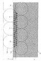
発光素子アレイのような光学系を用いる場合に、ラインヘッドの結像光学系としては、図14の説明図に示すような2列のロッドレンズを有するロッドレンズアレイを用いた等倍光学系が一般的に用いられる。図14において、84、84は2列に配置されたロッドレンズである。このロッドレンズアレイでは、主走査方向と平行なロッドレンズアレイの中心線と発光素子の位置を副走査方向において一致させる必要があるが、この位置がずれる場合がある。 When an optical system such as a light emitting element array is used, the line head imaging optical system is a 1 × optical system using a rod lens array having two rows of rod lenses as shown in FIG. Generally used. In FIG. 14, 84 and 84 are rod lenses arranged in two rows. In this rod lens array, the center line of the rod lens array parallel to the main scanning direction needs to coincide with the position of the light emitting element in the sub scanning direction, but this position may be shifted.
図14において、C.Lはロッドレンズアレイの中心線、Aは発光素子の位置がこの中心線C.Lから0.1mmずれた例、Bは発光素子の位置がこの中心線C.Lから0.2mmずれた例を示している。このように、発光素子の位置がロッドレンズアレイの中心線からずれる場合には、光量バラツキが生じる。図15(a)は主走査方向の光量バラツキを示す特性図、図15(b)は、副走査方向の光量分布データを示す特性図である。図15(b)に示すように、副走査方向に発光素子の位置がずれた場合の光量ばらつきは、ずれ量の正負対称に生じる。 In FIG. L is the center line of the rod lens array, and A is the position of the light emitting element. An example in which the position of the light emitting element is shifted from the center line C.I. An example of deviation from L by 0.2 mm is shown. As described above, when the position of the light emitting element is deviated from the center line of the rod lens array, the light amount varies. FIG. 15A is a characteristic diagram showing the light amount variation in the main scanning direction, and FIG. 15B is a characteristic diagram showing the light amount distribution data in the sub-scanning direction. As shown in FIG. 15B, the variation in the amount of light when the position of the light emitting element is shifted in the sub-scanning direction occurs in a symmetrical manner with respect to the shift amount.
図14の例では、ロッドレンズの直径を0.56mmとする。このときの図15(a)における主走査方向の光量バラツキは、発光素子の位置とロッドレンズアレイの中心線とのずれが0であれば、特性Daのように光量むら周期がロッドレンズの直径の1/2の0.28である。前記両者のずれ量が0.1mmのときには、光量むら周期はロッドレンズの直径の1/2の0.28mmと直径の0.56mmの和となる。この際の光量むら周期は、ずれ量が0の場合の2倍となる。前記両者のずれ量が0.2mmのときには、光量むら周期はロッドレンズの直径0.56mmとなる。 In the example of FIG. 14, the diameter of the rod lens is 0.56 mm. In this case, when the deviation between the position of the light emitting element and the center line of the rod lens array is 0, the unevenness of the light amount is the diameter of the rod lens. It is 0.28 of 1/2. When the amount of deviation between the two is 0.1 mm, the light amount unevenness period is a sum of 0.28 mm which is ½ of the diameter of the rod lens and 0.56 mm of the diameter. In this case, the light amount unevenness cycle is twice as long as the deviation amount is zero. When the amount of deviation between the two is 0.2 mm, the period of unevenness in the amount of light is 0.56 mm in diameter of the rod lens.
このように、発光素子の位置がロッドレンズアレイの中心線からずれる場合には、次のような問題が生じる。(1)ロッドレンズを通過する光量ムラの周期が2倍となり、光量ムラが認識しやすくなり画質の劣化が明瞭になる。(2)ロッドレンズを通過する光量の光量ムラが増加する。(3)ロッドレンズを通過する光量が低下する。(4)結像性能が劣化して、スポット径が大きくなったり、ばらついたりする。 As described above, when the position of the light emitting element deviates from the center line of the rod lens array, the following problem occurs. (1) The period of unevenness in the amount of light passing through the rod lens is doubled, making it easy to recognize the unevenness in the amount of light and making the deterioration of the image quality clear. (2) Unevenness in the amount of light passing through the rod lens increases. (3) The amount of light passing through the rod lens decreases. (4) The imaging performance deteriorates, and the spot diameter increases or varies.
従来の発光素子として特許文献1記載されているようなLEDを用いたラインヘッドでは、基板上に画像アレイを実装してラインヘッドを構成している。このため、実装誤差により発光部の画素列が直線にならず、全ての発光画素に対してレンズアレイの中心線を合わせる事が困難であった。さらに、発光部自身の光量ムラの方がレンズアレイの透過光量ムラよりも大きく、これを補正するためにヘッド通過後の光量に基づき発光素子1個1個に対して光量補正制御を行い、発光部自身の光量ムラとレンズアレイの透過光量ムラの両方を補正する必要があった。また、スポット径は補正することができないという問題があった。
In a line head using LEDs as described in
複数の発光素子で形成されるラインヘッドにおいては、このように、発光素子の中心とレンズの中心とを正確に位置合わせする事が問題となっているが、前記のように種々の問題があった。前記のように特許文献1に記載のLEDを用いたラインヘッドにおいては、発光素子アレイごとに中心検出位置、各レンズ毎に中心位置を示すためのマーキングを設ける方法が提案されている。
In a line head formed of a plurality of light emitting elements, as described above, there is a problem in accurately aligning the center of the light emitting element and the center of the lens. However, there are various problems as described above. It was. As described above, in a line head using LEDs described in
このようなマーキングを設ける方法においては、アレイの中心と基板の中心を検出し、これらの中心とレンズの中心が一致するように個々のレンズ位置の調整を行っていた。しかしながら、特許文献1に記載の方式では、複数のレンズがアレイ状になったレンズを使用する場合には、レンズ毎の調整を行う事ができないという問題があった。また、この方式では電極の形状によって中心位置を検出しているため、電極の形状が制約されるという問題があった。
In the method of providing such a marking, the center of the array and the center of the substrate are detected, and the individual lens positions are adjusted so that these centers coincide with the centers of the lenses. However, the method described in
本発明は従来技術のこのような問題点に鑑みてなされたものであり、その目的は、ロッドレンズの中心線と、発光素子ラインの中心との位置ずれを検出可能とし、透明基板の位置合わせを簡単な手段で行う光書込装置を提供することにある。 The present invention has been made in view of such problems of the prior art, its object is to the center line of the rod lens, and can detect the positional deviation of the center of the light-emitting element lines, the position of the transparent substrate An object of the present invention is to provide an optical writing apparatus that performs alignment by simple means.
上記目的を達成するために、本発明の光書込装置は、
主走査方向にライン状に配列した複数の発光素子と、
前記複数の発光素子の共通電極を形成した透明基板と、
前記発光素子に対向した位置に配置され、前記発光素子の出射光を被照射面に結像させるロッドレンズアレイと、を備え、
前記透明基板の主走査方向の長さを前記共通電極の長さよりも長く形成し、前記ロッドレンズアレイにおける中心線と、前記ライン状に配列した発光素子からなる発光素子ラインの中心線との位置合わせを行う調整手段を設けたことを特徴とする。
この構成によれば、透明基板の両側端部を透過する光で、検出手段によりロッドレンズアレイの中心線の位置を容易に検出することができるし、ロッドレンズアレイの中心線と、前記発光素子ラインの中心との位置ずれに起因する結像性能の低下を防止することができる。
In order to achieve the above object, an optical writing device of the present invention comprises:
A plurality of light emitting elements arranged in a line in the main scanning direction;
A transparent substrate on which a common electrode of the plurality of light emitting elements is formed;
A rod lens array that is disposed at a position facing the light emitting element and forms an image of light emitted from the light emitting element on an irradiated surface;
The length of the transparent substrate in the main scanning direction is longer than the length of the common electrode, and the position of the center line in the rod lens array and the center line of the light emitting element line composed of the light emitting elements arranged in the line shape An adjustment means for performing the alignment is provided.
According to this configuration, light transmitted through the two side portions of the transparent substrate, the position of the center line of the rod lens array to can be easily detected by the detecting means, and the center line of the rod lens array, the light emitting element It is possible to prevent a decrease in imaging performance due to a positional deviation from the center of the line.
また、本発明の光書込装置は、共通電極の副走査方向の幅を前記の透明基板の幅よりも狭く設定したことを特徴とする。この構成によれば、共通電極に遮断されることなく透明基板を透過する光量が増大するので、ロッドレンズアレイの中心線の検出が容易になるという利点がある。 Further, the optical writing device of the present invention is characterized in that the width of the common electrode in the sub-scanning direction is set narrower than the width of the transparent substrate . According to this configuration, the amount of light that passes through the transparent substrate without being blocked by the common electrode is increased, so that there is an advantage that the center line of the rod lens array can be easily detected.
また、本発明の光書込装置は、前記共通電極の副走査方向の幅を前記ロッドレンズアレイの幅と等しく設定したことを特徴とする。この構成によれば、共通電極の両側縁部を検出することにより、ロッドレンズアレイの幅も検出されることになり、ロッドレンズアレイの中心線の位置と発光素子ラインの中心との位置ずれの検出が簡単に行える。 In the optical writing device of the invention, the width of the common electrode in the sub-scanning direction is set equal to the width of the rod lens array. According to this configuration, the width of the rod lens array is also detected by detecting both side edges of the common electrode, and the positional deviation between the position of the center line of the rod lens array and the center of the light emitting element line is detected. Easy detection.
また、本発明の光書込装置は、前記共通電極の副走査方向の幅を前記ロッドレンズアレイの幅よりも狭く設定したことを特徴とする。この構成によれば、共通電極の両側の側縁と、各ロッドレンズアレイの外接線間の副走査方向の長さから、演算によりロッドレンズアレイの中心線の位置と発光素子ラインの中心との位置ずれの算出が可能となる。 In the optical writing device of the present invention, the width of the common electrode in the sub-scanning direction is set to be narrower than the width of the rod lens array. According to this configuration, from the side edges on both sides of the common electrode and the length in the sub-scanning direction between the circumscribing lines of each rod lens array, the position of the center line of the rod lens array and the center of the light emitting element line are calculated. The position deviation can be calculated.
また、本発明の光書込装置は、前記共通電極の副走査方向の幅を前記ロッドレンズアレイの幅よりも広く設定したことを特徴とする。この構成によれば、共通電極の一方側縁部を副走査方向の位置ずれ検出の基準としているので、ロッドレンズアレイの中心線と、発光素子ラインの中心との位置ずれを算出する処理が簡単に行える。 In the optical writing device of the present invention, the width of the common electrode in the sub-scanning direction is set wider than the width of the rod lens array. According to this configuration, since one side edge portion of the common electrode is used as a reference for detecting the displacement in the sub-scanning direction, the process of calculating the displacement between the center line of the rod lens array and the center of the light emitting element line is simple. Can be done.
また、本発明の光書込装置は、前記発光素子は有機EL素子であることを特徴とする。この構成によれば、工程上直線性を良好に製造できる有機EL素子を発光素子として用いているので、レンズアレイと発光部との位置ずれを精度良く検出することができる。 In the optical writing device of the present invention, the light emitting element is an organic EL element. According to this configuration, since the organic EL element that can be manufactured with good linearity in the process is used as the light emitting element, it is possible to accurately detect the positional deviation between the lens array and the light emitting unit.
また、本発明の光書込装置は、前記発光素子ラインは、副走査方向に複数列配列されていることを特徴とする。この構成によれば、光書込装置を多様な用途に適用することができる。 In the optical writing device of the present invention, the light emitting element lines are arranged in a plurality of columns in the sub-scanning direction. According to this configuration, the optical writing device can be applied to various uses.
本発明の光書込装置によれば、透明基板を有しているので、透明基板を通してロッドレンズアレイの位置確認を行う事ができる。このため、発光素子の共通電極幅をロッドレンズアレイの幅以下にする事によって、ロッドレンズの位置確認を容易に行う事ができる。したがって、簡単な手段で基板の位置調整が行え、結像性能を向上させ高画質な画像を得る構成とすることができる。
According to the optical writing apparatus of the present invention, since the transparent substrate is provided, the position of the rod lens array can be confirmed through the transparent substrate. For this reason, the position of the rod lens can be easily confirmed by setting the common electrode width of the light emitting elements to be equal to or smaller than the width of the rod lens array. Therefore, the position of the substrate can be adjusted by simple means, and the imaging performance can be improved to obtain a high-quality image.
以下、図を参照して本発明を説明する。図6は、光書込装置23を拡大して示す概略の斜視図である。図6においては、光書込装置23の細部が示されている。有機EL素子アレイ61は、長尺のハウジング60中に保持されている。長尺のハウジング60の両端に設けた位置決めピン69をケース50の対向する位置決め穴に嵌入させると共に、長尺のハウジング60の両端に設けたねじ挿入孔68を通して固定ねじをケース50のねじ穴にねじ込んで固定することにより、各像書込手段23が所定位置に固定される。
The present invention will be described below with reference to the drawings. FIG. 6 is a schematic perspective view showing the
光書込装置23は、ガラス基板(透明基板)62上に有機EL素子アレイ61の発光部63を載置し、同じガラス基板62上に形成されたTFT71により駆動される。屈折率分布型ロッドレンズアレイ65は結像光学系を構成し、発光部63の前面に配置される屈折率分布型ロッドレンズ84を俵積みしている。60はハウジング、66はカバー、67は固定板バネである。ハウジング60は、ガラス基板62の周囲を覆い、像担持体20に面した側は開放する。このようにして、屈折率分布型ロッドレンズ84から像担持体20に光線を射出する。したがって、屈折率分布型ロッドレンズ84は、発光素子の出射光を被照射面に結像させる手段として機能している。ハウジング60のガラス基板62の端面と対向する面には、光吸収性の部材(塗料)が設けられている。
In the
図7は、光書込装置23の副走査方向の断面図である。光書込装置23には、ハウジング60中の屈折率分布型ロッドレンズアレイ65の後面に面して取り付けられた有機EL素子アレイ61と、ハウジング60の背面から、その中の有機EL発光素子アレイ61を遮蔽する不透明なカバー66とが設けられている。また、固定板バネ67によりハウジング60の背面に対してカバー66を押圧して、ハウジング60内を光密に密閉する。すなわち、ガラス基板62は、固定板バネ67によりハウジング60で光学的に密閉されている。固定板バネ67は、ハウジング60の長手方向に複数個所設けられている。91は像担持体に形成される像面(被照射面)である。
FIG. 7 is a sectional view of the
ケースの内面に紫外線を吸収する黒色の塗料を塗布しておくと、有機EL素子アレイ61に対する紫外線遮蔽作用をより確実に行うことができ、有機EL発光素子の劣化を防止することができる。また、像書込手段23のハウジング60は不透明部材で形成され、その背面には不透明なカバー66により覆われている。このため、有機EL素子アレイ61の背面に入射する蛍光灯や太陽からの紫外線も、有機EL素子アレイ61の発光部63へ達することは防止される。83はガラス基板62をハウジング60に固定する接着剤である。
If a black paint that absorbs ultraviolet rays is applied to the inner surface of the case, the ultraviolet shielding effect on the organic
図8は、光書込装置23の主走査方向の断面図である。ガラス基板62は、有機EL素子を用いた発光部63をカバーガラス64で被覆している。このようなガラス基板62をハウジング60に固定する。この際に、ガラス基板62は、発光部63の位置とロッドレンズアレイ65の中心との位置決めがなされている。カバー66でガラス基板62を覆い板バネ67でカバー66を固定する。
FIG. 8 is a cross-sectional view of the
図9は、図7に示した有機EL発光素子アレイ61の発光部63近傍の構成例を示す断面図である。有機EL発光素子アレイ61は、例えば0.5mm厚のガラス基板62上に、各発光部63の発光を制御する厚さ50nmのポリシリコンからなるTFT(薄膜トランジスタ)71が、例えば千鳥配置の2列の発光部63各々に対応して欄外に設けられている。ガラス基板62上にはそのTFT71上のコンタクトホールを除いて厚さ100nm程度のSiO2からなる絶縁膜72が成膜され、コンタクトホールを介してTFT71に接続するように発光部63の位置に厚さ150nmのITOからなる陽極73が形成されている。
FIG. 9 is a cross-sectional view showing a configuration example in the vicinity of the
次いで、発光部63以外の位置に対応する部分には厚さ120nm程度のSiO2からなる別の絶縁膜74が成膜され、その上に発光部63に対応する穴76を形成した厚さ2μmのポリイミドからなる隔壁75が設けられる。その隔壁75の穴76内に、陽極73側から順に、厚さ50nmの正孔注入層77、厚さ50nmの発光層78が成膜され、その発光層78の上面と穴76の内面及び隔壁75の外面を覆うように、厚さ100nmのCuからなる陰極第1層79aと厚さ200nmのAlからなる陰極第2層79bとが順に成膜されている。
Then, another insulating
そして、その上に窒素ガス等の不活性ガス80を介して厚さ1mm程度のカバーガラス64でカバーされて、有機EL発光素子アレイ61の発光部63が構成されている。発光部63からの発光はガラス基板62側に行われる。なお、発光層78に用いる材料、正孔注入層77に用いる材料については、公知の種々のものが利用でき、詳細な説明は省略する。このような有機EL発光素子は、発光素子をガラス基板上に容易に作製することができるので、製造コストを低減することができる。
Then, the
図10は、光書込装置を位置決めする際の工程を示す説明図である。図10(a)で、ハウジング60の中央部に形成した開口部60aにロッドレンズアレイ65を挿入し、開口部60aに設けられている段差部60xでロッドレンズアレイ65の先端部を係止して、ハウジング60に固定する。(b)でガラス基板62に実装された発光部(図示を省略)をカバーガラス64で封止し、ガラス基板62をハウジング60内に挿入し、ハウジング60の内部に形成した段差部60yに載置する。
FIG. 10 is an explanatory diagram showing a process for positioning the optical writing device. In FIG. 10A, the
この状態でCCDカメラ90により、ガラス基板62上に実装されている発光部の位置と、ロッドレンズアレイ65の中心線C.Lとの位置ずれを検出し、後述する位置調整手段によりガラス基板62の位置決めを行う。この際、ガラス基板62は矢視X方向(副走査方向)に移動して位置決めを行う。前記位置決めが終了すると、(c)ガラス基板62を接着剤83でハウジング60に固定する。次に、(d)カバー66を取り付け、固定板バネ67でカバー66を押圧し、固定板バネ67の先端に形成した鉤部67aをハウジング60の外部に形成した段差部60zに係止して固定する。ハウジング60は、ロッドレンズアレイ65の保持手段として機能する。
In this state, the
図11は、位置ずれ検出の具体例を示す断面図である。図11は、図10(b)と対応している。図11において、ロッドレンズアレイ65はハウジング60に保持されており、ガラス基板62は位置ずれ調整後に接着剤83でハウジング60に固定される。ロッドレンズアレイの中心線をC.Lとするときに、ガラス基板62に形成された発光部63の中心の位置が、前記ロッドレンズアレイの中心線からΔLずれているものとする。この位置ずれは、CCDカメラ90により検出される。LaはCCDカメラ90の光路である。CCDカメラ90により検出された位置ずれ量は、図13に示されているメモリ103に記憶される。
FIG. 11 is a cross-sectional view illustrating a specific example of misregistration detection. FIG. 11 corresponds to FIG. In FIG. 11, the
図12は、本発明の光書込装置23の位置調整の例を示す平面図である。画像形成装置本体側のケースと固定するために、光書込装置23の基台89の両端には、ねじ挿入孔68a、68bが設けられている。図12の例では、屈折率分布型ロッドレンズ84は、副走査方向に2列に配列されている。
FIG. 12 is a plan view showing an example of position adjustment of the
基台89の中央部には、開口部89aが形成されており、ガラス基板62をこの開口部89aに挿入する。開口部89aの長手方向の一方側縁には、板バネ85a、85bが設けられている。ガラス基板62の長手方向の一方側縁を当該板バネ85a、85bで押圧する。そして、図10(b)で説明したCCDカメラ90で、ロッドレンズアレイの中心線を観察し、ガラス基板62を調整用ネジ86a、86bで調整しながら副走査方向に移動して、ロッドレンズアレイの中心線との位置決めを行う。
An
なお、この際に発光部63とロッドレンズアレイの中心線との位置ずれ量をCCDカメラ90で検出し、光量補正を行うためのデータを取得することができる。光量補正を行う場合には、図12のようなガラス基板62の位置調整は行わずに、図13のブロック図に示されているような制御手段により発光部の電圧または電流を制御して、電気的な手段により光量補正を行う。
At this time, the amount of positional deviation between the
このように、図12の実施形態例においては、工程上直線性を良好に製造できる有機EL素子を1ラインに複数配列して、発光部63とした光書込装置23に対して、ハウジングに対する取り付け誤差が少ないロッドレンズアレイの中心線を基準として位置ずれを検出する。このため、発光部63とロッドレンズアレイとの位置ずれを精度良く検出し、正確にガラス基板の位置合わせをすることができる。
As described above, in the embodiment shown in FIG. 12, a plurality of organic EL elements that can be manufactured with good linearity in the process are arranged in one line, and the
また、本発明の実施形態においては、ロッドレンズアレイとガラス基板、すなわち発光部との位置ずれ検出は、ガラス基板の後ろ側(有機EL素子の出力光の照射側とは反対側)から、ロッドレンズアレイを観察して行っている。このため、有機EL素子の出力光の影響を受けずに、ロッドレンズアレイとガラス基板の位置を観察できるので、両者間の位置ずれ検出を容易にかつ高精度に行うことができる。 Further, in the embodiment of the present invention, the detection of the positional deviation between the rod lens array and the glass substrate, that is, the light emitting unit is performed from the rear side of the glass substrate (the side opposite to the irradiation side of the output light of the organic EL element) from the rod. This is done by observing the lens array. For this reason, since the positions of the rod lens array and the glass substrate can be observed without being affected by the output light of the organic EL element, it is possible to easily detect the displacement between the two with high accuracy.
図13は、光書込装置の制御部の概略構成を示すブロック図である。図13において、101はラインヘッドの制御部、102は位置ずれ検出部、103はメモリ、104は制御回路、105はTFTからなる駆動回路である。106は発光素子が1ライン(主走査方向)に複数配列されている発光部である。
FIG. 13 is a block diagram illustrating a schematic configuration of a control unit of the optical writing device. In FIG. 13, 101 is a control unit of the line head, 102 is a misregistration detection unit, 103 is a memory, 104 is a control circuit, and 105 is a drive circuit comprising TFTs.
100は本体コントローラである。本体コントローラ100は、印刷データを形成してラインヘッドの制御部101に送信する。位置ずれ検出部102は、陰極とロッドレンズの中心線との位置ずれを検出する。メモリ103には、位置ずれ検出部102で検出された位置ずれ量を記憶させている。
制御回路104は、当該位置ずれ検出部102で検出された位置ずれ量の特性をメモリ103から読み出し、発光部106の中心とロッドレンズの中心線との位置ずれを算出する。また、制御回路104は、駆動回路104に信号を送出し、発光部106の印加電圧、または駆動電流を制御する。
The
図1は、本発明の実施形態を示す説明図である。図1において、ガラス基板62を通して図11で説明したCCDカメラ90により、ロッドレンズ84を観察する。複数の発光素子に対する共通電極としての陰極1(図9の図示番号79a、79bに対応する)の幅(副走査方向の長さ)Waは、ガラス基板62の幅Wbよりも狭く形成されている。このため、陰極1に遮断されることなくガラス基板(透明基板)62を透過する光量が増大するので、ロッドレンズアレイの中心線の検出が容易になるという利点がある。
FIG. 1 is an explanatory diagram showing an embodiment of the present invention. In FIG. 1, the
この際に、陰極1の両側の縁部もCCDカメラ90により検出されるので、制御部において、ロッドレンズアレイの中心線の位置と、図示を省略している発光素子ラインとの位置ずれを算出することができる。したがって、図12で説明した調整ねじ86a、86b、調整ばね85a、85bを用いて、ガラス基板62の副走査方向の位置を調整し、ロッドレンズアレイの中心線の位置と発光素子ラインの中心位置との位置合わせを行うことができる。
At this time, since the edge portions on both sides of the
図2は、本発明の他の実施形態を示す説明図である。図2において、陰極2の幅は、ガラス基板62の幅とほぼ等しく、一方側縁部2aはガラス基板62の側縁部と重ね合わせている。また、陰極2の主走査方向の長さは、ガラス基板62の長さよりも短くしている。この例では、ガラス基板62の両側端部を透過する光でCCDカメラ90によりロッドレンズアレイの中心線の位置を検出することができる。
FIG. 2 is an explanatory view showing another embodiment of the present invention. In FIG. 2, the width of the
また、陰極2もCCDカメラ90により検出される。図2の例においても、ロッドレンズアレイの中心線の位置と、発光素子ラインとの位置ずれを算出し、図12の機構を用いてロッドレンズアレイの中心線の位置と発光素子ラインの中心位置との位置合わせを行うことができる。
The
図3は、本発明の他の実施形態を示す説明図である。図3において、陰極3の幅は、ロッドレンズ84の幅と同じ寸法としている。図3の例では、CCDカメラ90により陰極3の両側縁部を検出することにより、ロッドレンズ84の幅も検出されることになる。この場合には、陰極3の幅寸法の1/2がロッドレンズアレイの中心線となるので、ロッドレンズアレイの中心線の位置と、発光素子ラインとの位置ずれを算出する処理が簡略化される。
FIG. 3 is an explanatory view showing another embodiment of the present invention. In FIG. 3, the width of the
図4は、本発明の他の実施形態を示す説明図である。図4において、陰極4の幅は、ロッドレンズ84a、84bの幅よりも狭くしている。ガラス基板62は、一部のみ表示している。10、11は、主走査方向に複数の発光部(発光素子)63を配列した発光素子ラインである。Y1は、陰極4の一方の側縁とロッドレンズ84aの外接線間の長さ、Y2は、陰極4の他方の側縁とロッドレンズ84bの外接線間の長さである。
FIG. 4 is an explanatory view showing another embodiment of the present invention. In FIG. 4, the width of the
CCDカメラ90により、Y1、Y2を検出することにより、ロッドレンズアレイの中心線CLと陰極4との位置ずれが検出できる。陰極4の両側縁部から、各発光素子ライン10、11の中心との長さは予め設定されており既知であるので、ロッドレンズアレイの中心線CLと、発光素子ライン10、11の中心との位置ずれを算出することができる。図4の構成は、発光素子ライン10、11を副走査方向に複数列配列しているので、光書込装置を多重露光のような多様な用途に適用することができる。なお、本発明の実施形態においては、発光素子ラインがガラス基板に1ライン形成される場合にも適用される。
By detecting Y1 and Y2 with the
図5は、本発明の他の実施形態を示す説明図である。図5において、陰極5の幅は、ロッドレンズ84の幅よりも広く形成している。Y3は、陰極5の一方の側縁部5aとロッドレンズ84bの外接線間の長さである。陰極5の一方の側縁部5aから、各発光素子ライン10、11の中心との長さは予め設定されており既知である。
FIG. 5 is an explanatory view showing another embodiment of the present invention. In FIG. 5, the width of the
図5の例では、Y3の長さ、すなわち、2ライン配列されているロッドレンズの中で、一方のロッドレンズ84bの外接線から陰極5の側縁部5a間の長さを検出することにより、発光素子ライン10、11の
位置ずれを検出することにある。このため、ロッドレンズアレイの中心線CLと各発光素子ライン10、11の中心との位置ずれが検出できる。図5の例では、陰極5の一方側縁部5aを副走査方向の位置ずれ検出の基準としているので、ロッドレンズアレイの中心線CLと、発光素子ライン1、2の中心との位置ずれを算出する処理が簡単に行える。
In the example of FIG. 5, by detecting the length of Y3, that is, the length between the side edges 5a of the
光書込装置の発光部に有機EL素子を用いた場合には、発光画素列は単一の基板上に半導体プロセスを用いて製造されるため、その直線性は、従来のLEDに比べて極めて高精度に構成することが可能となる。さらに、発光素子自身の光量ムラもレンズアレイの透過光量ムラに比べて小さく、レンズアレイの中心線と発光素子列を高精度に位置決めできれば、光量補正がなくとも光量を均一にすることができ、スポット径も均一となる。このため、高画質なラインヘッドを構成することができる。本発明は、このような有機EL素子の特性に着目して、光書込装置の位置ずれを検出すものである。 When an organic EL element is used for the light-emitting portion of the optical writing device, the light-emitting pixel column is manufactured on a single substrate using a semiconductor process, so its linearity is much higher than that of a conventional LED. It is possible to configure with high accuracy. Furthermore, the light amount unevenness of the light emitting element itself is also smaller than the transmitted light amount unevenness of the lens array, and if the center line of the lens array and the light emitting element row can be positioned with high accuracy, the light amount can be made uniform without light amount correction, The spot diameter is also uniform. For this reason, a high-quality line head can be configured. The present invention detects misalignment of an optical writing device by paying attention to the characteristics of such an organic EL element.
以上、本発明の光書込装置をいくつかの実施例に基づいて説明したが、本発明はこれら実施例に限定されず種々の変形が可能である。 The optical writing apparatus of the present invention has been described based on some embodiments. However, the present invention is not limited to these embodiments, and various modifications can be made.
1〜5・・・陰極(共通電極)、10、11・・・発光素子ライン、23・・・光書込装置、61・・・有機EL素子アレイ、62・・・ガラス基板(透明基板)、63・・・発光部、64・・・カバーガラス、65…屈折率分布型ロッドレンズアレイ(SLA)、84・・・屈折率分布型ロッドレンズ、85a、85b・・・板バネ、86a、86b・・・調整用ネジ、88・・・駆動回路、90・・・CCDカメラ、100・・・本体コントローラ、101・・・制御部、102・・・位置ずれ検出部、103・・・メモリ、104・・・制御回路、105・・・駆動回路、106・・・発光部。 DESCRIPTION OF SYMBOLS 1-5 ... Cathode (common electrode) 10, 11 ... Light emitting element line, 23 ... Optical writing apparatus, 61 ... Organic EL element array, 62 ... Glass substrate (transparent substrate) , 63 ... Light emitting part, 64 ... Cover glass, 65 ... Refractive index distribution type rod lens array (SLA), 84 ... Refractive index distribution type rod lens, 85a, 85b ... Leaf spring, 86a, 86b ... Adjustment screw, 88 ... Drive circuit, 90 ... CCD camera, 100 ... Main body controller, 101 ... Control unit, 102 ... Position detection unit, 103 ... Memory , 104... Control circuit, 105... Drive circuit, 106.
Claims (7)
前記複数の発光素子の共通電極を形成した透明基板と、
前記発光素子に対向した位置に配され、前記発光素子の出射光を被照射面に結像させるロッドレンズアレイと、を備え、
前記透明基板の主走査方向の長さを前記共通電極の長さよりも長く形成し、前記ロッドレンズアレイにおける中心線と前記ライン状に配した発光素子からなる中心線との位置合わせを行う調整手段を設けたことを特徴とする、光書込装置。
A plurality of light emitting elements arranged in a line in the main scanning direction;
A transparent substrate on which a common electrode of the plurality of light emitting elements is formed;
A rod lens array that is disposed at a position facing the light emitting element and forms an image of the emitted light of the light emitting element on an irradiated surface;
An adjusting means for forming the length of the transparent substrate in the main scanning direction longer than the length of the common electrode and aligning the center line of the rod lens array with the center line of the light emitting elements arranged in a line shape An optical writing device, comprising:
2. The optical writing device according to claim 1, wherein the width of the common electrode in the sub-scanning direction is set narrower than the width of the transparent substrate.
3. The optical writing device according to claim 1, wherein the width of the common electrode in the sub-scanning direction is set equal to the width of the rod lens array .
3. The optical writing device according to claim 1, wherein a width of the common electrode in the sub-scanning direction is set to be narrower than a width of the rod lens array .
3. The optical writing device according to claim 1, wherein a width of the common electrode in the sub-scanning direction is set wider than a width of the rod lens array .
The optical writing apparatus according to claim 1, wherein the light emitting element is an organic EL element.
Priority Applications (4)
| Application Number | Priority Date | Filing Date | Title |
|---|---|---|---|
| JP2004343604A JP4595511B2 (en) | 2004-11-29 | 2004-11-29 | Optical writing device |
| EP05025969A EP1661718A3 (en) | 2004-11-29 | 2005-11-29 | Optical writing device and method of manufacturing the same |
| US11/290,611 US7486306B2 (en) | 2004-11-29 | 2005-11-29 | Optical writing device and method of manufacturing the same |
| US12/275,022 US20090078854A1 (en) | 2004-11-29 | 2008-11-20 | Optical Writing Device and Method of Manufacturing the Same |
Applications Claiming Priority (1)
| Application Number | Priority Date | Filing Date | Title |
|---|---|---|---|
| JP2004343604A JP4595511B2 (en) | 2004-11-29 | 2004-11-29 | Optical writing device |
Publications (3)
| Publication Number | Publication Date |
|---|---|
| JP2006150714A JP2006150714A (en) | 2006-06-15 |
| JP2006150714A5 JP2006150714A5 (en) | 2008-01-17 |
| JP4595511B2 true JP4595511B2 (en) | 2010-12-08 |
Family
ID=36629576
Family Applications (1)
| Application Number | Title | Priority Date | Filing Date |
|---|---|---|---|
| JP2004343604A Expired - Fee Related JP4595511B2 (en) | 2004-11-29 | 2004-11-29 | Optical writing device |
Country Status (1)
| Country | Link |
|---|---|
| JP (1) | JP4595511B2 (en) |
Families Citing this family (1)
| Publication number | Priority date | Publication date | Assignee | Title |
|---|---|---|---|---|
| JP5531763B2 (en) * | 2010-05-07 | 2014-06-25 | 富士通株式会社 | Optical transmission device and optical transmission system |
Citations (4)
| Publication number | Priority date | Publication date | Assignee | Title |
|---|---|---|---|---|
| JPH07186444A (en) * | 1993-12-24 | 1995-07-25 | Kyocera Corp | Imaging device |
| JPH0952385A (en) * | 1995-08-14 | 1997-02-25 | Oki Data:Kk | Led head and method for adjusting position thereof |
| JPH09226172A (en) * | 1996-02-27 | 1997-09-02 | Oki Electric Ind Co Ltd | Organic el array printing head |
| JP2003341140A (en) * | 2002-05-31 | 2003-12-03 | Seiko Epson Corp | Optical head and imaging apparatus using the same |
-
2004
- 2004-11-29 JP JP2004343604A patent/JP4595511B2/en not_active Expired - Fee Related
Patent Citations (4)
| Publication number | Priority date | Publication date | Assignee | Title |
|---|---|---|---|---|
| JPH07186444A (en) * | 1993-12-24 | 1995-07-25 | Kyocera Corp | Imaging device |
| JPH0952385A (en) * | 1995-08-14 | 1997-02-25 | Oki Data:Kk | Led head and method for adjusting position thereof |
| JPH09226172A (en) * | 1996-02-27 | 1997-09-02 | Oki Electric Ind Co Ltd | Organic el array printing head |
| JP2003341140A (en) * | 2002-05-31 | 2003-12-03 | Seiko Epson Corp | Optical head and imaging apparatus using the same |
Also Published As
| Publication number | Publication date |
|---|---|
| JP2006150714A (en) | 2006-06-15 |
Similar Documents
| Publication | Publication Date | Title |
|---|---|---|
| US10776065B2 (en) | Display device comprising two display panels | |
| KR101198374B1 (en) | Light emitting diode substrate and manufacturing method thereof and liquid crystal display using the same | |
| CN112385057A (en) | Display panel, electronic apparatus including the same, and method of manufacturing display panel | |
| US7486306B2 (en) | Optical writing device and method of manufacturing the same | |
| US10566403B2 (en) | Display device, manufacturing method for display device, and electronic device with substrate spacer | |
| JP2001085160A (en) | Light emitting element with function of correcting light emission output | |
| KR20100011469A (en) | Inkjet printing system and manufacturing method of display device using the same | |
| US7199769B2 (en) | Exposure apparatus | |
| US8493422B2 (en) | Color filter layer alignment | |
| JP4649963B2 (en) | Optical writing device | |
| JP4595511B2 (en) | Optical writing device | |
| US11877500B2 (en) | Mask assembly | |
| CN103072385B (en) | Optical printing head and imaging device | |
| US20070046765A1 (en) | Image forming apparatus | |
| JP4552629B2 (en) | Optical writing apparatus and position adjustment method thereof | |
| JP2008146956A (en) | Light-emitting device, electronic apparatus, and detecting method of carrier balancing | |
| JP2006082451A (en) | Position adjusting method of line head and position adjuster | |
| JP3853318B2 (en) | Optical printer head | |
| JP2006130663A (en) | Optical line head | |
| KR100786177B1 (en) | Liquid crystal display device | |
| JP2006082450A (en) | Position adjusting method of line head and its position adjuster | |
| JP2006159455A (en) | Optical writing device | |
| JP2000025270A (en) | Optical printer head | |
| US20190146372A1 (en) | Optical writing device and image forming apparatus | |
| JPH1148532A (en) | Image-forming optical system, and printer head and image-forming apparatus using the same |
Legal Events
| Date | Code | Title | Description |
|---|---|---|---|
| A521 | Request for written amendment filed |
Free format text: JAPANESE INTERMEDIATE CODE: A523 Effective date: 20071126 |
|
| A621 | Written request for application examination |
Free format text: JAPANESE INTERMEDIATE CODE: A621 Effective date: 20071126 |
|
| A977 | Report on retrieval |
Free format text: JAPANESE INTERMEDIATE CODE: A971007 Effective date: 20100113 |
|
| A131 | Notification of reasons for refusal |
Free format text: JAPANESE INTERMEDIATE CODE: A131 Effective date: 20100217 |
|
| A521 | Request for written amendment filed |
Free format text: JAPANESE INTERMEDIATE CODE: A821 Effective date: 20100302 |
|
| RD04 | Notification of resignation of power of attorney |
Free format text: JAPANESE INTERMEDIATE CODE: A7424 Effective date: 20100302 |
|
| A521 | Request for written amendment filed |
Free format text: JAPANESE INTERMEDIATE CODE: A523 Effective date: 20100415 |
|
| RD03 | Notification of appointment of power of attorney |
Free format text: JAPANESE INTERMEDIATE CODE: A7423 Effective date: 20100415 |
|
| A131 | Notification of reasons for refusal |
Free format text: JAPANESE INTERMEDIATE CODE: A131 Effective date: 20100622 |
|
| A521 | Request for written amendment filed |
Free format text: JAPANESE INTERMEDIATE CODE: A523 Effective date: 20100630 |
|
| TRDD | Decision of grant or rejection written | ||
| A01 | Written decision to grant a patent or to grant a registration (utility model) |
Free format text: JAPANESE INTERMEDIATE CODE: A01 Effective date: 20100824 |
|
| A01 | Written decision to grant a patent or to grant a registration (utility model) |
Free format text: JAPANESE INTERMEDIATE CODE: A01 |
|
| A61 | First payment of annual fees (during grant procedure) |
Free format text: JAPANESE INTERMEDIATE CODE: A61 Effective date: 20100906 |
|
| R150 | Certificate of patent or registration of utility model |
Free format text: JAPANESE INTERMEDIATE CODE: R150 |
|
| FPAY | Renewal fee payment (event date is renewal date of database) |
Free format text: PAYMENT UNTIL: 20131001 Year of fee payment: 3 |
|
| LAPS | Cancellation because of no payment of annual fees |