JP4588885B2 - Plasma processing system, plasma processing method, and gas injector - Google Patents
Plasma processing system, plasma processing method, and gas injector Download PDFInfo
- Publication number
- JP4588885B2 JP4588885B2 JP2000592857A JP2000592857A JP4588885B2 JP 4588885 B2 JP4588885 B2 JP 4588885B2 JP 2000592857 A JP2000592857 A JP 2000592857A JP 2000592857 A JP2000592857 A JP 2000592857A JP 4588885 B2 JP4588885 B2 JP 4588885B2
- Authority
- JP
- Japan
- Prior art keywords
- gas
- gas injector
- substrate
- injector
- chamber
- Prior art date
- Legal status (The legal status is an assumption and is not a legal conclusion. Google has not performed a legal analysis and makes no representation as to the accuracy of the status listed.)
- Expired - Lifetime
Links
- 238000012545 processing Methods 0.000 title claims description 74
- 238000003672 processing method Methods 0.000 title 1
- 239000000758 substrate Substances 0.000 claims description 136
- 238000000034 method Methods 0.000 claims description 108
- 230000008569 process Effects 0.000 claims description 89
- 238000002347 injection Methods 0.000 claims description 44
- 239000007924 injection Substances 0.000 claims description 44
- 229910021420 polycrystalline silicon Inorganic materials 0.000 claims description 24
- 229920005591 polysilicon Polymers 0.000 claims description 24
- 239000000460 chlorine Substances 0.000 claims description 12
- 239000004065 semiconductor Substances 0.000 claims description 10
- VYPSYNLAJGMNEJ-UHFFFAOYSA-N Silicium dioxide Chemical compound O=[Si]=O VYPSYNLAJGMNEJ-UHFFFAOYSA-N 0.000 claims description 9
- 238000001020 plasma etching Methods 0.000 claims description 9
- 229910052801 chlorine Inorganic materials 0.000 claims description 8
- 230000001154 acute effect Effects 0.000 claims description 7
- 229910052782 aluminium Inorganic materials 0.000 claims description 7
- XAGFODPZIPBFFR-UHFFFAOYSA-N aluminium Chemical compound [Al] XAGFODPZIPBFFR-UHFFFAOYSA-N 0.000 claims description 7
- 238000005229 chemical vapour deposition Methods 0.000 claims description 6
- ZAMOUSCENKQFHK-UHFFFAOYSA-N Chlorine atom Chemical compound [Cl] ZAMOUSCENKQFHK-UHFFFAOYSA-N 0.000 claims description 4
- 229910052731 fluorine Inorganic materials 0.000 claims description 4
- 229910052794 bromium Inorganic materials 0.000 claims description 3
- 239000003989 dielectric material Substances 0.000 claims description 3
- 239000011737 fluorine Substances 0.000 claims description 3
- WKBOTKDWSSQWDR-UHFFFAOYSA-N Bromine atom Chemical compound [Br] WKBOTKDWSSQWDR-UHFFFAOYSA-N 0.000 claims 2
- YCKRFDGAMUMZLT-UHFFFAOYSA-N Fluorine atom Chemical compound [F] YCKRFDGAMUMZLT-UHFFFAOYSA-N 0.000 claims 2
- GDTBXPJZTBHREO-UHFFFAOYSA-N bromine Substances BrBr GDTBXPJZTBHREO-UHFFFAOYSA-N 0.000 claims 2
- 229910052814 silicon oxide Inorganic materials 0.000 claims 2
- 238000007789 sealing Methods 0.000 claims 1
- 239000007789 gas Substances 0.000 description 276
- 235000012431 wafers Nutrition 0.000 description 33
- 238000000151 deposition Methods 0.000 description 16
- 230000008021 deposition Effects 0.000 description 16
- 238000005530 etching Methods 0.000 description 14
- 238000009616 inductively coupled plasma Methods 0.000 description 12
- 230000005684 electric field Effects 0.000 description 9
- 150000002500 ions Chemical class 0.000 description 9
- 238000013461 design Methods 0.000 description 8
- 230000000694 effects Effects 0.000 description 8
- 239000000376 reactant Substances 0.000 description 7
- 239000006185 dispersion Substances 0.000 description 6
- 239000000463 material Substances 0.000 description 6
- 239000006227 byproduct Substances 0.000 description 5
- 238000009826 distribution Methods 0.000 description 5
- 238000005268 plasma chemical vapour deposition Methods 0.000 description 5
- XUIMIQQOPSSXEZ-UHFFFAOYSA-N Silicon Chemical compound [Si] XUIMIQQOPSSXEZ-UHFFFAOYSA-N 0.000 description 4
- 238000009792 diffusion process Methods 0.000 description 4
- 230000002093 peripheral effect Effects 0.000 description 4
- 235000012239 silicon dioxide Nutrition 0.000 description 4
- 230000015572 biosynthetic process Effects 0.000 description 3
- 125000001309 chloro group Chemical group Cl* 0.000 description 3
- 230000004907 flux Effects 0.000 description 3
- 229910052751 metal Inorganic materials 0.000 description 3
- 239000002184 metal Substances 0.000 description 3
- 238000001878 scanning electron micrograph Methods 0.000 description 3
- 229910052710 silicon Inorganic materials 0.000 description 3
- 239000010703 silicon Substances 0.000 description 3
- 239000000377 silicon dioxide Substances 0.000 description 3
- 239000000126 substance Substances 0.000 description 3
- 125000003821 2-(trimethylsilyl)ethoxymethyl group Chemical group [H]C([H])([H])[Si](C([H])([H])[H])(C([H])([H])[H])C([H])([H])C(OC([H])([H])[*])([H])[H] 0.000 description 2
- IJGRMHOSHXDMSA-UHFFFAOYSA-N Atomic nitrogen Chemical compound N#N IJGRMHOSHXDMSA-UHFFFAOYSA-N 0.000 description 2
- 230000002411 adverse Effects 0.000 description 2
- 238000013459 approach Methods 0.000 description 2
- 238000011109 contamination Methods 0.000 description 2
- 238000001816 cooling Methods 0.000 description 2
- 230000008878 coupling Effects 0.000 description 2
- 238000010168 coupling process Methods 0.000 description 2
- 238000005859 coupling reaction Methods 0.000 description 2
- 238000000354 decomposition reaction Methods 0.000 description 2
- 238000010586 diagram Methods 0.000 description 2
- 238000010494 dissociation reaction Methods 0.000 description 2
- 230000005593 dissociations Effects 0.000 description 2
- 239000010408 film Substances 0.000 description 2
- 229910052736 halogen Inorganic materials 0.000 description 2
- 150000002367 halogens Chemical class 0.000 description 2
- 238000007654 immersion Methods 0.000 description 2
- 238000002513 implantation Methods 0.000 description 2
- 239000011261 inert gas Substances 0.000 description 2
- 229920002120 photoresistant polymer Polymers 0.000 description 2
- 229920000642 polymer Polymers 0.000 description 2
- -1 quartz Chemical compound 0.000 description 2
- 238000004626 scanning electron microscopy Methods 0.000 description 2
- 239000007921 spray Substances 0.000 description 2
- 238000009827 uniform distribution Methods 0.000 description 2
- BSYNRYMUTXBXSQ-UHFFFAOYSA-N Aspirin Chemical compound CC(=O)OC1=CC=CC=C1C(O)=O BSYNRYMUTXBXSQ-UHFFFAOYSA-N 0.000 description 1
- PXGOKWXKJXAPGV-UHFFFAOYSA-N Fluorine Chemical compound FF PXGOKWXKJXAPGV-UHFFFAOYSA-N 0.000 description 1
- 230000003213 activating effect Effects 0.000 description 1
- PNEYBMLMFCGWSK-UHFFFAOYSA-N aluminium oxide Inorganic materials [O-2].[O-2].[O-2].[Al+3].[Al+3] PNEYBMLMFCGWSK-UHFFFAOYSA-N 0.000 description 1
- 229910021417 amorphous silicon Inorganic materials 0.000 description 1
- QVGXLLKOCUKJST-UHFFFAOYSA-N atomic oxygen Chemical compound [O] QVGXLLKOCUKJST-UHFFFAOYSA-N 0.000 description 1
- 230000008901 benefit Effects 0.000 description 1
- 239000012159 carrier gas Substances 0.000 description 1
- 238000005266 casting Methods 0.000 description 1
- 239000000919 ceramic Substances 0.000 description 1
- 230000008859 change Effects 0.000 description 1
- 238000006243 chemical reaction Methods 0.000 description 1
- 239000007806 chemical reaction intermediate Substances 0.000 description 1
- 239000011248 coating agent Substances 0.000 description 1
- 238000000576 coating method Methods 0.000 description 1
- 238000005260 corrosion Methods 0.000 description 1
- 230000007797 corrosion Effects 0.000 description 1
- 230000001627 detrimental effect Effects 0.000 description 1
- 230000009977 dual effect Effects 0.000 description 1
- 230000005520 electrodynamics Effects 0.000 description 1
- 238000005516 engineering process Methods 0.000 description 1
- 239000002360 explosive Substances 0.000 description 1
- 150000008282 halocarbons Chemical class 0.000 description 1
- 238000010438 heat treatment Methods 0.000 description 1
- 239000001257 hydrogen Substances 0.000 description 1
- 229910052739 hydrogen Inorganic materials 0.000 description 1
- 150000002431 hydrogen Chemical class 0.000 description 1
- 239000007943 implant Substances 0.000 description 1
- 239000000543 intermediate Substances 0.000 description 1
- 230000007246 mechanism Effects 0.000 description 1
- 150000002739 metals Chemical class 0.000 description 1
- 239000000203 mixture Substances 0.000 description 1
- 238000012986 modification Methods 0.000 description 1
- 230000004048 modification Effects 0.000 description 1
- 150000004767 nitrides Chemical class 0.000 description 1
- 229910052757 nitrogen Inorganic materials 0.000 description 1
- 238000009828 non-uniform distribution Methods 0.000 description 1
- 238000005457 optimization Methods 0.000 description 1
- 239000001301 oxygen Substances 0.000 description 1
- 229910052760 oxygen Inorganic materials 0.000 description 1
- 230000000149 penetrating effect Effects 0.000 description 1
- 230000008092 positive effect Effects 0.000 description 1
- 239000000843 powder Substances 0.000 description 1
- 239000010453 quartz Substances 0.000 description 1
- 239000012048 reactive intermediate Substances 0.000 description 1
- 238000011160 research Methods 0.000 description 1
- 238000005245 sintering Methods 0.000 description 1
- 229910001220 stainless steel Inorganic materials 0.000 description 1
- 239000010935 stainless steel Substances 0.000 description 1
- 239000010409 thin film Substances 0.000 description 1
- 238000000427 thin-film deposition Methods 0.000 description 1
Images


Classifications
-
- H01L21/205—
-
- H—ELECTRICITY
- H01—ELECTRIC ELEMENTS
- H01J—ELECTRIC DISCHARGE TUBES OR DISCHARGE LAMPS
- H01J37/00—Discharge tubes with provision for introducing objects or material to be exposed to the discharge, e.g. for the purpose of examination or processing thereof
- H01J37/32—Gas-filled discharge tubes
- H01J37/32431—Constructional details of the reactor
- H01J37/3244—Gas supply means
Landscapes
- Physics & Mathematics (AREA)
- Engineering & Computer Science (AREA)
- Plasma & Fusion (AREA)
- Chemical & Material Sciences (AREA)
- Analytical Chemistry (AREA)
- Drying Of Semiconductors (AREA)
- Physical Or Chemical Processes And Apparatus (AREA)
- Chemical Vapour Deposition (AREA)
Description
【0001】
(発明の分野)
本発明は、半導体ウェハなど半導体基板用のプラズマ処理システム内で基板に反応物を噴出するためのシステムおよび方法に関する。より詳細には、本発明は、処理均一性および効率を最大限にするためにガス注入システムを介して反応物を噴出するためのシステムおよび方法に関する。
【0002】
(発明の背景)
一般に、真空処理チャンバを使用して、真空チャンバにプロセス・ガスを供給し、ガスに高周波数(RF)場を印加することによって、基板上の材料のエッチングまたは化学気相成長(CVD)が行われる。基板にわたる一様な分散を保証するために、シャワーヘッド・ガス注入および拡散輸送システムが一般に使用されている。
【0003】
Roppel他に付与された米国特許第4691662号が、処理チャンバの側壁に取り付けられ、基板の一部を覆って延在する管路によってプロセス・ガスが供給されるエッチングおよび付着用のデュアル・プラズマ・マイクロ波装置を開示している。Suzuki他に付与された米国特許第5522934号は、基板に略垂直な方向で複数のレベルに位置決めされた複数のガス供給ノズルを含むガス注入器構成を開示している。上側レベルにあるガス供給ノズルは、下側レベルにあるノズルよりも基板の中心に向かってさらに延在している。ガス供給ノズルの遠位端部に注入穴が位置付けられている。これらのシステムは、基板上方の領域にプロセス・ガスを噴出するのに効果的である。しかし、基板と主イオン発生領域との間で基板表面を覆って管路が延在するため、発生領域から基板に向かってイオンが拡散するとき、管路が、基板表面上にイオン不均一な影を落とす可能性がある。これは、エッチおよび付着均一性の望ましくない損失をもたらす可能性がある。
【0004】
他の手法は、基板表面を覆って延在しないガス供給管路を採用する。J.Asmussenによる「Electron Cyclotron Resonance Microwave Discharges for Etching and Thin−film Deposition」,J.Vacuum Science and Technology A,Vol.7,pp.883−893(1989)は、基板端部までしか延在しない管路を示す。T.V.Herak等による「Low−temperature Deposition of Silicon Dioxide Films from Electron Cyclotron Resonant Microwave Plasmas」,J.Applied Physics,Vol.65,pp.2457−2463(1989)は、個別プロセス・ガスを供給する複数のガス注入管路を含むプラズマCVDツールを例示する。1組の管路が下側チャンバ壁内に取り付けられ、ガス噴出オリフィスが、基板支持体の周縁部のすぐ外側、および管路の遠位端部に位置付けられている。これらの管路構成は、管路の端部の加熱によるプロセス・ドリフト問題を生じる可能性がある。
【0005】
T.T.Chau等による「New Approach to Low Temperature Deposition of High−quality Thin Filmes by Electron Cyclotron Resonance Microwave Plasmas」,J.Vac.Sci.Tech,B,Vol.10,pp.2170−2178(1992)は、下側チャンバ壁内に取り付けられ、基板支持体の周縁部のすぐ上方および外側に位置付けられたガス入口管路を含むプラズマCVDツールを例示する。管路は曲がっており、それにより注入軸は基板に略平行である。追加の水平方向管路が第2のプロセス・ガス用に提供される。ガス注入オリフィスが、管路の遠位端部に位置付けられている。注入器チューブの遠位端部に位置付けられたオリフィスを有する注入器は、比較的少数の基板、例えば100枚の基板を処理した後に詰まってしまう傾向を有する場合がある。この注入器オリフィスの詰まりは、反応物の不均一な分散、不均一な被膜付着または基板のエッチング、および付着またはエッチ・レート全体のシフトをもたらす可能性があるため有害である。
【0006】
音速または超音速でプロセス・ガスを注入することによってプロセス均一性を改善するために、様々なシステムが提案されている。例えば、Hassan他に付与された米国特許第4270999号は、プラズマ・エッチおよび付着適用例のためのプロセス・ガスを音速で注入する利点を開示している。Hassan他は、ノズル中での音速の達成がノズルの真空末端からの爆発的放出を促進し、基板を取り囲む反応区域内でガス分子の高い渦巻き均一放散を生じることを述べている。Fiarbairn他に付与された米国特許第5614055号は、基板を覆う領域に向けて超音速で反応物ガスを噴霧する細長い超音速噴霧ノズルを開示する。ノズルは、チャンバ壁から基板に向かって延在し、各ノズル先端が、遠位端部にガス分散オリフィスを有する。Asmussen他に付与された米国特許第4943345号は、活性ガスを基板に向けるための超音速ノズルを含むプラズマCVD装置を開示する。Eres他に付与された米国特許第5164040号は、CVD用のパルス式超音速ジェットを開示する。これらのシステムはプロセス均一性を改善することを意図しているが、上述の欠点、すなわち注入器の遠位端部にあるオリフィスが詰まるという欠点があり、これが基板上の被膜均一性に悪影響を及ぼす可能性がある。
【0007】
Moslehi他に付与された米国特許第4996077号は、非プラズマ・ガスの均一分散を提供するために基板の周縁部の周りに配列されたガス注入器を含む電子サイクロトロン共鳴(ECR)デバイスを開示する。微粒子汚染を低減するために非プラズマ・ガスが注入され、注入器は、処理すべき基板表面上に非プラズマ・ガスを向けるように指向されている。
【0008】
Miyazaki他に付与された米国特許第5252133号は、長手方向軸に沿って複数のガス注入穴を有する垂直ガス供給チューブを含む複数ウェハ非プラズマCVD装置を開示する。注入穴は、複数の基板を支持するウェハ・ボートの長手方向側面に沿って延在して、チャンバ内にガスを導入する。同様に、Shishiguchi他に付与された米国特許第4992301号は、チューブの長さに沿ってガス放出穴を有する複数の垂直ガス供給チューブを開示する。これらの特許は、熱的非プラズマCVDに関係し、したがってプラズマ処理に最適なものではない。
【0009】
基板サイズが増大するにつれ、均一なエッチングおよび付着を保証するために中心ガス注入がますます重要になる。これは特にフラット・パネル表示処理では明白である。通常、これらの低圧処理システムでは基板上方の領域内で拡散輸送が優勢であり、対流輸送は役割がはるかに小さい。しかし注入オリフィス付近では、注入されるガスのジェット状性質のため、拡散輸送よりも対流輸送が優勢になる場合がある。したがって、基板により近接させて注入オリフィスを位置付けることにより、基板上方で、普通であれば優勢である拡散輸送に対して対流輸送が増大する。従来のシャワーヘッド・ガス注入システムは、基板の中心にガスを噴出することができ、しかし、基板に近接させてオリフィスを位置付けるためにはチャンバ高さを低減しなければならず、これは、イオン均一性の望ましくない損失をもたらす可能性がある。
【0010】
半径方向ガス注入システムは、例えばフラット・パネル処理で通常現れる大面積基板の中心への適切なプロセス・ガスの噴出を付与することができない。これは特に、プラズマ処理システムで一般に見られる底部ポンプ式チャンバ設計で当てはまる。中心ガス供給用の手段を有さないと、エッチ副生成物が基板中心の上方に沈滞する場合があり、これが、基板にわたる望ましくない不均一なエッチングおよびプロファイル制御をもたらす可能性がある。
【0011】
上述のFairbairn他の特許はまた、反応装置の天井に注入器オリフィスが位置付けられたシャワーヘッド注入システムを開示する。このシャワーヘッド・システムはさらに、複数の埋込磁石を含み、オリフィス詰まりを低減する。Tokuda他に付与された米国特許第5134965号は、処理チャンバの天井にある入口を介してプロセス・ガスが注入される処理システムを開示する。ガスは、高密度プラズマ領域に向けて供給される。このシステムは、マイクロ波エネルギーを採用しており、高周波プラズマ処理に最適ではない。Suzuki他に付与された米国特許第5522934号は、チャンバ天井の中心を介して不活性ガス(プロセス・ガスではない)が注入されるシステムを開示する。
【0012】
上述のシステムに加え、Hegedusに付与された米国特許第4614639号は、頂部壁にフレア状端部を有する中心ポートと、チャンバの周縁部の周りにある複数のポートとによってプロセス・ガスを供給される平行板反応装置を開示する。米国特許第5525159号(Hama他)、5529657号(Ishii)、5580385号(Paranjpe他)、5540800号(Qian)、および5531834号(Ishizuka他)は、シャワーヘッドによってプロセス・ガスを供給され、アンテナによってパワー供給され、チャンバ内に誘導結合プラズマを発生するプラズマ・チャンバ構成を開示する。
【0013】
したがって、基板の高周波プラズマ処理に関して均一性および付着を最適化し、その一方でガス供給オリフィスの詰まりおよび処理副生成物の堆積を防止し、かつウェハ上方での対流輸送を改善することが求められている。
【0014】
(発明の概要)
本発明は、プラズマ処理チャンバと、処理チャンバに接続された真空ポンプと、処理チャンバ内部で基板を支持する基板支持体と、基板支持体に面する内部表面を有する誘電体部材であって、処理チャンバの壁を形成する誘電体部材と、その遠位端部が処理チャンバ内部で露出されるように誘電体部材を介し、処理チャンバ内にプロセスガスを供給する複数のガス出口を含むガス注入器と、プロセスガスを励起してプラズマ状態にして基板を処理するために、誘電体部材を介してチャンバ内にRFエネルギーを誘導結合するRFエネルギー源とを含むプラズマ処理システムを提供する。システムは、好ましくは、高密度プラズマ化学気相成長システムまたは高密度プラズマエッチングシステムである。
【0015】
RFエネルギー源はRFアンテナを備えることができ、ガス注入器は、チャンバ内の主プラズマ発生区域に向けてプロセスガスを注入することができる。ガス出口を、ガス注入器の軸方向端面に位置付けることができる。例えば、ガス出口は、基板の露出面に垂直な軸方向に延在する中心ガス出口と、軸方向に対して鋭角で延在する複数の角度付きガス出口とを含むことができる。ガス注入器は、亜音速、音速、または超音速でプロセスガスを注入することができる。一実施形態では、ガス注入器が、誘電体窓の内部表面と同一平面にあるプレーナ形軸方向端面を含む。別の実施形態では、ガス注入器が、誘電体窓に着脱可能に取り付けられ、かつ/またはチャンバの中心領域内にプロセスガスを供給する。ガス出口は、様々な形状および/または空間配列を有することができる。例えば、ガス注入器は閉じた遠位端部を含むことができ、ガス出口は、基板の露出面に平行な平面に対して鋭角でプロセスガスを注入するように指向することができる。ガス注入器が誘電体窓にある開口内に着脱可能に取り付けられる場合、少なくとも1つのOリングが、ガス注入器と誘電体窓との間に真空シールを提供する。様々なタイプのプラズマ発生源を使用することができる。例えば、RFエネルギー源は、プレーナ形または非プレーナ形螺旋コイルの形でのRFアンテナを備えることができ、シャワーヘッドノズルが、チャンバ内の主プラズマ発生区域に向けてプロセスガスを注入する。
【0016】
本発明はまた、基板をプラズマ処理する方法であって、処理チャンバ内で基板支持体上に基板を配置することであって、処理チャンバの壁を形成する誘電体部材の内部表面が基板支持体に面していることと、遠位端部が処理チャンバ内部で露出されるように誘電体部材を介して延在するガス注入器から処理チャンバ内にプロセスガスを供給することであって、ガス注入器が、処理チャンバ内にプロセスガスを供給する複数のガス出口を含むことと、RFエネルギー源によって生成されたRFエネルギーを誘電体部材を介して処理チャンバ内に誘導結合することによってプロセスガスをプラズマ状態に励起することであって、プロセスガスが基板の露出面と反応するプラズマ相であることとを含む方法を提供する。
【0017】
(好ましい実施形態の詳細な説明)
本発明は、エッチングまたはCVDなどによって基板をプラズマ処理するための改良型ガス注入システムを提供する。この注入システムを使用して、珪素、ハロゲン(例えばF、Cl、Brなど)、酸素、水素、窒素などを含有するガスなど、ガスを注入することができる。この注入システムは単独で使用することができ、あるいは他の反応物/不活性ガス供給構成と共に使用することができる。
【0018】
本発明の1つの好ましい実施形態によれば、ガス注入構成が、誘導結合プラズマ・チャンバに提供される。好ましい構成では、ガス注入器がチャンバの上側壁の中心に位置付けられ、1つまたは複数のガス出口が、チャンバ内の処理すべき半導体基板の上方にプロセス・ガスを向ける。本発明によるガス注入器は、エッチ均一性、中心と縁部のプロファイル均一性、限界寸法(CD)バイアス、および/またはプロファイル・マイクロローディングを改善することができる。
【0019】
上側チャンバ壁の表面の下方、同一平面上、または上方にあるガス注入器の表面にガス出口を提供することができる。例えば、ガス注入器は、上側壁と半導体基板の露出面との間に位置付けられた、軸方向端部にガス出口を有する円筒形部材を備えることができる。本発明によれば、上側チャンバ壁の中心に位置付けられた単一ガス注入器を用いてエッチ結果の改善を達成することができる。ただし、特に誘電体層または窓によってチャンバの内部から離隔されたアンテナによってプラズマを発生する場合には、チャンバの上側壁に2つ以上のガス注入器を提供することができる。
【0020】
ガス出口の数および/またはガス出口から流出するガスの注入角度は、特定の基板処理体制(regime)で所望のガス分散を提供するように選択することができる。例えば、出口の数、サイズ、注入角度および/またはチャンバ内部での位置を、RFエネルギーをチャンバ内に誘導結合するために使用される特定のアンテナ設計、上側壁と基板の露出面との間のギャップ、および基板上で実施すべきエッチ・プロセスに適合させることができる。
【0021】
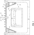
図1は、本出願の譲受人であるLAM Research Corporationによって製造されているTCP9100(登録商標)などのプラズマ・エッチ反応装置内の中心にガス注入器が取り付けられている本発明の一実施形態を示す。エッチ反応装置は、誘電体窓の外部に隣接して取り付けられているプレーナ形コイルなどのアンテナを含み、基板は、片持ち式静電チャックなどのチャックに支持されている。本発明によれば、プロセス・ガスをチャンバ内に供給するためにガス・リングまたはシャワーヘッドを使用する代わりに、ガス注入器が開口内に取り付けられ、誘電体窓を介して延在する。真空処理チャンバ10は、基板13に静電クランプ力を提供するとともに、上に支持された基板にRFバイアスを提供する基板ホルダ12と、基板をHe後方冷却しながら基板上方の領域内にプラズマを閉じ込めるための集束リング14とを含む。適切なRF源と、それに関連するRFインピーダンス整合回路19とによってパワー供給されるアンテナ18など、チャンバ内で高密度(例えば1011〜1012イオン/cm3)プラズマを維持するためのエネルギー源が、RFエネルギーをチャンバ10内に誘導結合し、それにより高密度プラズマを提供する。チャンバは、チャンバ内部を所望の圧力(例えば50mTorr未満、典型的には1〜20mTorr)で維持するための出口15に接続された適切な真空ポンプ装置を含む。均一な厚さの略プレーナ形誘電体窓20が、アンテナ18と処理チャンバ10内部との間に提供されて、処理チャンバ10の頂部に真空壁を形成する。ガス注入器22は、窓20にある開口内に提供され、ガス供給源23によって供給されるプロセス・ガスを処理チャンバ10に噴出するための円形穴(図示せず)など複数のガス出口を含む。円錐形ライナ30が窓20から延在し、基板ホルダ12を取り囲む。
【0022】
操作中、ウェハなどの半導体基板が基板ホルダ12上に位置決めされ、He後方冷却が採用されるときには通常、静電クランプ、機械的クランプ、またはその他のクランプ機構によって定位置に保持される。次いで、プロセス・ガスは、プロセス・ガスをガス注入器22に通すことによって真空処理チャンバ10に供給される。窓20は、図1に示されるようにプレーナ形であって均一な厚さを有していてよく、あるいは、非プレーナ形および/または不均一厚さ幾何形状など他の形状を有していてもよい。適切なRFパワーをアンテナ18に供給することによって、基板と窓の間の空間内に高密度プラズマが生成される。個々の基板のエッチングが完成すると、処理済み基板がチャンバから取り外され、別の基板がチャンバ内に搬送されて、その処理が行われる。
【0023】
ガス注入器22は、窓と同じ材料からなる、または異なる材料からなる個別部材を備えることができる。例えば、ガス注入器を、アルミニウムまたはステンレス鋼などの金属、または石英、アルミナ、珪素、窒化物などの誘電体材料から作成することができる。1つの好ましい実施形態によれば、ガス注入器が、窓にある開口内に着脱可能に取り付けられる。しかし、ガス注入器を窓と一体化することもできる。例えば、ガス注入器を、窓にある開口内にろう付けする、焼結する、またはその他の方法で結合することができ、あるいはガス注入器を、窓に機械加工する、またはその他の方法で形成することができる。例えば、ガス注入器を窓の形状に合わせて設計した状態で、Al2O3やSi3N4などセラミック粉末を焼結することによって窓を形成することができる。
【0024】
図2Aおよび2Bは、処理チャンバの底部にある出口に接続された真空ポンプ17を有する誘導結合プラズマ反応装置における異なるガス供給構成のガス分散効果を示す。図2Aでは、プラズマ反応装置が本発明によるガス注入器を含み、図2Bの構成はガス・リング構成を含む。図2Aの構成では、ガス注入器は、ガス注入器の下側端部が窓の内側表面と同一平面上になるように窓の開口内に取り付けられる。
【0025】
図3A〜Cは、本発明によるガス注入器の詳細図である。図3Aの断面図に示されるように、ガス注入器22は、上側端部にフランジ42を有する円筒形本体40と、上側軸方向端部を介して延在する中心ボア44と、ボアと下側軸方向端部の外部表面との間に延在する複数のガス出口46と、Oリング溝48、50とを含む。図3Bの斜視図に示されるように、ガス注入器の上側軸方向端部は、対向する側面に一対の平坦面54、56を含む。図3Cの軸方向断面図に示されるように、4つのガス出口46がボア44の下側端部に開いており、各ガス出口46が90°離隔されている。
【0026】
図4は、本発明による頂部ガス注入を提供するガス注入器に適合された300mmLAM TCP(登録商標)プラズマ反応装置からの局所SiClx放出を、側部ガス注入を提供するガス・リングに適合された同じ反応装置と比べたグラフである。反応装置は、反応装置圧力10mTorr、RFアンテナに対するパワー800ワット、ESC内の底部電極に対するパワー150ワット、100sccmのCl2および100sccmのArで操作された。グラフに示されるように、300mmウェハの露出面上方でのエッチ副生成物分散の強度は、頂部ガス注入を用いると実質的により均一になる。
【0027】
図5は、本発明による頂部ガス注入を提供するガス注入器に適合された300mmLAM TCP(登録商標)プラズマ反応装置からの塩素原子分散のグラフである。反応装置は、反応装置圧力10mTorr、RFアンテナに対するパワー800ワット、ESC内の底部電極に対するパワー150ワット、100sccmのCl2および100sccmのArで操作された。グラフに示されるように、ウェハの露出面上方での塩素原子分散の強度は、300mmウェハにわたって実質的に均一である。
【0028】
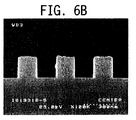
図6A〜Cは、ポリシリコン密集ラインでのエッチ・プロファイルのSEM(走査電子顕微鏡)イメージであり、図6D〜Fは、ポリシリコン孤立ラインでのエッチ・プロファイルのSEM(走査電子顕微鏡)イメージである。エッチ・プロファイルは、10mTorrで操作され、420sccmの総ガス流量を供給する頂部ガス注入器に適合された300mm反応装置内で処理される300mmウェハから得られる。図6Aは、ウェハの中心でのエッチ・プロファイルを示し、図6Bは、ウェハの中心と縁部の中間位置でのエッチ・プロファイルを示し、図6Cは、ウェハの縁部でのエッチ・プロファイルを示す。同様に、図6Dは、ウェハの中心でのエッチ・プロファイルを示し、図6Eは、ウェハの中心と縁部の中間位置でのエッチ・プロファイルを示し、図6Fは、ウェハの縁部でのエッチ・プロファイルを示す。これらのSEMイメージは、エッチ・プロファイルが300mmウェハにわたって実質的に均一であることを示す。
【0029】
図7A〜Dは、10mTorrの反応装置圧力で操作され、200sccmの総ガス流量を供給する頂部ガス注入器に適合された300mm反応装置で処理される300mmウェハにわたるポリシリコンのエッチ・プロファイルのSEM(走査電子顕微鏡)イメージである。図7Aは、ウェハの中心での密集ラインのエッチ・プロファイルを示し、図7Bは、ウェハの縁部での密集ラインのエッチ・プロファイルを示す。これらのSEMイメージは、エッチ・プロファイルが300mmウェハにわたって実質的に均一であることを示す。図7Cおよび7Dは、ウェハの中心および縁部での孤立ラインのエッチ・プロファイルを示す。デルタCD(ラインの上部と下部での幅の差)は、中心で68.75nm、縁部で56.25nmであり、中心と縁部でのデルタCDの差は12.5nm、すなわち0.0125μmである。
【0030】
図8A〜Dは、10mTorrの反応装置圧力で操作され、200sccmの総ガス流量を供給する側部ガス注入に適合された300mm反応装置で処理される300mmウェハにわたるポリシリコンのエッチ・プロファイルのSEM(走査電子顕微鏡)イメージである。図8Aは、ウェハの中心での密集ラインのエッチ・プロファイルを示し、図8Bは、ウェハの縁部での密集ラインのエッチ・プロファイルを示す。これらのSEMイメージは、図7A〜Dに示される頂部ガス注入の場合ほどエッチ・プロファイルが300mmウェハにわたって均一でないことを示す。図8Cおよび8Dは、ウェハの中心および縁部での孤立ラインのエッチ・プロファイルを示す。デルタCDは、中心で112.5nmであり、縁部で62.5nmであり、中心と縁部でのデルタCDの差は50nm、すなわち0.05μmである。
【0031】
1つの好ましい実施形態によれば、ガス注入器は、直径が1インチ(2.5cm)であり、一端に8個または9個のガス出口を有する円筒形部材である。9ガス出口構成は、ポリシリコン・エッチング・プロセスに有用であり、8ガス出口構成は、アルミニウム・エッチング・プロセスに有用である。9穴構成では、1つの穴がガス注入器の軸方向端部の中心に提供され、8つの穴が、45°離隔されて、軸方向端部の外側周縁部に隣接して位置付けられる。8穴構成では、中心穴が省略される。いずれの場合にも、8つの穴が軸方向に延在することができる、またはガス注入器を介して一部延在するボアの中心軸に対してある角度を有することができる。好ましい角度は10〜75°であり、より好ましくは10〜45°であり、注入器の軸方向端面が窓の内側表面と同一平面にあるとき、約30°が最も望ましい注入角度である。
【0032】
ガス注入器に関する最も好ましい取付構成は、着脱可能な取付構成である。例えば、ガス注入器を、窓にねじ留めすることができ、あるいは適切なクランプ構成によって窓にクランプすることができる。好ましい着脱可能取付構成は、ガス注入器が、窓とガス注入器との間にただ1つまたは複数のOリングを有して、窓に単に摺動可能に嵌合されているものである。例えば、Oリングを、ガス注入器の下側部分の周りにある溝内に提供して、ガス注入器と窓の開口との間にシールを提供することができる。別のOリングを、ガス注入器の上側部分にある溝内に提供して、ガス注入器と窓の外部表面との間にシールを提供することができる。
【0033】
ガス注入器は、利点として、操作者が、プラズマ・エッチ反応装置用のプロセス・ガス供給構成を反応装置内のガス分散が最適になるように変更することができるようになっている。例えばアルミニウムをプラズマ・エッチングするときは、エッチする基板にプロセス・ガスを直接向けずに、プロセス・ガスを分散してプラズマにすることが望ましい。ポリシリコンをプラズマ・エッチングするときは、プロセス・ガスを分散してプラズマにし、エッチする基板にプラズマ・ガスを直接向けることが望ましい。さらなる最適化は、窓の内側表面の下方に所望の距離だけ延在する、かつ/または特定のガス出口構成を含むガス注入器を選択することを含むことができる。すなわち、エッチング・プロセスに応じて、ガス出口の数、例えばガス注入器の軸方向端部での、かつ/またはその側面に沿ったガス出口の位置、およびガス出口の注入角度を選択して、最適なエッチング結果を提供することができる。例えば、注入角度は、より大きなサイズの基板に関してより大きくすることが好ましい。
【0034】
ガス注入器は、処理される基板に向かってガスが直接注入されないようにチャンバ内部にプロセス・ガスを注入することによって、アルミニウムをプラズマ・エッチするために使用することができる。1つの好ましい実施形態では、ガス注入器は、その軸方向端部に中心ガス出口を含まない。そうではなく、軸方向端部の周縁部の周りに位置付けられた4個または8個のガス出口を使用して、基板の露出面に垂直な方向に対して30〜60°の角度、好ましくは30〜45°でガスを注入する。一例として、プロセス・ガスには、100〜500sccmのCl2とBCl3、Cl2とN2、またはBCl3とCl2とN2の混合物が含まれる。
【0035】
ガス注入器はまた、処理される基板に向けてガスが直接注入されるようにチャンバ内部にプロセス・ガスを注入することによって、ポリシリコンをプラズマ・エッチするために使用することができる。1つの好ましい実施形態では、ガス注入器が、その軸方向端部に中心ガス出口を含み、軸方向端部の周縁部の周りに位置付けられた4個または8個のガス出口を使用して、基板の露出面に垂直な方向に対して10〜70°、好ましくは30〜60°の角度でガスを注入する。一例として、プロセス・ガスには、100〜500sccmのCl2とHBrの混合物、単独のCl2、または単独のHBrが含まれる。
【0036】
反応装置内にプラズマを発生するために螺旋コイルを使用する誘導結合プラズマ反応装置では、ガス注入器の最も好ましい位置はコイルの中心である。そのような位置は、コイルによって形成されるプラズマのトロイダル区域へのガス注入器の露出を避ける。したがって、ガス出口は、プラズマ誘導反応物分解が小さい低電界強度領域内に位置付けられている。すなわち、ガス注入器の遠位端部を取り囲む薄い(例えば<1mm)プラズマ・シースの存在の効果が小さい。このシースは、普通であれば、(プラズマと接地注入器チューブとの電位差によって生じる)電界線を非常に大きくし、エッチングまたは付着中に局所的に増大した付着をもたらし、最終的にはそのような領域内に位置付けられた出口を塞ぐ可能性がある。本発明によれば、ガス注入器は、増大した電界の及ばない位置に位置付けられ、それにより特に半導体ウェハなど個別基板の連続プラズマ処理中の詰まりやすさを低減する。
【0037】
半導体基板を処理する際、基板が処理チャンバ140内に挿入され、機械的または静電クランプによって基板支持体にクランプされる。プロセス・ガスを処理チャンバ内で励起して高密度プラズマにすることによって、基板が処理チャンバ内で処理される。エネルギー源は、チャンバ内で高密度(例えば109〜1012イオン/cm3、好ましくは1010〜1012イオン/cm3)プラズマを維持する。例えば、適切なRF源および適切なRFインピーダンス整合回路によってパワー供給されるプレーナ形複数巻き螺旋コイル、非プレーナ形複数巻きコイル、または別の形状を有するアンテナなどのアンテナ150が、RFエネルギーをチャンバ内に誘導結合して、高密度プラズマを発生する。ただし、プラズマを、ECR、平行板、ヘリコン、螺旋共振器などのタイプのプラズマ源など他のプラズマ源によって発生することもできる。チャンバは、所望の圧力(例えば5Torr未満、好ましくは1〜100mTorr)でチャンバの内部を維持するための適切な真空ポンプ装置を含むことができる。均一な厚さのプレーナ形誘電体窓155または非プレーナ形誘電体窓などの誘電体窓がアンテナ150と処理チャンバ140内部との間に提供され、処理チャンバ140の頂部に真空壁を形成する。
【0038】
プロセス・ガスをチャンバ内に供給するガス供給源が、上述のガス注入器を含む。プロセス・ガスには、反応性ガスと、Arなど任意選択の搬送ガスとが含まれる。ガス出口の小さなオリフィス・サイズおよび数により、ガス注入器とチャンバ内部との間に大きな圧力差が発生する場合がある。例えば、ガス注入器での圧力が>1Torrであり、チャンバ内部での圧力が約10mTorrであるとき、圧力差は約100:1である。これは、ガス出口でのチョークされた音速の流れをもたらす。望みであれば、ガス出口の内部オリフィスは、出口で超音速の流れを提供するように輪郭を取ることができる。
【0039】
音速でのプロセス・ガスの注入は、プラズマがガス出口に浸透するのを妨げる。ドープまたはアンドープ二酸化シリコンなどの材料の付着の場合、そのような設計が、SiH4などのガスのプラズマ誘導分解、およびそれに続くガス出口内部でのアモルファスシリコン残留物の形成を防止する。この実施形態によるプラズマ処理システムは、基板の上方にシリコン含有プロセス・ガスを集中させることによって、かつ基板の特定の領域上にプロセス・ガスを優先的に向けることによって、従来のガス分散システムに比べ、基板での高い付着レートおよび改善された均一性を提供する。
【0040】
プロセス・ガスを活性化することによって発生するプラズマは、高い電気ポテンシャル、すなわちプラズマ電位で浮動する導電性ガスである。プラズマ電位は主に、プラズマとRF駆動基板電極との容量結合によって決まる。典型的な条件下では、プラズマ電位は数百ボルトに達する場合がある。ガス注入器は通常、プラズマよりも低い電位(例えば金属製注入器では接地電位)に保たれる。ガス注入器がプラズマ区域内に延在する場合、薄いシースをガス注入器の「プラズマ浸漬」部分の周りに形成することができ、この場合、プラズマと接地されたガス注入器との電位差によって生じる電界線はシースに垂直になる。これらの電界は、(基板支持体によって加えられる)バイアス・パワーがプラズマ電位を、RFパワー供給された基板支持体との容量結合により数百ボルトの大きさで振動させることによって、非常に大きくなる場合がある。外部構造コーナおよび縁部が、鋭いか丸み付けされているかに関わらず電界を集束するように作用することは周知である(例えばJohn David Jackson,John Wiley & Sonsによる「Classical Electrodynamics」,New York,1975,2nd ed.参照)。プラズマ処理装置内部の高い電界を有する領域が、高いガス解離をもたらす。したがって、ガス注入器の任意の先端またはコーナが局所電界を集束する傾向をもつ可能性があり、それにより電界線が、そのような幾何形状の周りに集中して、ガス注入器のそのような部分での高い局所解離およびそれに続く付着をもたらす。時間が経過するにつれ、付着物がガス出口を塞ぐ可能性があり、それによりプロセス均一性に悪影響を及ぼす。本発明によれば、ガス出口と、好ましくはガス注入器全体とをプラズマ形成区域外部に位置付けることによって詰まりの問題を解決することができる。
【0041】
本発明によれば、ハロゲンおよびハロカーボン・ベースの化学物質を使用した基底材料に対するフォトレジスト・エッチ均一性および選択性を含めた、アルミニウムなどの金属、ポリシリコンなどの導電半導体材料、および二酸化シリコンなどの誘電体材料のエッチ均一性が改善される。対照的に、誘電体窓内または下方に組み込まれたシャワーヘッドを介する従来の注入は、基板にわたる不均一なエッチング、例えば「中心高速レジスト・エッチング」を生じる場合があり、それが、エッチされたフィーチャおよびプロファイル、ならびに基板中心と縁部でのフィーチャの相違に関する制御を弱いものにする可能性がある。さらに、TCP(登録商標)窓またはシャワーヘッドでのポリマー形成が、望ましくない微粒子フレーキングおよび汚染を基板上にもたらす可能性がある。シャワーヘッド構成に関連する他の問題には、窓を横切ってガスを噴出するためのサンドイッチ型構造を提供することに関連する追加のコスト、温度制御、シャワーヘッドのガス/プラズマ腐食の影響、シャワーヘッド・ガス出口内、またはシャワーヘッドと覆い窓との間のギャップ内でのプラズマの生成、プロセス反復性の欠如、プロセス・ドリフトなどが含まれる。対照的に、ガス注入リングを介する縁部注入は、「縁部高速エッチング」およびチャンバ壁へのポリマー付着をもたらす場合がある。フォトレジスト対酸化物選択比は通常、これらの場合には1〜4しかなく、5〜10が望ましい。本発明によるガス注入器は、レジスト・エッチ・レート(通常6%3σ)の均一性の改善を提供することができ、同時にレジスト対酸化物選択比は5、好ましくは10以上となる。したがって、本発明の好ましい注入設計は、原子塩素やフッ素などのエッチ種と、CF、CF2、CF3などの重合種との両方を含めた反応中間体および化学的ラジカルなはるかに均一なフラックスを基板表面に提供すると思われる。
【0042】
基板サイズが増大するにつれ、中心に供給されるガスの必要性が高まる。ガス・リング構成からガスを供給する注入システムは、フラット・パネル処理で通常現れる大面積基板の中心に適切なプロセス・ガス噴出を付与することができない。これは特に、プラズマ処理システムで一般に見られる底部ポンプ式チャンバ設計で当てはまる。プラズマ・エッチングの場合、本発明による中心ガス供給を有さないと、エッチ副生成物が基板中心の上方に沈滞し、この場合、輸送は実質的に拡散のみによるものとなる。これは、基板にわたる望ましくない不均一エッチングをもたらす場合がある。本発明によれば、プロセス・ガスは、基板の中心に面し、かつ基板に近接するプラズマ領域内部に注入される。例えば、ガス注入器のガス出口を、窓の内側表面の十分下方に位置付けることができ、それによりガス出口はプラズマ内部に浸漬される。ガス出口は、好ましくは、均一なエッチまたは付着レートを保証するためにイオンおよび自然種の適切な拡散が存在するように位置付けられる。したがって、ガス注入器を、TCP(登録商標)コイルによって誘導される方位角電界がゼロに落ちる領域に位置付けることができ、それによりプラズマ発生区域の摂動を最小限に抑える。さらに、チャンバ天井と基板との距離の約80%以下など、適切な距離だけガス注入器が浸漬されることが好ましい。これは、チャンバの上側領域からのイオン拡散が、ガス注入器のすぐ下に、より低いイオン密度で充填するのに十分な空間を有することを保証する。これにより、イオン・フラックス内のガス注入器の基板への「影」を最小限に抑えることができる。
【0043】
浸漬ガス注入器の使用が、中心ガス供給位置とチャンバ縦横比を独立して選択することを可能にする。これは、プロセス・ガスの効率の良い利用を容易にし、プラズマ均一性に対する外乱を最小限に抑えた状態で大面積基板の中心領域へのプロセス・ガス噴出を改善する。この構成はまた、基板に近接するガス出口の位置付けが、基板のすぐ上方にある領域内で拡散輸送に対して対流輸送を増大させるので、有利である。反応物の噴出を改善することに加え、ガス注入器は、基板領域の外へエッチ副生成物を効率良く輸送することを容易にし、これは、特にアルミニウム・エッチングなど化学的駆動適用例でエッチ均一性およびプロファイル制御に良い影響を及ぼすことができる。
【0044】
1つの例示実施形態によれば、注入オリフィスは十分小さく、ガス注入器の周りに形成されたプラズマ・シースがガス出口の存在によって大きな影響を受けない。ガス出口の総面積は、ガス注入器にあるボアの断面積よりも小さい場合も、大きい場合も、または同じ場合もある。ガス出口の総面積は、好ましくは、チャンバ内部で一様に分散するようにプロセス・ガスが各ガス出口から噴出されることを保証する。基板上方の様々な領域への注入を、様々なガス出口に関して同じまたは異なる直径を利用することによって調整することができる。
【0045】
ガス出口は、長さ全体に沿った均一な直径、あるいは円錐形にテーパ付けされたフレア表面、または半径方向に輪郭を取られた表面などの他の形状など、任意の所望の形状を有することができる。ガス出口は、基板に直接的に、基板に対して鋭角で、基板に平行に、上側プラズマ境界面に向けて後ろに(ノズルの長手方向軸に関して鈍角で)、またはそれらの組合せでというように、任意の方向にガスを注入するように指向することができる。大面積基板にわたる均一なエッチおよび付着レートを容易にするために基板表面上への化学的ラジカルおよび反応中間体種の均一フラックスを達成することが望ましい。望みであれば、追加のガス注入構成も、基板の周縁部付近で、または他のチャンバ壁から提供することができる。
【0046】
好ましくは、先端付近での局所磁界増大を低減するために、ガス注入器の末端端部に鋭いコーナが存在しない。ただし、そのような磁界の増大が有利である場合もある。
【0047】
以上、本発明の原理、好ましい実施形態、および動作モードを説明した。しかし、本発明は、論じた特定の実施形態に制限するものと解釈すべきでない。したがって、上述の実施形態は制限するものではなく例示するものと見なすべきであり、頭記の特許請求の範囲によって定義される本発明の範囲を逸脱することなく当業者がいくつかの変更を加えることができることを理解されたい。
【図面の簡単な説明】
【図1】 本発明によるプラズマ処理システムを示す図である。
【図2A】 誘導結合プラズマ反応装置内でのガス分散効果を示す図であって、本発明によるガス注入構成を使用した効果を示す図である。
【図2B】 誘導結合プラズマ反応装置内でのガス分散効果を示す図であって、従来のガス・リング構成を使用した効果を示す図である。
【図3A】 本発明によるガス注入器設計の詳細図であり、ガス注入器の断面図である。
【図3B】 本発明によるガス注入器設計の詳細図であり、ガス注入器の斜視図である。
【図3C】 本発明によるガス注入器設計の詳細図であり、ガス注入器の軸方向断面図である。
【図4】 本発明による頂部ガス注入を提供するガス注入器に適合された300mmLAM TCP(登録商標)プラズマ反応装置からの局所SiClx放出を、側部ガス注入を提供するガス・リングに適合された同じ反応装置と比べたグラフである。
【図5】 本発明による頂部ガス注入を提供するガス注入器に適合された300mmLAM TCP(登録商標)プラズマ反応装置からの塩素原子分散のグラフである。
【図6A】 ポリシリコン密集ラインでのエッチ・プロファイルのSEM(走査電子顕微鏡)イメージである。
【図6B】 ポリシリコン密集ラインでのエッチ・プロファイルのSEM(走査電子顕微鏡)イメージである。
【図6C】 ポリシリコン密集ラインでのエッチ・プロファイルのSEM(走査電子顕微鏡)イメージである。
【図6D】 ポリシリコン孤立ラインでのエッチ・プロファイルのSEM(走査電子顕微鏡)イメージである。
【図6E】 ポリシリコン孤立ラインでのエッチ・プロファイルのSEM(走査電子顕微鏡)イメージである。
【図6F】 ポリシリコン孤立ラインでのエッチ・プロファイルのSEM(走査電子顕微鏡)イメージである。
【図7A】 本発明による頂部ガス注入器に適合されて操作される反応装置内で処理される300mmウェハにわたるポリシリコン密集ラインおよび孤立ラインのエッチ・プロファイルのSEM(走査電子顕微鏡)イメージである。
【図7B】 本発明による頂部ガス注入器に適合されて操作される反応装置内で処理される300mmウェハにわたるポリシリコン密集ラインおよび孤立ラインのエッチ・プロファイルのSEM(走査電子顕微鏡)イメージである。
【図7C】 本発明による頂部ガス注入器に適合されて操作される反応装置内で処理される300mmウェハにわたるポリシリコン密集ラインおよび孤立ラインのエッチ・プロファイルのSEM(走査電子顕微鏡)イメージである。
【図7D】 本発明による頂部ガス注入器に適合されて操作される反応装置内で処理される300mmウェハにわたるポリシリコン密集ラインおよび孤立ラインのエッチ・プロファイルのSEM(走査電子顕微鏡)イメージである。
【図8A】 反応装置内で処理され、側部ガス注入に適合する300mmウェハにわたるポリシリコン密集ラインおよび孤立ラインでのエッチ・プロファイルのSEM(走査電子顕微鏡)イメージである。
【図8B】 反応装置内で処理され、側部ガス注入に適合する300mmウェハにわたるポリシリコン密集ラインおよび孤立ラインでのエッチ・プロファイルのSEM(走査電子顕微鏡)イメージである。
【図8C】 反応装置内で処理され、側部ガス注入に適合する300mmウェハにわたるポリシリコン密集ラインおよび孤立ラインでのエッチ・プロファイルのSEM(走査電子顕微鏡)イメージである。
【図8D】 反応装置内で処理され、側部ガス注入に適合する300mmウェハにわたるポリシリコン密集ラインおよび孤立ラインでのエッチ・プロファイルのSEM(走査電子顕微鏡)イメージである。[0001]
(Field of Invention)
The present invention relates to a system and method for jetting reactants to a substrate in a plasma processing system for a semiconductor substrate such as a semiconductor wafer. More particularly, the present invention relates to a system and method for injecting reactants through a gas injection system to maximize process uniformity and efficiency.
[0002]
(Background of the Invention)
In general, a vacuum processing chamber is used to supply a process gas to the vacuum chamber and apply a high frequency (RF) field to the gas to perform etching or chemical vapor deposition (CVD) of the material on the substrate. Is called. Showerhead gas injection and diffusion transport systems are commonly used to ensure uniform distribution across the substrate.
[0003]
U.S. Pat. No. 4,691,662 to Roppel et al. Is a dual plasma process for etching and deposition that is attached to the sidewalls of the processing chamber and supplied with process gas by a conduit that extends over a portion of the substrate. A microwave device is disclosed. U.S. Pat. No. 5,522,934 to Suzuki et al. Discloses a gas injector configuration that includes a plurality of gas supply nozzles positioned at a plurality of levels in a direction generally perpendicular to the substrate. The gas supply nozzle at the upper level extends further toward the center of the substrate than the nozzle at the lower level. An injection hole is located at the distal end of the gas supply nozzle. These systems are effective for injecting process gas into the region above the substrate. However, since the pipeline extends over the substrate surface between the substrate and the main ion generation region, when the ions diffuse from the generation region toward the substrate, the pipeline is non-uniform on the substrate surface. There is a possibility of casting a shadow. This can lead to undesirable loss of etch and deposition uniformity.
[0004]
Another approach employs a gas supply line that does not extend over the substrate surface. J. et al. “Electron Cyclotron Resonance Microwave Discharges for Etching and Thin-film Deposition” by Asmussen, J. Am. Vacuum Science and Technology A, Vol. 7, pp. 883-893 (1989) indicates a conduit that extends only to the edge of the substrate. T. T. V. “Low-temperature Deposition of Silicon Dioxide Film from Electron Cyclotron Resonant Microwave Plasma,” by Herak et al. Applied Physics, Vol. 65, pp. 2457-2463 (1989) exemplifies a plasma CVD tool that includes a plurality of gas injection lines that supply individual process gases. A set of conduits are mounted in the lower chamber wall, and gas ejection orifices are located just outside the periphery of the substrate support and at the distal end of the conduit. These conduit configurations can cause process drift problems due to heating of the ends of the conduit.
[0005]
T. T. T. T. “New Approach to Low Temperature Deposition of High-quality Thin Films by Electron Cyclotron Resonance Microwave Plasma” by Cau et al. Vac. Sci. Tech, B, Vol. 10, pp. 2170-2178 (1992) illustrates a plasma CVD tool that is mounted in the lower chamber wall and includes a gas inlet line positioned just above and outside the peripheral edge of the substrate support. The conduit is bent so that the injection axis is substantially parallel to the substrate. An additional horizontal line is provided for the second process gas. A gas injection orifice is positioned at the distal end of the conduit. An injector having an orifice positioned at the distal end of the injector tube may have a tendency to become clogged after processing a relatively small number of substrates, eg, 100 substrates. This clogging of the injector orifice is detrimental because it can result in non-uniform distribution of reactants, non-uniform film deposition or substrate etching, and shift in overall deposition or etch rate.
[0006]
Various systems have been proposed to improve process uniformity by injecting process gas at sonic or supersonic speeds. For example, U.S. Pat. No. 4,270,999 to Hassan et al. Discloses the advantage of implanting process gas at sonic speeds for plasma etch and deposition applications. Hassan et al. State that achieving a speed of sound in the nozzle facilitates explosive emission from the vacuum end of the nozzle, resulting in a high vortex uniformity dissipation of gas molecules within the reaction zone surrounding the substrate. U.S. Pat. No. 5,614,055 issued to Fearbairn et al. Discloses an elongated supersonic spray nozzle that sprays reactant gas at supersonic speeds toward the area covering the substrate. Nozzles extend from the chamber wall toward the substrate, and each nozzle tip has a gas distribution orifice at the distal end. U.S. Pat. No. 4,943,345 to Asmussen et al. Discloses a plasma CVD apparatus including a supersonic nozzle for directing an active gas toward a substrate. US Pat. No. 5,164,040 to Eres et al. Discloses a pulsed supersonic jet for CVD. These systems are intended to improve process uniformity, but have the disadvantages described above, i.e., clogging the orifice at the distal end of the injector, which adversely affects coating uniformity on the substrate. There is a possibility of effect.
[0007]
U.S. Pat. No. 4,996,077 to Moslehi et al. Discloses an electron cyclotron resonance (ECR) device that includes a gas injector arranged around the periphery of the substrate to provide uniform distribution of non-plasma gas. . A non-plasma gas is injected to reduce particulate contamination and the injector is directed to direct the non-plasma gas onto the substrate surface to be processed.
[0008]
US Pat. No. 5,252,133 to Miyazaki et al. Discloses a multi-wafer non-plasma CVD apparatus including a vertical gas supply tube having a plurality of gas injection holes along the longitudinal axis. The injection holes extend along the longitudinal sides of the wafer boat that supports the plurality of substrates to introduce gas into the chamber. Similarly, US Pat. No. 4,992,301 to Shishiguchi et al. Discloses a plurality of vertical gas supply tubes having gas discharge holes along the length of the tube. These patents relate to thermal non-plasma CVD and are therefore not optimal for plasma processing.
[0009]
As the substrate size increases, central gas injection becomes increasingly important to ensure uniform etching and deposition. This is especially evident in flat panel display processing. Typically, in these low pressure processing systems, diffusive transport predominates in the region above the substrate, and convective transport plays a much smaller role. However, near the injection orifice, convective transport may dominate over diffusive transport due to the jet nature of the injected gas. Thus, locating the injection orifice closer to the substrate increases convective transport over the substrate, which would otherwise be dominant. Conventional showerhead gas injection systems can eject gas to the center of the substrate, but the chamber height must be reduced to position the orifice close to the substrate, which This can result in an undesirable loss of uniformity.
[0010]
A radial gas injection system cannot provide proper process gas ejection to the center of a large area substrate typically encountered, for example, in flat panel processing. This is particularly true with bottom pumped chamber designs commonly found in plasma processing systems. Without a means for central gas supply, etch by-products may stagnate above the substrate center, which can result in undesirable non-uniform etching and profile control across the substrate.
[0011]
The aforementioned Fairbairn et al. Patent also discloses a showerhead injection system in which an injector orifice is positioned in the reactor ceiling. The showerhead system further includes a plurality of embedded magnets to reduce orifice clogging. U.S. Pat. No. 5,134,965 to Tokuda et al. Discloses a processing system in which process gas is injected through an inlet in the ceiling of the processing chamber. The gas is supplied toward the high density plasma region. This system employs microwave energy and is not optimal for high frequency plasma processing. U.S. Pat. No. 5,522,934 to Suzuki et al. Discloses a system in which an inert gas (not a process gas) is injected through the center of the chamber ceiling.
[0012]
In addition to the system described above, U.S. Pat. No. 4,614,639 to Hegedus is supplied with process gas by a central port having a flared end on the top wall and a plurality of ports around the periphery of the chamber. A parallel plate reactor is disclosed. US Pat. Nos. 5,525,159 (Hama et al.), 5529657 (Ishii), 5580385 (Paranjpe et al.), 5540800 (Qian), and 551834 (Ishizuka et al.) Are fed process gas by a showerhead and by antenna A plasma chamber configuration is disclosed that is powered and generates an inductively coupled plasma within the chamber.
[0013]
Therefore, there is a need to optimize uniformity and adhesion for high frequency plasma processing of substrates while preventing clogging of gas supply orifices and deposition of processing byproducts and improving convective transport over the wafer. Yes.
[0014]
(Summary of Invention)
The present invention relates to a dielectric member having a plasma processing chamber, a vacuum pump connected to the processing chamber, a substrate support for supporting a substrate within the processing chamber, and an internal surface facing the substrate support, A gas injector comprising a dielectric member forming a chamber wall and a plurality of gas outlets for supplying process gas into the processing chamber through the dielectric member such that its distal end is exposed within the processing chamber And a RF energy source that inductively couples RF energy into the chamber through a dielectric member to excite the process gas into a plasma state to process the substrate. The system is preferably a high density plasma chemical vapor deposition system or a high density plasma etching system.
[0015]
The RF energy source can comprise an RF antenna and the gas injector can inject process gas towards the main plasma generation area in the chamber. The gas outlet can be located at the axial end face of the gas injector. For example, the gas outlet can include a central gas outlet extending in an axial direction perpendicular to the exposed surface of the substrate and a plurality of angled gas outlets extending at an acute angle with respect to the axial direction. The gas injector can inject process gas at subsonic, sonic, or supersonic speeds. In one embodiment, the gas injector includes a planar axial end face that is coplanar with the interior surface of the dielectric window. In another embodiment, a gas injector is removably attached to the dielectric window and / or supplies process gas into the central region of the chamber. The gas outlets can have various shapes and / or spatial arrangements. For example, the gas injector can include a closed distal end, and the gas outlet can be directed to inject process gas at an acute angle relative to a plane parallel to the exposed surface of the substrate. When the gas injector is removably mounted within an opening in the dielectric window, at least one O-ring provides a vacuum seal between the gas injector and the dielectric window. Various types of plasma generation sources can be used. For example, the RF energy source can comprise an RF antenna in the form of a planar or non-planar spiral coil, and a showerhead nozzle injects process gas towards the main plasma generation area in the chamber.
[0016]
The present invention is also a method of plasma processing a substrate, comprising placing the substrate on a substrate support in a processing chamber, wherein the inner surface of the dielectric member forming the walls of the processing chamber is a substrate support. And supplying process gas into the process chamber from a gas injector that extends through the dielectric member such that the distal end is exposed inside the process chamber, The injector includes a plurality of gas outlets that supply process gas into the processing chamber and inductively couples the RF gas generated by the RF energy source into the processing chamber through a dielectric member. A method is provided that includes exciting to a plasma state, wherein the process gas is in a plasma phase that reacts with an exposed surface of a substrate.
[0017]
Detailed Description of Preferred Embodiments
The present invention provides an improved gas injection system for plasma processing a substrate, such as by etching or CVD. This injection system can be used to inject a gas, such as a gas containing silicon, halogen (eg, F, Cl, Br, etc.), oxygen, hydrogen, nitrogen, and the like. This injection system can be used alone or with other reactant / inert gas delivery configurations.
[0018]
According to one preferred embodiment of the present invention, a gas injection configuration is provided for the inductively coupled plasma chamber. In a preferred configuration, a gas injector is positioned in the center of the upper wall of the chamber and one or more gas outlets direct process gas above the semiconductor substrate to be processed in the chamber. The gas injector according to the present invention can improve etch uniformity, center and edge profile uniformity, critical dimension (CD) bias, and / or profile microloading.
[0019]
A gas outlet may be provided on the surface of the gas injector below, coplanar or above the surface of the upper chamber wall. For example, the gas injector may comprise a cylindrical member having a gas outlet at the axial end positioned between the top wall and the exposed surface of the semiconductor substrate. According to the present invention, improved etch results can be achieved using a single gas injector positioned in the center of the upper chamber wall. However, more than one gas injector may be provided on the upper sidewall of the chamber, particularly when the plasma is generated by an antenna separated from the interior of the chamber by a dielectric layer or window.
[0020]
The number of gas outlets and / or the injection angle of the gas exiting from the gas outlets can be selected to provide the desired gas distribution in a particular substrate processing regime. For example, the number, size, injection angle, and / or position within the chamber of the outlet, the specific antenna design used to inductively couple RF energy into the chamber, between the top wall and the exposed surface of the substrate It can be adapted to the gap and etch process to be performed on the substrate.
[0021]
FIG. 1 illustrates an embodiment of the invention in which a gas injector is attached to the center in a plasma etch reactor such as TCP9100® manufactured by LAM Research Corporation, the assignee of the present application. Show. The etch reactor includes an antenna such as a planar coil mounted adjacent to the exterior of the dielectric window, and the substrate is supported by a chuck such as a cantilever electrostatic chuck. In accordance with the present invention, instead of using a gas ring or showerhead to supply process gas into the chamber, a gas injector is mounted in the opening and extends through the dielectric window. The
[0022]
During operation, a semiconductor substrate, such as a wafer, is positioned on the
[0023]
The
[0024]
2A and 2B show the gas distribution effects of different gas supply configurations in an inductively coupled plasma reactor having a
[0025]
3A-C are detailed views of a gas injector according to the present invention. As shown in the cross-sectional view of FIG. 3A, the
[0026]
FIG. 4 shows local SiCl from a 300 mm LAM TCP® plasma reactor adapted to a gas injector providing top gas injection according to the present invention. x Figure 3 is a graph comparing emissions with the same reactor adapted to a gas ring providing side gas injection. The reactor has a reactor pressure of 10 mTorr, a power of 800 watts to the RF antenna, a power of 150 watts to the bottom electrode in the ESC, and a 100 sccm Cl. 2 And 100 sccm Ar. As shown in the graph, the intensity of etch by-product dispersion above the exposed surface of the 300 mm wafer is substantially more uniform using top gas injection.
[0027]
FIG. 5 is a graph of chlorine atom dispersion from a 300 mm LAM TCP® plasma reactor adapted to a gas injector providing top gas injection according to the present invention. The reactor has a reactor pressure of 10 mTorr, a power of 800 watts to the RF antenna, a power of 150 watts to the bottom electrode in the ESC, and a 100 sccm Cl. 2 And 100 sccm Ar. As shown in the graph, the intensity of chlorine atom dispersion above the exposed surface of the wafer is substantially uniform across the 300 mm wafer.
[0028]
6A-C are SEM (scanning electron microscope) images of the etch profile at the polysilicon dense line, and FIGS. 6D-F are SEM (scanning electron microscope) images of the etch profile at the polysilicon isolated line. is there. The etch profile is obtained from a 300 mm wafer processed in a 300 mm reactor operated at 10 mTorr and fitted with a top gas injector supplying a total gas flow of 420 sccm. 6A shows the etch profile at the center of the wafer, FIG. 6B shows the etch profile at an intermediate position between the center and edge of the wafer, and FIG. 6C shows the etch profile at the edge of the wafer. Show. Similarly, FIG. 6D shows the etch profile at the center of the wafer, FIG. 6E shows the etch profile at the middle of the wafer center and edge, and FIG. 6F shows the etch profile at the edge of the wafer. -Show the profile. These SEM images show that the etch profile is substantially uniform across the 300 mm wafer.
[0029]
7A-D are SEMs of polysilicon etch profiles across a 300 mm wafer processed in a 300 mm reactor operated at a reactor pressure of 10 mTorr and fitted with a top gas injector supplying a total gas flow of 200 sccm. Scanning electron microscope) image. FIG. 7A shows the dense line etch profile at the center of the wafer, and FIG. 7B shows the dense line etch profile at the edge of the wafer. These SEM images show that the etch profile is substantially uniform across the 300 mm wafer. 7C and 7D show isolated line etch profiles at the center and edge of the wafer. The delta CD (width difference between the top and bottom of the line) is 68.75 nm at the center and 56.25 nm at the edge, and the difference in delta CD between the center and edge is 12.5 nm, ie 0.0125 μm. It is.
[0030]
8A-D are SEMs of polysilicon etch profiles over a 300 mm wafer processed in a 300 mm reactor operated at a reactor pressure of 10 mTorr and adapted for side gas injection supplying a total gas flow of 200 sccm (FIG. Scanning electron microscope) image. FIG. 8A shows the dense line etch profile at the center of the wafer, and FIG. 8B shows the dense line etch profile at the edge of the wafer. These SEM images show that the etch profile is not as uniform across the 300 mm wafer as the top gas injection shown in FIGS. 8C and 8D show isolated line etch profiles at the center and edge of the wafer. The delta CD is 112.5 nm at the center and 62.5 nm at the edge, and the difference in delta CD between the center and the edge is 50 nm, ie 0.05 μm.
[0031]
According to one preferred embodiment, the gas injector is a cylindrical member having a diameter of 1 inch (2.5 cm) and having 8 or 9 gas outlets at one end. The 9 gas outlet configuration is useful for polysilicon etch processes, and the 8 gas outlet configuration is useful for aluminum etch processes. In the 9-hole configuration, one hole is provided in the center of the axial end of the gas injector and the eight holes are positioned 45 ° apart and adjacent to the outer peripheral edge of the axial end. In the 8-hole configuration, the center hole is omitted. In either case, the eight holes can extend axially or have an angle with respect to the central axis of the bore that extends partially through the gas injector. The preferred angle is 10-75 °, more preferably 10-45 °, and when the axial end face of the injector is flush with the inner surface of the window, about 30 ° is the most desirable injection angle.
[0032]
The most preferred mounting configuration for the gas injector is a detachable mounting configuration. For example, the gas injector can be screwed to the window or can be clamped to the window by a suitable clamping configuration. A preferred removable mounting configuration is one in which the gas injector has only one or more O-rings between the window and the gas injector and is simply slidably fitted to the window. For example, an O-ring can be provided in a groove around the lower portion of the gas injector to provide a seal between the gas injector and the window opening. Another O-ring can be provided in a groove in the upper portion of the gas injector to provide a seal between the gas injector and the outer surface of the window.
[0033]
The gas injector advantageously allows the operator to change the process gas supply configuration for the plasma etch reactor to optimize gas distribution within the reactor. For example, when plasma etching aluminum, it is desirable to disperse the process gas into plasma without directing the process gas directly to the substrate to be etched. When plasma etching polysilicon, it is desirable to disperse the process gas into plasma and direct the plasma gas directly to the substrate to be etched. Further optimization can include selecting a gas injector that extends a desired distance below the inner surface of the window and / or includes a particular gas outlet configuration. That is, depending on the etching process, select the number of gas outlets, for example the position of the gas outlet at the axial end of the gas injector and / or along its side, and the injection angle of the gas outlet, Optimal etching results can be provided. For example, the implantation angle is preferably larger for larger size substrates.
[0034]
The gas injector can be used to plasma etch aluminum by injecting process gas inside the chamber so that gas is not directly injected towards the substrate being processed. In one preferred embodiment, the gas injector does not include a central gas outlet at its axial end. Rather, using 4 or 8 gas outlets positioned around the peripheral edge of the axial end, an angle of 30-60 ° to the direction perpendicular to the exposed surface of the substrate, preferably Gas is injected at 30-45 °. As an example, the process gas includes 100-500 sccm Cl. 2 And BCl Three , Cl 2 And N 2 Or BCl Three And Cl 2 And N 2 A mixture of
[0035]
The gas injector can also be used to plasma etch polysilicon by injecting process gas into the chamber such that the gas is directly injected towards the substrate being processed. In one preferred embodiment, the gas injector includes a central gas outlet at its axial end and uses four or eight gas outlets positioned around the peripheral edge of the axial end, The gas is injected at an angle of 10 to 70 °, preferably 30 to 60 ° with respect to the direction perpendicular to the exposed surface of the substrate. As an example, the process gas includes 100-500 sccm Cl. 2 And HBr, single Cl 2 Or a single HBr.
[0036]
In an inductively coupled plasma reactor that uses a helical coil to generate plasma in the reactor, the most preferred location of the gas injector is the center of the coil. Such a position avoids exposure of the gas injector to the toroidal area of the plasma formed by the coil. Therefore, the gas outlet is positioned in the low electric field strength region where the plasma-induced reactant decomposition is small. That is, the effect of the presence of a thin (eg <1 mm) plasma sheath surrounding the distal end of the gas injector is small. This sheath would normally cause the field lines (caused by the potential difference between the plasma and the grounded injector tube) to be very large, resulting in locally increased deposition during etching or deposition, and eventually There is a possibility of closing an exit located in a certain area. In accordance with the present invention, the gas injector is positioned where the increased electric field does not reach, thereby reducing the likelihood of clogging, especially during continuous plasma processing of individual substrates such as semiconductor wafers.
[0037]
In processing a semiconductor substrate, the substrate is inserted into the processing chamber 140 and clamped to the substrate support by mechanical or electrostatic clamping. The substrate is processed in the processing chamber by exciting the process gas into the high-density plasma in the processing chamber. The energy source is dense within the chamber (eg, 10 9 -10 12 Ion / cm Three , Preferably 10 Ten -10 12 Ion / cm Three ) Maintain the plasma. For example, an
[0038]
A gas source for supplying process gas into the chamber includes the gas injector described above. Process gases include reactive gases and optional carrier gases such as Ar. Due to the small orifice size and number of gas outlets, a large pressure difference may occur between the gas injector and the interior of the chamber. For example, when the pressure at the gas injector is> 1 Torr and the pressure inside the chamber is about 10 mTorr, the pressure differential is about 100: 1. This results in a choked sonic flow at the gas outlet. If desired, the internal orifice of the gas outlet can be contoured to provide supersonic flow at the outlet.
[0039]
Injection of process gas at the speed of sound prevents the plasma from penetrating the gas outlet. In the case of the deposition of materials such as doped or undoped silicon dioxide, such a design is SiH. Four Plasma induced decomposition of gases such as, and subsequent formation of amorphous silicon residues inside the gas outlet. The plasma processing system according to this embodiment is compared to conventional gas distribution systems by concentrating the silicon-containing process gas above the substrate and by preferentially directing the process gas over a specific area of the substrate. Providing a high deposition rate and improved uniformity on the substrate.
[0040]
The plasma generated by activating the process gas is a conductive gas that floats at a high electrical potential, ie the plasma potential. The plasma potential is mainly determined by capacitive coupling between the plasma and the RF drive substrate electrode. Under typical conditions, the plasma potential can reach several hundred volts. The gas injector is typically kept at a lower potential than the plasma (eg, ground potential for metal injectors). If the gas injector extends into the plasma zone, a thin sheath can be formed around the “plasma immersion” portion of the gas injector, in this case caused by the potential difference between the plasma and the grounded gas injector. The electric field lines are perpendicular to the sheath. These electric fields become very large because the bias power (applied by the substrate support) causes the plasma potential to oscillate to a magnitude of several hundred volts by capacitive coupling with the RF powered substrate support. There is a case. It is well known that the outer structural corners and edges act to focus the electric field regardless of whether they are sharp or rounded (for example, “Classical Electrodynamics” by John David Jackson, John Wiley & Sons, New York, 1975, 2nd ed.). A region having a high electric field inside the plasma processing apparatus results in high gas dissociation. Thus, any tip or corner of the gas injector may have a tendency to focus the local electric field, so that the electric field lines are concentrated around such a geometry, such as that of the gas injector. High local dissociation at the part and subsequent attachment. Over time, deposits can block the gas outlet, thereby adversely affecting process uniformity. According to the present invention, the clogging problem can be solved by positioning the gas outlet and preferably the entire gas injector outside the plasma formation zone.
[0041]
In accordance with the present invention, metals such as aluminum, conductive semiconductor materials such as polysilicon, and silicon dioxide, including photoresist etch uniformity and selectivity to base materials using halogen and halocarbon based chemicals Etch uniformity of dielectric materials such as is improved. In contrast, conventional implantation through a showerhead incorporated in or below a dielectric window may result in non-uniform etching across the substrate, such as a “center fast resist etch”, which is etched Control over features and profiles and feature differences at the center and edge of the substrate can be weak. In addition, polymer formation in TCP® windows or showerheads can result in undesirable particulate flaking and contamination on the substrate. Other problems associated with the showerhead configuration include additional costs associated with providing a sandwich-type structure for jetting gas across the window, temperature control, the effects of showerhead gas / plasma corrosion, shower Includes plasma generation in the head gas outlet or in the gap between the showerhead and the cover window, lack of process repeatability, process drift, and the like. In contrast, edge injection through the gas injection ring may result in “edge fast etch” and polymer deposition on the chamber walls. The photoresist to oxide selectivity is usually only 1 to 4 in these cases and 5 to 10 is desirable. The gas injector according to the present invention can provide improved uniformity of resist etch rate (usually 6% 3σ) while at the same time the resist to oxide selectivity is 5, preferably 10 or higher. Therefore, the preferred implant design of the present invention is to use etch species such as atomic chlorine and fluorine and CF, CF 2 , CF Three It seems to provide a much more uniform flux on the substrate surface, including both reaction intermediates and chemical radicals, including both polymerized species and the like.
[0042]
As the substrate size increases, the need for a gas supplied to the center increases. An injection system that supplies gas from a gas ring configuration cannot provide the proper process gas ejection at the center of a large area substrate that normally appears in flat panel processing. This is particularly true with bottom pumped chamber designs commonly found in plasma processing systems. In the case of plasma etching, without the central gas supply according to the present invention, etch byproducts stagnate above the center of the substrate, in which case transport is essentially due to diffusion only. This can lead to undesirable non-uniform etching across the substrate. According to the present invention, process gas is injected into the plasma region facing the center of the substrate and proximate to the substrate. For example, the gas outlet of the gas injector can be positioned well below the inner surface of the window so that the gas outlet is immersed inside the plasma. The gas outlet is preferably positioned so that there is proper diffusion of ions and natural species to ensure a uniform etch or deposition rate. Thus, the gas injector can be positioned in a region where the azimuthal electric field induced by the TCP® coil drops to zero, thereby minimizing perturbations in the plasma generation area. Furthermore, it is preferred that the gas injector is immersed for a suitable distance, such as about 80% or less of the distance between the chamber ceiling and the substrate. This ensures that the ion diffusion from the upper region of the chamber has enough space just below the gas injector to fill with a lower ion density. As a result, the “shadow” on the substrate of the gas injector in the ion flux can be minimized.
[0043]
The use of an immersion gas injector allows the central gas supply location and chamber aspect ratio to be selected independently. This facilitates efficient utilization of process gas and improves process gas ejection to the central region of large area substrates with minimal disturbance to plasma uniformity. This configuration is also advantageous because the positioning of the gas outlet proximate to the substrate increases convective transport relative to diffusive transport in the region immediately above the substrate. In addition to improving reactant ejection, the gas injector facilitates efficient transport of etch by-products out of the substrate area, which is particularly useful in chemically driven applications such as aluminum etching. It can have a positive effect on uniformity and profile control.
[0044]
According to one exemplary embodiment, the injection orifice is small enough that the plasma sheath formed around the gas injector is not significantly affected by the presence of the gas outlet. The total area of the gas outlet may be smaller, larger or the same as the cross-sectional area of the bore in the gas injector. The total area of the gas outlets preferably ensures that process gas is ejected from each gas outlet so that it is uniformly distributed within the chamber. Injection into various regions above the substrate can be tailored by utilizing the same or different diameters for various gas outlets.
[0045]
The gas outlet may have any desired shape, such as a uniform diameter along its entire length, or other shapes such as a conically tapered flare surface, or a radially contoured surface Can do. The gas outlet is directly on the substrate, at an acute angle to the substrate, parallel to the substrate, back towards the upper plasma interface (at an obtuse angle with respect to the longitudinal axis of the nozzle), or a combination thereof , Can be directed to inject gas in any direction. It is desirable to achieve a uniform flux of chemical radicals and reactive intermediate species on the substrate surface to facilitate uniform etch and deposition rates across large area substrates. If desired, additional gas injection configurations can also be provided near the periphery of the substrate or from other chamber walls.
[0046]
Preferably, there are no sharp corners at the distal end of the gas injector to reduce the local magnetic field increase near the tip. However, such an increase in the magnetic field may be advantageous.
[0047]
The principles, preferred embodiments, and modes of operation of the present invention have been described above. However, the invention should not be construed as limited to the particular embodiments discussed. Accordingly, the above-described embodiments should be considered as illustrative rather than limiting, and several modifications will occur to those skilled in the art without departing from the scope of the invention as defined by the appended claims. Please understand that you can.
[Brief description of the drawings]
FIG. 1 shows a plasma processing system according to the present invention.
FIG. 2A is a diagram showing the effect of gas dispersion in an inductively coupled plasma reactor, showing the effect of using a gas injection configuration according to the present invention.
FIG. 2B is a diagram showing the effect of gas dispersion in an inductively coupled plasma reactor, showing the effect of using a conventional gas ring configuration.
FIG. 3A is a detailed view of a gas injector design according to the present invention, a cross-sectional view of the gas injector.
FIG. 3B is a detailed view of a gas injector design according to the present invention, a perspective view of the gas injector.
FIG. 3C is a detailed view of a gas injector design according to the present invention and an axial cross-sectional view of the gas injector.
FIG. 4 shows local SiCl from a 300 mm LAM TCP® plasma reactor adapted to a gas injector providing top gas injection according to the present invention. x Figure 3 is a graph comparing emissions with the same reactor adapted to a gas ring providing side gas injection.
FIG. 5 is a graph of chlorine atom dispersion from a 300 mm LAM TCP® plasma reactor adapted to a gas injector providing top gas injection according to the present invention.
6A is an SEM (scanning electron microscope) image of an etch profile at a polysilicon dense line. FIG.
FIG. 6B is an SEM (scanning electron microscope) image of an etch profile at a polysilicon dense line.
FIG. 6C is an SEM (scanning electron microscope) image of an etch profile at a polysilicon dense line.
6D is an SEM (scanning electron microscope) image of an etch profile at a polysilicon isolated line. FIG.
6E is an SEM (scanning electron microscope) image of an etch profile at a polysilicon isolated line. FIG.
FIG. 6F is an SEM (scanning electron microscope) image of an etch profile at a polysilicon isolated line.
7A is an SEM (scanning electron microscope) image of polysilicon dense and isolated line etch profiles across a 300 mm wafer processed in a reactor adapted and operated with a top gas injector according to the present invention. FIG.
FIG. 7B is an SEM (Scanning Electron Microscope) image of polysilicon dense line and isolated line etch profiles across a 300 mm wafer processed in a reactor adapted and operated with a top gas injector according to the present invention.
7C is an SEM (scanning electron microscope) image of polysilicon dense and isolated line etch profiles across a 300 mm wafer processed in a reactor adapted and operated with a top gas injector according to the present invention. FIG.
7D is an SEM (scanning electron microscope) image of polysilicon dense and isolated line etch profiles across a 300 mm wafer processed in a reactor adapted and operated with a top gas injector according to the present invention. FIG.
FIG. 8A is an SEM (scanning electron microscope) image of an etch profile at polysilicon dense and isolated lines over a 300 mm wafer that is processed in a reactor and compatible with side gas injection.
FIG. 8B is an SEM (Scanning Electron Microscope) image of the etch profile at polysilicon dense and isolated lines over a 300 mm wafer processed in the reactor and compatible with side gas injection.
FIG. 8C is an SEM (scanning electron microscope) image of an etch profile at polysilicon dense and isolated lines over a 300 mm wafer processed in a reactor and compatible with side gas injection.
FIG. 8D is an SEM (scanning electron microscope) image of an etch profile at polysilicon dense and isolated lines over a 300 mm wafer processed in a reactor and compatible with side gas injection.
Claims (40)
前記処理チャンバに接続された真空ポンプと、
前記処理チャンバ内部で基板を支持する基板支持体と、
前記基板支持体に面する内部表面を有する誘電体部材であって、前記処理チャンバの壁を形成する誘電体部材と、
前記誘電体部材の開口に着脱可能に取り付けられたガス注入器と、
前記プロセスガスを励起して前記基板を処理するプラズマ状態にするために、前記誘電体部材を介して当該チャンバ内にRFエネルギーを誘導結合するRFエネルギー源とを備え、
前記ガス注入器はガス注入器本体を備え、当該ガス注入器本体は平面状の先端表面が前記処理チャンバ内部に露出されるように前記処理チャンバのチャンバ壁を介して軸方向に延在する大きさとされ、
前記ガス注入器本体は、円筒状の側壁と平坦な端部壁とによって画定されたボアと、当該ボアに連通する複数のガス通路とを含み、
前記ガス通路は、前記処理チャンバ内にプロセスガスを供給するように構成され、前記平坦な端部壁に配置されたガス注入口と、前記ガス注入器本体の平面状の先端表面に配置されたガス出口とを含むことを特徴とするプラズマ処理システム。A plasma processing chamber;
A vacuum pump connected to the processing chamber;
A substrate support for supporting the substrate within the processing chamber;
A dielectric member having an inner surface facing the substrate support, the dielectric member forming a wall of the processing chamber;
A gas injector removably attached to the opening of the dielectric member;
An RF energy source that inductively couples RF energy into the chamber through the dielectric member to excite the process gas into a plasma state for processing the substrate;
The gas injector includes a gas injector main body, and the gas injector main body extends in the axial direction through a chamber wall of the processing chamber such that a planar tip surface is exposed inside the processing chamber. And
The gas injector body includes a bore defined by a cylindrical side wall and a flat end wall, and a plurality of gas passages communicating with the bore;
The gas passage is configured to supply a process gas into the processing chamber, and is disposed on a gas inlet disposed on the flat end wall and a planar tip surface of the gas injector body. A plasma processing system comprising a gas outlet.
処理チャンバ内で基板支持体上に基板を配置し、当該処理チャンバの壁を形成する誘電体部材の内部表面が前記基板支持体に面しており、
前記誘電体部材の開口に着脱可能に取り付けられたガス注入器から前記処理チャンバ内にプロセスガスを供給し、当該ガス注入器がガス注入器本体を備え、当該ガス注入器本体は平面状の先端表面が前記処理チャンバ内に露出するように前記処理チャンバのチャンバ壁を介して軸方向に延在する大きさとされ、前記ガス注入器本体は、円筒状の側壁と平坦な端部壁とによって画定されたボアと、当該ボアに連通する複数のガス通路とを含み、前記ガス通路は、前記処理チャンバ内にプロセスガスを供給するように構成され、前記平坦な端部壁に配置されたガス注入口と、前記ガス注入器本体の平面状の先端表面に配置されたガス出口とを含み、
RFエネルギー源によって生成されたRFエネルギーを前記誘電体部材を介して前記処理チャンバ内に誘導結合することによって前記プロセスガスをプラズマ状態に励起し、当該プロセスガスが前記基板の露出面と反応するプラズマ相であることを特徴とする方法。A method for plasma processing a substrate, comprising:
A substrate is disposed on a substrate support in a processing chamber, and an inner surface of a dielectric member forming a wall of the processing chamber faces the substrate support;
A process gas is supplied into the processing chamber from a gas injector detachably attached to the opening of the dielectric member, the gas injector includes a gas injector body, and the gas injector body has a flat tip. The gas injector body is dimensioned to extend axially through the chamber wall of the processing chamber such that a surface is exposed in the processing chamber, and the gas injector body is defined by a cylindrical side wall and a flat end wall. And a plurality of gas passages communicating with the bore, wherein the gas passages are configured to supply process gas into the processing chamber and are disposed in the flat end wall. An inlet, and a gas outlet disposed on a planar tip surface of the gas injector body,
RF energy generated by an RF energy source is inductively coupled into the processing chamber via the dielectric member to excite the process gas into a plasma state, and the process gas reacts with the exposed surface of the substrate. A method characterized by being in phase.
平面状の先端表面が前記処理チャンバ内部に露出されるように前記処理チャンバのチャンバ壁を介して軸方向に延在するように構成されたガス注入器本体を有し、
前記ガス注入器本体は、円筒状の側壁と平坦な端部壁とによって画定されたボアと、当該ボアに連通する複数のガス通路とを含み、
前記ガス通路は、前記処理チャンバ内にプロセスガスを供給するように構成され、前記平坦な端部壁に配置されたガス注入口と、前記ガス注入器本体の平面状の先端表面に配置されたガス出口とを含むことを特徴とするガス注入器。A gas injector for supplying a process gas to a plasma processing chamber for performing plasma processing on a semiconductor substrate,
A gas injector body configured to extend axially through a chamber wall of the processing chamber such that a planar tip surface is exposed inside the processing chamber;
The gas injector body includes a bore defined by a cylindrical side wall and a flat end wall, and a plurality of gas passages communicating with the bore;
The gas passage is configured to supply a process gas into the processing chamber, and is disposed on a gas inlet disposed on the flat end wall and a planar tip surface of the gas injector body. A gas injector comprising a gas outlet.
平面状の先端表面が前記処理チャンバ内部に露出されるように前記処理チャンバのチャンバ壁を介して軸方向に延在するように構成されたガス注入器本体と、
前記チャンバ壁の外部表面に重なって接触するように構成された環状フランジと、
前記フランジの表面において前記チャンバ壁の外部表面をシールする第1のOリングとを備え、
前記ガス注入器本体は、円筒状の側壁と平坦な端部壁とによって画定されたボアと、当該ボアに連通する複数のガス通路とを含み、
前記ガス通路は、前記処理チャンバ内にプロセスガスを供給するように構成され、前記平坦な端部壁に配置されたガス注入口と、前記ガス注入器本体の平面状の先端表面に配置されたガス出口とを含むことを特徴とするガス注入器。A gas injector for supplying a process gas to a plasma processing chamber for performing plasma processing on a semiconductor substrate,
A gas injector body configured to extend axially through the chamber wall of the processing chamber such that a planar tip surface is exposed inside the processing chamber;
An annular flange configured to overlap and contact an outer surface of the chamber wall;
A first O-ring that seals an outer surface of the chamber wall at a surface of the flange;
The gas injector body includes a bore defined by a cylindrical side wall and a flat end wall, and a plurality of gas passages communicating with the bore;
The gas passage is configured to supply a process gas into the processing chamber, and is disposed on a gas inlet disposed on the flat end wall and a planar tip surface of the gas injector body. A gas injector comprising a gas outlet.
Applications Claiming Priority (3)
| Application Number | Priority Date | Filing Date | Title |
|---|---|---|---|
| US09/223,273 | 1998-12-30 | ||
| US09/223,273 US6230651B1 (en) | 1998-12-30 | 1998-12-30 | Gas injection system for plasma processing |
| PCT/US1999/027917 WO2000041212A1 (en) | 1998-12-30 | 1999-12-07 | Gas injection system for plasma processing |
Publications (3)
| Publication Number | Publication Date |
|---|---|
| JP2002534797A JP2002534797A (en) | 2002-10-15 |
| JP2002534797A5 JP2002534797A5 (en) | 2007-04-05 |
| JP4588885B2 true JP4588885B2 (en) | 2010-12-01 |
Family
ID=22835796
Family Applications (1)
| Application Number | Title | Priority Date | Filing Date |
|---|---|---|---|
| JP2000592857A Expired - Lifetime JP4588885B2 (en) | 1998-12-30 | 1999-12-07 | Plasma processing system, plasma processing method, and gas injector |
Country Status (7)
| Country | Link |
|---|---|
| US (3) | US6230651B1 (en) |
| EP (1) | EP1145277B1 (en) |
| JP (1) | JP4588885B2 (en) |
| KR (1) | KR100665646B1 (en) |
| IL (1) | IL144001A (en) |
| TW (1) | TW548680B (en) |
| WO (1) | WO2000041212A1 (en) |
Families Citing this family (111)
| Publication number | Priority date | Publication date | Assignee | Title |
|---|---|---|---|---|
| US6129808A (en) * | 1998-03-31 | 2000-10-10 | Lam Research Corporation | Low contamination high density plasma etch chambers and methods for making the same |
| US6230651B1 (en) * | 1998-12-30 | 2001-05-15 | Lam Research Corporation | Gas injection system for plasma processing |
| US6432259B1 (en) * | 1999-12-14 | 2002-08-13 | Applied Materials, Inc. | Plasma reactor cooled ceiling with an array of thermally isolated plasma heated mini-gas distribution plates |
| US6451161B1 (en) * | 2000-04-10 | 2002-09-17 | Nano-Architect Research Corporation | Method and apparatus for generating high-density uniform plasma |
| US6797639B2 (en) | 2000-11-01 | 2004-09-28 | Applied Materials Inc. | Dielectric etch chamber with expanded process window |
| US6403491B1 (en) * | 2000-11-01 | 2002-06-11 | Applied Materials, Inc. | Etch method using a dielectric etch chamber with expanded process window |
| KR100413145B1 (en) * | 2001-01-11 | 2003-12-31 | 삼성전자주식회사 | Gas injector and apparatus for etching the gas injector |
| US6852167B2 (en) * | 2001-03-01 | 2005-02-08 | Micron Technology, Inc. | Methods, systems, and apparatus for uniform chemical-vapor depositions |
| US6758909B2 (en) * | 2001-06-05 | 2004-07-06 | Honeywell International Inc. | Gas port sealing for CVD/CVI furnace hearth plates |
| US6548416B2 (en) * | 2001-07-24 | 2003-04-15 | Axcelis Technolgoies, Inc. | Plasma ashing process |
| EP1421606A4 (en) * | 2001-08-06 | 2008-03-05 | Genitech Co Ltd | Plasma enhanced atomic layer deposition (peald) equipment and method of forming a conducting thin film using the same thereof |
| US20030070620A1 (en) | 2001-10-15 | 2003-04-17 | Cooperberg David J. | Tunable multi-zone gas injection system |
| US7160577B2 (en) | 2002-05-02 | 2007-01-09 | Micron Technology, Inc. | Methods for atomic-layer deposition of aluminum oxides in integrated circuits |
| JP4338355B2 (en) * | 2002-05-10 | 2009-10-07 | 東京エレクトロン株式会社 | Plasma processing equipment |
| EP1512164B1 (en) | 2002-05-23 | 2016-01-06 | Lam Research Corporation | Multi-part electrode for a semiconductor processing plasma reactor and method of replacing a portion of a mutli-part electrode |
| AU2003282533A1 (en) * | 2002-08-08 | 2004-02-25 | Trikon Technologies Limited | Improvements to showerheads |
| US7270713B2 (en) * | 2003-01-07 | 2007-09-18 | Applied Materials, Inc. | Tunable gas distribution plate assembly |
| WO2004088729A1 (en) | 2003-03-26 | 2004-10-14 | Tokyo Electron Limited | Chemical processing system and method |
| US6942753B2 (en) * | 2003-04-16 | 2005-09-13 | Applied Materials, Inc. | Gas distribution plate assembly for large area plasma enhanced chemical vapor deposition |
| EP1629522A4 (en) * | 2003-05-30 | 2008-07-23 | Aviza Tech Inc | Gas distribution system |
| US7083903B2 (en) * | 2003-06-17 | 2006-08-01 | Lam Research Corporation | Methods of etching photoresist on substrates |
| JP2005072446A (en) * | 2003-08-27 | 2005-03-17 | Chi Mei Electronics Corp | Plasma treatment device and substrate surface treatment device |
| KR100859265B1 (en) * | 2003-12-30 | 2008-09-18 | 동부일렉트로닉스 주식회사 | Process gas inlet tube structure of the semiconductor fabrication equipment |
| KR101025323B1 (en) * | 2004-01-13 | 2011-03-29 | 가부시키가이샤 아루박 | Etching apparatus and etching method |
| US20070066038A1 (en) | 2004-04-30 | 2007-03-22 | Lam Research Corporation | Fast gas switching plasma processing apparatus |
| US7708859B2 (en) * | 2004-04-30 | 2010-05-04 | Lam Research Corporation | Gas distribution system having fast gas switching capabilities |
| US20060021703A1 (en) * | 2004-07-29 | 2006-02-02 | Applied Materials, Inc. | Dual gas faceplate for a showerhead in a semiconductor wafer processing system |
| US7081421B2 (en) | 2004-08-26 | 2006-07-25 | Micron Technology, Inc. | Lanthanide oxide dielectric layer |
| US7494939B2 (en) | 2004-08-31 | 2009-02-24 | Micron Technology, Inc. | Methods for forming a lanthanum-metal oxide dielectric layer |
| US20060051965A1 (en) * | 2004-09-07 | 2006-03-09 | Lam Research Corporation | Methods of etching photoresist on substrates |
| US7235501B2 (en) | 2004-12-13 | 2007-06-26 | Micron Technology, Inc. | Lanthanum hafnium oxide dielectrics |
| KR20060076346A (en) * | 2004-12-29 | 2006-07-04 | 주식회사 하이닉스반도체 | High density plasma cvd system for semiconductor process |
| CN100595974C (en) * | 2005-03-30 | 2010-03-24 | 松下电器产业株式会社 | Transmission line |
| US7662729B2 (en) | 2005-04-28 | 2010-02-16 | Micron Technology, Inc. | Atomic layer deposition of a ruthenium layer to a lanthanide oxide dielectric layer |
| KR100522166B1 (en) * | 2005-05-26 | 2005-10-18 | 한국기계연구원 | Plasma reaction apparatus |
| US7927948B2 (en) | 2005-07-20 | 2011-04-19 | Micron Technology, Inc. | Devices with nanocrystals and methods of formation |
| US20070032081A1 (en) * | 2005-08-08 | 2007-02-08 | Jeremy Chang | Edge ring assembly with dielectric spacer ring |
| JP4628900B2 (en) * | 2005-08-24 | 2011-02-09 | 株式会社日立ハイテクノロジーズ | Plasma processing equipment |
| US7703479B2 (en) * | 2005-10-17 | 2010-04-27 | The University Of Kentucky Research Foundation | Plasma actuator |
| US20090087967A1 (en) * | 2005-11-14 | 2009-04-02 | Todd Michael A | Precursors and processes for low temperature selective epitaxial growth |
| KR100707983B1 (en) * | 2005-11-28 | 2007-04-16 | 주식회사 에이이티 | Atomic layer etching method for silicon dioxide film |
| US7562638B2 (en) * | 2005-12-23 | 2009-07-21 | Lam Research Corporation | Methods and arrangement for implementing highly efficient plasma traps |
| US7554053B2 (en) * | 2005-12-23 | 2009-06-30 | Lam Research Corporation | Corrugated plasma trap arrangement for creating a highly efficient downstream microwave plasma system |
| US7679024B2 (en) * | 2005-12-23 | 2010-03-16 | Lam Research Corporation | Highly efficient gas distribution arrangement for plasma tube of a plasma processing chamber |
| US8088248B2 (en) | 2006-01-11 | 2012-01-03 | Lam Research Corporation | Gas switching section including valves having different flow coefficients for gas distribution system |
| US7685965B1 (en) * | 2006-01-26 | 2010-03-30 | Lam Research Corporation | Apparatus for shielding process chamber port |
| JP4833778B2 (en) * | 2006-02-13 | 2011-12-07 | 東京エレクトロン株式会社 | Substrate processing apparatus and substrate processing method |
| JP4674177B2 (en) * | 2006-03-15 | 2011-04-20 | 株式会社日立ハイテクノロジーズ | Plasma processing equipment |
| US8187415B2 (en) * | 2006-04-21 | 2012-05-29 | Applied Materials, Inc. | Plasma etch reactor with distribution of etch gases across a wafer surface and a polymer oxidizing gas in an independently fed center gas zone |
| US20070249173A1 (en) * | 2006-04-21 | 2007-10-25 | Applied Materials, Inc. | Plasma etch process using etch uniformity control by using compositionally independent gas feed |
| US7541292B2 (en) * | 2006-04-28 | 2009-06-02 | Applied Materials, Inc. | Plasma etch process with separately fed carbon-lean and carbon-rich polymerizing etch gases in independent inner and outer gas injection zones |
| US7431859B2 (en) * | 2006-04-28 | 2008-10-07 | Applied Materials, Inc. | Plasma etch process using polymerizing etch gases with different etch and polymer-deposition rates in different radial gas injection zones with time modulation |
| US20070254483A1 (en) * | 2006-04-28 | 2007-11-01 | Applied Materials, Inc. | Plasma etch process using polymerizing etch gases and an inert diluent gas in independent gas injection zones to improve etch profile or etch rate uniformity |
| US8231799B2 (en) * | 2006-04-28 | 2012-07-31 | Applied Materials, Inc. | Plasma reactor apparatus with multiple gas injection zones having time-changing separate configurable gas compositions for each zone |
| US7540971B2 (en) * | 2006-04-28 | 2009-06-02 | Applied Materials, Inc. | Plasma etch process using polymerizing etch gases across a wafer surface and additional polymer managing or controlling gases in independently fed gas zones with time and spatial modulation of gas content |
| JP5337482B2 (en) * | 2006-05-09 | 2013-11-06 | 株式会社アルバック | Thin film manufacturing equipment |
| US7605063B2 (en) * | 2006-05-10 | 2009-10-20 | Lam Research Corporation | Photoresist stripping chamber and methods of etching photoresist on substrates |
| KR100748872B1 (en) * | 2006-06-09 | 2007-08-13 | 에이피티씨 주식회사 | Plasma process apparatus having gas feeding injector |
| US7928366B2 (en) * | 2006-10-06 | 2011-04-19 | Lam Research Corporation | Methods of and apparatus for accessing a process chamber using a dual zone gas injector with improved optical access |
| WO2008005541A2 (en) * | 2006-07-07 | 2008-01-10 | Accretech Usa, Inc. | Clean ignition system for wafer substrate processing |
| US7972471B2 (en) * | 2007-06-29 | 2011-07-05 | Lam Research Corporation | Inductively coupled dual zone processing chamber with single planar antenna |
| KR20090018290A (en) * | 2007-08-17 | 2009-02-20 | 에이에스엠지니텍코리아 주식회사 | Deposition apparatus |
| US20090221149A1 (en) * | 2008-02-28 | 2009-09-03 | Hammond Iv Edward P | Multiple port gas injection system utilized in a semiconductor processing system |
| JP5223377B2 (en) | 2008-02-29 | 2013-06-26 | 東京エレクトロン株式会社 | Electrode for plasma processing apparatus, plasma processing apparatus and plasma processing method |
| JP5230225B2 (en) * | 2008-03-06 | 2013-07-10 | 東京エレクトロン株式会社 | Lid parts, processing gas diffusion supply device, and substrate processing device |
| JP5743895B2 (en) * | 2008-10-31 | 2015-07-01 | ラム リサーチ コーポレーションLam Research Corporation | Lower electrode assembly in plasma processing chamber |
| KR200475462Y1 (en) * | 2009-03-27 | 2014-12-03 | 램 리써치 코포레이션 | Replaceable upper chamber section of plasma processing apparatus |
| US8415884B2 (en) * | 2009-09-08 | 2013-04-09 | Tokyo Electron Limited | Stable surface wave plasma source |
| WO2011031321A2 (en) * | 2009-09-10 | 2011-03-17 | Lam Research Corporation | Replaceable upper chamber parts of plasma processing apparatus |
| SG10201407637TA (en) * | 2009-11-30 | 2015-01-29 | Lam Res Corp | An electrostatic chuck with an angled sidewall |
| DE202010015933U1 (en) | 2009-12-01 | 2011-03-31 | Lam Research Corp.(N.D.Ges.D.Staates Delaware), Fremont | An edge ring arrangement for plasma etching chambers |
| US20110278260A1 (en) * | 2010-05-14 | 2011-11-17 | Applied Materials, Inc. | Inductive plasma source with metallic shower head using b-field concentrator |
| US8485128B2 (en) | 2010-06-30 | 2013-07-16 | Lam Research Corporation | Movable ground ring for a plasma processing chamber |
| US9171702B2 (en) | 2010-06-30 | 2015-10-27 | Lam Research Corporation | Consumable isolation ring for movable substrate support assembly of a plasma processing chamber |
| US8826855B2 (en) | 2010-06-30 | 2014-09-09 | Lam Research Corporation | C-shaped confinement ring for a plasma processing chamber |
| US9728429B2 (en) | 2010-07-27 | 2017-08-08 | Lam Research Corporation | Parasitic plasma prevention in plasma processing chambers |
| US10658161B2 (en) * | 2010-10-15 | 2020-05-19 | Applied Materials, Inc. | Method and apparatus for reducing particle defects in plasma etch chambers |
| US8133349B1 (en) | 2010-11-03 | 2012-03-13 | Lam Research Corporation | Rapid and uniform gas switching for a plasma etch process |
| US8288174B1 (en) | 2011-03-24 | 2012-10-16 | Tokyo Electron Limited | Electrostatic post exposure bake apparatus and method |
| US8562785B2 (en) | 2011-05-31 | 2013-10-22 | Lam Research Corporation | Gas distribution showerhead for inductively coupled plasma etch reactor |
| US9245717B2 (en) | 2011-05-31 | 2016-01-26 | Lam Research Corporation | Gas distribution system for ceramic showerhead of plasma etch reactor |
| US9947512B2 (en) * | 2011-10-25 | 2018-04-17 | Lam Research Corporation | Window and mounting arrangement for twist-and-lock gas injector assembly of inductively coupled plasma chamber |
| US9679751B2 (en) | 2012-03-15 | 2017-06-13 | Lam Research Corporation | Chamber filler kit for plasma etch chamber useful for fast gas switching |
| US10174422B2 (en) | 2012-10-25 | 2019-01-08 | Applied Materials, Inc. | Apparatus for selective gas injection and extraction |
| US9790596B1 (en) * | 2013-01-30 | 2017-10-17 | Kyocera Corporation | Gas nozzle and plasma device employing same |
| US9314854B2 (en) | 2013-01-30 | 2016-04-19 | Lam Research Corporation | Ductile mode drilling methods for brittle components of plasma processing apparatuses |
| US8893702B2 (en) | 2013-02-20 | 2014-11-25 | Lam Research Corporation | Ductile mode machining methods for hard and brittle components of plasma processing apparatuses |
| US9536710B2 (en) | 2013-02-25 | 2017-01-03 | Applied Materials, Inc. | Tunable gas delivery assembly with internal diffuser and angular injection |
| KR102152858B1 (en) * | 2013-03-12 | 2020-09-07 | 어플라이드 머티어리얼스, 인코포레이티드 | Multi-zone gas injection assembly with azimuthal and radial distribution control |
| JP6359627B2 (en) * | 2013-03-15 | 2018-07-18 | アプライド マテリアルズ インコーポレイテッドApplied Materials,Incorporated | Plasma reactor with highly symmetric quadruple gas injection |
| US9449797B2 (en) | 2013-05-07 | 2016-09-20 | Lam Research Corporation | Component of a plasma processing apparatus having a protective in situ formed layer on a plasma exposed surface |
| US9275869B2 (en) * | 2013-08-02 | 2016-03-01 | Lam Research Corporation | Fast-gas switching for etching |
| US9123661B2 (en) | 2013-08-07 | 2015-09-01 | Lam Research Corporation | Silicon containing confinement ring for plasma processing apparatus and method of forming thereof |
| US10553398B2 (en) * | 2013-09-06 | 2020-02-04 | Applied Materials, Inc. | Power deposition control in inductively coupled plasma (ICP) reactors |
| US10249511B2 (en) * | 2014-06-27 | 2019-04-02 | Lam Research Corporation | Ceramic showerhead including central gas injector for tunable convective-diffusive gas flow in semiconductor substrate processing apparatus |
| JP6499835B2 (en) * | 2014-07-24 | 2019-04-10 | 株式会社日立ハイテクノロジーズ | Plasma processing apparatus and plasma processing method |
| US10465288B2 (en) * | 2014-08-15 | 2019-11-05 | Applied Materials, Inc. | Nozzle for uniform plasma processing |
| US9966270B2 (en) * | 2015-03-31 | 2018-05-08 | Lam Research Corporation | Gas reaction trajectory control through tunable plasma dissociation for wafer by-product distribution and etch feature profile uniformity |
| KR101633721B1 (en) * | 2015-11-27 | 2016-06-27 | (주)이엠아이티 | Radio Frequency Antenna having vertical multiple pole structure |
| US9716005B1 (en) | 2016-03-18 | 2017-07-25 | Applied Materials, Inc. | Plasma poisoning to enable selective deposition |
| KR102553629B1 (en) * | 2016-06-17 | 2023-07-11 | 삼성전자주식회사 | Plasma processing apparatus |
| US20190032211A1 (en) * | 2017-07-28 | 2019-01-31 | Lam Research Corporation | Monolithic ceramic gas distribution plate |
| US11670490B2 (en) | 2017-09-29 | 2023-06-06 | Taiwan Semiconductor Manufacturing Co., Ltd. | Integrated circuit fabrication system with adjustable gas injector |
| US10840066B2 (en) * | 2018-06-13 | 2020-11-17 | Taiwan Semiconductor Manufacturing Co., Ltd. | Adjustable fastening device for plasma gas injectors |
| CN110223904A (en) * | 2019-07-19 | 2019-09-10 | 江苏鲁汶仪器有限公司 | A kind of plasma process system with Faraday shield device |
| CN111081525B (en) * | 2019-12-31 | 2021-06-08 | 江苏鲁汶仪器有限公司 | Device for blocking plasma backflow protection air inlet structure of process chamber |
| CN115362538A (en) * | 2020-04-06 | 2022-11-18 | 朗姆研究公司 | Ceramic additive manufacturing technology of gas injector |
| TWI767244B (en) * | 2020-05-29 | 2022-06-11 | 朗曦科技股份有限公司 | Gas shower head for semiconductor process chamber |
| KR20220021206A (en) * | 2020-08-13 | 2022-02-22 | 삼성전자주식회사 | Plasma processing apparatus |
| JP7543176B2 (en) | 2021-03-08 | 2024-09-02 | 株式会社アルバック | Plasma processing apparatus and maintenance method thereof |
| JP2023043679A (en) * | 2021-09-16 | 2023-03-29 | 株式会社Screenホールディングス | Substrate processing apparatus and substrate processing method |
Family Cites Families (66)
| Publication number | Priority date | Publication date | Assignee | Title |
|---|---|---|---|---|
| JPS51144183A (en) * | 1975-06-06 | 1976-12-10 | Hitachi Ltd | Semiconductor element containing surface protection film |
| DE2608417C3 (en) * | 1976-03-01 | 1981-02-12 | Degussa Ag, 6000 Frankfurt | METHOD AND DEVICE FOR PRODUCING Soot |
| US4270999A (en) | 1979-09-28 | 1981-06-02 | International Business Machines Corporation | Method and apparatus for gas feed control in a dry etching process |
| JPS59150417A (en) | 1983-02-08 | 1984-08-28 | Toshiba Corp | Vapor growth and equipment for the same |
| US4691662A (en) | 1983-02-28 | 1987-09-08 | Michigan State University | Dual plasma microwave apparatus and method for treating a surface |
| JPS6077429A (en) * | 1983-10-04 | 1985-05-02 | Asahi Glass Co Ltd | Dry etching method |
| JPS61100935A (en) | 1984-10-23 | 1986-05-19 | Fujitsu Ltd | Dry etching equipment |
| US4614639A (en) | 1985-04-26 | 1986-09-30 | Tegal Corporation | Compound flow plasma reactor |
| US4612077A (en) * | 1985-07-29 | 1986-09-16 | The Perkin-Elmer Corporation | Electrode for plasma etching system |
| US5160543A (en) * | 1985-12-20 | 1992-11-03 | Canon Kabushiki Kaisha | Device for forming a deposited film |
| US4992301A (en) | 1987-09-22 | 1991-02-12 | Nec Corporation | Chemical vapor deposition apparatus for obtaining high quality epitaxial layer with uniform film thickness |
| US4980204A (en) * | 1987-11-27 | 1990-12-25 | Fujitsu Limited | Metal organic chemical vapor deposition method with controlled gas flow rate |
| US4996077A (en) | 1988-10-07 | 1991-02-26 | Texas Instruments Incorporated | Distributed ECR remote plasma processing and apparatus |
| US4943345A (en) | 1989-03-23 | 1990-07-24 | Board Of Trustees Operating Michigan State University | Plasma reactor apparatus and method for treating a substrate |
| US5104634A (en) * | 1989-04-20 | 1992-04-14 | Hercules Incorporated | Process for forming diamond coating using a silent discharge plasma jet process |
| US5134965A (en) | 1989-06-16 | 1992-08-04 | Hitachi, Ltd. | Processing apparatus and method for plasma processing |
| US5164040A (en) | 1989-08-21 | 1992-11-17 | Martin Marietta Energy Systems, Inc. | Method and apparatus for rapidly growing films on substrates using pulsed supersonic jets |
| JPH04355917A (en) * | 1990-10-12 | 1992-12-09 | Seiko Epson Corp | Manufacturing device for semiconductor device |
| US5252132A (en) * | 1990-11-22 | 1993-10-12 | Mitsubishi Denki Kabushiki Kaisha | Apparatus for producing semiconductor film |
| JP2839720B2 (en) | 1990-12-19 | 1998-12-16 | 株式会社東芝 | Heat treatment equipment |
| US5531834A (en) | 1993-07-13 | 1996-07-02 | Tokyo Electron Kabushiki Kaisha | Plasma film forming method and apparatus and plasma processing apparatus |
| US5614055A (en) | 1993-08-27 | 1997-03-25 | Applied Materials, Inc. | High density plasma CVD and etching reactor |
| US5529657A (en) * | 1993-10-04 | 1996-06-25 | Tokyo Electron Limited | Plasma processing apparatus |
| US5525159A (en) | 1993-12-17 | 1996-06-11 | Tokyo Electron Limited | Plasma process apparatus |
| US5680013A (en) * | 1994-03-15 | 1997-10-21 | Applied Materials, Inc. | Ceramic protection for heated metal surfaces of plasma processing chamber exposed to chemically aggressive gaseous environment therein and method of protecting such heated metal surfaces |
| US5589002A (en) * | 1994-03-24 | 1996-12-31 | Applied Materials, Inc. | Gas distribution plate for semiconductor wafer processing apparatus with means for inhibiting arcing |
| US5522934A (en) | 1994-04-26 | 1996-06-04 | Tokyo Electron Limited | Plasma processing apparatus using vertical gas inlets one on top of another |
| US5425810A (en) * | 1994-05-11 | 1995-06-20 | Internation Business Machines Corporation | Removable gas injectors for use in chemical vapor deposition of aluminium oxide |
| US5426810A (en) * | 1994-05-23 | 1995-06-27 | Americo | Abrasive pad holder |
| GB9410567D0 (en) * | 1994-05-26 | 1994-07-13 | Philips Electronics Uk Ltd | Plasma treatment and apparatus in electronic device manufacture |
| US5540800A (en) | 1994-06-23 | 1996-07-30 | Applied Materials, Inc. | Inductively coupled high density plasma reactor for plasma assisted materials processing |
| US5580385A (en) | 1994-06-30 | 1996-12-03 | Texas Instruments, Incorporated | Structure and method for incorporating an inductively coupled plasma source in a plasma processing chamber |
| US5643394A (en) * | 1994-09-16 | 1997-07-01 | Applied Materials, Inc. | Gas injection slit nozzle for a plasma process reactor |
| US5746875A (en) * | 1994-09-16 | 1998-05-05 | Applied Materials, Inc. | Gas injection slit nozzle for a plasma process reactor |
| JP3699142B2 (en) * | 1994-09-30 | 2005-09-28 | アネルバ株式会社 | Thin film forming equipment |
| TW285746B (en) * | 1994-10-26 | 1996-09-11 | Matsushita Electric Ind Co Ltd | |
| DE4440323A1 (en) * | 1994-11-11 | 1996-05-15 | Sulzer Metco Ag | Nozzle for a torch head of a plasma spraying unit |
| JPH08158072A (en) | 1994-12-02 | 1996-06-18 | Nippon Soken Inc | Dry etching device |
| US5685942A (en) * | 1994-12-05 | 1997-11-11 | Tokyo Electron Limited | Plasma processing apparatus and method |
| JPH0945624A (en) * | 1995-07-27 | 1997-02-14 | Tokyo Electron Ltd | Leaf-type heat treating system |
| JP3150056B2 (en) * | 1995-10-19 | 2001-03-26 | 東京エレクトロン株式会社 | Plasma processing equipment |
| US5792269A (en) * | 1995-10-31 | 1998-08-11 | Applied Materials, Inc. | Gas distribution for CVD systems |
| US5772771A (en) * | 1995-12-13 | 1998-06-30 | Applied Materials, Inc. | Deposition chamber for improved deposition thickness uniformity |
| US6070551A (en) * | 1996-05-13 | 2000-06-06 | Applied Materials, Inc. | Deposition chamber and method for depositing low dielectric constant films |
| US6013155A (en) | 1996-06-28 | 2000-01-11 | Lam Research Corporation | Gas injection system for plasma processing |
| US5885358A (en) * | 1996-07-09 | 1999-03-23 | Applied Materials, Inc. | Gas injection slit nozzle for a plasma process reactor |
| US6170428B1 (en) * | 1996-07-15 | 2001-01-09 | Applied Materials, Inc. | Symmetric tunable inductively coupled HDP-CVD reactor |
| US6090210A (en) * | 1996-07-24 | 2000-07-18 | Applied Materials, Inc. | Multi-zone gas flow control in a process chamber |
| JP3220394B2 (en) * | 1996-09-27 | 2001-10-22 | 東京エレクトロン株式会社 | Plasma processing equipment |
| TW415970B (en) * | 1997-01-08 | 2000-12-21 | Ebara Corp | Vapor-phase film growth apparatus and gas ejection head |
| US6077357A (en) * | 1997-05-29 | 2000-06-20 | Applied Materials, Inc. | Orientless wafer processing on an electrostatic chuck |
| US6042687A (en) * | 1997-06-30 | 2000-03-28 | Lam Research Corporation | Method and apparatus for improving etch and deposition uniformity in plasma semiconductor processing |
| TW416100B (en) | 1997-07-02 | 2000-12-21 | Applied Materials Inc | Control of oxygen to silane ratio in a seasoning process to improve particle performance in an HDP-CVD system |
| US6007330A (en) * | 1998-03-12 | 1999-12-28 | Cosmos Factory, Inc. | Liquid precursor delivery system |
| US6194038B1 (en) | 1998-03-20 | 2001-02-27 | Applied Materials, Inc. | Method for deposition of a conformal layer on a substrate |
| US6294466B1 (en) | 1998-05-01 | 2001-09-25 | Applied Materials, Inc. | HDP-CVD apparatus and process for depositing titanium films for semiconductor devices |
| US6143078A (en) * | 1998-11-13 | 2000-11-07 | Applied Materials, Inc. | Gas distribution system for a CVD processing chamber |
| US6230651B1 (en) * | 1998-12-30 | 2001-05-15 | Lam Research Corporation | Gas injection system for plasma processing |
| US6263829B1 (en) * | 1999-01-22 | 2001-07-24 | Applied Materials, Inc. | Process chamber having improved gas distributor and method of manufacture |
| US6052176A (en) * | 1999-03-31 | 2000-04-18 | Lam Research Corporation | Processing chamber with optical window cleaned using process gas |
| US6257168B1 (en) * | 1999-06-30 | 2001-07-10 | Lam Research Corporation | Elevated stationary uniformity ring design |
| US6287643B1 (en) * | 1999-09-30 | 2001-09-11 | Novellus Systems, Inc. | Apparatus and method for injecting and modifying gas concentration of a meta-stable or atomic species in a downstream plasma reactor |
| US20030155079A1 (en) | 1999-11-15 | 2003-08-21 | Andrew D. Bailey | Plasma processing system with dynamic gas distribution control |
| US6486069B1 (en) * | 1999-12-03 | 2002-11-26 | Tegal Corporation | Cobalt silicide etch process and apparatus |
| US6450117B1 (en) * | 2000-08-07 | 2002-09-17 | Applied Materials, Inc. | Directing a flow of gas in a substrate processing chamber |
| US6403491B1 (en) * | 2000-11-01 | 2002-06-11 | Applied Materials, Inc. | Etch method using a dielectric etch chamber with expanded process window |
-
1998
- 1998-12-30 US US09/223,273 patent/US6230651B1/en not_active Expired - Lifetime
-
1999
- 1999-12-07 IL IL14400199A patent/IL144001A/en not_active IP Right Cessation
- 1999-12-07 EP EP99967134A patent/EP1145277B1/en not_active Expired - Lifetime
- 1999-12-07 JP JP2000592857A patent/JP4588885B2/en not_active Expired - Lifetime
- 1999-12-07 KR KR1020017008435A patent/KR100665646B1/en active IP Right Grant
- 1999-12-07 WO PCT/US1999/027917 patent/WO2000041212A1/en active IP Right Grant
-
2000
- 2000-01-28 TW TW088123167A patent/TW548680B/en not_active IP Right Cessation
-
2001
- 2001-02-21 US US09/788,365 patent/US7785417B2/en not_active Expired - Fee Related
-
2010
- 2010-08-20 US US12/805,865 patent/US8025731B2/en not_active Expired - Fee Related
Also Published As
| Publication number | Publication date |
|---|---|
| KR20010101359A (en) | 2001-11-14 |
| TW548680B (en) | 2003-08-21 |
| IL144001A (en) | 2005-12-18 |
| US20100327085A1 (en) | 2010-12-30 |
| US6230651B1 (en) | 2001-05-15 |
| US8025731B2 (en) | 2011-09-27 |
| IL144001A0 (en) | 2002-04-21 |
| KR100665646B1 (en) | 2007-01-09 |
| EP1145277A1 (en) | 2001-10-17 |
| EP1145277B1 (en) | 2012-02-08 |
| US7785417B2 (en) | 2010-08-31 |
| US20010010257A1 (en) | 2001-08-02 |
| WO2000041212A1 (en) | 2000-07-13 |
| JP2002534797A (en) | 2002-10-15 |
Similar Documents
| Publication | Publication Date | Title |
|---|---|---|
| JP4588885B2 (en) | Plasma processing system, plasma processing method, and gas injector | |
| US6013155A (en) | Gas injection system for plasma processing | |
| JP5364054B2 (en) | Adjustable multi-zone gas injection system | |
| US6042687A (en) | Method and apparatus for improving etch and deposition uniformity in plasma semiconductor processing | |
| US5976308A (en) | High density plasma CVD and etching reactor | |
| US6270862B1 (en) | Method for high density plasma chemical vapor deposition of dielectric films | |
| US20010050144A1 (en) | Plasma processing apparatus | |
| US6306244B1 (en) | Apparatus for reducing polymer deposition on substrate support |
Legal Events
| Date | Code | Title | Description |
|---|---|---|---|
| A521 | Request for written amendment filed |
Free format text: JAPANESE INTERMEDIATE CODE: A523 Effective date: 20061205 |
|
| A621 | Written request for application examination |
Free format text: JAPANESE INTERMEDIATE CODE: A621 Effective date: 20061205 |
|
| A977 | Report on retrieval |
Free format text: JAPANESE INTERMEDIATE CODE: A971007 Effective date: 20100204 |
|
| A131 | Notification of reasons for refusal |
Free format text: JAPANESE INTERMEDIATE CODE: A131 Effective date: 20100212 |
|
| A521 | Request for written amendment filed |
Free format text: JAPANESE INTERMEDIATE CODE: A523 Effective date: 20100510 |
|
| A131 | Notification of reasons for refusal |
Free format text: JAPANESE INTERMEDIATE CODE: A131 Effective date: 20100607 |
|
| A521 | Request for written amendment filed |
Free format text: JAPANESE INTERMEDIATE CODE: A523 Effective date: 20100729 |
|
| TRDD | Decision of grant or rejection written | ||
| A01 | Written decision to grant a patent or to grant a registration (utility model) |
Free format text: JAPANESE INTERMEDIATE CODE: A01 Effective date: 20100820 |
|
| A01 | Written decision to grant a patent or to grant a registration (utility model) |
Free format text: JAPANESE INTERMEDIATE CODE: A01 |
|
| A61 | First payment of annual fees (during grant procedure) |
Free format text: JAPANESE INTERMEDIATE CODE: A61 Effective date: 20100909 |
|
| R150 | Certificate of patent or registration of utility model |
Ref document number: 4588885 Country of ref document: JP Free format text: JAPANESE INTERMEDIATE CODE: R150 Free format text: JAPANESE INTERMEDIATE CODE: R150 |
|
| FPAY | Renewal fee payment (event date is renewal date of database) |
Free format text: PAYMENT UNTIL: 20130917 Year of fee payment: 3 |
|
| R250 | Receipt of annual fees |
Free format text: JAPANESE INTERMEDIATE CODE: R250 |
|
| R250 | Receipt of annual fees |
Free format text: JAPANESE INTERMEDIATE CODE: R250 |
|
| R250 | Receipt of annual fees |
Free format text: JAPANESE INTERMEDIATE CODE: R250 |
|
| R250 | Receipt of annual fees |
Free format text: JAPANESE INTERMEDIATE CODE: R250 |
|
| R250 | Receipt of annual fees |
Free format text: JAPANESE INTERMEDIATE CODE: R250 |
|
| R250 | Receipt of annual fees |
Free format text: JAPANESE INTERMEDIATE CODE: R250 |
|
| R250 | Receipt of annual fees |
Free format text: JAPANESE INTERMEDIATE CODE: R250 |
|
| EXPY | Cancellation because of completion of term |