JP4588220B2 - transponder - Google Patents
transponder Download PDFInfo
- Publication number
- JP4588220B2 JP4588220B2 JP2000608468A JP2000608468A JP4588220B2 JP 4588220 B2 JP4588220 B2 JP 4588220B2 JP 2000608468 A JP2000608468 A JP 2000608468A JP 2000608468 A JP2000608468 A JP 2000608468A JP 4588220 B2 JP4588220 B2 JP 4588220B2
- Authority
- JP
- Japan
- Prior art keywords
- transponder
- signal
- modulation
- array
- transmission lines
- Prior art date
- Legal status (The legal status is an assumption and is not a legal conclusion. Google has not performed a legal analysis and makes no representation as to the accuracy of the status listed.)
- Expired - Fee Related
Links
Images


Classifications
-
- H—ELECTRICITY
- H01—ELECTRIC ELEMENTS
- H01Q—ANTENNAS, i.e. RADIO AERIALS
- H01Q1/00—Details of, or arrangements associated with, antennas
- H01Q1/12—Supports; Mounting means
- H01Q1/22—Supports; Mounting means by structural association with other equipment or articles
- H01Q1/2208—Supports; Mounting means by structural association with other equipment or articles associated with components used in interrogation type services, i.e. in systems for information exchange between an interrogator/reader and a tag/transponder, e.g. in Radio Frequency Identification [RFID] systems
- H01Q1/2225—Supports; Mounting means by structural association with other equipment or articles associated with components used in interrogation type services, i.e. in systems for information exchange between an interrogator/reader and a tag/transponder, e.g. in Radio Frequency Identification [RFID] systems used in active tags, i.e. provided with its own power source or in passive tags, i.e. deriving power from RF signal
-
- G—PHYSICS
- G01—MEASURING; TESTING
- G01S—RADIO DIRECTION-FINDING; RADIO NAVIGATION; DETERMINING DISTANCE OR VELOCITY BY USE OF RADIO WAVES; LOCATING OR PRESENCE-DETECTING BY USE OF THE REFLECTION OR RERADIATION OF RADIO WAVES; ANALOGOUS ARRANGEMENTS USING OTHER WAVES
- G01S13/00—Systems using the reflection or reradiation of radio waves, e.g. radar systems; Analogous systems using reflection or reradiation of waves whose nature or wavelength is irrelevant or unspecified
- G01S13/74—Systems using reradiation of radio waves, e.g. secondary radar systems; Analogous systems
- G01S13/75—Systems using reradiation of radio waves, e.g. secondary radar systems; Analogous systems using transponders powered from received waves, e.g. using passive transponders, or using passive reflectors
- G01S13/751—Systems using reradiation of radio waves, e.g. secondary radar systems; Analogous systems using transponders powered from received waves, e.g. using passive transponders, or using passive reflectors wherein the responder or reflector radiates a coded signal
- G01S13/756—Systems using reradiation of radio waves, e.g. secondary radar systems; Analogous systems using transponders powered from received waves, e.g. using passive transponders, or using passive reflectors wherein the responder or reflector radiates a coded signal using a signal generator for modifying the reflectivity of the reflector
-
- G—PHYSICS
- G01—MEASURING; TESTING
- G01S—RADIO DIRECTION-FINDING; RADIO NAVIGATION; DETERMINING DISTANCE OR VELOCITY BY USE OF RADIO WAVES; LOCATING OR PRESENCE-DETECTING BY USE OF THE REFLECTION OR RERADIATION OF RADIO WAVES; ANALOGOUS ARRANGEMENTS USING OTHER WAVES
- G01S13/00—Systems using the reflection or reradiation of radio waves, e.g. radar systems; Analogous systems using reflection or reradiation of waves whose nature or wavelength is irrelevant or unspecified
- G01S13/74—Systems using reradiation of radio waves, e.g. secondary radar systems; Analogous systems
- G01S13/82—Systems using reradiation of radio waves, e.g. secondary radar systems; Analogous systems wherein continuous-type signals are transmitted
- G01S13/825—Systems using reradiation of radio waves, e.g. secondary radar systems; Analogous systems wherein continuous-type signals are transmitted with exchange of information between interrogator and responder
-
- G—PHYSICS
- G01—MEASURING; TESTING
- G01S—RADIO DIRECTION-FINDING; RADIO NAVIGATION; DETERMINING DISTANCE OR VELOCITY BY USE OF RADIO WAVES; LOCATING OR PRESENCE-DETECTING BY USE OF THE REFLECTION OR RERADIATION OF RADIO WAVES; ANALOGOUS ARRANGEMENTS USING OTHER WAVES
- G01S13/00—Systems using the reflection or reradiation of radio waves, e.g. radar systems; Analogous systems using reflection or reradiation of waves whose nature or wavelength is irrelevant or unspecified
- G01S13/74—Systems using reradiation of radio waves, e.g. secondary radar systems; Analogous systems
- G01S13/82—Systems using reradiation of radio waves, e.g. secondary radar systems; Analogous systems wherein continuous-type signals are transmitted
- G01S13/84—Systems using reradiation of radio waves, e.g. secondary radar systems; Analogous systems wherein continuous-type signals are transmitted for distance determination by phase measurement
-
- H—ELECTRICITY
- H01—ELECTRIC ELEMENTS
- H01Q—ANTENNAS, i.e. RADIO AERIALS
- H01Q3/00—Arrangements for changing or varying the orientation or the shape of the directional pattern of the waves radiated from an antenna or antenna system
- H01Q3/26—Arrangements for changing or varying the orientation or the shape of the directional pattern of the waves radiated from an antenna or antenna system varying the relative phase or relative amplitude of energisation between two or more active radiating elements; varying the distribution of energy across a radiating aperture
- H01Q3/2605—Array of radiating elements provided with a feedback control over the element weights, e.g. adaptive arrays
- H01Q3/2647—Retrodirective arrays
-
- H—ELECTRICITY
- H01—ELECTRIC ELEMENTS
- H01Q—ANTENNAS, i.e. RADIO AERIALS
- H01Q3/00—Arrangements for changing or varying the orientation or the shape of the directional pattern of the waves radiated from an antenna or antenna system
- H01Q3/44—Arrangements for changing or varying the orientation or the shape of the directional pattern of the waves radiated from an antenna or antenna system varying the electric or magnetic characteristics of reflecting, refracting, or diffracting devices associated with the radiating element
- H01Q3/46—Active lenses or reflecting arrays
-
- G—PHYSICS
- G01—MEASURING; TESTING
- G01S—RADIO DIRECTION-FINDING; RADIO NAVIGATION; DETERMINING DISTANCE OR VELOCITY BY USE OF RADIO WAVES; LOCATING OR PRESENCE-DETECTING BY USE OF THE REFLECTION OR RERADIATION OF RADIO WAVES; ANALOGOUS ARRANGEMENTS USING OTHER WAVES
- G01S13/00—Systems using the reflection or reradiation of radio waves, e.g. radar systems; Analogous systems using reflection or reradiation of waves whose nature or wavelength is irrelevant or unspecified
- G01S13/74—Systems using reradiation of radio waves, e.g. secondary radar systems; Analogous systems
- G01S13/75—Systems using reradiation of radio waves, e.g. secondary radar systems; Analogous systems using transponders powered from received waves, e.g. using passive transponders, or using passive reflectors
- G01S13/751—Systems using reradiation of radio waves, e.g. secondary radar systems; Analogous systems using transponders powered from received waves, e.g. using passive transponders, or using passive reflectors wherein the responder or reflector radiates a coded signal
- G01S13/758—Systems using reradiation of radio waves, e.g. secondary radar systems; Analogous systems using transponders powered from received waves, e.g. using passive transponders, or using passive reflectors wherein the responder or reflector radiates a coded signal using a signal generator powered by the interrogation signal
-
- G—PHYSICS
- G01—MEASURING; TESTING
- G01S—RADIO DIRECTION-FINDING; RADIO NAVIGATION; DETERMINING DISTANCE OR VELOCITY BY USE OF RADIO WAVES; LOCATING OR PRESENCE-DETECTING BY USE OF THE REFLECTION OR RERADIATION OF RADIO WAVES; ANALOGOUS ARRANGEMENTS USING OTHER WAVES
- G01S13/00—Systems using the reflection or reradiation of radio waves, e.g. radar systems; Analogous systems using reflection or reradiation of waves whose nature or wavelength is irrelevant or unspecified
- G01S13/74—Systems using reradiation of radio waves, e.g. secondary radar systems; Analogous systems
- G01S13/76—Systems using reradiation of radio waves, e.g. secondary radar systems; Analogous systems wherein pulse-type signals are transmitted
- G01S13/78—Systems using reradiation of radio waves, e.g. secondary radar systems; Analogous systems wherein pulse-type signals are transmitted discriminating between different kinds of targets, e.g. IFF-radar, i.e. identification of friend or foe
Landscapes
- Engineering & Computer Science (AREA)
- Radar, Positioning & Navigation (AREA)
- Remote Sensing (AREA)
- Computer Networks & Wireless Communication (AREA)
- Physics & Mathematics (AREA)
- General Physics & Mathematics (AREA)
- Radar Systems Or Details Thereof (AREA)
- Radio Relay Systems (AREA)
- Variable-Direction Aerials And Aerial Arrays (AREA)
- Details Of Aerials (AREA)
Abstract
Description
【0001】
本発明はトランスポンダに関し、特に、アンテナ・ベースの逆反射体を用いたトランスポンダおよび、かかるトランスポンダを利用した位置/追跡システムに関する。
【0002】
逆反射体は、それに注がれる入射放射線をその入射路上で反射する装置である。逆反射体を能動的または受動的なトランスポンダの基礎として用いることが知られているが、その背景にある原理は、呼掛け信号をその発信源の方に反射することにより通信リンクを確立して、それによって目標における送信機およびその関連機器の必要性を抹消することである。
【0003】
地上交通制御へのレーダーの応用においては、監視区域内で航空機を検出し、追跡し識別する必要性が高まっている。これは、特にもともとレーダー有効反射断面積(RCS)が小さい小型の乗り物を考えると、とりわけ港や空港の交通管理に関連性がある。現在、コーナー(corner)構造を含む単純な逆反射体を小型船舶に用いて、それらのRCSを高める場合がある。明らかに、これらの分野において用いられる将来のトランスポンダに求められるのは、簡易性、軽量性、低コストおよび低消費電力である。
【0004】
これまで広範囲の識別は、呼掛けレーダーに応答を積極的に送信することにより達成されてきた。かかる方法は、軍事用の「敵味方識別(Interrogate Friend or Foe」(IFF)システムによって用いられている。しかし、この手法の欠点は、目標に送信機や信号処理機器を搭載することが必要な点である。また、応答信号は全方向に送信されるので、通信リンクを確立するために過度に大きい送信パワーを必要としたり、地域無線環境を損なったりする。
【0005】
トランスポンダに逆反射アンテナ・アレイを用いることが知られている。かかるアレイは、米国特許第2,908,002号に最初に記載されたVan Attaアレイに基づいている。Van Attaアレイは、アンテナ対が均一な電気的長さの伝送線によって結合されている、単方向性または多方向性のアンテナのアレイを含む。付属の図面の図1は、6本のダイポール・アンテナ1から6を含む単方向性のVan Attaアレイを示している。ダイポールは、次のように個々の伝送線によって対に連結されている。
【0006】
ダイポール1と6は伝送線7によって連結され、
ダイポール2と5は伝送線8によって連結され、
ダイポール3と4は伝送線9によって連結されている
伝送線7、8および9は全て均一な電気的長さであり、かかる連結の結果、アレイに入射する電磁波先AからFが、入射の方向に沿ってアレイから逆に反射されることを示すことができる。
【0007】
角度(でx軸に入射する平面波を想定する。入射波先に点AからFを取ると、点Aからのエネルギーはアンテナ1によって受けられてアンテナ6によって再放射され、点Fからのエネルギーはアンテナ6によって吸収されてアンテナ1によって再放射され、他のアンテナ対についても同様になる。パス長AF、BEおよびCDは全て等しく、したがって各アンテナからの放射パワーは方向(において推定的に加算される。すなわち、反射波は入射波と同じ方向である。
【0008】
送信時間の全てが同じ電気的長さになることが必要であるために、Van Attaアレイの実際の使用においては問題が生ずる。たとえば、二方向性の平面アレイを製作することは、クロスオーバーの余分な複雑性や費用を回避するのであれば不可能に近い。
【0009】
本発明の第1の態様においては、アレイにおいて個々のアンテナを相互接続する伝送線の長さが、次の式によって求められる長さIであると規定することにより、この問題を回避する。
【0010】
I=A±nλ
ここで、
Aは任意の長さであり、
nはゼロまたは整数であり、
λは逆反射される電磁波の波長である。
【0011】
全ての伝送線についてn=0であるならば、かかるアレイにおける伝送線は全て均一な任意の長さであるので、これは事実上Van Attaを定める。したがって、本発明においては、伝送線の少なくとも数本は非ゼロ値のnを有することをさらに規定する。したがって、本発明に固有であるのは、全ての伝送線が同じ長さというわけではないことである。
【0012】
受信信号の波長の倍数に等しい量だけ伝送線7から9のいずれか1つを延長することは、平面A−Fに達したときに送信信号が、対応する伝送線が延長されていなかった場合に有したであろう位相と同じ位相を有する。したがって、各アンテナからのパワーは方向(において依然として推定的に加算されて、アレイは引き続き逆反射的に動作する。
【0013】
しかし、相互接続する伝送線の余分な長さが受信波長の倍数である場合にのみ平面A−Fの位相に到達するので、この構成は周波数に影響され易い。これは欠点であると理解されると思われるが、特に防衛や軍事の用途においては、小さくはあるが特別のセキュリティを提供するので、実際には利点であることが多い。実用上は、特にアンテナ自体が既に周波数選択的であることを念頭に置いた場合には、単一の呼掛け周波数を用いなければならないことは困難ではない。さらに、この装置は、単一の周波数または、実用上は通過帯域の周波数のみを呼掛けトランシーバに返信するフィルタとして作用することもできる。
【0014】
均一でない長さの伝送線を使用することは、上記のように、二次元逆反射アンテナ・アレイを、マイクロストリップ、ストリップ線路あるいは誘電導波管または光導波管などの既知の平面媒体の何れかの上に製作することを可能にするが、アレイを従来の空洞導波管内に製作することも可能にする。アレイが非平面であったとしても、伝送線の数本を他の伝送線と異なった長さにできることは、アンテナの対を二次元アレイで相互接続するという物理的な設計上の問題を大幅に軽減する。実際に、本発明は、設計工程において多大の助けになる、伝送線の長さに関するほぼ完全な自由を与える。しかし、明らかに、それを超えると伝送線の損失が許容不可能になる長さの上限がある。また、大きな長さの相違は、異なった伝送線間において、過度になれば動作を低下させる場合がある損失特性の差を生じさせる。
【0015】
上記の制約の下で、長さAを文字通り任意に選択できゼロにすることができるが、ゼロ値は伝送線の長さに無意味な制限を課すことになる。すなわち、伝送線の長さは全て波長の倍数に等しくなければならなくなる。さらによく分かるのは、長さAは最も小さいか最も大きい便利な物理的長さの何れかにすることができ、残りの長さは任意の長さと同じか、物理的または他の制約のためにこれが不可能な場合には、波長の整数倍に等しい量だけ任意の長さよりも長くまたは短くすることである。したがって、いずれか1つのアレイが、長さが他の伝送線とは異なる1本または2本の伝送線だけを有することは可能であり、他方の極端な場合には、あらゆる1本の伝送線が、もちろん全てが上記で引用した長さの公式に従って、異なった長さを有することができる。
【0016】
本発明の実施形態においては、目標がインテロゲータに対してそれ自体を識別できるように、逆反射信号を変調する手段を提供する。前記変調手段は、伝送線を介してアレイの1つのアンテナから別のアンテナへと通過する信号を変調するために、伝送線の少なくとも数本、好ましくは全てにおいて接続された変調装置を含むことが便利である。各変調装置は能動的または受動的な回路を含むことができる。
【0017】
変調手段は、変調積を周波数領域において生成するべく、信号を変調するように動作可能なあらゆる装置によって実現できる。そのため、振幅変調または周波数/位相変調を達成するために、変調は時間領域における切り替えを含んでもよく、信号を分割して、分割した構成部分を変化量だけ遅延させ、そして遅延された構成部分を再結合して、個々の構成部分の合計を含む多重化信号を生成するという様々な形態を含んでもよい。全ての場合に、変調工程は周波数領域において変調積を生じさせる。
【0018】
かかるトランスポンダの応用は、乗り物識別および探索用の地上レーダー、アビオニック着陸システム、地球および宇宙通信、ローカル・エリア・ネットワークおよび、非常に多数の小型の乗り物を追跡する必要がある港湾および空港管理などの地上交通制御を含む。他の応用は、衛星システム、遠隔感知、道路車両システムおよび一般的な海事用途を含む。たとえば、トランスポンダは、ブイや灯台などの海事用または航空電子工学用の航法ビーコンに取り付けることができる。逆反射信号が目標に独特な符号で変調された場合には、目標はインテロゲータに対してそれ自体を識別できる。あるいは、変調装置は、ドップラー・シフトをまねて、目標が実際には動いていないときに動いているように見せかけたり、あるいはその逆に見せかけたりするために、逆反射信号を周波数変調する手段を含むことができる。
【0019】
本発明の実施形態において、変調装置は変調信号によって制御された切り替え手段を含み、前記切り替え手段は、いくつかがその信号のパラメータを変えるように動作可能な回路素子を含む複数のパスについて受信信号を周期的に切り替え、それによって変調信号の周波数で信号を変調するように動作可能である。たとえば、回路素子は、伝送線に沿って移動する信号の振幅または位相を修正し、それによって振幅または位相変調波を生成する手段を含むことができる。
【0020】
実施形態においては、振幅延長を実現するために、切り替え手段は前記受信信号を、振幅がほぼ不変な状態で信号が装置を通過するのに通る直流接続および、全体的または部分的に信号を吸収する負荷に交互に接続するように動作可能である。同様に、位相変調を実現するために、切り替え手段は、前記受信信号を異なったパス長の2つのパスの間で交互に接続するように動作可能である。これらのパス長の間の差は受信信号の波長の半分であることが好ましい。切り替え手段は、スイッチング・ダイオードなどの半導体スイッチを含むことが好ましい。
【0021】
本発明の代替的な実施形態において、変調装置は、受信信号を少なくとも2つのパスに分割する分割手段と、各パスに接続されて、パスに沿って通過する信号の何らかのパラメータを変えるように動作可能な回路素子とを含む。また、個々のパスからの信号を再結合する結合手段が設けられている。これらの回路素子は遅延素子の形態を採り、その構成は、再結合された信号が異なった量だけ遅延された伝送線に沿って通過する元の信号の合計になるように、異なったパスに関する遅延時間が異なって設定されるようになっていることが好ましい。
【0022】
これまでのところ、変調手段は情報を逆反射信号に与えることができるが、この情報は変調手段の特性によって基本的に固定されており、たとえばトランスポンダが取り付けられる物品を識別する識別情報を含むことができると仮定されていた。しかし、本発明の実施形態においては、上記の「固定された」情報と共に、またはその代わりに、過渡的情報を変調手段に持たせることができる。その目的のために、トランスポンダは、トランスポンダにとっては局所的な環境におそらく関連した、何らかのパラメータを示す信号を生成するセンサなどの可変入力手段をさらに含むことができる。この信号は、信号に従って何らかの方法で変調を変えるために変調手段に渡されるものである。したがって、たとえば、トランスポンダが移動物体上にある場合に、センサは、呼掛けトランシーバがその物体を識別する「固定された」情報のみならずその位置を示す過渡的情報もトランスポンダから逆に受信するように、その物体の位置を示す信号を生成できる。センサは、局所的な温度または圧力あるいは異常な機器の存在なども検出する場合がある。
【0023】
センサからの信号が変調に働きかける方法は、用いられている変調の種類やセンサ信号自体の性質に左右される。
可変入力手段は、何らかの形態の手動介入装置を代替的にまたは付加的に含むことができる。その目的のために、可変入力手段は、変調信号を変えるように変調手段に影響する情報を入力するのに用いることができるキーボードまたはキーパッドなどの入力装置を含むことができる。このように、トランスポンダの付近にいる者は、逆反射信号を介してメッセージを送信できる。かかるメッセージは、呼掛けトランシーバがトランスポンダを掃引するなどのときまで、メモリ内に局所的に記憶することができる。
【0024】
本発明のさらに別の実施形態においては、伝送線を介してアレイの1つのアンテナから別のアンテナに渡された信号を増幅するために、伝送線の少なくとも数本、好ましくは全てに増幅手段を設ける。かかる増幅手段は双方向性である、すなわち、何れの方向に移動する信号も増幅できることが好ましい。
【0025】
増幅手段は、前述の変調手段の代わりに、またはそれに加えて用いることができるが、実際には、増幅手段はそれ自体が、単一のユニットにおいて両方の機能を提供するように調整されている。
【0026】
本発明のさらに別の態様においては、固定または物体用の位置/追跡システムが提供されており、前記システムは、少なくとも1つの変調トランスポンダと、そのトランスポンダまたは各トランスポンダに放射するために信号を送信する送信機と、1または複数のトランスポンダから逆反射信号を受信する受信機と、1または複数のトランスポンダからの変調信号を復調して所望の反射信号を識別できるようにする、受信機内の弁別手段とを含む。
【0027】
たとえば、各トランスポンダは、位置を確認する固定または移動物体に取り付けることができる。あるいは、測距を達成するために、多数の間隔を開けた変調トランスポンダを用いることもできる
かかるシステムを特別に実現したものが、たとえば、物体が空港業務車両または誘導滑走するか着陸する航空機(ブラインド航空機着陸システム)などの乗り物の形態を採る空港用の、乗り物位置/追跡システムである。この目的のために、関連づけられた照射送信機および呼掛け受信機によって位置を容易に確認できるように、変調逆反射器が搭載されている。変調は識別可能な独特なレーダー「シグナチャ」を提供できるので、変調の使用は、クラッターのある背景から所望の乗り物を弁別する受信機の能力を大幅に改善する。
【0028】
実施形態において、照射送信機の周波数を掃引して測距情報を提供する。この場合の目標は、たとえば上記の種類の変調逆反射器を含むか搭載している。
二重通信リンクを確立するために、受動的なトランスポンダ(すなわち送信機がないもの)は、照射される放射線内に含まれる制御信号から得られる刺激に応じて、その状態を変えることを求められる場合がある。かかる二方向リンクに関する要件を満たすためには、マイクロ波逆反射アンテナが変調に非常に適している。アレイはアンテナと、マイクロストリップ回路内に入射マイクロ波放射線を効率的に導く伝送線とを含むので(光コーナー・タイプ(optical corner type)の反射器とは異なり)、この放射線は付加的な論理回路によってサンプリングし処理することが可能である。そして、トランスポンダは、受信する制御刺激に反応して、それに応じてその変調状態を変えることができる。
【0029】
トランスポンダは、従来の無線タグ(tag)と類似の方法で、たとえば入射する放射線によって自己出力型になることができるが、そのように収集されたエネルギーはRFとして再放射されずに、受動的なアレイに一体化された変調回路の適度な出力要求にのみ用いられる。高いデータ転送速度(現在10MHz)が可能であるので、このモードで動作されるトランスポンダは、変調が促進されるエネルギー消費の期間に比べて長い「静かな」あるいは変化の期間を有するものの、依然として多Kbits/sの情報転送速度を有することができる。必要なデューティサイクルは、所与のシステム・アプリケーションにおいて利用可能な出力リンク収支から得られる。
【0030】
本発明がよりよく理解されるように、そのいくつかの実施形態を、例としてだけ付属の図面を参照して説明する。
まず図2を参照すると、マイクロストリップ技術を用いて二次元アレイをどのように実現できるかが示されている。アンテナ・アレイは、導電性材料の矩形のパッチ72.1から72.16が形成された絶縁材料の板71上に製作されている。各矩形のパッチは個々のアンテナとして機能するので、図面は4x4のアレイを示していることが分かる。RFフィードは、アンテナ・インピーダンスを、ボード71の背面上のマイクロストリップ回路に連結されたマイクロストリップ・スタブ73のインピーダンスに調和させる、高インピーダンス・マイクロチップ伝送線74を含む。図3に示したように、アレイを構成する個々のアンテナの間の相互接続は、板71の背面上で利便性よく行われている。かかるアレイにおいては、アンテナは以下のように、マイクロストリップ線75から82を用いて相互接続される。
【0031】
伝送線75:72.1から72.16
伝送線76:72.2から72.15
伝送線77:72.3から72.14
伝送線78:72.4から72.13
伝送線79:72.5から72.12
伝送線80:72.6から72.11
伝送線81:72.7から72.10
伝送線82:72.8から72.9
伝送線75から82のそれぞれと直列に接続されているのは、増幅器(図示せず)および/または変調装置43である。図3から、上記の方法でアンテナを相互接続し、かつどの伝送線も別の伝送線の上を交差しないという物理的要件を実現するためには、伝送線75から82の少なくとも数本は他の伝送線とは異なった長さであることが必要であると分かる。本発明においては、これは長さIの伝送線の全てを次のようにすることにより達成される。
【0032】
I=A±nλ
ここで、
Aは任意の長さであり、
nはゼロまたは整数であり、
λは電磁波の波長である。
【0033】
値Aは、上記の説明に従って任意に選択されるが、一旦選択されると、特定のアレイの全伝送線について同じである。長さIは1つのアンテナから別のアンテナへの全長であり、したがって、連結伝送線74および各端部のマイクロストリップ・スタブ73の長さならびに、変調装置43内のあらゆる有効長を含むことに留意されたい。一般的に言って、図示した例におけるように、これらの長さの効果は各伝送線について同じであり、したがって、長さは任意の長さA内に概念的に含めることができる。しかし、これらの因数の何れかが伝送線間で異なる場合には、そのことを考慮しなければならない。
【0034】
図3から、伝送線81が最も短く、残りの長さを計算する1つの便利な方法は、おそらく部品43、73および74の長さを含むこの伝送線の長さを任意の長さAとみなすことである。換言すれば、この場合におけるnの値はゼロである。長さAの値を決定すると、残りの長さは個々の物理的要件に応じて、異なった値のnで設定することができる。長さAを設定する他の方法は当業者に明らかになるであろう。
【0035】
伝送線75から82の位置について決定する際に、クロスオーバーは回路の付加的な層の存在を直ちに暗示し、複雑さや費用を増すと共に、隣接する伝送線が密接に接近しすぎると電磁相互作用の危険を伴うので、クロスオーバーを回避することが望ましい。
【0036】
レイアウトの物理的制約によって指示されるように、変調装置43および増幅器(当てはまる場合に)を伝送線に沿ってどこに設けてもよい。変調装置は二方向的に動作し、したがって伝送線におけるそれらの位置は動作に影響しないはずである。上記の原則に沿って製作された印刷4x4アレイは、アレイの背面に印刷されたPINダイオード位相スイッチを駆動するために約0.1mWの出力を用いて、9から9.5GHzの範囲にあるRF周波数および10MHzまでの変調周波数で示した。アレイは約100mm平方と計測される。
【0037】
変調装置43は逆反射信号の変調を達成することを意図されている。変調は能動的および受動的な様々の手段によって達成することができるが、以下の説明は適切な装置の例を含む。
【0038】
図4および図5は、逆反射信号を振幅変調する装置を示している。代表的な伝送線を符号10で示したが、複数または好ましくは全ての伝送線も同様に備えられることが理解される。図示したように連結された二極二方向スイッチS1(a)、S1(b)が伝送線において接続されており、一対の整合負荷11、12の一方または他方内へと、いずれかの方向に伝送線に沿って移動する信号を切り替えるように動作可能である。たとえば、伝送線が50Ωの同軸ケーブルである場合には、負荷11、12は50Ωの抵抗器を含む。
【0039】
図4は、2つの代替的位置にあるスイッチS1を示している。図4Aは信号が影響を受けずに通過する第1の位置を示しており、スイッチがこの位置にあると、アレイは通常の逆反射アレイとして動作する。図4Bは、図面の左から接近する信号が負荷11内へと切り替えられてそれによって吸収され、図面の右から接近する信号が負荷12内へと切り替えられてそれによって吸収される第2の位置を示している。
【0040】
図5は、図4の振幅変調回路が、約50mmx50mmと計測されるマイクロストリップ上でどのように実現されるのかを示している。RF信号は、伝送線10(図示せず)が取り付けられる端子13、14で回路との間でやり取りされる。スイッチ回路は、50Ωのマイクロストリップ15、16によってそれぞれ端子13および14に接続された個々のコンデンサC1およびC2によってそれぞれ絶縁される。コンデンサC1は50Ωのマイクロストリップ17を介して、PINダイオードなどのスイッチング・ダイオードD1の陰極に接続されている。ダイオードD1の陽極は50Ωのマイクロストリップ18、さらに別の絶縁コンデンサC3および50Ωのマイクロストリップ19を介してコンデンサC2に接続されている。ダイオードD1の陽極は、高インピーダンスのマイクロストリップ20、低インピーダンスのマイクロストリップ21およびさらに別の高インピーダンスのマイクロストリップ22を介して接地にも接続されている。
【0041】
マイクロストリップ17とのTジャンクション33を形成しているのは、全て50Ωのマイクロストリップで相互接続された、直列接続の50Ωのマイクロストリップ23、スイッチング・ダイオードD2、絶縁コンデンサC4および負荷抵抗器R1である。抵抗器R1の遠隔端は直接接地に接続されている。ダイオードD2の陰極から接地に接続されているのは、高インピーダンスのマイクロストリップ24、25および低インピーダンスのマイクロストリップ26からなるバイパス接続である。
【0042】
マイクロストリップ19とのTジャンクション34を形成しているのは、対応する直列接続の構成部品の組である、スイッチング・ダイオードD3、絶縁コンデンサC5および負荷抵抗器R2ならびにバイパス接続27、28および29である。
【0043】
2つの50ΩのマイクロストリップTジャンクション33、34を相互接続しているのは、高インピーダンスのマイクロストリップ30、31および低インピーダンスのマイクロストリップ32からなるさらに別のバイパス接続である。Tジャンクション33は、高インピーダンスのマイクロストリップ36、37および低インピーダンスのマイクロストリップ38を介して、制御入力端子35に接続されている。
【0044】
使用に際しては、制御入力端子35は、接地に対して通常±1ボルトの交流方形波を供給する信号生成期に接続されている。端子35に正の電位が印加されると、Tジャンクション33は接地に対して正になり、ダイオードD1をオフにダイオードD2を御に切り替えて、それによって同時にTジャンクション33および34の間にRF分離を提供し、ダイオードD2およびコンデンサC4を介して端子13で入るRF信号を負荷抵抗器R1に切り替え、そこでこの信号は吸収される。バイパス接続24、25は、不正にRF信号を妨害することなく、ダイオードD2を通るDC電流を維持する。バイパス接続30、31および32はDCでTジャンクション33および34を相互接続し、したがってジャンクション34は同様に接地に対して正の電位になる。そのため、端子14で印加されたRF信号が抵抗器R2に向けられて吸収されるように、ダイオードD3は同様に切り替えられる。バイパス接続20、21および22はダイオードD1を通るDC電流を維持する。そのため、これは図4Bに示した切替位置に対応する。
【0045】
負の電位が端子35に印加されると、対応する負の電位がTジャンクション33および34に現れ、これがダイオードD1にスイッチを入れさせて、それによってRF周波数でTジャンクション33および34を相互接続し、さらにダイオードD2およびD3にスイッチを切らせて、それによってRF周波数で負荷抵抗器R1およびR2を絶縁する。そのため、これは図4Aに示した切替位置に対応する。
【0046】
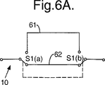
図4および図5にそれぞれ対応する図6および図7は、逆反射信号を位相変調する装置を示している。これは、図2および図3に示した例示的なマイクロストリップ・アレイに利用されている技術である。図6において、スイッチS1は伝送線10に沿って移動する信号を、一方が他方よりも物理的に長い2つの代替的パス61、62のうち一方に向けるために用いられ、そのスイッチが図6Aに示したその最も下の位置にあるか図6Bに示したその最も上の位置にあるかに応じて異なる移相につながる。既に述べたように、2つのパスのパス長は異なる。長い方のパス61のパス長は、パス62のパス長よりも波長の半分だけ長いことが有利であり、このことは2つの切替位置の間に最大の位相差を与え、そのため最も強い変調を与える。
【0047】
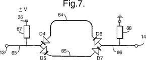
図7は、図6の回路をマイクロストリップにおいて実現できる方法を図式的に示している。端子13はマイクロストリップ63に接続されており、マイクロストリップ63はスイッチング・ダイオードD4の陰極およびスイッチング・ダイオードD5の陽極に接続されている。ダイオードD4の陽極はマイクロストリップ64に接続しており、ダイオードD5の陰極はマイクロストリップ65に接続している。マイクロストリップ64のパス長は、好ましくはλ/2だけマイクロストリップ65のパス長よりも長く、ここでλは伝送線における波長である。マイクロストリップ64の遠隔端はスイッチング・ダイオードD6の陰極に接続されており、マイクロストリップ65の遠隔端はスイッチング・ダイオードD7の陽極に接続されている。ダイオードD6の陽極とダイオードD7の陰極はマイクロストリップ66の一旦に接続しており、マイクロストリップ66はその他端で端子14に接続している。制御入力端子35は低域フィルタ67を介してマイクロストリップ63に接続されており、マイクロストリップ66は低域フィルタ68を介して接地に接続されている。
【0048】
使用に際しては、端子35に正の電位が印加されると、ダイオードD5およびD7はスイッチが入れられて、ダイオードD4およびD6はスイッチが切られ、それによって信号を短い方のマイクロストリップ65に沿って送り、同時にマイクロストリップ64を分離する。負の電位が端子35に印加されると、ダイオードD4およびD6はスイッチが入れられて、ダイオードD5およびD7はスイッチが切られ、それによって長い方のマイクロストリップ64に沿って信号を送り、同時にマイクロストリップ65を分離する。
【0049】
ここで、本発明に従って製作されたトランスポンダを示した図8を参照する。トランスポンダは、8対のダイポール・アンテナを含む逆反射アンテナ・アレイを含み、そのうち1対だけが、伝送線42によって相互接続された符号40、41で示されている。伝送線のそれぞれの長さIは次の式によって求められる。
【0050】
I=A±nλ
ここで、
A、nおよびλは上記のように定義されている。
【0051】
また、伝送線の少なくとも1本に関するnの値は、残りの伝送線のnの値に等しくない。
伝送線42に直列に接続されているのは、たとえば、図2および図3を参照してあるいは、図4および図5を参照して上記で説明した種類の変調装置43である。8個の変調装置のそれぞれへの制御入力は、個々の電流利得増幅器45を介して信号生成器44から提供される。増幅器45のそれぞれは、アンテナ対の間の伝送線における個々の変調装置で端子35に接続された個々の出力端子46から53を有している。
【0052】
任意選択で、センサまたは手動入力装置39を信号生成器に接続してもよい。部品39は、センサによって感知された何らかのパラメータおよび/または、キーボードまたはキーパッドなどの入力装置で手動入力された何らかの情報を表す信号を生成する。この信号は、変調がセンサまたは入力装置39からの過渡的情報を伝えるように、信号生成器44の出力の何らかのパラメータに影響する。トランスポンダが継続的に呼掛けされない場合には、次の呼掛けが行われるまで、部品39からの信号をメモリ手段(図示せず)に一時的に記憶することができる。
【0053】
信号生成器44から出力された方形波は、変調装置43のそれぞれを同じ状態、すなわち、図4A/6Aまたは図4B/6Bのいずれかに示した状態に同時に置くように動作可能である。そのため、図4および図5に示した振幅変調装置の場合には、アレイ全体が信号生成器の周波数で周期的に反射と吸収との間で切り替わる。したがって実際には、信号生成器はアレイから反射された信号を振幅変調し、変調の周波数は信号生成器の周波数である。同様に、図6および図7に示した位相変調装置の場合には、アレイは信号生成器の周波数で周期的に1つの位相と別の位相との間で切り替わる。したがって実際には、信号生成器はアレイから反射された信号を位相変調し、変調の周波数は信号生成器の周波数である。
【0054】
図8に示したトランスポンダも、「ダーク」アレイとして動作させることができる。たとえば、図4および図5に示した回路と共に用いられると、信号生成器44は、スイッチS1を図4Bに示した位置に永久に切り替えるように動作可能な一定の極性信号を印加して、それによって伝送線42に沿って通過する信号の吸収につながる。これらの状況の下で、アレイは、そのレーダー・サインを最小化するために用いることができるゼロまたは低反射性の状態にある。この状態において、低反射性の状態はアンテナ40、41の帯域幅によって制限された帯域幅である。
【0055】
同様に、トランスポンダが図6および図7の回路と共に用いられると、アレイは「ダーク」アレイとして動作するように製作することができる。これは、半分がもう半分と比較して逆位相で適用されるように、位相変調装置43に印加される制御信号を変調することにより達成できる。これらの状況において、アレイの半分によって生成された変調積は、もう半分によって生成された変調積に対して逆位相であり、ゼロまたは低反射につながる破壊的な干渉が全ての視角について生ずる。やはり装置は、伝送線42に沿って移動する波の波長ならびに、nが整数である場合の(n+1/2)で帯域幅限定されている。
【0056】
ここで、反射表面の上1/4波長で水平に整列されて0.61波長の間隔を開けられた、反波長ダイポールの4x4マトリックスからなるアンテナ・アレイに基づいて、トランスポンダ上で実行されたテストの結果を説明する。
【0057】
動作周波数は2.5GHzであり、ダイポール長はその放射効率を改善するためにλ/2から若干削減した。接地平面はダイポールに平行な軸に沿って32cmと計測され、直交軸に沿って28cmと計測された。モノスタティックRCSの計測は、遮蔽室に整列したレーダー吸収剤泡の使用によって促進された低反射環境において、ネットワーク・アナライザをソースおよび受信機として用いて行った。最終的な原型の変調は、高反射および低反射の状態の間で切り替えることにより達成された(すなわち、振幅変調)。第2の原型アレイも製作され、そこでは同軸伝送線が、相手方のアンテナに送られる代わりに吸収負荷によって終端とされた。やはり、RCSを計測して、逆アレイと比較した。高変調指数を達成するために、RCSの大きな変化を2つの原型の間で探した。結果の見本を図11に示した。
【0058】
これらの計測値は、逆アレイに必要とされる特性、すなわち、視角と共に緩やかに変化する高いRCSを示した。RCSが、入射RFに対するa)0°の高さ方向の回転(すなわち垂直)およびb)20°の高さ方向の回転で、アレイの方位回転の関数として表示されている図10を参照。RSCは、アレイ接地板と同じ形状の金属板の最大RSCに相対的に示されている。
【0059】
RCSの強い変化が達成できることを示したので、第3の原型アレイを、図4および図5を参照して上記で説明した方法で、切替回路が接地板の背後で同軸線に付加されたところに製作した。
【0060】
第3の原型を製作して、装置を逆反射状態および低反射状態の間で電気的に切り替えることができることを確認するために、モノスタティックRCSの計測を繰り返えした。
【0061】
次のテストには、2.5GHzに近いRFをアレイに照射するためにトランシーバを用い、反射信号の性質を検査して、図8の符号44で示したような信号生成器からの低周波数(通常25KHz)でアレイを振幅変調することが関係した。変調波形は方形波の波形と近似した。反射信号がスペクトル・アナライザに表示されると、図12に示したように反射RFの振幅変調によって生成された側波帯が明らかに見えた。
【0062】
図12から、方形波AMによって生成された側波帯は強力に見えることが分かる。また、搬送周波数Fcで返されるパワーは、環境に対するアレイの位置に強く依存するが、上側側波帯(USB)のうち最初の側波帯におけるパワーは依存しない。これは、変調積に利用可能な出力はアレイのRCSに依存し、一方、搬送周波数で返されるパワーはアレイ、環境および、それらの間には定在波が存在するのでそれらの相対的位置に依存するためである。
【0063】
図12Aに示したケースでは、アレイは受信搬送パワーについて極大であり、一方、図12Bに示したケースでは、アレイは3cm(1/4波長)だけ移動されて、搬送パワーの最小(19dBの削減)が結果として生じた。側波帯パワーは、距離の小さな変化によって非常に弱い影響だけを受ける。これは、クラッターがある環境における変調散乱体の強化された検知能を示している。
【0064】
アレイと入射RFとの間の向きは方位角(H平面)においてアレイを回転させることにより変えられたので、変調積を検討した。逆アレイについて予期したように、反射されたパワーは方位角と共にゆっくりと変化した。図13は、アレイが入射する照射に対して35度であるときに強く検出可能なままであり、最初の上側側波帯(USB)のパワーは、図12の「オン・ボアサイト」に比較して4dBだけ減少した。
【0065】
上記と同じアンテナ形状であるが、図6および図7を参照して上述した様式で移相スイッチを用いるさらなるアレイが構築された。マイクロストリップの2つの長さの間の理論上の位相差は、2.5GHzにおいて180度である。8個の位相スイッチが製造され(ダイポール対ごとに1つ)、測定される典型的な移相は2.5GHzで164度±2度であった。デジタル移相変調は、±1Vの振幅の方形波を各スイッチの端子35に加えることでなされた。図14は、この場合における変調積を示す。
【0066】
振幅変調アレイのように、位相変調アレイは、側波帯パワーが照明信号に対するアレイの向きに伴ってゆっくりと変化することを示した。アレイが0度から35度の方位角回転した場合、最初の上側波帯パワーは3dB減少した。最初の上側波帯パワーはまた、−35度から35度までの任意の方位角について、AMによって生成されるものよりも3〜5dB大きくもあった。大きな側波帯パワーの生成は、AMと比較して位相変調(PM)では一貫しており、AMは変調信号の交替サイクルにおける抵抗負荷にエネルギがダンプされるため、エネルギ効率がより低い。したがって、結果は、この用途では位相変調が有利なことを実証した。
【0067】
次に、上記した変調装置に対する代替の変調装置を示す図9を参照する。装置は樹状シーケンス発生器として説明することができ、RF入力/出力端子13、14を既に述べたように備え、これによって伝送線10(図示せず)に接続される。
【0068】
装置は、端子13に入力され端子14で出力されるかまたはその逆かに関わらず、信号は等しく扱われるという意味において対称的であるものであるが、本説明のために、入力信号は端子13に加えられるものと想定する。信号はまずスプリッタ/結合器70に渡され、ここで信号が複数(図示の例では3つ)の経路に分割される。各経路は、スプリッタ/結合器57において再結合される前に、それぞれの遅延装置54、55、または56において遅延を受ける。再結合された信号は端子14に渡される。
【0069】
遅延装置は、信号を遅延するよう動作可能な能動回路または受動回路を含んでも、または分散装置を含んでもよい。後者を実現する最も便利な方法は、単に3つの分岐それぞれについて2つのスプリッタ間の経路の長さを別にすることである。集中能動回路の一例はシフトレジスタである。
【0070】
樹状シーケンス発生器は、パルスレーダまたは連続波レーダ(CW)と併せて使用することができる。パルスレーダを用いる場合、各入力パルスが、要求されるバイナリワードにおけるデジタル「1」(パルスの欠如はデジタル「0」としてとられる)の位置に対応しうる特定の時間期間分遅延される。したがって、逆反射信号は一連のパルスからなり、この正確なパターンは、樹状分岐の数およびその個々の遅延時間によって判断することができる。CWレーダを用いる場合、システムは、所与の位相遅延を有する位相変調装置として動作する。
【0071】
双方の場合、復調は、樹状シーケンス発生器に対して共役作用を有する装置により受信器(図示せず)で実行されるため、アレイからの符号化リターン信号を復号化することができる。
【0072】
樹状シーケンス発生器に対する同様の作用はタップ付遅延線により達成することができ、その一例を図10に示し、次にこれを参照する。
タップ付遅延線は、実際に59で折り返され、図9の樹状シーケンス発生器内の対応する端子と同じ方法で接続されると共に、同じ機能を果たす入力/出力端子13および14で終端する単一伝送線58であるものを使用する。折り返された伝送線は線形であってもよいが、図示のように螺旋のものはスペースの節約をもたらす。線の長さに沿った間隔で、エネルギを伝送線の他方の半分に結合するカプラ60が設けられる。図面において、これらカプラは、折り返した2つの伝送線の半分の間の間隔が狭い短いセクションとして表される。これらカプラの構築は当業者には周知であり、能動的であっても受動的であってもよい。たとえば、カプラ60は、単に、伝送線58の2つの半分間の局所間隔を変化させることで実現することができ、螺旋のものでは、連続した螺旋のターンの間の間隔を変化させることができる。
【0073】
カプラ60は離間され、そうすることで伝送線の一方の半分における特定のポイントからエネルギを抽出し、それを伝送線の他方の半分における特定のポイントに再挿入することが分かろう。したがって、信号が遅延される量は、信号が端子13から端子14に、またはその逆に移る際に渡らなければならない伝送線の全長により決定される。中間点59を介して伝送線の全長に沿って渡った入力信号の成分は、最大量遅延される。したがって、出力信号は本質的に、すべて異なる遅延時間を有する複数の入力信号のコピーからなる。出力信号は、理論上、遅延線の代数的記述によって決定される任意の形状を有することができる。
【0074】
既に述べたように、復調は、受信器において共役装置、たとえば相関器として機能している別のタップ付遅延線によって実行される。
図9および図10の実施形態は双方とも、受動コンポーネントとして全体的に実現することが可能である。これは、特定の用途では必要であるかまたは有利でありうるが、装置を構築するときに変調が設定され、その後は容易に変えることができない場合には不利である、パワー消費がゼロであるという潜在的な利点を有する。しかし、遅延装置54〜56またはカプラ60を非常に低いがゼロではないパワーを用いて回路の内外で切り換えることができ、これにより、トランスポンダのサービス寿命中の変調の変更に対する備えを設備に提供する。かかる変更は、遠隔的に実行することも、機器に直接アクセスすることで行うことも可能である。
【0075】
次に、空港用の車両追跡システムを示す図15を参照するが、港における海洋船や混雑する航路等類似する状況に同じ概念を用いることが可能である。システムは追跡すべき車両90を含む。この車両は、空港を動き回り、航空機に対して潜在的な危険を引き起こしうる多様な陸上用車両の1つであることができ、実際には航空機自体であってもよい。他の車両、航空機、建造物、および種々雑多の構造物のクラッタが入った背景がある中で、車両90を追跡する必要があるものと想定する。このクラッタのある背景は、影を付けた長方形91で表される。
【0076】
追跡は、アンテナ93を備えるレーダトランシーバ92によって実行される。これは既知の技術であり、詳細には説明しない。
トランシーバ92内の送信器は、搬送周波数Fcにおいてレーダ信号がカバーすべき大まかなエリア全般を照明するように動作可能である。通常、用いられる周波数は、この目的のために利用可能な通常の周波数の1つ、たとえば2.5GHz ISM帯、9.4GHz海上帯、またはヒースロー空港の地上移動レーダによって用いられる16GHz帯である。
【0077】
矢印94および95は、車両90および背景91それぞれからの反射信号Fcを表す。図15Aでは、車両にはトランスポンダが装備されていないか、または装備されていても非変調タイプのものであると想定する。この場合、車両90および背景91からの反射信号の周波数スペクトルは、上部参照96に示されるパワー/周波数トレースに示される単一線に実質的に併合される。車両90による反射をクラッタのある背景91による反射から分離することは困難であることが分かろう。
【0078】
図15Bでは、車両11に、上記説明し図示したタイプ等の変調逆反射体を備えたトランスポンダが装備されており、その結果、変調周波数Fmにおいて変調された成分が車両90からの逆反射信号に加えられる。背景91からの反射信号は勿論この変調による影響を受けるため、受信器において、車両90を背景から容易に区別することができる。この場合の受信スペクトルは、パワー/周波数トレース97に示されている。受信器はオプションとして、残余表面クラッタは逆反射アクションによって低減されるが、これを拒絶するために、整合フィルタを備えてもよい。
【0079】
掃引周波数により照明される変調逆反射体の組み合わせは、クラッタのある環境において正確にレンジングする潜在性を与える。このようなシステムを図16に示す。
【0080】
システムは、トランシーバ98の形態のインテロゲータと、トランスポンダ100の部分を形成する変調逆反射体99とを備える。トランスポンダ100は、検出すべき固定のまたは可動の物体(図示せず)に取り付けることができる。トランシーバ98は、送信器101と、関連する送信アンテナ102とを備え、これらは共に、システムがカバーすべきエリアを照明する掃引周波数RF信号を送信する。送信される周波数は、たとえば、送信器101を表すボックス内の周波数/時間のグラフに示されるように、鋸歯状に掃引されうる。
【0081】
送信された信号は、特に逆反射体99を含むカバーエリア内のすべてのターゲットによって反射される。逆反射体99からの反射信号は、トランスポンダ100の部分をさらに形成するコード発生器103によって変調される。
【0082】
反射信号は受信アンテナ104で受信され、トランシーバ98の受信器セクションに入力される。ここで、入力RF信号は、RFミキサ105において、送信器101から出力される掃引周波数送信信号と結合される。これは、レーダの実施では従来的なことである。ミキサ105から出力される差分信号Δfは、時間間隔に正比例するため、送信された信号と受信された信号の間の経路の長さ2Lは:
【0083】
【数1】
Δf=(FstopーFstart)/Tsweep・2L/c
式中、FstartおよびFstopは、送信された信号の線形周波数ランプの開始周波数および終了周波数それぞれであり、これは時間間隔Tsweepにわたって繰り返され、cは光の速度である。
【0084】
クラッタのあるまたは多重経路環境においては、小さなRCSの特定ターゲットを識別することは困難である。差周波数Δfの典型的な値は、数Hzから2〜3KHz(可聴周波数)までである。
【0085】
ミキサ105からの出力はさらなるミキサ106に加えられ、ここで信号はコード発生器107からの出力と結合され、その出力はコード発生器103の出力を反映するため、参照104下に示す範囲/周波数のグラフで表されるように、ターゲットから生じる差周波数を回復することができる。このプロセスは、おそらく変調周波数に近いΔfの値を生成する非常に広い範囲におけるものを除き、すべての他のターゲットを効果的に拒絶する。
【0086】
差周波数Δfよりもはるかに高い周波数(fmod)を有するように選択される一定期間の方形波で変調される単純な場合を考える。この場合、第1のミキサ105の出力における差周波数は、逆反射体99からの反射により、Δf+fmodで与えられる。コヒーレント検波のため、第2のミキサを搬送波回復段階と併せて用いてもよい。第2のミキサ106において、差周波数Δfは、逆反射体99からの反射により、回復される。あるいは、当該トランスポンダの変調周波数でセンタリングされた帯域フィルタが前置される包絡線検波器等、インコヒーレント検波方法を使用してもよい。上記を除き、他のターゲットからの反射は拒絶される。
【0087】
実際には、用いられる変調は上述した単純な性質でない場合がある。たとえば、擬似乱数コードを変調波形として加えることで、技法を改良することができる。変調はスペクトル拡散であることができ、この場合、直接シーケンス拡散コードが用いられれば、信号を回復するために、インテロゲータはトランスポンダ上のコードを知る必要がないであろう。
【0088】
図17は、9.0GHzと9.4GHzの間の掃引搬送波および1MHz方形波で位相変調される16素子逆反射体を用いて、屋内環境で上述した技術を用いて回復された差周波数fの波形を示す。図17Aは時間領域を示し、図17Bは周波数領域を示す。FFTアルゴリズムは、この場合では3.80mのターゲット範囲に相当する355Hzにおいて強い周波数成分をはっきりと示した。実験では背景反射を低減する試みは行われなかった。
【0089】
図16を参照して説明したシステムの変更において、複数の離間された変調逆反射体が用いられる。たとえば、3個の逆反射体と、単一のインテロゲータは、3次元範囲の三角測量を提供することができる。このようなシステムにおける受信器には、各逆反射体に対する範囲を計算できるように、各逆反射体に1つずつ複数の局部発振器が取り付けられる。このようなシステムの精度は、勿論、逆反射体の分離および範囲によって決まる。実際には、リンクの容量が許せば、全地球位置/システムのようになり同様の制約を受ける。システムは逆にも、すなわち3個の離間したインテロゲータと単一の変調逆反射体を用いて3次元範囲の三角測量を提供することも可能である。
【図面の簡単な説明】
【図1】 Van Attaタイプの一次元逆反射アンテナ・アレイの略側面図である。
【図2】 本発明のトランスポンダに用いられる、4x4マイクロストリップ・アンテナ・アレイの略平面図である。
【図3】 図2のマイクロストリップ・アレイの反対側の略平面図であり、逆側面上の相互接続を示している。
【図4】 振幅変調を達成するのに用いられる回路の略図である。
【図5】 図4の変調回路をより詳細に示した図である。
【図6】 図4に対応するが、位相変調を達成するために用いられる回路の例を示している。
【図7】 図5に対応するが、位相変調を達成するために用いられる回路の例を示している。
【図8】 16素子逆反射アンテナ・アレイを内蔵したマイクロ波トランスポンダのブロック図である。
【図9】 代替的な変調装置を示したブロック図である。
【図10】 代替的な変調装置を示したブロック図である。
【図11】 本発明に従って製作され、図8に示したような4x4逆反射アンテナ・アレイを内蔵したトランスポンダで実行されるテストの結果を示したグラフである。視角でアレイRCSの変化を示しており、実線は連結されたダイポール対(逆反射)を示し、点線は50Ωの負荷がかかったダイポールを示している。
【図12】 本発明に従って製作され、図8に示したような4x4逆反射アンテナ・アレイを内蔵したトランスポンダで実行されるテストの結果を示したグラフである。アレイ・ボアサイトに対して0°方位角で、振幅変調されて反射されたRF波の側波帯反応を示している。
【図13】 本発明に従って製作され、図8に示したような4x4逆反射アンテナ・アレイを内蔵したトランスポンダで実行されるテストの結果を示したグラフである。図12に対応しているが、アレイ・ボアサイトに対して35°方位角での反応を示している。
【図14】 本発明に従って製作され、図8に示したような4x4逆反射アンテナ・アレイを内蔵したトランスポンダで実行されるテストの結果を示したグラフである。図12に類似の図であるが、アレイ・ボアサイトに対して0°方位角(A)および35°方位角(B)での位相変調され反射された波にの側波帯反応を示している。
【図15】 本発明に従って製作され、図8に示したような4x4逆反射アンテナ・アレイを内蔵したトランスポンダで実行されるテストの結果を示したグラフである。空港で用いられる乗り物追跡システムにおける、本発明の変調トランスポンダの1つの応用を示している。
【図16】 本発明の変調トランスポンダを内蔵したレーダー・システムの図である。
【図17】 図16に示したシステムで実行されたテストの結果を示したグラフである。[0001]
The present invention relates to transponders, and more particularly to transponders using antenna-based retroreflectors and position / tracking systems utilizing such transponders.
[0002]
A retroreflector is a device that reflects incident radiation poured onto it on its incident path. Although it is known to use retroreflectors as the basis for active or passive transponders, the underlying principle is to establish a communication link by reflecting the interrogation signal towards its source. , Thereby eliminating the need for transmitters and their associated equipment at the target.
[0003]
In the application of radar to ground traffic control, there is a growing need to detect, track and identify aircraft within the surveillance area. This is particularly relevant for port and airport traffic management, especially when considering small vehicles with a small radar effective reflection cross section (RCS). Currently, simple retroreflectors including corner structures may be used in small vessels to increase their RCS. Clearly, future transponders used in these fields require simplicity, light weight, low cost and low power consumption.
[0004]
In the past, extensive identification has been achieved by actively sending responses to the interrogation radar. Such a method is used by the military “Interrogate Friend or Foe” (IFF) system, but the disadvantage of this approach is that it requires a transmitter or signal processing device to be installed on the target. Also, since the response signal is transmitted in all directions, an excessively large transmission power is required to establish a communication link, and the local radio environment is damaged.
[0005]
It is known to use a retroreflective antenna array in a transponder. Such an array is based on the Van Atta array first described in US Pat. No. 2,908,002. The Van Atta array includes an array of unidirectional or multidirectional antennas in which antenna pairs are coupled by transmission lines of uniform electrical length. FIG. 1 of the accompanying drawings shows a unidirectional Van Atta array including six dipole antennas 1-6. The dipoles are connected in pairs by individual transmission lines as follows.
[0006]
Dipoles 3 and 4 are connected by a transmission line 9
Transmission lines 7, 8 and 9 are all of uniform electrical length, and as a result of such coupling, indicate that electromagnetic wave destinations A to F incident on the array are reflected back from the array along the direction of incidence. be able to.
[0007]
Assuming a plane wave incident on the x-axis at an angle (assuming that the point A to F is taken as the incident wave destination, the energy from the point A is received by the
[0008]
Problems arise in practical use of the Van Atta array because all of the transmission times need to be the same electrical length. For example, creating a bi-directional planar array is nearly impossible if the extra complexity and cost of crossover is avoided.
[0009]
In the first aspect of the invention, this problem is avoided by defining that the length of the transmission line interconnecting the individual antennas in the array is a length I determined by the following equation:
[0010]
I = A ± nλ
here,
A is an arbitrary length,
n is zero or an integer;
λ is the wavelength of the electromagnetic waves that are reflected back.
[0011]
If n = 0 for all transmission lines, this effectively defines Van Atta, since all transmission lines in such an array are of any uniform length. Therefore, the present invention further defines that at least some of the transmission lines have a non-zero value n. Thus, unique to the present invention is that not all transmission lines are the same length.
[0012]
Extending any one of the transmission lines 7 to 9 by an amount equal to a multiple of the wavelength of the received signal means that when the transmission signal reaches the plane A-F, the corresponding transmission line is not extended. Has the same phase as would have had. Thus, the power from each antenna is still putatively summed in the direction (and the array continues to operate retroreflectively.
[0013]
However, since the phase of plane A-F is reached only when the extra length of interconnecting transmission lines is a multiple of the received wavelength, this configuration is sensitive to frequency. While this may be understood to be a drawback, it is often an advantage in practice, especially in defense and military applications, as it provides small but extra security. In practice, it is not difficult to use a single interrogation frequency, especially when keeping in mind that the antenna itself is already frequency selective. In addition, the device can act as a filter that returns a single frequency or, practically, only the passband frequency, to the interrogating transceiver.
[0014]
Using non-uniform length transmission lines, as described above, makes the two-dimensional retroreflective antenna array any of known planar media such as microstrips, striplines or dielectric or optical waveguides. Allows the array to be fabricated in a conventional cavity waveguide. Even if the array is non-planar, the fact that several transmission lines can be different in length from other transmission lines greatly increases the physical design problem of interconnecting antenna pairs in a two-dimensional array. To reduce. Indeed, the present invention provides almost complete freedom regarding the length of the transmission line, which greatly assists in the design process. Obviously, however, there is an upper limit on the length beyond which transmission line loss becomes unacceptable. Also, the large difference in length causes a difference in loss characteristics between different transmission lines that may degrade operation if excessive.
[0015]
Under the above constraints, the length A can be chosen literally arbitrarily and can be zero, but the zero value imposes a meaningless limit on the length of the transmission line. That is, all transmission line lengths must be equal to multiples of wavelengths. More well, length A can be either the smallest or largest convenient physical length, and the remaining length is the same as any length, due to physical or other constraints. If this is not possible, then it should be longer or shorter than any length by an amount equal to an integer multiple of the wavelength. Thus, any one array can have only one or two transmission lines that are different in length from the other transmission lines, and in the other extreme case any one transmission line. But of course all can have different lengths according to the length formula quoted above.
[0016]
In an embodiment of the present invention, means are provided for modulating the retroreflected signal so that the target can identify itself to the interrogator. The modulating means may comprise a modulation device connected in at least some, preferably all, of the transmission lines to modulate signals passing from one antenna of the array to another through the transmission line. Convenient. Each modulation device can include active or passive circuitry.
[0017]
The modulating means can be realized by any device operable to modulate a signal in order to generate a modulation product in the frequency domain. Thus, in order to achieve amplitude modulation or frequency / phase modulation, modulation may include switching in the time domain, splitting the signal, delaying the split component by the amount of change, and reducing the delayed component Various forms of recombination may be included to generate a multiplexed signal that includes the sum of the individual components. In all cases, the modulation process produces a modulation product in the frequency domain.
[0018]
Such transponder applications include ground radar for vehicle identification and search, avionic landing systems, earth and space communications, local area networks, and port and airport management that needs to track a large number of small vehicles. Includes ground traffic control. Other applications include satellite systems, remote sensing, road vehicle systems and general maritime applications. For example, transponders can be attached to maritime or avionics navigation beacons such as buoys and lighthouses. If the retro-reflected signal is modulated with a code unique to the target, the target can identify itself to the interrogator. Alternatively, the modulator provides means for frequency modulating the retro-reflected signal to mimic a Doppler shift to make the target appear to be moving when it is not actually moving, or vice versa. Can be included.
[0019]
In an embodiment of the invention, the modulation device comprises switching means controlled by a modulation signal, said switching means receiving signals for a plurality of paths including circuit elements, some of which are operable to change the parameters of the signal. Are periodically operable to modulate the signal at the frequency of the modulation signal. For example, the circuit element can include means for modifying the amplitude or phase of a signal traveling along the transmission line, thereby generating an amplitude or phase modulated wave.
[0020]
In an embodiment, in order to achieve amplitude extension, the switching means absorbs the received signal, a direct current connection through which the signal passes through the device with substantially unchanged amplitude, and, in whole or in part, absorbs the signal. It is possible to operate so as to connect alternately to the load. Similarly, to implement phase modulation, the switching means is operable to connect the received signal alternately between two paths of different path lengths. The difference between these path lengths is preferably half the wavelength of the received signal. The switching means preferably includes a semiconductor switch such as a switching diode.
[0021]
In an alternative embodiment of the invention, the modulation device operates to split the received signal into at least two paths and to change some parameter of the signal connected to each path and passing along the path. Possible circuit elements. Also, a coupling means for recombining signals from the individual paths is provided. These circuit elements take the form of delay elements, the configuration of which is related to the different paths so that the recombined signal is the sum of the original signals passing along the transmission line delayed by different amounts. It is preferable that the delay times are set differently.
[0022]
So far, the modulation means can provide information to the retro-reflected signal, but this information is basically fixed by the characteristics of the modulation means and includes, for example, identification information identifying the article to which the transponder is attached. Was supposed to be possible. However, in an embodiment of the invention, the modulation means may have transient information in addition to or instead of the “fixed” information described above. To that end, the transponder can further include variable input means such as a sensor that generates a signal indicative of some parameter, possibly related to the environment local to the transponder. This signal is passed to the modulation means in order to change the modulation in some way according to the signal. Thus, for example, if the transponder is on a moving object, the sensor will receive not only “fixed” information from which the interrogating transceiver identifies the object, but also transient information indicating its position from the transponder. In addition, a signal indicating the position of the object can be generated. The sensor may also detect local temperature or pressure or the presence of abnormal equipment.
[0023]
The method by which the signal from the sensor acts on the modulation depends on the type of modulation used and the nature of the sensor signal itself.
The variable input means may alternatively or additionally include some form of manual intervention device. To that end, the variable input means can include an input device such as a keyboard or keypad that can be used to input information affecting the modulation means to change the modulation signal. In this way, a person in the vicinity of the transponder can transmit a message via a retroreflected signal. Such messages can be stored locally in memory until such time as the interrogating transceiver sweeps the transponder.
[0024]
In yet another embodiment of the present invention, amplifying means are provided on at least some of the transmission lines, preferably all, in order to amplify signals passed from one antenna of the array to another through the transmission line. Provide. Such amplifying means is preferably bidirectional, i.e. it can amplify signals moving in either direction.
[0025]
The amplifying means can be used instead of or in addition to the aforementioned modulating means, but in practice the amplifying means is itself adjusted to provide both functions in a single unit. .
[0026]
In yet another aspect of the invention, a fixed or object position / tracking system is provided, the system transmitting at least one modulation transponder and a signal for radiating to the transponder or each transponder. A transmitter, a receiver that receives a retroreflected signal from one or more transponders, and a discriminating means in the receiver that demodulates the modulated signal from the one or more transponders to identify a desired reflected signal; including.
[0027]
For example, each transponder can be attached to a fixed or moving object that locates. Alternatively, multiple spaced modulation transponders can be used to achieve ranging.
A special realization of such a system is a vehicle position / tracking system for airports, for example in the form of vehicles such as airport service vehicles or airplanes that are guided or landed (blind aircraft landing systems). For this purpose, a modulated retroreflector is mounted so that the position can be easily ascertained by the associated illumination transmitter and interrogation receiver. Since modulation can provide a distinct radar "signature" that can be identified, the use of modulation greatly improves the receiver's ability to discriminate the desired vehicle from a cluttered background.
[0028]
In an embodiment, ranging information is provided by sweeping the frequency of the illumination transmitter. The target in this case includes, for example, or includes a modulation retroreflector of the type described above.
In order to establish a dual communication link, a passive transponder (ie without a transmitter) is required to change its state in response to stimuli obtained from control signals contained within the irradiated radiation. There is a case. In order to meet the requirements for such bi-directional links, microwave retro-reflective antennas are very suitable for modulation. Because the array includes antennas and transmission lines that efficiently direct incident microwave radiation into the microstrip circuit (as opposed to optical corner type reflectors), this radiation has additional logic. It can be sampled and processed by a circuit. The transponder can then respond to the received control stimulus and change its modulation state accordingly.
[0029]
Transponders can be made self-powered in a manner similar to conventional radio tags, for example by incident radiation, but the collected energy is not re-radiated as RF, but passively Used only for moderate output requirements of the modulation circuit integrated in the array. Because high data rates (currently 10 MHz) are possible, transponders operating in this mode have a longer “quiet” or period of change compared to periods of energy consumption where modulation is facilitated, but still many. It can have an information transfer rate of Kbits / s. The required duty cycle is derived from the output link budget available in a given system application.
[0030]
In order that the present invention may be better understood, some embodiments thereof are described by way of example only and with reference to the accompanying drawings.
Referring first to FIG. 2, it is shown how a two-dimensional array can be realized using microstrip technology. The antenna array is fabricated on a
[0031]
Transmission line 75: 72.1 to 72.16
Transmission line 76: 72.2 to 72.15
Transmission line 77: 72.3 to 72.14
Transmission line 78: 72.4 to 72.13
Transmission line 79: 72.5 to 72.12
Transmission line 80: 72.6 to 72.11
Transmission line 81: 72.7 to 72.10.
Transmission line 82: 72.8 to 72.9
Connected in series with each of the transmission lines 75-82 is an amplifier (not shown) and / or a
[0032]
I = A ± nλ
here,
A is an arbitrary length,
n is zero or an integer;
λ is the wavelength of the electromagnetic wave.
[0033]
The value A is arbitrarily selected according to the above description, but once selected, it is the same for all transmission lines in a particular array. The length I is the total length from one antenna to another, and therefore includes the length of the connecting
[0034]
From FIG. 3, one convenient way to calculate the remaining length of the
[0035]
In determining the location of transmission lines 75-82, the crossover immediately implies the presence of additional layers of circuitry, increasing complexity and cost, and electromagnetic interaction if adjacent transmission lines are too close together. Therefore, it is desirable to avoid crossover.
[0036]
[0037]
The
[0038]
4 and 5 show an apparatus for amplitude modulating the retroreflected signal. A typical transmission line is indicated by
[0039]
FIG. 4 shows the switch S1 in two alternative positions. FIG. 4A shows a first position where the signal passes unaffected, and when the switch is in this position, the array operates as a normal retro-reflective array. FIG. 4B shows a second position where a signal approaching from the left of the drawing is switched into the
[0040]
FIG. 5 shows how the amplitude modulation circuit of FIG. 4 is realized on a microstrip measuring approximately 50 mm × 50 mm. The RF signal is exchanged with the circuit through
[0041]
The T-
[0042]
Forming a
[0043]
Interconnecting the two 50 Ω
[0044]
In use, the
[0045]
When a negative potential is applied to
[0046]
6 and 7 corresponding to FIGS. 4 and 5, respectively, show an apparatus for phase modulating the retroreflected signal. This is the technique utilized in the exemplary microstrip array shown in FIGS. In FIG. 6, switch S1 is used to direct a signal traveling along
[0047]
FIG. 7 schematically shows how the circuit of FIG. 6 can be implemented in a microstrip.
[0048]
In use, when a positive potential is applied to
[0049]
Reference is now made to FIG. 8, which shows a transponder made in accordance with the present invention. The transponder includes a retro-reflective antenna array that includes eight pairs of dipole antennas, only one of which is indicated by
[0050]
I = A ± nλ
here,
A, n and λ are defined as above.
[0051]
Also, the value of n for at least one of the transmission lines is not equal to the value of n for the remaining transmission lines.
Connected in series to the transmission line 42 is, for example, a
[0052]
Optionally, a sensor or
[0053]
The square waves output from the
[0054]
The transponder shown in FIG. 8 can also be operated as a “dark” array. For example, when used with the circuits shown in FIGS. 4 and 5, the
[0055]
Similarly, when a transponder is used with the circuits of FIGS. 6 and 7, the array can be made to operate as a “dark” array. This can be achieved by modulating the control signal applied to the
[0056]
Here, tests performed on a transponder based on an antenna array consisting of a 4 × 4 matrix of anti-wavelength dipoles aligned horizontally at a quarter wavelength above the reflective surface and spaced 0.61 wavelength apart The result of will be described.
[0057]
The operating frequency was 2.5 GHz and the dipole length was slightly reduced from λ / 2 to improve its radiation efficiency. The ground plane was measured as 32 cm along the axis parallel to the dipole and 28 cm along the orthogonal axis. Monostatic RCS measurements were performed using a network analyzer as the source and receiver in a low reflection environment facilitated by the use of radar absorbent foam aligned with the shielded room. Final prototype modulation was achieved by switching between high and low reflection states (ie amplitude modulation). A second prototype array was also fabricated, where the coaxial transmission line was terminated by an absorbing load instead of being sent to the other antenna. Again, RCS was measured and compared to the reverse array. In order to achieve a high modulation index, a large change in RCS was sought between the two prototypes. A sample of the results is shown in FIG.
[0058]
These measurements showed the characteristics required for the reverse array, ie, a high RCS that varies slowly with viewing angle. See FIG. 10 where the RCS is displayed as a function of the azimuthal rotation of the array with a) 0 ° height rotation (ie vertical) and b) 20 ° height rotation relative to the incident RF. RSC is shown relative to the maximum RSC of a metal plate of the same shape as the array ground plate.
[0059]
Having shown that a strong change in RCS can be achieved, the third prototype array can be added to the coaxial line behind the ground plane in the manner described above with reference to FIGS. Made.
[0060]
A monostatic RCS measurement was repeated to make a third prototype and confirm that the device can be electrically switched between the retro- and low-reflection states.
[0061]
For the next test, a transceiver was used to irradiate the array with RF close to 2.5 GHz, the nature of the reflected signal was examined, and a low frequency from a signal generator as shown at 44 in FIG. It was related to amplitude modulation of the array (usually 25 KHz). The modulation waveform was approximated to a square waveform. When the reflected signal was displayed on the spectrum analyzer, the sidebands generated by amplitude modulation of the reflected RF were clearly visible as shown in FIG.
[0062]
From FIG. 12, it can be seen that the sidebands generated by the square wave AM appear strong. Also, the power returned at the carrier frequency Fc strongly depends on the position of the array relative to the environment, but the power in the first sideband of the upper sideband (USB) does not. This is because the output available for the modulation product depends on the RCS of the array, while the power returned at the carrier frequency is relative to the array, the environment, and their relative position because there are standing waves between them. Because it depends.
[0063]
In the case shown in FIG. 12A, the array is maximal in terms of received carrier power, whereas in the case shown in FIG. 12B, the array is moved by 3 cm (1/4 wavelength) to minimize the carrier power (19 dB reduction). ) Resulted. Sideband power is only very weakly affected by small changes in distance. This demonstrates the enhanced detectability of the modulated scatterers in an environment with clutter.
[0064]
Since the orientation between the array and the incident RF was changed by rotating the array in the azimuth angle (H plane), the modulation product was considered. As expected for the reverse array, the reflected power changed slowly with azimuth. FIG. 13 remains strongly detectable when the array is at 35 degrees to the incident illumination, and the power of the first upper sideband (USB) is compared to “On Boresight” in FIG. And decreased by 4 dB.
[0065]
Additional arrays were constructed with the same antenna shape as above, but using phase shift switches in the manner described above with reference to FIGS. The theoretical phase difference between the two lengths of the microstrip is 180 degrees at 2.5 GHz. Eight phase switches were manufactured (one for each dipole pair) and the typical phase shift measured was 164 degrees ± 2 degrees at 2.5 GHz. Digital phase shift modulation was performed by applying a square wave with an amplitude of ± 1 V to the
[0066]
Like amplitude modulation arrays, phase modulation arrays have shown that the sideband power varies slowly with the orientation of the array with respect to the illumination signal. When the array was rotated from 0 degrees to 35 degrees azimuth, the initial upper sideband power decreased by 3 dB. The initial upper sideband power was also 3-5 dB greater than that produced by AM for any azimuth from -35 degrees to 35 degrees. The generation of large sideband power is consistent with phase modulation (PM) compared to AM, which is less energy efficient because the energy is dumped to a resistive load in the alternating cycle of the modulation signal. Thus, the results demonstrated that phase modulation is advantageous for this application.
[0067]
Reference is now made to FIG. 9, which shows an alternative modulator for the modulator described above. The device can be described as a dendritic sequence generator, comprising RF input /
[0068]
The device is symmetrical in the sense that the signals are treated equally regardless of whether they are input to
[0069]
The delay device may include active or passive circuitry operable to delay the signal, or may include a distributed device. The most convenient way to implement the latter is simply to separate the path length between the two splitters for each of the three branches. An example of a lumped active circuit is a shift register.
[0070]
The dendritic sequence generator can be used in conjunction with pulsed radar or continuous wave radar (CW). When using pulse radar, each input pulse is delayed by a specific time period that may correspond to the position of a digital “1” in the required binary word (the absence of a pulse is taken as a digital “0”). Thus, the retroreflective signal consists of a series of pulses, and this exact pattern can be determined by the number of dendritic branches and their individual delay times. When using CW radar, the system operates as a phase modulator with a given phase delay.
[0071]
In both cases, demodulation is performed at the receiver (not shown) by a device that has a conjugate effect on the dendritic sequence generator so that the encoded return signal from the array can be decoded.
[0072]
A similar effect on the dendritic sequence generator can be achieved with a tapped delay line, an example of which is shown in FIG.
The tapped delay line is actually folded at 59 and connected in the same manner as the corresponding terminals in the dendritic sequence generator of FIG. 9 and is simply terminated at input /
[0073]
It will be appreciated that the
[0074]
As already mentioned, the demodulation is performed by another tapped delay line functioning as a conjugate device, for example a correlator, at the receiver.
Both the embodiments of FIGS. 9 and 10 can be implemented entirely as passive components. This may be necessary or advantageous in certain applications, but is disadvantageous if the modulation is set when building the device and cannot be easily changed afterwards, zero power consumption Has the potential advantage. However, delay units 54-56 or
[0075]
Reference is now made to FIG. 15, which shows a vehicle tracking system for an airport, but the same concept can be used for similar situations such as marine ships and congested routes in a port. The system includes a
[0076]
Tracking is performed by a
The transmitter in the
[0077]
[0078]
In FIG. 15B, the
[0079]
The combination of modulated retroreflectors illuminated by the sweep frequency provides the potential for accurate ranging in cluttered environments. Such a system is shown in FIG.
[0080]
The system comprises an interrogator in the form of a
[0081]
The transmitted signal is reflected by all targets in the coverage area, particularly including the
[0082]
The reflected signal is received by receive
[0083]
[Expression 1]
Δf = (F stop -F start ) / T sweep ・ 2L / c
Where F start And F stop Are the starting frequency and ending frequency of the linear frequency ramp of the transmitted signal, respectively, which is the time interval T sweep C is the speed of light.
[0084]
In a cluttered or multipath environment, it is difficult to identify a specific target for a small RCS. Typical values for the difference frequency Δf range from a few Hz to 2-3 KHz (audible frequency).
[0085]
The output from
[0086]
A frequency much higher than the difference frequency Δf (f mod Consider the simple case of being modulated with a square wave of a certain period chosen to have. In this case, the difference frequency at the output of the
[0087]
In practice, the modulation used may not be as simple as described above. For example, the technique can be improved by adding a pseudo-random code as a modulation waveform. The modulation can be spread spectrum, in which case if a direct sequence spread code is used, the interrogator will not need to know the code on the transponder to recover the signal.
[0088]
FIG. 17 shows the difference in frequency f recovered using the technique described above in an indoor environment using a swept carrier between 9.0 GHz and 9.4 GHz and a 16 element retroreflector phase modulated with a 1 MHz square wave. Waveform is shown. FIG. 17A shows the time domain, and FIG. 17B shows the frequency domain. The FFT algorithm clearly showed a strong frequency component at 355 Hz, which in this case corresponds to a target range of 3.80 m. In the experiment, no attempt was made to reduce background reflection.
[0089]
In the system modification described with reference to FIG. 16, a plurality of spaced apart modulated retroreflectors are used. For example, three retroreflectors and a single interrogator can provide a three-dimensional range of triangulation. The receiver in such a system is fitted with a plurality of local oscillators, one for each retroreflector so that the range for each retroreflector can be calculated. The accuracy of such a system is, of course, determined by the separation and extent of the retroreflector. In practice, if the capacity of the link allows, it becomes like a global location / system and is subject to similar constraints. The system can also conversely provide triangulation in a three-dimensional range using three spaced interrogators and a single modulating retroreflector.
[Brief description of the drawings]
FIG. 1 is a schematic side view of a Van Atta type one-dimensional retroreflective antenna array;
FIG. 2 is a schematic plan view of a 4 × 4 microstrip antenna array used in the transponder of the present invention.
FIG. 3 is a schematic plan view of the opposite side of the microstrip array of FIG. 2, showing the interconnections on the opposite side.
FIG. 4 is a schematic diagram of a circuit used to achieve amplitude modulation.
FIG. 5 is a diagram showing the modulation circuit of FIG. 4 in more detail.
FIG. 6 corresponds to FIG. 4 but shows an example of a circuit used to achieve phase modulation.
FIG. 7 corresponds to FIG. 5, but shows an example of a circuit used to achieve phase modulation.
FIG. 8 is a block diagram of a microwave transponder incorporating a 16-element retroreflective antenna array.
FIG. 9 is a block diagram illustrating an alternative modulation device.
FIG. 10 is a block diagram illustrating an alternative modulation device.
11 is a graph illustrating the results of tests performed in accordance with the present invention and performed on a transponder incorporating a 4 × 4 retroreflective antenna array as shown in FIG. The change in the array RCS is shown by the viewing angle, the solid line shows the connected dipole pair (reverse reflection), and the dotted line shows the dipole loaded with 50Ω.
12 is a graph showing the results of tests performed in accordance with the present invention and performed on a transponder incorporating a 4 × 4 retroreflective antenna array as shown in FIG. The sideband response of an RF wave reflected amplitude modulated at 0 ° azimuth relative to the array boresight is shown.
FIG. 13 is a graph illustrating the results of tests performed in accordance with the present invention and performed on a transponder incorporating a 4 × 4 retroreflective antenna array as shown in FIG. Corresponding to FIG. 12, it shows the response at 35 ° azimuth to the array boresight.
14 is a graph illustrating the results of tests performed in accordance with the present invention and performed on a transponder incorporating a 4 × 4 retroreflective antenna array as shown in FIG. FIG. 13 is a view similar to FIG. 12 but showing the sideband response to a phase modulated and reflected wave at 0 ° azimuth (A) and 35 ° azimuth (B) with respect to the array boresight. Yes.
15 is a graph illustrating the results of tests performed in accordance with the present invention and performed on a transponder incorporating a 4 × 4 retroreflective antenna array as shown in FIG. Figure 2 illustrates one application of the modulation transponder of the present invention in a vehicle tracking system used at an airport.
FIG. 16 is a diagram of a radar system incorporating the modulation transponder of the present invention.
FIG. 17 is a graph showing the results of tests executed by the system shown in FIG.
Claims (28)
各前記伝送線の長さlは、l=A±nλによって与えられ、
式中、Aは任意の長さであり、nはゼロまたは整数であり、λは逆反射すべき電磁波の波長であり、
少なくともいくつかの伝送線についてのnの値は残りのものとは異なる、
トランスポンダ。A transponder comprising an array of antennas interconnected in pairs so as to be retro-reflected by a transmission line, each said plurality of pairs comprising two antennas arranged symmetrically with respect to the center point of said array So that at least some of the transmission lines that are different in length from the remaining transmission lines provide a two-dimensional retroreflection of the array, and all of the transmission lines are from one antenna of the pair to the other of the pair Arranged to be passed to the other antenna without crossing any of the other transmission lines,
The length l of each said transmission line is given by l = A ± nλ,
Where A is any length, n is zero or an integer, λ is the wavelength of the electromagnetic wave to be retro-reflected,
The value of n for at least some transmission lines is different from the rest,
transponder.
前記変調トランスポンダは、伝送線により逆反射になるように複数の対で相互接続されるアンテナのアレイを備え、各前記複数の対は前記アレイの中心点に関して対称的に配置された2つのアンテナを含み、残りの前記伝送線と異なる長さである少なくとも幾つかの前記伝送線に二次元の前記アレイの逆反射を与えるように、そして前記伝送線の全ては対の一方のアンテナから前記対の他方のアンテナへ前記伝送線の他のいずれとも交差することなく渡されるように配列され、
各前記伝送線の長さlは、l=A±nλによって与えられ、
式中、Aは任意の長さであり、nはゼロまたは整数であり、λは逆反射すべき電磁波の波長であり、
少なくともいくつかの伝送線についてのnの値は残りのものとは異なる、
システム。A fixed or movable object positioning / tracking system comprising at least one modulation transponder, a transmitter for transmitting a signal to illuminate said modulation transponder or each modulation transponder, and modulation transponder (s) A receiver for receiving the retro-reflected signal and a discriminating means in the receiver for demodulating the modulated signal from the modulation transponder (s) so that the required reflected signal can be identified; The transmitter comprises means for sweeping the transmission output frequency ;
The modulation transponder comprises an array of antennas interconnected in pairs so as to be retroreflected by a transmission line, each of the plurality of pairs comprising two antennas arranged symmetrically with respect to the center point of the array Including at least some of the transmission lines that are different in length from the remaining transmission lines so as to provide a two-dimensional back reflection of the array, and all of the transmission lines are connected from one antenna of the pair Arranged to pass to the other antenna without crossing any of the other transmission lines,
The length l of each said transmission line is given by l = A ± nλ,
Where A is any length, n is zero or an integer, λ is the wavelength of the electromagnetic wave to be retro-reflected,
The value of n for at least some transmission lines is different from the rest,
system.
Applications Claiming Priority (5)
| Application Number | Priority Date | Filing Date | Title |
|---|---|---|---|
| GBGB9907117.7A GB9907117D0 (en) | 1999-03-26 | 1999-03-26 | Transponder |
| GBGB9912840.7A GB9912840D0 (en) | 1999-06-02 | 1999-06-02 | Transponder |
| GB9912840.7 | 1999-06-02 | ||
| GB9907117.7 | 1999-06-02 | ||
| PCT/GB2000/001136 WO2000059068A1 (en) | 1999-03-26 | 2000-03-24 | Transponders |
Publications (2)
| Publication Number | Publication Date |
|---|---|
| JP2002540704A JP2002540704A (en) | 2002-11-26 |
| JP4588220B2 true JP4588220B2 (en) | 2010-11-24 |
Family
ID=26315348
Family Applications (1)
| Application Number | Title | Priority Date | Filing Date |
|---|---|---|---|
| JP2000608468A Expired - Fee Related JP4588220B2 (en) | 1999-03-26 | 2000-03-24 | transponder |
Country Status (6)
| Country | Link |
|---|---|
| US (1) | US6657580B1 (en) |
| EP (1) | EP1166388B1 (en) |
| JP (1) | JP4588220B2 (en) |
| AT (1) | ATE253774T1 (en) |
| DE (1) | DE60006370T2 (en) |
| WO (1) | WO2000059068A1 (en) |
Families Citing this family (43)
| Publication number | Priority date | Publication date | Assignee | Title |
|---|---|---|---|---|
| TW594965B (en) * | 2003-09-10 | 2004-06-21 | Goyatek Technology Inc | Power supply layout structure of integrated circuit |
| WO2005088850A1 (en) * | 2004-03-17 | 2005-09-22 | Brother Kogyo Kabushiki Kaisha | Position detection system, response device and query device, radio communication system, position detection method, position detection program, and information recording medium |
| US7199763B2 (en) * | 2004-05-03 | 2007-04-03 | Lockheed Martin Corporation | Ground proximity antenna system |
| US8395484B2 (en) * | 2004-08-31 | 2013-03-12 | Cedar Ridge Research Llc | System and method for monitoring objects, people, animals or places |
| US7479884B1 (en) * | 2004-08-31 | 2009-01-20 | Cedar Ridge Research | System and method for monitoring objects, people, animals or places |
| GB0515523D0 (en) * | 2005-07-28 | 2005-12-07 | Bae Systems Plc | Transponder |
| US20120126948A1 (en) * | 2006-11-20 | 2012-05-24 | Kevin Michael Brunski | Identification system and method |
| WO2008118019A2 (en) * | 2007-03-27 | 2008-10-02 | Nederlandse Organisatie Voor Toegepast-Natuurwetenschappelijk Onderzoek Tno | Transponder system |
| US7746266B2 (en) * | 2008-03-20 | 2010-06-29 | The Curators Of The University Of Missouri | Microwave and millimeter wave imaging system |
| US20100328142A1 (en) * | 2008-03-20 | 2010-12-30 | The Curators Of The University Of Missouri | Microwave and millimeter wave resonant sensor having perpendicular feed, and imaging system |
| ATE514225T1 (en) * | 2008-07-17 | 2011-07-15 | Bea Sa | MIXER STRUCTURE FOR DOPPLER RADAR APPLICATIONS |
| US8344943B2 (en) * | 2008-07-28 | 2013-01-01 | Physical Domains, LLC | Low-profile omnidirectional retrodirective antennas |
| US8446253B2 (en) * | 2009-03-11 | 2013-05-21 | Checkpoint Systems, Inc. | Localization using virtual antenna arrays in modulated backscatter RFID systems |
| US8072380B2 (en) * | 2009-04-10 | 2011-12-06 | Raytheon Company | Wireless power transmission system and method |
| EP2320521A1 (en) | 2009-11-10 | 2011-05-11 | Nederlandse Organisatie voor toegepast -natuurwetenschappelijk onderzoek TNO | Method for controllable reflecting radar signals via reflection members |
| FR2954517B1 (en) * | 2009-12-23 | 2012-09-14 | Thales Sa | RADAR SIGNAL REPLY SYSTEM AND USE THEREOF, IN PARTICULAR TO TEST RADARS, ESPECIALLY OF MTI TYPE. |
| FR2965632B1 (en) * | 2010-10-01 | 2013-08-30 | Commissariat Energie Atomique | HYPERFREQUENCY TEMPERATURE WITH DELAY SWITCHING |
| FR2965635B1 (en) * | 2010-10-01 | 2013-09-27 | Commissariat Energie Atomique | HYPERFREQUENCY TELEMETER AND ASSOCIATED REFLECTOR EQUIPPED WITH AN INCLINOMETER |
| FR2965636B1 (en) * | 2010-10-01 | 2012-10-19 | Commissariat Energie Atomique | HYPERFREQUENCY ABSOLUTE HIGH FREQUENCY TRANSPOSITION HIGH PRECISION TELEMETER |
| FR2967501B1 (en) * | 2010-11-12 | 2013-09-27 | Commissariat Energie Atomique | HYPERFREQUENCY TELEMETER WITH VIBRATING REFLECTOR |
| FR2968847A1 (en) * | 2010-12-08 | 2012-06-15 | Thomson Licensing | COMPACT MULTIFACEAL ANTENNA SYSTEM |
| DE102011120929A1 (en) * | 2011-12-14 | 2013-06-20 | Rheinmetall Waffe Munition Gmbh | Protection system, in particular for ships, against radar-directed threats |
| US9739864B2 (en) | 2012-01-03 | 2017-08-22 | Ascentia Imaging, Inc. | Optical guidance systems and methods using mutually distinct signal-modifying |
| WO2014175931A2 (en) * | 2013-01-07 | 2014-10-30 | Ascentia Imaging, Inc. | Optical guidance systems and methods using mutually distinct signal-modifying sensors |
| WO2014064463A1 (en) * | 2012-10-26 | 2014-05-01 | Bae Systems Plc | Identification tag |
| GB2507351A (en) * | 2012-10-26 | 2014-04-30 | Bae Systems Plc | Identification tag for modulating and returning an incident RF signal |
| US9046605B2 (en) | 2012-11-05 | 2015-06-02 | The Curators Of The University Of Missouri | Three-dimensional holographical imaging |
| US11368195B2 (en) * | 2014-05-28 | 2022-06-21 | Spatial Digital Systems, Inc. | Active scattering for bandwith enhanced MIMO |
| US20150145713A1 (en) * | 2013-11-26 | 2015-05-28 | The Regents Of The University Of Michigan | Retro-reflective radar patch antenna target for articulated vehicle trailer sensing |
| WO2016011421A1 (en) * | 2014-07-17 | 2016-01-21 | The Regents Of The University Of California | Microwave reflector link, and cdma-spread spectrum reflector apparatus for reduction of unmodulated ambient blockers in reflected data links |
| DE102016101156A1 (en) * | 2016-01-22 | 2017-07-27 | Deutsches Zentrum für Luft- und Raumfahrt e.V. | Information output device with a radar reflector and / or with a radar transponder |
| DE102016223439A1 (en) * | 2016-11-25 | 2018-05-30 | Siemens Aktiengesellschaft | Method for determining the position of a rail vehicle and rail vehicle with position determination device |
| US10928614B2 (en) | 2017-01-11 | 2021-02-23 | Searete Llc | Diffractive concentrator structures |
| NO343895B1 (en) | 2017-01-17 | 2019-07-01 | Norbit Its | Retrodirective Wireless Device and Method |
| CN108964723A (en) * | 2017-05-17 | 2018-12-07 | 索尼公司 | Electronic equipment and communication means |
| US10971818B2 (en) | 2018-09-04 | 2021-04-06 | Elwha Llc | Open cavity system for directed amplification of radio frequency signals |
| US10992325B2 (en) * | 2018-09-04 | 2021-04-27 | Elwha Llc | Open cavity system for directed amplification of acoustic signals |
| US11121463B2 (en) * | 2018-12-14 | 2021-09-14 | Southwest Research Institute | Van Atta antenna array with patch elements and substrate integrated waveguide |
| US10938115B2 (en) | 2019-03-21 | 2021-03-02 | Elwha, Llc | Resonance-frequency diverse metamaterials and metasurfaces |
| US11726480B2 (en) * | 2020-04-07 | 2023-08-15 | Insitu, Inc. | Aircraft guidance with transmitting beacons |
| US20230204747A1 (en) * | 2021-12-23 | 2023-06-29 | Gm Cruise Holdings Llc | Radar signaling for emergency scenarios |
| CN114114169A (en) * | 2022-01-27 | 2022-03-01 | 北京宏锐星通科技有限公司 | Camouflage protective device for synthetic aperture radar |
| CN114720948A (en) * | 2022-05-18 | 2022-07-08 | 北京宏锐星通科技有限公司 | Transmitting-receiving isolation forwarding interference method and forwarding interference device based on analog delay line |
Family Cites Families (16)
| Publication number | Priority date | Publication date | Assignee | Title |
|---|---|---|---|---|
| US4307939A (en) * | 1980-05-07 | 1981-12-29 | Pyreflex Corporation | Oscillating retroreflector |
| US4535337A (en) * | 1983-08-30 | 1985-08-13 | Macanlis David H | Cross polarized wire grid antenna |
| US5064140A (en) * | 1990-10-09 | 1991-11-12 | The United States Of America As Represented By The Secretary Of The Army | Covert millimeter wave beam projector |
| NL9002683A (en) * | 1990-12-06 | 1992-07-01 | Nedap Nv | RETRO-REFLECTIVE MICROWAVE TRANSPONDER. |
| NL9201072A (en) * | 1992-06-18 | 1994-01-17 | Nedap Nv | INTEGRATED MICROWAVE / INDUCTIVE TRANSPONDER. |
| US5387916A (en) | 1992-07-31 | 1995-02-07 | Westinghouse Electric Corporation | Automotive navigation system and method |
| JP3176217B2 (en) * | 1993-05-21 | 2001-06-11 | 三菱電機株式会社 | Antenna device |
| JPH07198838A (en) * | 1993-10-08 | 1995-08-01 | Westinghouse Electric Corp <We> | Navigation device for automobile |
| US5583507A (en) * | 1995-04-19 | 1996-12-10 | Martin Marietta Corporation | Passive identification of friend vs. foe apparatus and method |
| US5819164A (en) * | 1996-01-29 | 1998-10-06 | The United States Of America As Represented By The Secretary Of The Army | Modulated retroreflection system for secure communication and identification |
| US5822683A (en) * | 1996-04-05 | 1998-10-13 | Ball Aerospace And Technologies Corp. | Pseudo-passive transponder device |
| GB2313523B (en) * | 1996-05-23 | 2000-06-07 | Motorola Ltd | Self-calibration apparatus and method for communication device |
| KR100264817B1 (en) * | 1998-06-09 | 2000-09-01 | 박태진 | Wideband microstrip dipole antenna array |
| US6100840A (en) * | 1998-08-26 | 2000-08-08 | Spectra Research, Inc. | Radio frequency tag system |
| US6317095B1 (en) * | 1998-09-30 | 2001-11-13 | Anritsu Corporation | Planar antenna and method for manufacturing the same |
| JP2000151268A (en) * | 1998-11-16 | 2000-05-30 | Nec Corp | Array antenna system |
-
2000
- 2000-03-24 WO PCT/GB2000/001136 patent/WO2000059068A1/en active IP Right Grant
- 2000-03-24 JP JP2000608468A patent/JP4588220B2/en not_active Expired - Fee Related
- 2000-03-24 AT AT00912805T patent/ATE253774T1/en not_active IP Right Cessation
- 2000-03-24 US US09/937,422 patent/US6657580B1/en not_active Expired - Lifetime
- 2000-03-24 DE DE60006370T patent/DE60006370T2/en not_active Expired - Lifetime
- 2000-03-24 EP EP00912805A patent/EP1166388B1/en not_active Expired - Lifetime
Also Published As
| Publication number | Publication date |
|---|---|
| WO2000059068A1 (en) | 2000-10-05 |
| EP1166388A1 (en) | 2002-01-02 |
| DE60006370T2 (en) | 2004-09-09 |
| JP2002540704A (en) | 2002-11-26 |
| EP1166388B1 (en) | 2003-11-05 |
| US6657580B1 (en) | 2003-12-02 |
| ATE253774T1 (en) | 2003-11-15 |
| DE60006370D1 (en) | 2003-12-11 |
Similar Documents
| Publication | Publication Date | Title |
|---|---|---|
| JP4588220B2 (en) | transponder | |
| Soltanaghaei et al. | Millimetro: mmWave retro-reflective tags for accurate, long range localization | |
| US5214410A (en) | Location of objects | |
| US3631484A (en) | Harmonic detection system | |
| US7479884B1 (en) | System and method for monitoring objects, people, animals or places | |
| US8395484B2 (en) | System and method for monitoring objects, people, animals or places | |
| US3371345A (en) | Radar augmentor | |
| US3108275A (en) | Frequency shift reflection system | |
| EP1420265B1 (en) | Vehicle front-end sensor for range and bearing measurement of an object | |
| Chung et al. | A retrodirective microstrip antenna array | |
| US3518546A (en) | Harmonic communication and navigation system | |
| Lazaro et al. | Backscatter transponder based on frequency selective surface for FMCW radar applications | |
| US20220244374A1 (en) | Methods, systems, and low power retro-directive rf tags for localization | |
| Bae et al. | Hawkeye: Hectometer-range subcentimeter localization for large-scale mmwave backscatter | |
| US11539120B2 (en) | Range adaptable antenna system for autonomous vehicles | |
| Li et al. | Reits: Reflective surface for intelligent transportation systems | |
| US4520362A (en) | Polarization ratiometry object detection system and method | |
| Lazaro et al. | Modulated corner reflector using frequency selective surfaces for FMCW radar applications | |
| US20080284568A1 (en) | Transponder | |
| Neophytou et al. | Simultaneous user localization and identification using leaky-wave antennas and backscattering communications | |
| US5812091A (en) | Radio interferometric antenna for angle coding | |
| WO2008118019A2 (en) | Transponder system | |
| Thornton et al. | Range measurement using modulated retro-reflectors in FM radar system | |
| Colella et al. | Adding RFID capabilities to IoT technologies: proof-of-concept on microwave doppler sensors | |
| Yonemoto et al. | Multi-static millimeter wave radar connected by radio over fiber for foreign object detection on runways |
Legal Events
| Date | Code | Title | Description |
|---|---|---|---|
| A621 | Written request for application examination |
Free format text: JAPANESE INTERMEDIATE CODE: A621 Effective date: 20070228 |
|
| A977 | Report on retrieval |
Free format text: JAPANESE INTERMEDIATE CODE: A971007 Effective date: 20081216 |
|
| A131 | Notification of reasons for refusal |
Free format text: JAPANESE INTERMEDIATE CODE: A131 Effective date: 20081218 |
|
| A521 | Request for written amendment filed |
Free format text: JAPANESE INTERMEDIATE CODE: A523 Effective date: 20090318 |
|
| A131 | Notification of reasons for refusal |
Free format text: JAPANESE INTERMEDIATE CODE: A131 Effective date: 20090915 |
|
| A601 | Written request for extension of time |
Free format text: JAPANESE INTERMEDIATE CODE: A601 Effective date: 20091210 |
|
| A602 | Written permission of extension of time |
Free format text: JAPANESE INTERMEDIATE CODE: A602 Effective date: 20091217 |
|
| A521 | Request for written amendment filed |
Free format text: JAPANESE INTERMEDIATE CODE: A523 Effective date: 20100310 |
|
| A131 | Notification of reasons for refusal |
Free format text: JAPANESE INTERMEDIATE CODE: A131 Effective date: 20100406 |
|
| A521 | Request for written amendment filed |
Free format text: JAPANESE INTERMEDIATE CODE: A523 Effective date: 20100628 |
|
| TRDD | Decision of grant or rejection written | ||
| A01 | Written decision to grant a patent or to grant a registration (utility model) |
Free format text: JAPANESE INTERMEDIATE CODE: A01 Effective date: 20100810 |
|
| A01 | Written decision to grant a patent or to grant a registration (utility model) |
Free format text: JAPANESE INTERMEDIATE CODE: A01 |
|
| A61 | First payment of annual fees (during grant procedure) |
Free format text: JAPANESE INTERMEDIATE CODE: A61 Effective date: 20100908 |
|
| R150 | Certificate of patent or registration of utility model |
Free format text: JAPANESE INTERMEDIATE CODE: R150 |
|
| FPAY | Renewal fee payment (event date is renewal date of database) |
Free format text: PAYMENT UNTIL: 20130917 Year of fee payment: 3 |
|
| LAPS | Cancellation because of no payment of annual fees |