JP4586630B2 - Diffraction type display device and display device in viewfinder of camera - Google Patents
Diffraction type display device and display device in viewfinder of camera Download PDFInfo
- Publication number
- JP4586630B2 JP4586630B2 JP2005150027A JP2005150027A JP4586630B2 JP 4586630 B2 JP4586630 B2 JP 4586630B2 JP 2005150027 A JP2005150027 A JP 2005150027A JP 2005150027 A JP2005150027 A JP 2005150027A JP 4586630 B2 JP4586630 B2 JP 4586630B2
- Authority
- JP
- Japan
- Prior art keywords
- display device
- refractive index
- diffractive
- liquid crystal
- finder
- Prior art date
- Legal status (The legal status is an assumption and is not a legal conclusion. Google has not performed a legal analysis and makes no representation as to the accuracy of the status listed.)
- Expired - Fee Related
Links
Images


Classifications
-
- G—PHYSICS
- G03—PHOTOGRAPHY; CINEMATOGRAPHY; ANALOGOUS TECHNIQUES USING WAVES OTHER THAN OPTICAL WAVES; ELECTROGRAPHY; HOLOGRAPHY
- G03B—APPARATUS OR ARRANGEMENTS FOR TAKING PHOTOGRAPHS OR FOR PROJECTING OR VIEWING THEM; APPARATUS OR ARRANGEMENTS EMPLOYING ANALOGOUS TECHNIQUES USING WAVES OTHER THAN OPTICAL WAVES; ACCESSORIES THEREFOR
- G03B13/00—Viewfinders; Focusing aids for cameras; Means for focusing for cameras; Autofocus systems for cameras
- G03B13/02—Viewfinders
- G03B13/06—Viewfinders with lenses with or without reflectors
- G03B13/08—Viewfinders with lenses with or without reflectors with reflected image of frame
-
- G—PHYSICS
- G02—OPTICS
- G02F—OPTICAL DEVICES OR ARRANGEMENTS FOR THE CONTROL OF LIGHT BY MODIFICATION OF THE OPTICAL PROPERTIES OF THE MEDIA OF THE ELEMENTS INVOLVED THEREIN; NON-LINEAR OPTICS; FREQUENCY-CHANGING OF LIGHT; OPTICAL LOGIC ELEMENTS; OPTICAL ANALOGUE/DIGITAL CONVERTERS
- G02F1/00—Devices or arrangements for the control of the intensity, colour, phase, polarisation or direction of light arriving from an independent light source, e.g. switching, gating or modulating; Non-linear optics
- G02F1/01—Devices or arrangements for the control of the intensity, colour, phase, polarisation or direction of light arriving from an independent light source, e.g. switching, gating or modulating; Non-linear optics for the control of the intensity, phase, polarisation or colour
- G02F1/13—Devices or arrangements for the control of the intensity, colour, phase, polarisation or direction of light arriving from an independent light source, e.g. switching, gating or modulating; Non-linear optics for the control of the intensity, phase, polarisation or colour based on liquid crystals, e.g. single liquid crystal display cells
- G02F1/133—Constructional arrangements; Operation of liquid crystal cells; Circuit arrangements
- G02F1/1333—Constructional arrangements; Manufacturing methods
- G02F1/1334—Constructional arrangements; Manufacturing methods based on polymer dispersed liquid crystals, e.g. microencapsulated liquid crystals
- G02F1/13342—Holographic polymer dispersed liquid crystals
-
- G—PHYSICS
- G03—PHOTOGRAPHY; CINEMATOGRAPHY; ANALOGOUS TECHNIQUES USING WAVES OTHER THAN OPTICAL WAVES; ELECTROGRAPHY; HOLOGRAPHY
- G03B—APPARATUS OR ARRANGEMENTS FOR TAKING PHOTOGRAPHS OR FOR PROJECTING OR VIEWING THEM; APPARATUS OR ARRANGEMENTS EMPLOYING ANALOGOUS TECHNIQUES USING WAVES OTHER THAN OPTICAL WAVES; ACCESSORIES THEREFOR
- G03B17/00—Details of cameras or camera bodies; Accessories therefor
- G03B17/18—Signals indicating condition of a camera member or suitability of light
- G03B17/20—Signals indicating condition of a camera member or suitability of light visible in viewfinder
-
- G—PHYSICS
- G02—OPTICS
- G02F—OPTICAL DEVICES OR ARRANGEMENTS FOR THE CONTROL OF LIGHT BY MODIFICATION OF THE OPTICAL PROPERTIES OF THE MEDIA OF THE ELEMENTS INVOLVED THEREIN; NON-LINEAR OPTICS; FREQUENCY-CHANGING OF LIGHT; OPTICAL LOGIC ELEMENTS; OPTICAL ANALOGUE/DIGITAL CONVERTERS
- G02F1/00—Devices or arrangements for the control of the intensity, colour, phase, polarisation or direction of light arriving from an independent light source, e.g. switching, gating or modulating; Non-linear optics
- G02F1/01—Devices or arrangements for the control of the intensity, colour, phase, polarisation or direction of light arriving from an independent light source, e.g. switching, gating or modulating; Non-linear optics for the control of the intensity, phase, polarisation or colour
- G02F1/13—Devices or arrangements for the control of the intensity, colour, phase, polarisation or direction of light arriving from an independent light source, e.g. switching, gating or modulating; Non-linear optics for the control of the intensity, phase, polarisation or colour based on liquid crystals, e.g. single liquid crystal display cells
- G02F1/133—Constructional arrangements; Operation of liquid crystal cells; Circuit arrangements
- G02F1/1333—Constructional arrangements; Manufacturing methods
- G02F1/1335—Structural association of cells with optical devices, e.g. polarisers or reflectors
- G02F1/1336—Illuminating devices
- G02F1/133615—Edge-illuminating devices, i.e. illuminating from the side
-
- G—PHYSICS
- G02—OPTICS
- G02F—OPTICAL DEVICES OR ARRANGEMENTS FOR THE CONTROL OF LIGHT BY MODIFICATION OF THE OPTICAL PROPERTIES OF THE MEDIA OF THE ELEMENTS INVOLVED THEREIN; NON-LINEAR OPTICS; FREQUENCY-CHANGING OF LIGHT; OPTICAL LOGIC ELEMENTS; OPTICAL ANALOGUE/DIGITAL CONVERTERS
- G02F1/00—Devices or arrangements for the control of the intensity, colour, phase, polarisation or direction of light arriving from an independent light source, e.g. switching, gating or modulating; Non-linear optics
- G02F1/01—Devices or arrangements for the control of the intensity, colour, phase, polarisation or direction of light arriving from an independent light source, e.g. switching, gating or modulating; Non-linear optics for the control of the intensity, phase, polarisation or colour
- G02F1/13—Devices or arrangements for the control of the intensity, colour, phase, polarisation or direction of light arriving from an independent light source, e.g. switching, gating or modulating; Non-linear optics for the control of the intensity, phase, polarisation or colour based on liquid crystals, e.g. single liquid crystal display cells
- G02F1/133—Constructional arrangements; Operation of liquid crystal cells; Circuit arrangements
- G02F1/1333—Constructional arrangements; Manufacturing methods
- G02F1/1335—Structural association of cells with optical devices, e.g. polarisers or reflectors
- G02F1/1336—Illuminating devices
- G02F1/13362—Illuminating devices providing polarized light, e.g. by converting a polarisation component into another one
Description
本発明は、回折型表示装置、およびカメラのファインダスクリーン近傍に配置される回折光学素子を有するファインダ内表示装置に関する。 The present invention relates to a diffractive display device and an in-finder display device having a diffractive optical element disposed in the vicinity of a camera finder screen.
従来、カメラのファインダ内表示素子に屈折率型回折光学素子である液晶ホログラムを用いる技術が知られている(例えば、特許文献1参照)。この液晶ホログラムは、高分子分散型液晶の液晶板内に屈折率等方性領域と屈折率異方性領域との周期的層構造から成る屈折率型回折格子を形成したものである。液晶板の側面から照明光を入射させると、その光が屈折率型回折格子により回折されて液晶板からペンタプリズム方向へと出射され、その回折光による文宇や図形をファインダ内表示として観察することができる。 2. Description of the Related Art Conventionally, a technique using a liquid crystal hologram that is a refractive index type diffractive optical element as a display element in a viewfinder of a camera is known (see, for example, Patent Document 1). In this liquid crystal hologram, a refractive index type diffraction grating having a periodic layer structure of a refractive index isotropic region and a refractive index anisotropic region is formed in a liquid crystal plate of polymer dispersed liquid crystal. When illumination light is incident from the side of the liquid crystal plate, the light is diffracted by the refractive index type diffraction grating and emitted from the liquid crystal plate toward the pentaprism, and the buns and figures from the diffracted light are observed as a display in the viewfinder. be able to.
しかしながら、屈折率型回折格が形成されて文宇や図形を表示する表示部の周囲の非表示部は、屈折率等方性領域を構成する材料と屈折率異方性領域を構成する材料とが未硬化の状態で混合された状態になっている。そのため、照明光が入射すると光散乱を起こし、表示されている文字や図形の表示コントラストを低下させてしまい、光学表示装置としての機能が極端に低下するという課題があった。 However, the non-display portion around the display portion where the refractive index type diffractive case is formed and displays the text and figures is composed of a material constituting the refractive index isotropic region and a material constituting the refractive index anisotropic region. Are mixed in an uncured state. For this reason, when illumination light is incident, light scattering is caused, and the display contrast of displayed characters and figures is lowered, and the function as an optical display device is extremely lowered.
請求項1の発明による回折型表示装置は、一対の基板間に、屈折率等方性材料で構成される屈折率等方性領域と屈折率異方性の液晶を含む屈折率異方性領域とが基板面に沿う方向に交互に配置された回折表示部と、回折表示部の周囲に設けられて、液晶と屈折率等方性材料との混合材料で形成される非表示部とを有する回折光学素子と、直線偏光の照明光を回折光学素子の側面から入射する照明手段とを備え、入射した照明光を回折表示部が設けられた基板面から出射することを特徴とする。
請求項2の発明は、請求項1に記載の回折型表示装置において、照明手段が、自然偏光または部分偏光の状態を有する無偏光を出射する光源と、光源から出射された光を液晶基板に垂直な方向の直線偏光に変換する偏光変換素子とを備えるようにしたものである。
請求項3の発明は、請求項1または2に記載の回折型表示装置において、屈折率等方性領域は、高分子モノマーが硬化してポリマーとなっている領域であり、屈折率異方性領域は、高分子ポリマー中に液晶が分散していることを特徴とする。
請求項4の発明は、請求項1〜3のいずれか一項に記載の回折型表示装置において、光源は、LEDであることを特徴とする。
請求項5の発明は、請求項1〜4のいずれか一項に記載の回折型表示装置において、偏光変換素子として、偏光選択性を有するホログラム素子を用いたものである。
請求項6の発明は、請求項1〜5のいずれか一項に記載の回折型表示装置において、照明手段と液晶基板の側面との間に配設され、照明光の液晶基板の面に沿った放射角を変換する放射角変換手段を設けたものである。
請求項7の発明は、請求項6に記載の回折型表示装置において、放射角変換手段は、液晶基板の側面界面において照明光が全反射されるように放射角を変換するものである。
請求項8の発明によるカメラのファインダ内表示装置は、請求項1〜7のいずれか一項に記載の回折型表示装置を備え、回折光学素子をカメラのファインダスクリーンの近傍に配置し、回折表示部で回折された照明光をファインダ内表示に用いることを特徴とする。
請求項9の発明に係るカメラは、請求項8に記載のファインダ内表示装置を備え、ファインダスクリーンの像に回折表示部で回折された照明光による像を重畳して表示するようにしたものである。
Diffractive display device according to a first aspect of the present invention, between a pair of substrates, the refractive index anisotropy region including a liquid crystal refractive index anisotropy and the refractive index isotropic areas constituted by refractive index isotropic material And a non-display portion formed of a mixed material of a liquid crystal and a refractive index isotropic material provided around the diffraction display portion. A diffractive optical element and illuminating means for entering linearly polarized illumination light from a side surface of the diffractive optical element are provided, and the incident illumination light is emitted from a substrate surface provided with a diffraction display portion.
According to a second aspect of the present invention, in the diffractive display device according to the first aspect, the illumination means emits non-polarized light having a state of natural polarization or partial polarization, and the light emitted from the light source is applied to the liquid crystal substrate. And a polarization conversion element that converts linearly polarized light in a vertical direction.
According to a third aspect of the present invention, in the diffractive display device according to the first or second aspect, the refractive index isotropic region is a region in which the polymer monomer is cured to become a polymer, and the refractive index anisotropy The region is characterized in that the liquid crystal is dispersed in the polymer.
According to a fourth aspect of the present invention, in the diffractive display device according to any one of the first to third aspects, the light source is an LED.
According to a fifth aspect of the present invention, in the diffraction display device according to any one of the first to fourth aspects, a hologram element having polarization selectivity is used as the polarization conversion element.
A sixth aspect of the present invention is the diffractive display device according to any one of the first to fifth aspects, wherein the diffractive display device is disposed between the illumination means and the side surface of the liquid crystal substrate, and is along the surface of the liquid crystal substrate of illumination light. A radiation angle converting means for converting the radiation angle is provided.
A seventh aspect of the present invention is the diffraction display device according to the sixth aspect, wherein the radiation angle converting means converts the radiation angle so that the illumination light is totally reflected at the side surface interface of the liquid crystal substrate.
An in-finder display device for a camera according to an eighth aspect of the invention includes the diffractive display device according to any one of the first to seventh aspects, wherein the diffractive optical element is disposed in the vicinity of the finder screen of the camera, and the diffractive display. The illumination light diffracted by the unit is used for display in the viewfinder.
According to a ninth aspect of the present invention, there is provided a camera having the in-finder display device according to the eighth aspect, wherein the image of the illumination light diffracted by the diffraction display unit is superimposed on the image of the finder screen and displayed. is there.
本発明によれば、直線偏光の照明光を回折光学素子の側面から入射するようにしたので、非表示部において照明光が散乱されるのを低減することができ、コントラストおよび視認性の向上を図ることができる。 According to the present invention, since the linearly polarized illumination light is incident from the side surface of the diffractive optical element, it is possible to reduce scattering of the illumination light in the non-display portion, and to improve contrast and visibility. Can be planned.
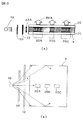
以下、図を参照して本発明を実施するための最良の形態について説明する。図1は本発明の一実施の形態を示す図であり、本発明によるファインダ内表示装置を備えた一眼レフカメラの概略構成を示す図である。カメラボディ1には、撮影レンズ2を備えるレンズ鏡筒3が交換可能に装着されている。4は記録媒体であるフィルムである。図1では銀塩フィルムを用いる一眼レフカメラを例に示したが、一眼レフ方式のデジタルカメラであれば記録媒体としてCCDやCMOS等の撮像素子が用いられる。
Hereinafter, the best mode for carrying out the present invention will be described with reference to the drawings. FIG. 1 is a diagram illustrating an embodiment of the present invention, and is a diagram illustrating a schematic configuration of a single-lens reflex camera including a viewfinder display device according to the present invention. A
撮影レンズ2とフィルム4との間には、被写体光をファインダ光学系へと反射するクイックリターンミラー5が配設されている。なお、図示していないが、フィルム4とクイックリターンミラー5との間にはシャッタが設けられている。フィルム4の感光材料面と光学的に共役な位置にはファインダスクリーン6が配置されており、被写体11からの被写体光はクイックリターンミラー5に反射されファインダスクリーン6上に結像する。ファインダスクリーン6上に結像された被写体像は、ペンタプリズム7および接眼レンズ8を介して観察することができる。なお、撮影の際にはクイックリターンミラー5が被写体光の光路上から光路外へと移動され、フィルム4上に被写体像が結像される。
A
また、カメラボディ1内には、ファインダ内表示素子9がファインダスクリーン6に隣接して配置されている。ファインダ内表示素子9の側方には、ファインダ内表示素子9を照明するための光源10が配置されている。この光源10にはLED等が用いられる。光源10とファインダ内表示素子9との間には、光源10からの光を直線偏光に変換する偏光変換素子である偏光板12が配設されている。
In the
光源10から出射された光は偏光板12で直線偏光に変換され、側面からファインダ内表示素子9内に入射する。後述するようにファインダ内表示素子9は屈折率型回折格子を用いた表示部を有する回折光学素子であり、ファインダ内表示素子9内に入射した光は、屈折率型回折格子によってペンタプリズム7方向へ回折される。ファインダ内表示素子9は駆動回路13により駆動制御されており、屈折率型回折格子で構成される表示部によりファインダ視野内に所定の情報を、例えば焦点検出エリア等を表示する。
The light emitted from the
ファインダ内表示素子9から出射された回折光は、ペンタプリズム7によって反射され、接眼レンズ8を介して撮影者に所定の情報として観察される。その結果、所定の情報が上述の被写体像に重ねてファインダ視野内に表示され、撮影者は被写体像と所定の情報とを同時に観察することが可能となる。
The diffracted light emitted from the in-
[ファインダ内表示素子9の説明]
次に、ファインダ内表示素子9について詳細に説明する。図2はファインダ内表示素子9の表示部と非表示部とを説明する図であり、ファインダ内表示素子9の断面を模式的に示したものである。ファインダ内表示素子9は一対のガラス基板20,21を有しており、各ガラス基板20,21の対向する面には透明電極22,23がそれぞれ形成されている。透明電極22,23は同一形状に形成されており、表示部の表示形態(文字や図形)に応じた形状を有している。透明電極22,23は上述した駆動回路13に接続されており、駆動回路13により透明電極22,23に印加される電圧が制御される。
[Description of
Next, the in-
透明電極22,23を備えたガラス基板20,21の間には液晶部材24が設けられており、ガラス基板20,21の間の周辺部分に配設されるシール材26により密封されている。液晶部材24には高分子分散型液晶が用いられ、透明電極22,23が設けられていない非表示部24Aは屈折率等方性を有する材料(高分子モノマー)と屈折率異方性を有する材料(液晶)とが未硬化の状態で混合された状態になっている。
A
一方、透明電極22,23によって挟まれた表示部24Bは液晶ホログラムとなっている部分であり、屈折率等方性領域層241と屈折率異方性領域層242とが、ファインダ内表示素子9の面に沿うように照明光の進行方向に交互に繰り返される縞状の多層構造を形成している。屈折率等方性領域層241は上述した高分子モノマーが硬化してポリマーとなっている領域であり、屈折率異方性領域層242では硬化した高分子ポリマー中に屈折率異方性材料である液晶が分散している。
On the other hand, the
図2に示すような多層構造を形成するには、レーザ光等を用いて干渉縞25を形成し、その干渉縞25が形成された領域にモノマーと液晶とが混合状態となった液晶基板を配設する。そのとき、非表示部24Aに干渉縞25が形成されないようにガラス基板20,21にマスクを形成する。モノマーは光重合により硬化するが、この際、干渉により光強度が強くなっている干渉縞明部251においてはモノマーが硬化したポリマーの層が形成される。逆に、光強度が弱い干渉縞暗部252における光重合速度は、干渉縞明部251における光重合速度よりも遅いため、光強度が強い領域(光重合速度が速い部分)にモノマーが引き寄せられる分だけ液晶の方の密度が高くなる。その結果、ポリマーからなる屈折率等方性領域層241と液晶密度の高いポリマーからなる屈折率異方性領域層242との層構造が、干渉縞と同一パターンで形成される。
In order to form a multilayer structure as shown in FIG. 2, an
上述したように、表示部24Bを挟むように設けられた透明電極22,23には駆動回路13(図1参照)によって電圧を印加することができるが、ポリマーからなる屈折率等方性領域層241は電圧が印加されているか否かによらず、等方的な屈折率を有している。一方、ポリマー中に液晶が分散している屈折率異方性領域層242は、電圧が印加されているか否かによって液晶の配向が変化し、それに伴って屈折率も変化する。
As described above, a voltage can be applied to the
透明電極22,23に電圧が印加されていない状態では、光源10の照明光のように表示部24Bの積層方向に向かって入射する光に対しては、液晶の屈折率とポリマーの屈折率とはブラッグ回折条件を満たすような互いに異なった屈折率値をとるようになっている。すなわち、電圧が印加されていない状態では、表示部24Bには屈折率の大きい層と屈折率の小さい層とが交互に並んだ屈折率型回折格子が形成される。このときの回折条件は、回折光がペンタプリズム7の方向に回折されるように設定されている。一方、電圧が印加された状態では、屈折率異方性領域層242内の液晶の配向が変化するとともに屈折率も変化し、液晶の屈折率がポリマーの屈折率と等しくなる。その結果、入射した光は回折されることなく表示部24Bを透過する。
In a state where no voltage is applied to the
図3は、ファインダ内表示素子9の透明電極への電圧のオン・オフと、表示のオン・オフとの関係を示す図である。図3(a)は印加電圧オフの状態を示し、図3(b)は印加電圧オンの状態を示す。なお、図3では、ファインダ内表示素子9に3つの表示部30A,30B,30Cが設けられており、各表示部30A〜30Cには上述した表示部24Bと同様に屈折率等方性領域層と屈折率異方性領域層との層構造が形成されている。
FIG. 3 is a diagram showing the relationship between the on / off state of the voltage applied to the transparent electrode of the in-
表示部30A〜30Cを挟む透明電極への電圧印加をオフすると、上述したように層構造部分が屈折率型回折格子として機能し、図3(a)のように照明光が図示上方(ペンタプリズム7方向)に回折されファインダ内表示素子9から出射される。その結果、撮影者は被写体像に表示部30A〜30Cの表示が重畳されて観察される。一方、透明電極への印加電圧をオフすると、図3(b)のように照明光は層構造部分で回折されず透過するので、接眼レンズ8(図1参照)へと導かれることがなく撮影者には被写体像のみが観察されることとなる。
When the voltage application to the transparent electrodes sandwiching the
このように、本実施の形態では、電圧が印加されていない状態において液晶の屈折率とポリマーの屈折率との間に屈折率差が生じて光を回折し、電圧印加時に液晶の配向が変化して液晶の屈折率とポリマーの屈折率とが等しくなるような構成とした。しかし、液晶の配向はこれに限られるものではなく、電圧が印加されていない状態において液晶の屈折率とポリマーの屈折率とが等しく、電圧印加時に液晶の配向が変化して液晶とポリマーとの間に屈折率差が生じて光を回折するような構成としても良い。 As described above, in this embodiment, in the state where no voltage is applied, a refractive index difference is generated between the refractive index of the liquid crystal and the refractive index of the polymer, and light is diffracted. Thus, the refractive index of the liquid crystal is equal to the refractive index of the polymer. However, the orientation of the liquid crystal is not limited to this, and the refractive index of the liquid crystal and the refractive index of the polymer are equal when no voltage is applied. A configuration in which a difference in refractive index occurs between them to diffract light may be adopted.
また、上述した実施の形態では、一対のガラス基板20,21の各々に同一形状の透明電極を形成したが、ガラス基板20,21の内の一方のガラス基板に透明電極を形成し、他方のガラス基板には基板面全体に一様に透明電極を形成するようにしても良い。このような構成のファインダ内表示素子でも、上述したファインダ内表示素子9と同様に回折光による表示をファインダ視野内に表示することができる。
In the above-described embodiment, the transparent electrode having the same shape is formed on each of the pair of
[偏光板12の説明]
次に、偏光板12の機能について図4を参照して説明する。図4は、ファインダ内表示素子9の非表示部24A(図2参照)の部分の液晶の状態を模式的に示したものであり、(a)は断面図、(b)は(a)のB−B断面図である。上述したように、非表示部24Aにおいては、非表示部24Aは屈折率等方性を有する材料(高分子モノマー)と屈折率異方性を有する材料(液晶)とが未硬化の状態で混合された状態になっており、41は液晶分子を表している。照明光は図示左側から入射する。
[Description of Polarizing Plate 12]
Next, the function of the
図4(a)の断面図のようの横方向から見ると、ガラス基板20,21に挟まれた液晶中の液晶分子41は寝た状態で層状になっている。なお、本実施の形態のファインダ内表示素子9では配向膜を使用していないので、厳密に層状になっておらず若干傾いているものもあるが、概略的には層状になっている。一方、図4(b)の断面図のようにファインダ内表示素子9を基板上方から見た場合には、液晶分子41の向き(液晶分子光軸方向)がランダムになっている。
When viewed from the side as shown in the sectional view of FIG. 4A, the
液晶分子41の向きが図4のような状態になっているファインダ内表示素子9の側面から、符合42Aで示すような直線偏光が入射した場合を考える。液晶分子41が寝ているため、直線偏光42Aのように基板に垂直な直線偏光に対しては、液晶の屈折率とモノマーの屈折率とが同じ値となる。そのため、直線偏光42Aは散乱されることなく非表示部24Aを透過する。一方、基板に平行な直線偏光42Bに対しては、液晶分子41の向きがランダムになっているために液晶の屈折率とモノマーの屈折率とが異なる値となり、非表示部24Aにおいて散乱が生じる。
Consider a case where linearly polarized light as indicated by
そのため、本実施の形態では、図1,3に示すように、基板に垂直な方向の偏光光を透過する偏光板12を光源10とファインダ内表示素子9との間に配設した。ファインダ内表示素子9には基板に垂直な直線偏光42Aのみが入射されるため、非表示部24Aにおいて照明光の散乱が生じない。その結果、図3(a)の表示部30A〜30Cと表示部周辺の非表示部24Aとのコントラストが向上する。
Therefore, in the present embodiment, as shown in FIGS. 1 and 3, a
また、直線偏光42Aは、図2の透明電極22,23に電圧を印加したときの液晶分子光軸方向と平行となるため、ファインダ内表示素子9から出射される回折光の回折効率を高めることができ、さらにコントラスト向上が図れる。なお、上述した実施の形態では、光源10と偏光板12とにより直線偏光成分の照明光を生成するようにしたが、このような照明光を生成するものであれば種々の照明手段を用いることができる。例えば、照明光を直線偏光42Aに変換する光学素子として、吸収型の偏光板12に代えて偏光選択性のホログラムを用いても良い。
Further, since the linearly
(変形例)
図5は本実施の形態の変形例を示す図であり、(a)はファインダ内表示素子9を側方から見た断面図であり、(b)は平面図である。変形例においては、偏光板12とファインダ内表示素子9との間にホログラム拡散素子50が配設されている。光源10にはLEDが用いられるが、LEDの場合、光が±30〜40度程度の角度で放射される。これに対して、ホログラム拡散素子50により光線の角度を大きくするように変更することにより、ファインダ内表示素子9内に入射した光を、ファインダ内表示素子9の側面において全反射させるようにすることができる。
(Modification)
FIG. 5 is a view showing a modification of the present embodiment, where (a) is a cross-sectional view of the in-
その結果、ファインダ内表示素子9の全域に照明光を均一に行きわたらせることが可能となり、表示部30A〜30Cによる表示を均一に行わせることができる。なお、ホログラム拡散素子50による拡散の度合い(角度変更の度合い)は、ファインダ内表示素子9の配置や寸法および全反射角度等を考慮することにより最適な値に設定される。また、照明光の放射角度を変えて拡散を行う素子として機能する放射角変換手段であれば、ホログラム拡散素子に限らない。
As a result, illumination light can be uniformly distributed over the entire area of the in-
以上では、本発明による回折型表示装置をカメラのファインダ内表示素子に用いた場合について説明したが、カメラ以外の各種光学装置に搭載しても良い。また、ファインダ内表示素子9は透明電極22,23の電圧印加をオンオフして表示のオンオフができる構成であったが、透明電極を有していない回折型表示装置にも本発明は適用できる。すなわち、図2のファインダ内表示素子9において透明電極22,23を省略した場合、屈折率異方性領域層242内の液晶分子の配向状態は透明電極22,23の印加電圧をオフとした場合と同じなので、常に回折機能が発生していることになる。そのため、光源10がオン状態である限り、表示部24Bの表示が行われることになる。また、光源10のオンオフにより表示部24Bのオンオフ制御を行うことも可能である。
The case where the diffractive display device according to the present invention is used as a display element in a viewfinder of a camera has been described above, but it may be mounted on various optical devices other than a camera. In addition, the
1:カメラボディ 6:ファインダスクリーン
9:ファインダ内表示素子 10:光源
12:偏光板 13:駆動回路
24:液晶部材 24A:非表示部
24B,30A〜30C:表示部 42A,42B:直線偏光
50:ホログラム拡散素子 241:屈折率等方性領域層
242:屈折率異方性領域層
1: Camera body 6: Finder screen 9: Display element in finder 10: Light source 12: Polarizing plate 13: Drive circuit 24:
50: Hologram diffusion element 241: Refractive index isotropic region layer
242: Refractive index anisotropic region layer
Claims (9)
直線偏光の照明光を前記回折光学素子の側面から入射する照明手段とを備え、
入射した照明光を前記回折表示部が設けられた基板面から出射することを特徴とする回折型表示装置。 Between the pair of substrates, a refractive index isotropic region composed of a refractive index isotropic material and a refractive index anisotropic region including a liquid crystal with refractive index anisotropy are alternately arranged in a direction along the substrate surface. a diffraction display portion and, disposed around the diffraction display portion, and a diffractive optical element and a non-display portion formed with a mixed material of the liquid crystal and the refractive index isotropic material,
Illuminating means for entering linearly polarized illumination light from the side surface of the diffractive optical element,
A diffractive display device that emits incident illumination light from a substrate surface provided with the diffractive display portion.
前記照明手段は、自然偏光または部分偏光の状態を有する無偏光を出射する光源と、前記光源から出射された光を前記液晶基板に垂直な方向の直線偏光に変換する偏光変換素子とを備えることを特徴とする回折型表示装置。 The diffractive display device according to claim 1,
The illumination unit includes a light source that emits non-polarized light having a state of natural polarization or partial polarization, and a polarization conversion element that converts light emitted from the light source into linearly polarized light in a direction perpendicular to the liquid crystal substrate. A diffractive display device characterized by the above.
前記屈折率等方性領域は、高分子モノマーが硬化してポリマーとなっている領域であり、 The refractive index isotropic region is a region where a polymer monomer is cured to become a polymer,
前記屈折率異方性領域は、高分子ポリマー中に液晶が分散していることを特徴とする回折型表示装置。 In the refractive index anisotropic region, a liquid crystal is dispersed in a polymer polymer.
前記光源は、LEDであることを特徴とする回折型表示装置。 The diffractive display device, wherein the light source is an LED.
前記偏光変換素子として、偏光選択性を有するホログラム素子を用いたことを特徴とする回折型表示装置。 In the diffraction type display apparatus as described in any one of Claims 1-4 ,
A diffractive display device using a hologram element having polarization selectivity as the polarization conversion element.
前記照明手段と前記液晶基板の側面との間に配設され、前記照明光の前記液晶基板の面に沿った放射角を変換する放射角変換手段を設けたことを特徴とする回折型表示装置。 In the diffraction type display apparatus as described in any one of Claims 1-5 ,
A diffractive display device provided with a radiation angle converting means disposed between the illuminating means and a side surface of the liquid crystal substrate and converting a radiation angle of the illumination light along the surface of the liquid crystal substrate. .
前記放射角変換手段は、前記回折光学素子に入射した前記照明光が前記回折光学素子の側面界面において全反射されるように放射角を変換することを特徴とする回折型表示装置。 The diffractive display device according to claim 6 ,
The diffractive display device according to claim 1, wherein the radiation angle converting means converts the radiation angle so that the illumination light incident on the diffractive optical element is totally reflected at a side interface of the diffractive optical element.
前記回折光学素子をカメラのファインダスクリーンの近傍に配置し、前記回折表示部で回折された照明光をファインダ内表示に用いることを特徴とするファインダ内表示装置。 The diffractive display device according to any one of claims 1 to 7 ,
An in-finder display device, wherein the diffractive optical element is disposed in the vicinity of a finder screen of a camera, and illumination light diffracted by the diffraction display unit is used for in-finder display.
前記ファインダ内表示装置は、前記ファインダスクリーンの像に前記回折表示部で回折された照明光による像を重畳して表示することを特徴とするカメラ。 The in-finder display device superimposes and displays an image of illumination light diffracted by the diffraction display unit on an image of the finder screen.
Priority Applications (5)
| Application Number | Priority Date | Filing Date | Title |
|---|---|---|---|
| JP2005150027A JP4586630B2 (en) | 2005-05-23 | 2005-05-23 | Diffraction type display device and display device in viewfinder of camera |
| EP06114124A EP1726986B1 (en) | 2005-05-23 | 2006-05-17 | Diffractive display device and corresponding display method |
| DE602006015566T DE602006015566D1 (en) | 2005-05-23 | 2006-05-17 | Diffractive display device and corresponding display method |
| US11/436,611 US7542669B2 (en) | 2005-05-23 | 2006-05-19 | Diffraction display device and viewfinder display device |
| CN2006100848552A CN1892338B (en) | 2005-05-23 | 2006-05-23 | Diffraction display device and viewfinder display device |
Applications Claiming Priority (1)
| Application Number | Priority Date | Filing Date | Title |
|---|---|---|---|
| JP2005150027A JP4586630B2 (en) | 2005-05-23 | 2005-05-23 | Diffraction type display device and display device in viewfinder of camera |
Publications (3)
| Publication Number | Publication Date |
|---|---|
| JP2006330103A JP2006330103A (en) | 2006-12-07 |
| JP2006330103A5 JP2006330103A5 (en) | 2008-06-05 |
| JP4586630B2 true JP4586630B2 (en) | 2010-11-24 |
Family
ID=36763692
Family Applications (1)
| Application Number | Title | Priority Date | Filing Date |
|---|---|---|---|
| JP2005150027A Expired - Fee Related JP4586630B2 (en) | 2005-05-23 | 2005-05-23 | Diffraction type display device and display device in viewfinder of camera |
Country Status (5)
| Country | Link |
|---|---|
| US (1) | US7542669B2 (en) |
| EP (1) | EP1726986B1 (en) |
| JP (1) | JP4586630B2 (en) |
| CN (1) | CN1892338B (en) |
| DE (1) | DE602006015566D1 (en) |
Families Citing this family (15)
| Publication number | Priority date | Publication date | Assignee | Title |
|---|---|---|---|---|
| JP5309468B2 (en) | 2006-05-31 | 2013-10-09 | 株式会社ニコン | Liquid crystal display element, display device, observation device, and camera |
| JP2008015125A (en) * | 2006-07-05 | 2008-01-24 | Nikon Corp | Display element, display device and camera |
| JP5218061B2 (en) * | 2006-10-06 | 2013-06-26 | 株式会社ニコン | Diffraction type display device, finder device and camera |
| US8436976B2 (en) | 2007-02-26 | 2013-05-07 | Nikon Corporation | Display device, finder device and camera |
| CN101878446B (en) * | 2007-11-30 | 2013-03-06 | 夏普株式会社 | Liquid crystal display |
| JP2011059582A (en) * | 2009-09-14 | 2011-03-24 | Sony Corp | Imaging device |
| GB201015417D0 (en) * | 2010-09-15 | 2010-10-27 | Lomox Ltd | Organic light emitting diode devices |
| US9523609B2 (en) * | 2013-04-10 | 2016-12-20 | Bae Systems Plc | Spectral imaging |
| US10324245B2 (en) | 2014-07-29 | 2019-06-18 | Samsung Electronics Co., Ltd. | Backlight unit for holographic display |
| US11126060B2 (en) | 2017-10-02 | 2021-09-21 | Liqxtal Technology Inc. | Tunable light projector |
| US20190101791A1 (en) * | 2017-10-02 | 2019-04-04 | Liqxtal Technology Inc. | Optical sensing device and structured light projector |
| US10802382B2 (en) * | 2018-07-24 | 2020-10-13 | Qualcomm Incorporated | Adjustable light projector for flood illumination and active depth sensing |
| KR20200042582A (en) * | 2018-10-15 | 2020-04-24 | 삼성디스플레이 주식회사 | Display device and fabricating method thereof |
| KR20210006709A (en) * | 2019-07-09 | 2021-01-19 | 현대자동차주식회사 | Transparency variable glass and apparatus of controlling transparency of the same |
| CN113272726B (en) * | 2019-10-24 | 2022-08-23 | 京东方科技集团股份有限公司 | Display panel, display device and display panel manufacturing method |
Citations (5)
| Publication number | Priority date | Publication date | Assignee | Title |
|---|---|---|---|---|
| JP2002023107A (en) * | 2000-07-05 | 2002-01-23 | Sony Corp | Picture display element and picture display device |
| JP2002122906A (en) * | 2000-10-17 | 2002-04-26 | Olympus Optical Co Ltd | Display device within finder |
| JP2002221621A (en) * | 2001-01-26 | 2002-08-09 | Sony Corp | Polarization selective hologram optical element, image display element and image display device |
| JP2003532918A (en) * | 2000-05-04 | 2003-11-05 | コーニンクレッカ フィリップス エレクトロニクス エヌ ヴィ | Illumination unit for device with reflective multi-color liquid crystal display |
| JP2004191415A (en) * | 2002-12-06 | 2004-07-08 | Nikon Corp | Holographic optical element, in-finder display device of camera, and camera |
Family Cites Families (3)
| Publication number | Priority date | Publication date | Assignee | Title |
|---|---|---|---|---|
| JPH09152553A (en) | 1995-11-30 | 1997-06-10 | Mitsubishi Electric Corp | Light source device and projection type display device using same |
| WO2000079338A1 (en) * | 1999-06-23 | 2000-12-28 | Citizen Watch Co., Ltd. | Liquid crystal display |
| EP1420275B1 (en) * | 2001-08-24 | 2008-10-08 | Asahi Glass Company, Limited | Isolator and optical attenuator |
-
2005
- 2005-05-23 JP JP2005150027A patent/JP4586630B2/en not_active Expired - Fee Related
-
2006
- 2006-05-17 DE DE602006015566T patent/DE602006015566D1/en active Active
- 2006-05-17 EP EP06114124A patent/EP1726986B1/en not_active Expired - Fee Related
- 2006-05-19 US US11/436,611 patent/US7542669B2/en not_active Expired - Fee Related
- 2006-05-23 CN CN2006100848552A patent/CN1892338B/en not_active Expired - Fee Related
Patent Citations (5)
| Publication number | Priority date | Publication date | Assignee | Title |
|---|---|---|---|---|
| JP2003532918A (en) * | 2000-05-04 | 2003-11-05 | コーニンクレッカ フィリップス エレクトロニクス エヌ ヴィ | Illumination unit for device with reflective multi-color liquid crystal display |
| JP2002023107A (en) * | 2000-07-05 | 2002-01-23 | Sony Corp | Picture display element and picture display device |
| JP2002122906A (en) * | 2000-10-17 | 2002-04-26 | Olympus Optical Co Ltd | Display device within finder |
| JP2002221621A (en) * | 2001-01-26 | 2002-08-09 | Sony Corp | Polarization selective hologram optical element, image display element and image display device |
| JP2004191415A (en) * | 2002-12-06 | 2004-07-08 | Nikon Corp | Holographic optical element, in-finder display device of camera, and camera |
Also Published As
| Publication number | Publication date |
|---|---|
| JP2006330103A (en) | 2006-12-07 |
| EP1726986A1 (en) | 2006-11-29 |
| US20060263079A1 (en) | 2006-11-23 |
| US7542669B2 (en) | 2009-06-02 |
| DE602006015566D1 (en) | 2010-09-02 |
| CN1892338A (en) | 2007-01-10 |
| EP1726986B1 (en) | 2010-07-21 |
| CN1892338B (en) | 2011-11-09 |
Similar Documents
| Publication | Publication Date | Title |
|---|---|---|
| JP4586630B2 (en) | Diffraction type display device and display device in viewfinder of camera | |
| US4856869A (en) | Display element and observation apparatus having the same | |
| JP4631308B2 (en) | Image display device | |
| US8345189B2 (en) | Diffractive display device, finder device and camera | |
| US7702237B2 (en) | Observation device, camera and observation method | |
| US6975810B2 (en) | Focal point detection device and camera | |
| JP2007047769A (en) | Display device | |
| JP4788301B2 (en) | Display device and camera | |
| US7652710B2 (en) | Camera with photometric function and optical element for camera | |
| JP5218392B2 (en) | Display device, finder device and camera | |
| JP2006154506A (en) | Optical element and focus detector | |
| JP2007017695A (en) | Display device and camera | |
| JP5169420B2 (en) | Lighting device, display device, finder device, and camera | |
| JP2007017788A (en) | Display device | |
| JP4544207B2 (en) | Display device and camera | |
| JP2007047578A (en) | Diffraction optical apparatus and camera | |
| JP5169417B2 (en) | Lighting device, display device, finder device, and camera | |
| JP2008227868A (en) | Display device, finder device, and camera | |
| JP3916244B2 (en) | Reflective liquid crystal display device using hologram | |
| JP2008203325A (en) | Display device, finder device, camera, and method of manufacturing display device | |
| JPS6234141A (en) | In-finder display device | |
| JP2004294725A (en) | Focus detecting device | |
| JPS63218920A (en) | Optical modulating element | |
| JP2006010834A (en) | Optical modulation element, display device, display system in finder of camera, and diffraction type optical apparatus | |
| JPS63218919A (en) | Observing device |
Legal Events
| Date | Code | Title | Description |
|---|---|---|---|
| A621 | Written request for application examination |
Free format text: JAPANESE INTERMEDIATE CODE: A621 Effective date: 20080403 |
|
| A521 | Request for written amendment filed |
Free format text: JAPANESE INTERMEDIATE CODE: A523 Effective date: 20080417 |
|
| A977 | Report on retrieval |
Free format text: JAPANESE INTERMEDIATE CODE: A971007 Effective date: 20100730 |
|
| TRDD | Decision of grant or rejection written | ||
| A01 | Written decision to grant a patent or to grant a registration (utility model) |
Free format text: JAPANESE INTERMEDIATE CODE: A01 Effective date: 20100810 |
|
| A01 | Written decision to grant a patent or to grant a registration (utility model) |
Free format text: JAPANESE INTERMEDIATE CODE: A01 |
|
| A61 | First payment of annual fees (during grant procedure) |
Free format text: JAPANESE INTERMEDIATE CODE: A61 Effective date: 20100823 |
|
| R150 | Certificate of patent or registration of utility model |
Ref document number: 4586630 Country of ref document: JP Free format text: JAPANESE INTERMEDIATE CODE: R150 Free format text: JAPANESE INTERMEDIATE CODE: R150 |
|
| FPAY | Renewal fee payment (event date is renewal date of database) |
Free format text: PAYMENT UNTIL: 20130917 Year of fee payment: 3 |
|
| FPAY | Renewal fee payment (event date is renewal date of database) |
Free format text: PAYMENT UNTIL: 20130917 Year of fee payment: 3 |
|
| R250 | Receipt of annual fees |
Free format text: JAPANESE INTERMEDIATE CODE: R250 |
|
| R250 | Receipt of annual fees |
Free format text: JAPANESE INTERMEDIATE CODE: R250 |
|
| R250 | Receipt of annual fees |
Free format text: JAPANESE INTERMEDIATE CODE: R250 |
|
| R250 | Receipt of annual fees |
Free format text: JAPANESE INTERMEDIATE CODE: R250 |
|
| R250 | Receipt of annual fees |
Free format text: JAPANESE INTERMEDIATE CODE: R250 |
|
| R250 | Receipt of annual fees |
Free format text: JAPANESE INTERMEDIATE CODE: R250 |
|
| R250 | Receipt of annual fees |
Free format text: JAPANESE INTERMEDIATE CODE: R250 |
|
| R250 | Receipt of annual fees |
Free format text: JAPANESE INTERMEDIATE CODE: R250 |
|
| LAPS | Cancellation because of no payment of annual fees |