JP4585899B2 - Multi-layer disc carrier information recording / reproducing apparatus - Google Patents
Multi-layer disc carrier information recording / reproducing apparatus Download PDFInfo
- Publication number
- JP4585899B2 JP4585899B2 JP2005089563A JP2005089563A JP4585899B2 JP 4585899 B2 JP4585899 B2 JP 4585899B2 JP 2005089563 A JP2005089563 A JP 2005089563A JP 2005089563 A JP2005089563 A JP 2005089563A JP 4585899 B2 JP4585899 B2 JP 4585899B2
- Authority
- JP
- Japan
- Prior art keywords
- recording
- light
- groove
- signal
- control
- Prior art date
- Legal status (The legal status is an assumption and is not a legal conclusion. Google has not performed a legal analysis and makes no representation as to the accuracy of the status listed.)
- Expired - Fee Related
Links
Images


Landscapes
- Optical Recording Or Reproduction (AREA)
- Optical Head (AREA)
Description
本発明は多層ディスク情報記録担体に信号記録、および信号読み出しを行う装置の分野に関わる物である。 The present invention relates to the field of apparatus for recording and reading signals on a multilayer disc information record carrier.
近年情報量の大量化に伴って光情報記録担体(ディスク担体)の高容量化が強く求められている。 In recent years, there has been a strong demand for an increase in capacity of an optical information record carrier (disc carrier) as the amount of information increases.
光ディスク上の記録密度は、
(NA/λ)2
λ:記録再生光源波長
NA:対物レンズ開口数
に比例するから、近年λとして405nm GaNレーザ、対物レンズNAは0.85を用いることで、5インチ直径ディスクでDVDディスクの約6倍程度の記録容量25GByteを達成しようとしている。
The recording density on the optical disc is
(NA / λ) 2
λ: Recording / reproducing light source wavelength
NA: Since it is proportional to the numerical aperture of the objective lens, in recent years, a 405 nm GaN laser is used as λ, and the objective lens NA is 0.85. Yes.
しかしこの様に対物レンズNAを可能な限り上げ、又記録再生光源波長を可能な限り短くし記録容量を上昇させる方法はほぼ限界に達してきた。 However, the method of increasing the recording capacity by increasing the objective lens NA as much as possible and shortening the recording / reproducing light source wavelength as much as possible has almost reached the limit.
もし光源波長が405nmより短くなればディスク担体樹脂基板として、従来用いられてきたポリカーボネイト基板の光透過率が急速に低減化する。 If the light source wavelength is shorter than 405 nm, the light transmittance of a polycarbonate substrate conventionally used as a disk carrier resin substrate is rapidly reduced.
又、光源波長が400nmより短くなると樹脂基板は透過率が低下すると共に、光源の長時間照射に対しては組成分解が起こり、更に光透過率が下がるとの問題が発生する。 Further, when the wavelength of the light source is shorter than 400 nm, the transmittance of the resin substrate is reduced, and compositional decomposition occurs when the light source is irradiated for a long time, and the light transmittance is further lowered.
一方、対物レンズのNAはこれ以上増加させた場合、更に対物レンズとディスク担体間距離(WD)が小さくなり記録膜上に製作される保護層膜もWDの制限や、ディスク担体のチルトマージンの観点から100μm以下になってしまう。従ってWDが小さくなるから 更に対物レンズはディスク担体と衝突しやすくなり、かつ保護層も100μm以下になるからディスク保護層面上の汚れが信号面からごく近くなり、少しのディスク保護層面上汚れがディスク再生信号の劣化になってしまう。 On the other hand, when the NA of the objective lens is further increased, the distance (WD) between the objective lens and the disk carrier is further reduced, so that the protective layer film produced on the recording film also has a WD limitation and a tilt margin of the disk carrier. From the viewpoint, it becomes 100 μm or less. Therefore, since the WD becomes smaller, the objective lens is more likely to collide with the disk carrier, and the protective layer is also less than 100 μm, so that the dirt on the disk protective layer is very close to the signal surface, and a little dirt on the disk protective layer is found on the disk. The playback signal will deteriorate.
この様に今までの様にλを短くし、対物レンズNAを更に大きくして高容量化を達成してゆくことは、種々の問題が発生しこれを克服するには相当な技術開発を行う必要がある。 As described above, shortening λ and further increasing the objective lens NA to achieve higher capacity will cause various problems, and considerable technological development will be performed to overcome this problem. There is a need.
従って光ディスクの更なる高容量化には記録層を多数に積層する方法が比較的問題が少なく、今後この方式が主流に成ると考えられる。 Therefore, the method of laminating a large number of recording layers has relatively few problems for further increasing the capacity of the optical disk, and this method is considered to become the mainstream in the future.
この為図12で示されるような多層ディスク担体が発表されてきた。この多層ディスク担体は最下層に片面に溝面と非溝面からなる制御溝53を有する担体基板56があり、その上に分離層52、その上に記録膜51の繰り返しから成る多層記録膜を有している。又、従来の光ディスク担体製造技術を用いて、転写によりこの分離層を形成するときは、分離層52上に担体基板と同様の制御溝が作成されて行く。この後記録膜51を形成するから各層の記録膜51には凹凸状の制御溝53が形成されている。
For this reason, a multilayer disk carrier as shown in FIG. 12 has been announced. This multi-layer disc carrier has a
この様な構造で記録膜を多層化し記録容量を向上しようとしている。 With such a structure, the recording film is multilayered to improve the recording capacity.
記録膜51としては従来の一光子光吸収による発熱で膜の相転移や、変形を利用し信号を記録する半透明一光子吸収記録膜、あるいは従来の一光子光吸収記録とは全く原理の異なる多光子吸収を利用し信号を記録する完全透明多光子記録膜が用いられる。前者の半透明記録膜は光を吸収するため記録膜の総数が4−5層以上になると光の減衰が大きくなりこれより深い層の記録膜には記録できなくなり記録容量の制限が起こる。
The
この問題を克服するため近年完全な透明膜を用いる多光子吸収記録が注目を浴びている(例えば、特許文献1参照)。多光子吸収記録の場合は、光集光点3近傍の光電界が極めて強いところの電子が励起され光吸収反応が起こるが、一方光集光点3以外では光吸収が起こらない。従って多光子吸収記録材は従来の半透明記録膜のように記録膜51を単に通過することだけでは、光が減衰しない完全透明材料であるから、非常に多くの記録膜を重ねることが出来、高容量化には遙かに有利である。
In order to overcome this problem, multiphoton absorption recording using a complete transparent film has recently attracted attention (see, for example, Patent Document 1). In the case of multiphoton absorption recording, electrons where the optical electric field in the vicinity of the
この様に多層化に必要な技術は一つ大きな前進を見せている。 In this way, the technology required for multi-layering is one major advance.
しかしディスク担体の多層化について更に大きな問題点がある。それは光集光点3を決められた制御溝53の上を各記録膜51の上で如何に正確に掃引することが出来るかの問題がある。この問題を多層ディスク担体記録再生装置側で簡単に解決するためには図12に示されるごとく従来の光ディスク記録担体と同様に各記録膜51に凹凸の制御溝を付け、これに記録再生集光点3bを追従させる方法が考えられる。この方法は確かに従来の積み重ねであるから容易に問題解決出来そうであるが多層化には大きな問題となる。
However, there is an even greater problem with multi-layer disk carriers. The problem is how accurately the
なぜなら前述したごとく各記録膜51に制御溝53を形成するためには分離層52を塗布、硬化する時に分離層52の表面にスタンパーを押しつけ、前記分離層がUV樹脂で形成されるならスタンパーの反対側(通常は担体基板56側)からUV光を照射し硬化させ、その後スタンパーを剥離してゆく必要がある。
Because, as described above, in order to form the
従って記録層を構成するたびごとにスタンパーによる加圧、剥離操作が発生するから各分離層内に大きなひずみ力が残りこの転写操作を10−30回繰り返した場合、ディスクに発生する残留応力は、きわめて大きくなる。 Therefore, each time the recording layer is constructed, a pressing and peeling operation by a stamper occurs, so that a large strain force remains in each separation layer, and when this transfer operation is repeated 10-30 times, the residual stress generated in the disc is: Become very large.
この様に作られた多層ディスク担体の面振れ、もしくは高温高湿状態で本ディスク担体の面振れ量は、単純に考えた場合でも一層ディスクの面振れ量の2乗平均で加算されて行くから30層から成る多層ディスク担体の場合一層から成るディスク担体に比較し√30=5.5倍程度の面振れが発生し非常に質の悪いディスクが制作されることになる。 The surface runout of the multi-layer disc carrier made in this way, or the surface runout amount of the present disc carrier in a high temperature and high humidity state is added by the square average of the disc runout amount even if simply considered. In the case of a multi-layer disc carrier consisting of 30 layers, a surface runout of √30 = 5.5 times occurs compared to a disc carrier consisting of one layer, and a very poor quality disc is produced.
又、この様に記録各層に制御溝53を入れることになれば多回数の転写工程が入るから生産性が悪くなり、多層ディスク担体のコストアップに成る。
この問題を解決するため図13に示されるごとく制御溝53を担体基板56の面上にだけ従来の光ディスクの成形技術を用い作成し、それ以外の記録膜51には制御溝53を付けないで多層ディスク担体の製造工程を単純化することが考えられる。
In order to solve this problem, as shown in FIG. 13, the
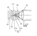
さてこの様な多層ディスク担体に信号を書き込む為の記録再生装置として従来考えられて来た光学系を図13に示す。 FIG. 13 shows an optical system conventionally considered as a recording / reproducing apparatus for writing a signal on such a multilayer disk carrier.
図中、半導体レーザ1aが担体基板上の制御溝53を照射するための制御集光点3aを構成する光学系となっている。一方記録再生集光点3bは発振波長650nmの半導体レーザ1bから発光された光を対物レンズ10によって集光することにより構成している。
In the figure, the semiconductor laser 1a is an optical system constituting a
記録膜51は多数有るがどの層に記録するかは対物レンズ10を11方向に移動することで記録再生集光点3bの位置を移動させ記録させるべき記録膜51が決定される。この対物レンズ10を11方向に移動させると制御溝53上を正確に照射すべき制御集光点3aの位置も11方向に移動してしまう。これを補正するためにコリメータレンズ2a及び半導体レーザ1aを12方向に移動させこの制御集光点3aが絶えず制御溝53上に正確に集光する様に制御する。しかしこの様な光学構成で記録再生集光点3bと制御集光点3aを光軸13上で絶えず安定に一致させるのは非常に困難である。例えば半導体レーザ1a、1bの光線中心軸は熱と共に0.1度程度は移動するし、対物レンズ10を記録膜51を切り替えるため11方向に移動させる、又コリメータレンズ2aもしくは半導体レーザ1aを12方向に移動させると、これらと直角方向の成分もどうしても混入するから、制御集光点3aと記録再生集光点3bを絶えず光軸13上に配置することは困難である。
Although there are
上記課題を解決するために、第1の本発明は、
片面に溝面と非溝面によって形成される制御溝を有する担体基板、並びに、前記担体基板の制御溝上に形成された分離層、及び前記分離層上に形成された記録膜の繰り返しを有する多層記録膜を備え、
信号の記録が行われた前記記録膜は、記録済み面と未記録面から形成される信号溝を有し、
前記多層記録膜を通過し、前記担体基板に到達した入射光に対する、前記溝面からの反射光は、前記非溝面からの反射光とは位相が異なり、
前記多層記録膜の一部を通過し、前記記録膜に到達した入射光に対する、前記記録済み面からの反射光は、前記未記録面からの反射光とは位相が異なる、多層ディスク担体を記録再生する多層ディスク担体情報記録再生装置であって、
前記多層ディスク担体に、記録及び再生のうち少なくとも一方を行うための光を照射する1つの光源と、
前記多層ディスク担体と前記光源の間に設置され、前記信号の記録及び再生のうち少なくとも一方を行うための集光点である記録再生集光点を形成する対物レンズと、
前記記録再生集光点を形成する光のうち、前記記録再生集光点が形成されている前記記録膜を透過した記録膜透過光の、前記記録再生集光点が形成されている記録膜に隣接する前記制御溝若しくは前記信号溝からの反射光を用いて、前記記録再生集光点の前記記録膜上における左右方向に対する位置の制御を行う制御手段とを備えた、多層ディスク担体情報記録再生装置である。
In order to solve the above problems, the first aspect of the present invention provides:
A carrier substrate having a control groove formed by a groove surface and a non-groove surface on one side, a separation layer formed on the control groove of the carrier substrate, and a multilayer having a repetition of a recording film formed on the separation layer With a recording film,
The recording film on which the signal is recorded has a signal groove formed from a recorded surface and an unrecorded surface,
The incident light that has passed through the multilayer recording film and has reached the carrier substrate, the reflected light from the groove surface is different in phase from the reflected light from the non-groove surface,
The reflected light from the recorded surface with respect to the incident light that has passed through a part of the multilayer recording film and reached the recording film has a phase different from that of the reflected light from the unrecorded surface. A multilayer disk carrier information recording / reproducing apparatus for reproducing,
One light source for irradiating the multilayer disc carrier with light for at least one of recording and reproduction;
An objective lens that is installed between the multilayer disc carrier and the light source and forms a recording / reproducing condensing point that is a condensing point for performing at least one of recording and reproduction of the signal;
Of the light that forms the recording / reproducing condensing point, the recording film transmitted light that has passed through the recording film on which the recording / reproducing condensing point is formed is applied to the recording film on which the recording / reproducing condensing point is formed. Multi-layer disc carrier information recording / reproduction comprising control means for controlling the position of the recording / reproducing condensing point in the left-right direction on the recording film using reflected light from the adjacent control groove or signal groove Device.
又、第2の本発明は、
前記反射光を受光する2分割光検出器と、
前記2分割光検出器の前に配置された、光透過を阻止する、複数の直線状の部分から成る光透過阻止格子とを備え、
前記制御手段は、前記2分割光検出器の2つの光検出器のそれぞれの出力の差動信号から得た制御信号で、前記記録再生集光点が前記制御溝若しくは前記信号溝の上を移動するように制御を行う、第1の本発明の多層ディスク担体情報記録再生装置である。
The second aspect of the present invention is
A two-part photodetector for receiving the reflected light;
A light transmission blocking grating composed of a plurality of linear portions disposed in front of the two-part photodetector for blocking light transmission;
It said control means moves said control signal obtained from the differential signal of each of the outputs of the two photodetectors of the two-divided photodetector, wherein the recording and reproducing condensing point is over the control groove or said signal groove The multilayer disc carrier information recording / reproducing apparatus according to the first aspect of the present invention performs control as described above.
又、第3の本発明は、
前記光透過阻止格子は、前記反射光に対し透明である平板の一面に作成されており、前記一面と前記2分割光検出器面とが密着している、第2の本発明の多層ディスク担体情報記録再生装置である。
The third aspect of the present invention
The light transmission blocking grating, said being created on one side of the plate is transparent to the reflected light, said one surface and said two-division photodetector surfaces are in close contact, multi-layer disk carrier of the second of the present invention An information recording / reproducing apparatus.
又、第4の本発明は、
前記制御溝若しくは前記信号溝からの前記反射光が前記対物レンズを通過した後結像される位置に、前記2分割光検出器面と前記平板との密着面が配置されている、第3の本発明の多層ディスク担体情報記録再生装置である。
The fourth aspect of the present invention is
The control Mizowaka properly in position where the reflected light from the signal grooves are imaged after passing through the objective lens, the contact surface between the plate and the two-divided photodetector surfaces are arranged, the 3 is a multi-layer disc carrier information recording / reproducing apparatus according to the present invention.
又、第5の本発明は、
前記平板は、中心部材として設けられた液晶と、前記液晶を挟むように設けられた2つの透明電極とを備え、
前記制御手段は、前記透明電極の電極間に電位を与えることによって、前記制御信号の誤差を低減する、第4の本発明の多層ディスク担体情報記録再生装置である。
The fifth aspect of the present invention is
The flat plate includes a liquid crystal provided as a central member, and two transparent electrodes provided so as to sandwich the liquid crystal,
The control means is the multilayer disc carrier information recording / reproducing apparatus according to the fourth aspect of the present invention, wherein an error is applied to the control signal by applying a potential between the transparent electrodes.
又、第6の本発明は、
前記反射光が、前記対物レンズを通過後に結像する位置に設置された、格子形状を有する光検出器を備え、
前記制御手段は、前記格子形状を有する光検出器の差動信号で、前記記録再生集光点が前記制御溝若しくは前記信号溝の上を移動するように制御を行う、第1の本発明の多層ディスク担体情報記録再生装置である。
The sixth aspect of the present invention
A light detector having a lattice shape, installed at a position where the reflected light forms an image after passing through the objective lens;
The control means, a differential signal of the photodetector having the lattice shape, the recording reproducing condensing point is the control Mizowaka properly performs control to move the top of the signal grooves, first the It is the multilayer disk carrier information recording / reproducing apparatus of the invention.
又、第7の本発明は、
前記格子形状を有する光検出器は、前記結像である干渉模様の平行方向と平行になるように長手方向が配置された複数の棒状の光検出器である、第6の本発明の多層ディスク担体情報記録再生装置である。
The seventh aspect of the present invention
Photodetector having the lattice shape, the a photodetector of the plurality of rod-like longitudinal direction is arranged parallel to the parallel direction of the interference pattern is imaged, the sixth multi-layer disc of the present invention This is a carrier information recording / reproducing apparatus.
例えば、本発明は、多層ディスク情報記録担体上に情報を記録再生する装置において、前記多層ディスク情報記録担体は同一平面上に無い担体基板56、記録膜51、分離層52から成り、かつ前記担体基板平面は記録膜、分離層を通過し到達した入射光に対し弱い反射光を与えると共に反射光に対し位相差を与える溝(制御溝53)が有り、一方前記記録膜も前記入射光に対し弱い反射光を与えると共に記録済み部分からは前記記録膜反射光とは位相の異なる弱い反射を与える組成から成るもので構成されており、一方前記記録再生装置の対物レンズ10からの出射光が一つ以上の集光点を形成しこの内の一つの集光点(記録再生集光点3b)は前記記録膜上に置かれ情報記録もしくは情報再生を行うと共に、集光点による記録膜からの透過光が隣接する記録層に記録された信号を制御溝として、もしくは隣接する担体基板平面の制御溝からの反射信号を検出することにより前記記録再生集光点を制御することを特徴とする情報記録再生装置である。
For example, the present invention relates to an apparatus for recording and reproducing information on a multilayer disc information record carrier, wherein the multilayer disc information record carrier comprises a
本発明を用いることにより多層構造情報記録担体の各記録層には制御溝を作成する必要がなく多層情報記録担体の製造方法が簡単になり低コスト化と多層情報記録担体の高精度かが達成される。一方この様な情報記録担体を用いても対物レンズからの出力光量を損失なく、且つ安定に制御溝信号を検出することが可能となる。 By using the present invention, it is not necessary to create a control groove in each recording layer of the multilayer structure information record carrier, the production method of the multilayer information record carrier is simplified, and low cost and high accuracy of the multilayer information record carrier are achieved. Is done. On the other hand, even when such an information record carrier is used, the control groove signal can be detected stably without losing the amount of light output from the objective lens.
本発明は図13の従来のごとく個別の2ヶの半導体レーザを用い記録再生集光点3bと制御集光点3aを作り出すのではなく、あくまでも一つのレーザからの出射光をうまく分離し、いずれかの記録膜51に制御溝53、もしくは記録済みピット信号の記録溝から記録再生集光点3bの位置を制御し多層ディスク情報記録担体に安定に信号記録を行なうために成されたものである。
The present invention does not create the recording / reproducing
本発明では記録再生集光点3bを制御するために従来行われてきた各記録膜上に前記記録再生集光点の位置制御用の制御溝53を作らず、制御溝は最下層、もしくは最上層の担体基板、もしくは保護層のみに作成する。
In the present invention, the
従って、多層ディスク担体として非常に製作しやすく安価であり、ディスク担体歪みのないものが製作できる。本発明はこの様な多層ディスク担体の各記録膜51上に正確な位置に信号を記録するためになされた。
Therefore, it is very easy to manufacture as a multi-layer disk carrier, and it is inexpensive and a disk carrier without distortion can be manufactured. The present invention has been made to record a signal at an accurate position on each
又、本発明を用いることで制御集光点を作らず対物レンズ10から出射された光束で記録再生集光点3bだけを形成し上記制御溝付担体基板56に隣接する記録膜51a上に情報記録を行いこの隣接する記録膜51aの全面で情報記録が完了した時、保護層50方向に対物レンズ10を移動させることで次の記録膜51bに記録再生集光点3bを移動させて、この記録膜51b上に記録を行ってゆく。同じ方法を繰り返すことで多層ディスク担体上の記録膜に次々と前記制御溝と同一上の位置に記録を行う為の記録再生集光点を制御する溝制御信号を得るための安価な光学系を提供するために成されたものである。
Further, the present invention forms a only the reproducing converging
(実施の形態1)
本発明の実施例の一つを図1、図2に示し詳細に説明を加える。
(Embodiment 1)
One embodiment of the present invention is shown in FIGS. 1 and 2 and will be described in detail.
まず最初に図1に示す担体基板56に隣接した記録膜51aに情報を記録するときの説明を行う。
First, a description will be given of recording information on the
この時、記録膜51a上に形成された記録再生集光点3bの光の一部は記録膜51aを透過し担体基板56上の表面部にある制御溝53を照射する。前記透過光は広がるからこの広がり円の直径を照射円4と表記する。
At this time, a part of the light at the recording / reproducing
今、記録膜分離層52を形成する材料と担体基板56との間にはわずかな屈折率の差があるから、例えば担体基板56の屈折率が1.5で記録膜分離層52樹脂の屈折率が1.47であれば、この界面では約1%の反射が発生する。この場合、図1から分かる様に担体基板56表面には凹凸の制御溝53があるから、この凹凸溝にも記録膜分離層52樹脂が入り込む。従って制御溝53からも1%程度の反射率が存在する。本説明では樹脂間の屈折率差から反射を計算したが積極的に1%程度の反射率が発生する様に屈折率中間材料を担体基板表面に蒸着等で付着させても良い。さてこの場合記録膜51aを通過した光は広がりながら担体基板56表面を照射円4内の制御溝53を照射する。さてこの溝を照射した光は前述した1%程度の反射率により反射され再び対物レンズ10を通過する。対物レンズ10を通過した光は検出レンズ11により集光される。
Now, since there is a slight difference in refractive index between the material forming the recording
この構成の光学系として照射光波長λ 405nm、対物レンズ10のNAを0.85、焦点距離f1は3mm、検出レンズ11の焦点距離f2を60mmとし、記録分離層52の厚みを2μm、制御溝53のピッチPを0.35μmとした場合の検出系での集光点を考える。
As an optical system of this configuration, the irradiation light wavelength λ 405 nm, the NA of the
本例の様に対物レンズ10と検出レンズ11との間がある場合は2回のレンズ公式で計算する必要があるが、近似的にはこの両レンズが一枚で出来ており多層ディスク担体側の焦点はf1であり検出側の焦点距離がf2で有ると考えて計算してもほとんど誤差は発生しない。
When there is a gap between the
今、対物レンズ10により集光された記録再生集光点3bは対物レンズから3mmの位置で集光される。従って記録再生集光点3bが記録膜51aで反射された光は検出レンズ11から後ろ側60mmの所に検出側集光点9を形成する。
Now, the recording / reproducing
一方、記録再生集光点3bの記録膜51aを通過した一部の光は担体基板56上に作成された制御溝53を照射する。このときの光線は焦点から離れた光であるから対物レンズのNAで規定される広がりを持っている。この広がって照射された光で担体基板上に照射円4が形成される。この担体基板上の照射円4で照射された制御溝53の対物レンズ10によって形成される検出側像は前記検出側集光点9より0.8mm検出レンズ11に近い側である検出側像面5上に結像される。さらにこの照射円を形成する記録膜51a上で絞られ透過した光は次に担体基板上の制御溝53により反射され回折される。この反射回折光は対物レンズ10から見た場合分離層52の厚みが2μmの場合、担体基板56表面から2μm入ったところに0次光光源があり、ここから出た光が担体基板56上に形成された制御溝53により回折されているように見える。一方±1次回折光は前述の0次光源が前記制御溝による回折光は制御溝の周期による格子によって発生する回折角だけ離れた所に光源がありそこから±1次回折光がくるように見える(この光源を以下±1次光光源と呼ぶ)。
On the other hand, a part of the light that has passed through the
制御溝53による回折角度はλ/Pで与えられるから上述の数値から66.3度となるから、±1次回折光の±1次光光源は0次光光源から4.55μm光軸から垂直に離れた位置に存在する様に見える。
Since the diffraction angle by the
今、図1における光学構成を用いた場合、記録膜51aから測定したディスク担体側のそれぞれの光源位置は検出側では、光軸に垂直な方向に60/3=20の倍率(横倍率)をかけた位置に、一方光軸方向のずれは結面側では202=400の倍率(縦倍率)をかけた位置に出来る。
Now, when the optical configuration in FIG. 1 is used, the respective light source positions on the disk carrier side measured from the
従ってディスク担体基板内に出来た0次光光源、および±1次光光源は記録再生集光点3bからは軸方向に4μm、軸垂直方向にそれぞれ4.55μm離れているから結像面側では前記検出側集光点9より検出レンズ11に近い集光面7の位置にそれぞれの光源像が出来る。
Accordingly, the zero-order light source and the ± first-order light source formed in the disk carrier substrate are 4 μm apart in the axial direction and 4.55 μm in the axial perpendicular direction from the recording / reproducing
従って0次光光源の像7bは軸方向に4×400=1600μm すなわち1.6mm検出側集光点9と離れた集光面7の中心7bに出来る。
Accordingly, the
また±1次光光源像は4.55×20=91μm 像7bから離れ像7a、7cに出来る。
Further, the ± first-order light source image is 4.55 × 20 = 91 μm away from the
一方ディスク担体上の制御溝53の対物レンズ10による検出側の像は記録再生集光点3bから軸方向に2μm離れているから2×400=800μm すなわち検出側集光点9から0.8mm離れた検出側像面5上に像が出来る。
On the other hand, the image on the detection side by the
図2は記録膜51a上に前述した方法で連続された信号溝57を用いて隣接する記録膜51bに記録する方法を示している。この時は51a上の記録済みの信号ピット列を信号溝として用い上述の制御溝の代わりにこの制御溝から出来る像を用いてトラック制御信号を得、記録再生集光点3bを制御手段(図示せず)によって制御してゆく。
FIG. 2 shows a method of recording on the
今2μm離れた記録膜51b上に記録再生集光点3bを移動させるためには対物レンズ10を2μmだけ矢印の方向に移動させることになり、対物レンズ10と検出レンズ11との間隔が2μmだけ狭くなるが上述理由で先に述べた検出側の像位置は保たれる。従って検出側像位置5は対物レンズが移動しても検出側像面5は移動しない。
In order to move the recording / reproducing
それでは検出側像面5上には具体的にどの様な像が出来るかを考えてみる。
Let us consider what kind of image can be specifically formed on the detection-
今対物レンズ10としてNAは0.85を用いているので光の取り込み角度は58.2度、一方制御溝53、信号溝57で回折された光の回折角度は66.3度となるから回折光の一部は取り込めないケラレ現象が発生する。
Since the
次に図3を用いてケラレ現象の説明を行う。 Next, the vignetting phenomenon will be described with reference to FIG.
光源15は上述した担体基板内に出来た0次、±1次光光源を示す。従って+1次回折光による+1次光光源の光軸中心線14aは0次光光源の光軸中心線16とは66.3度の角度をなす。一方中心線14bは−1次光光源の光軸中心線を示している。+1次光光源はこの光軸中心線14aを中心とし広がり角58.2度で広がってゆくから+1次回折光の広がり限界18aから対物レンズ10の端を結んだ光線17a迄が対物レンズ10に取り込まれることになる。同様に−1次回折光は光線18bから光線17bは取り込まれるがそれ以外は取り込めなくなる。従ってこの場合の検出側像面5での制御溝像20は図3に示したごとくもはや+1次回折光と−1次回折光とは重ならなくなる。
A
この場合左半分は0、+1次回折光の重なり、右半分は0、−1次光の重なりとなる。 In this case, the left half is overlapped with 0 and + 1st order diffracted light, and the right half is overlapped with 0 and −1st order light.
次に検出側像面5上に形成される干渉像がどの様になるかを考える。
Next, it will be considered how the interference image formed on the detection-
図9(b)は検出側光源像面である集光面7と検出側像面5の関係を抜き出したものである。図中5a、5a′は検出側像面5上の点を表す。今点5a、5a′の点が外に有ればあるほど0次光源と−1次光源の差が大きくなるから光路差による位相差が大きくなるから0次光源と−1次光源との位相差が2πになるごとに干渉模様を繰り返すことになる。
FIG. 9B shows the relationship between the condensing
しかも検出側像面5上の干渉模様であるから多層ディスク担体上の制御溝、信号溝の繰り返しピッチに前述の光学系による横倍率をかけたものとなる。
In addition, the interference pattern on the detection-
従ってディスク上のピッチが今0.35μmとすると0.35×20=7μmのピッチで縦縞の繰り返し干渉縞が発生することになる。 Accordingly, if the pitch on the disk is now 0.35 μm, repeated fringes of vertical stripes are generated at a pitch of 0.35 × 20 = 7 μm.
更に対物レンズ10により記録膜51aを透過して作る前記照射円4は6.4μmであるから、この中に約18本の制御溝53が入ることになる。これの検出系での像は像倍率は20倍であるから1制御溝は7μm幅になっており像の直径は128μmとなる。
Further, since the irradiation circle 4 formed by passing through the
以上の情報をまとめて検出側像面5上で見られるパターンを図7に示す。
FIG. 7 shows a pattern that can be seen on the detection-
次に制御溝、信号溝が横移動すればこの干渉模様がどの様になるかを考える。 Next, it will be considered how the interference pattern becomes if the control groove and signal groove move laterally.
この制御溝、信号溝の横移動が発生すると0次光光源と±1次光光源の位相関係が変わる。 When the lateral movement of the control groove and signal groove occurs, the phase relationship between the 0th order light source and the ± 1st order light source changes.
図9(a)に制御溝、および信号溝で発生する±1次光光源と0次光光源との位相関係を示す。 FIG. 9A shows the phase relationship between the ± first-order light source and the zero-order light source generated in the control groove and the signal groove.
ここで0次光および±1次回折光の軸長さはそれぞれの光強度を表す。 Here, the axial lengths of the 0th-order light and the ± 1st-order diffracted lights represent the respective light intensities.
0次光と±1次光のなす角度θは回折溝の深さによって変わる。溝深さがλ/4の時90度、溝深さがλ/2のとき180度となるから、±1次回折光の光の位相差はそれぞれ180度、0度となる。 The angle θ formed by the 0th order light and the ± 1st order light varies depending on the depth of the diffraction groove. When the groove depth is λ / 4, it is 90 degrees, and when the groove depth is λ / 2, it is 180 degrees. Therefore, the phase difference of ± first-order diffracted light is 180 degrees and 0 degrees, respectively.
角度θは上述したごとく制御溝、信号溝の位相差によって決まるものであるが多層ディスク担体では一般に十分な位相差を取ることが出来ない。なぜなら十分の位相差を取ると記録層で光の回折損失が大きくなるから奥の記録膜に必要な記録光パワーが到達しなくなる。 As described above, the angle θ is determined by the phase difference between the control groove and the signal groove, but a multilayer disk carrier generally cannot take a sufficient phase difference. This is because, if a sufficient phase difference is taken, the diffraction loss of light increases in the recording layer, so that the necessary recording light power does not reach the inner recording film.
従って図9(a)に示されるθの値は45度よりも十分小さいことになる。 Therefore, the value of θ shown in FIG. 9A is sufficiently smaller than 45 degrees.
今、制御溝もしくは信号溝が左右に動くと±1次光は0次光に対して角度2θを保ったまま回転する。今、制御溝、もしくは信号溝が記録再生集光点の中心から横移動を起こすことによって、例えば図9(a)で+1次回折光が0次光と位相が小さい方にずれたとすると、図9(b)より5a’は0次光と+1次光の光路差が小さい方向すなわち中心部に向かって干渉模様が移動する Now, when the control groove or the signal groove moves left and right, the ± first-order light rotates while maintaining the angle 2θ with respect to the zero-order light. Now, the control groove, or by a signal groove to cause transverse movement from the center of the recording and reproducing focal point, for example, + 1-order diffracted light in FIG. 9 (a) is a shifted towards zero order light and the phase is small, Fig. From 9 (b), in 5a ′, the interference pattern moves toward the direction where the optical path difference between the 0th-order light and the + 1st-order light is small, that is, toward the center.
一方5aの点では0次光と−1次光の位相差が大きくなるから0次光と−1次光の光路差が大きくなる方向、すなわち中心部とは反対方向に干渉模様が移動する。 On the other hand, in terms of 5a interference pattern in the opposite direction to move the 0-order light and the direction in which the optical path difference is larger phase difference of -1 order light from the size Kunar 0 order light and -1 order light, that is, the center portion .
従ってこの様に制御溝、信号溝移動により結像上の干渉模様は横移動をおこすからこの横移動から溝制御信号を得ることが可能となる。 Accordingly, since the interference pattern on the image formation is laterally moved by the movement of the control groove and the signal groove in this way, the groove control signal can be obtained from this lateral movement.
この溝制御信号を得ることにより記録再生集光点を制御し隣接する面上にある制御溝、もしくは信号溝の上を正確に走らせることが可能となる。 By obtaining this groove control signal, it is possible to control the recording / reproducing light condensing point and to accurately run on the control groove on the adjacent surface or the signal groove.
次にこの干渉模様から溝制御信号を得る方法を述べる。 Next, a method for obtaining the groove control signal from the interference pattern will be described.
図4に溝制御信号を得るための具体的な構成を示す。 FIG. 4 shows a specific configuration for obtaining the groove control signal.
本図の場合2分割光検出器31の受光面がほぼ検出側像面5の位置に設置されている。この光検出器と密着するようにガラス板32が設置されておりこの一面に光吸収材料もしくは金属反射膜で格子33が形成されている。
In the case of this figure, the light-receiving surface of the two-divided
前記2分割光検出器31は2つの光検出器31a、31bから成っている。この差動出力から溝制御信号を得ることになる。差動出力にすることによりディスク担体からの反射光の変動や、光源そのものによる光量変動の影響を低減化できる。図7に溝制御信号を前記2分割光検出器31で得るために本発明による格子素子33と制御溝、信号溝により出来る0次、±1次光光源による干渉模様との位置関係を示す。
The two-
回折模様は左右対称になり且つ制御溝、信号溝の移動に対しては前述したごとく左右共同方向に移動し、かつ信号としては差動で溝制御信号を出力する必要があるから図から解るように格子は光検出器の中心線に対し線対称の配置にする必要がある。 As shown in the figure, the diffraction pattern is symmetric and moves in the left-right joint direction as described above for the movement of the control groove and signal groove, and the groove control signal must be output differentially as the signal. In addition, the grating must be arranged symmetrically with respect to the center line of the photodetector.
この様に格子33を配置することで制御溝、もしくは信号溝が横移動し、検出側面上で干渉模様が例えば左移動を起こすと図7の左側に配置された光検出器31aには明るい干渉模様100が、格子33 からずれてたくさん光検出器31aに入ることになり31aの出力は増加する。
Control groove by placing a
一方光検出器31bには格子33により明るい干渉模様100がたくさん重なるように
なるから光出力が小さくなる。
On the other hand, since many bright interference patterns 100 are superimposed on the
この様に格子33と干渉模様が配置されることにより2分割光検出器31の出力から溝制御信号が正確に得ることが可能となる。
Thus, by arranging the grating 33 and the interference pattern, the groove control signal can be accurately obtained from the output of the two-divided
本発明は以上述べたように検出側像面5上に干渉模様を形成しこの溝像20が左右に移動することにより溝制御信号を検出しようとするものである。次に図2の様に記録膜51aの記録が全面に渡って終わり、記録膜51bに記録するときのことについて説明する。記録膜51bの記録層を記録するとき対物レンズ10が図1よりも2μm(ディスク内層間隔が3μmの場合)右に移動する。この移動により記録再生集光点3bが記録膜51b上に移動する。記録膜51b上に形成された記録再生集光点3bの光の一部は記録膜51aを透過し記録済み記録膜51aを照射する。この記録済み記録層には記録信号光により記録信号が記録膜の屈折率差として記録されておりこれが前記制御溝53と全く同様の働きをする。そして上記に説明した原理に基づき溝制御信号を発生するからこの信号に基づき記録再生集光点3bを制御することが出来るため、記録済み記録膜51aの真上に次の信号を記録することが可能となる。
As described above, the present invention intends to detect a groove control signal by forming an interference pattern on the detection-
このことを繰り返してゆくことで、多層の記録膜51に正確なトラックピッチで正確なトラックを形成しながら記録再生集光点を制御することで担体基板上に形成された制御溝のみを発端として各記録膜上に信号を記録することが出来る。
By repeating this, only the control groove formed on the carrier substrate is started by controlling the recording / reproducing condensing point while forming an accurate track with an accurate track pitch on the
本方式の場合、対物レンズ10の出射側には何等の手も加えておらないから、光量損失は全く発生しない特徴があり、記録光源に負荷を掛けない特徴がある。又即隣接した記録膜51の記録済み信号溝を制御溝53と使用するからディスクチルトによるトラックずれはほとんど無視出来る。
In the case of this method, since nothing is added to the exit side of the
図1の様に像位置は0次および±1次光の集光点から空気長では0.8mmの所に像が出来るが、本実例のごとくガラス板を挿入すると像がsinθ/n1だけ後ろに下がりいわゆる球面収差が発生する。従ってその球面収差で歪むことを補正し格子33を補正する必要があるが検出系のNAは小さいのでこの補正はきわめて小さく基本的には本例ではピッチ6μmアスペクト比1の格子がガラス面に形成されておればよい。このパターンを図6(b)に示す。このガラス面に接触するように図6(c)に示す2分割光検出器31を設置すればよい。
As shown in Fig. 1, the image position is 0.8mm in the air length from the condensing point of the 0th and ± 1st order light, but when the glass plate is inserted as in this example, the image is behind by sinθ / n1. A so-called spherical aberration occurs. Accordingly, it is necessary to correct the distortion due to the spherical aberration and correct the
尚、図5にはこの平板内の屈折率変化により光路長が変化し溝幅が変化することを積極的に利用した発明の例を示す。 FIG. 5 shows an example of the invention that positively utilizes the fact that the optical path length changes and the groove width changes due to the refractive index change in the flat plate.
記録再生集光点の記録膜からの透過光を用いて隣接の制御溝、信号溝に照射しこれ等の溝からの回折光の干渉模様の移動を利用し溝制御信号を得る方法は、隣接面の間隔が変動した場合、干渉模様の周期が変化することにより溝制御信号に誤差が発生する欠点を有している。 The method for obtaining the groove control signal by irradiating the adjacent control groove and signal groove with the transmitted light from the recording film at the recording / reproducing condensing point and using the movement of the interference pattern of the diffracted light from these grooves is as follows. When the distance between the surfaces fluctuates, there is a disadvantage that an error occurs in the groove control signal due to a change in the period of the interference pattern.
本発明は、この欠点を低減化するためになされた例である。 The present invention is an example made to reduce this drawback.
この例では前記格子を作成した透明基板の代わりに内部に液晶を用いる。この両面に透明電極41a、bを形成しこの両面に引火する電圧を変化することで等価的に検出側像面5の位置を変化することが可能となるので面間隔の変動により発生した慣用模様の幅変化を抑えることが可能となる。
In this example, liquid crystal is used inside instead of the transparent substrate on which the lattice is formed. By forming the
(実施の形態2)
実施例1では格子を作成しそれを2分割光検出器に密着し溝制御信号を得る例を述べたが本実施例では、格子を挿入するのではなく光検出器を格子状に分割することにより溝制御信号を得ようとするものである。
(Embodiment 2)
In the first embodiment, an example is described in which a grating is formed and the groove control signal is obtained by closely attaching the grating to the two-divided photodetector. In this embodiment, the photodetector is divided into a grating instead of inserting the grating. Thus, a groove control signal is to be obtained.
本実施例を図8に示す。通常光検出器の分離間隔及び光検出器幅は製造上の問題から6μm以上必要であるから本例の場合それぞれの幅を広げる工夫をしている。本例では光検出器のそれぞれの幅は9μmであり、且つ光検出器間隔も9μmを有するように配置されている。 This embodiment is shown in FIG. Usually, the separation interval and the photodetector width of the photodetector are required to be 6 μm or more due to manufacturing problems, and therefore, in the present example, the width is increased. In this example, the widths of the photodetectors are 9 μm, and the intervals between the photodetectors are 9 μm.
従って光検出出力−31のブロックでは光検出器の右端は干渉模様の明部100中心にあり、光検出出力+31のブロックでは光検出器の右端は干渉模様の暗部101中心になるように配置されている。この状態から記録再生集光点が隣接面上の制御溝、もしくは信号溝の中心からずれた場合、この干渉模様が移動する。例えばこの溝中心からのずれの発生により干渉模様が左へ検出側像面5上の干渉模様が1.5μm移動(溝中心から記録再生集光点が溝間中心を走り出した場合)した場合を考える。この場合光検出器31aの出力は光検出器内に一本の暗部101のみが含まれる状態になるから最高の光検出出力+31を与える。一方光検出器31bには2本の暗部101が含まれるようになるから最低の光検出出力−31を与えることになる。この様な信号変化から制御溝、もしくは信号溝の移動をとらえることが出来、記録再生集光点の溝制御信号を得ることが出来る。
Accordingly, the right end of the light detector is located at the center of the bright portion 100 of the interference pattern in the block of the light detection output −31, and the right end of the light detector is arranged at the center of the dark portion 101 of the interference pattern in the block of the light detection output +31. ing. When the recording / reproducing light condensing point is deviated from the center of the control groove or signal groove on the adjacent surface from this state, the interference pattern moves. For example, when the interference pattern moves to the left due to the occurrence of the deviation from the groove center, the interference pattern on the detection-
この工夫により光検出器幅及び間隔は9μmとなるからホトディテクターの製造上の問題もなくなる。 With this device, the photodetector width and interval are 9 μm, so that there is no problem in manufacturing the photodetector.
(実施の形態3)
本発明の実施例を図10に示し説明する。本発明の例では前記の発明のごとく単に記録再生集光点3bを対物レンズ10によって形成するだけではなくホログラム素子201を入れることにより積極的に制御溝53に制御集光点3aを作成しようとするものである。このホログラム素子201をそのまま通過する光で記録再生集光点3bを形成しホログラム素子201で発生する一次回折光を用い(回折レンズは凹レンズになっているとする)制御集光点3aを形成する。
(Embodiment 3)
An embodiment of the present invention will be described with reference to FIG. In the example of the present invention attempts to create a control
次に制御溝53から反射された光は再び対物レンズ10を戻ってくる。この時ホログラム素子201で回折光は実施例1に示した回折像面6から0.4mm離れた検出レンズ11よりも遠い面に集光される。一方実施例で説明したごとく回折像面には記録再生集光点3bが記録膜51bを透過し記録膜51aで反射された光線が集光し±1次回折光が±91μm離れたところに集光される。本発明のごとく別に制御集光点3aを作り溝制御信号を得ようとする場合は、この±1次回折光がじゃまとなる。従ってこの場合は図10に示すごとく±1次回折光を遮光する遮光板211が必要とされる。この時溝制御信号は従来通りのファーフィールド・プッシュプル検出等が使える。この時のホトディテクターの位置は回折像面6より検出レンズから遠ざかる適当な位置に配置すればよい。
Next, the light reflected from the
(実施の形態4)
以上の実施例では隣接の制御溝53を用いて、又は隣接の記録済み信号を制御溝として用い溝制御信号を得る方法について述べた。上記の方法は光学系が簡単で光ロスが少ないという大きな利点を有するが、一方もし何らかの外乱で記録済み信号の信号ピット並びに蛇行が発生した場合、これがだんだん蓄積され最上面(担体基板溝制御信号から最も遠い)記録膜51に信号を記録すると、溝の蛇行が大きすぎるとの欠点が発生することが考えられる。この様な場合はやはり担体基板56上に作成された制御溝53を絶えず参照する方法が有効であると考えられる。本実施例はこの様な時に適応することを考えて成されたものである。
(Embodiment 4)
In the above embodiment, the method of obtaining the groove control signal using the
本発明の実施例を図11に示し解説する。 An embodiment of the present invention will be described with reference to FIG.
往復光路26に挿入されたホログラム素子201で発生する一次回折光24は凹レンズ特性を有している。この凹レンズによる焦点位置と集光レンズ23との焦点位置が一致しておれば、一次回折光は集光レンズ23を通過した後平行光となり対物レンズ10に入り担体基板上の制御溝53を照射する。一方ホログラム素子201を素通りした0次回折光25は集光レンズ23を通過した後、図11に示すように収束光になる。従ってこの光が記録再生集光点3bを構成することになる。
The first-order diffracted light 24 generated by the
本実例の記録膜51aから記録膜51bへ記録再生集光点3bを移動させたときの動作方法を述べる。記録膜51bへ記録再生集光点3bを移動するためにまず従来通り対物レンズ10を2μm担体基板56側へ移動させる。この操作により記録再生集光点3bが記録膜51aから51bに移動するだけではなく制御集光点3aも担体基板内に2μm移動してしまう。この移動した制御集光点3aを元に戻すためホログラム素子201を集光レンズ23から遠ざける様に移動する。この操作により一次回折光24は少し収束気味になるから制御集光点3aは記録膜51b側に引き戻され再び制御溝53を正確に照射する様になる。
An operation method when the recording / reproducing
この様な操作では一光源をホログラム素子201で分離しているだけでありホログラム素子201の移動で二つの集光点(記録再生集光点3b、制御集光点3a)が光軸中心からずれる様な誤差は発生しない。
In such an operation, only one light source is separated by the
又、本説明ではホログラム素子201と集光レンズ23の間隔を変化させ(移動27)二つの焦点位置を変化させる様に説明したが、この作用だけでは対物レンズ10に発生する球面収差が非常に大きくなる場合がある。そこでこの問題を低減するためにホログラム素子201と集光レンズ23のブロックを移動28させればこの問題は低減される。
In this description, the distance between the
(実施の形態5)
実施例1、2では隣接した担体基板上の制御溝もしくは隣接した記録層上に作られた記録済み信号列から記録再生集光点3bを制御する制御信号作成する光学系についての本発明の実施例を述べた。又、実施例3では隣接していない担体基板上の制御溝から記録再生集光点3bを制御する制御信号作成する光学系についての本発明の実施例を述べた。しかし実施例1、2では担体基板56から離れた記録膜51に順に信号記録を行うときに、それまでの記録膜51に信号を記録するときに振動等が入り込めば込むほど、その影響が積算され混入する。又実施例3では担体基板56と記録膜51が離れれば離れるほど情報記録担体に傾きがあれば位置ずれを起こしてしまう。
(Embodiment 5)
In the first and second embodiments, the present invention is applied to an optical system for generating a control signal for controlling the recording / reproducing
本発明の実施例を図14に示し詳細に説明する。 An embodiment of the present invention will be described in detail with reference to FIG.
従来情報記録担体の最内周部分は情報記録担体の傾き誤差等が入りにくい為、記録再生は最内周部から始めるのがよい。 Conventionally, since the innermost peripheral portion of the information record carrier is unlikely to have a tilt error of the information record carrier, recording and reproduction should be started from the innermost peripheral portion.
本発明の実施例としては実施例1、2、3に述べた方法で再内周の1周を記録膜51に信号を書き込む。次に情報記録担体105の外周部へ光ヘッド106を送りながら実施例1、2、3に基づき溝制御信号を得て行くが、この得られた検出信号と、本発明の検出回路の一例である送り精度から発生する電圧を比較しながら、2信号の間で大きな差が発生した場合は送り精度から発生する信号を基準として書き込む方式を用いることにした。
As an embodiment of the present invention, a signal is written to the
本実施例では、送りの信号としてはパルスモータ108に送られる基準パルス信号109と検出された溝制御信号110とを比較回路107に入れ、これの送り信号に大きな差があるときは光ヘッド106に与えられた外部振動によるものと判断しその時は電気信号だけを送りパルスモータ108に送ることとした。この差が小さいときは溝制御信号110通り送ることとした。本実施例を用いることによりある記録層を記録時に発生した外乱による記録信号の蛇行は大幅に低減された。
In this embodiment, as a feed signal, a
本発明は、担体基板、少なくとも1層の記録膜、記録膜分離層とを備えた情報担体であって、前記担体基板の一方の面には部分的に制御溝が有り、前記一方の面は前記情報担体の光入射面を通過し到達した入射光の一部を反射すると共に、前記制御溝からは前記一方の面の反射光とは位相が異なる反射を与えかつ、前記記録膜は前記入射光に対し一部を反射すると共に記録済み信号溝からは前記記録膜反射光とは位相が異なる反射を与える材質を有する情報担体に信号記録および信号読み出しを行う情報記録再生装置等に利用可能である。 The present invention is an information carrier comprising a carrier substrate, at least one recording film, and a recording film separation layer, wherein one side of the carrier substrate has a control groove partially, and the one side is A part of the incident light that has passed through and reached the light incident surface of the information carrier is reflected, the control groove gives a reflection having a phase different from that of the reflected light on the one surface, and the recording film has the incident light. It can be used in an information recording / reproducing apparatus for recording and reading signals on an information carrier having a material that reflects a part of the incident light and gives a reflected signal having a phase different from that of the reflected light from the recording film. is there.
1a、1b 半導体レーザ
2aコリメータレンズ
3 光集光点
3a 制御溝集光点
3b 記録再生集光点
4 照射円
5 検出側像面
6 回折像面
7 集光面
9 検出側集光点
10 対物レンズ
11 検出レンズ
12 方向
13 光軸
14a 光軸中心線
14b 中心線
15 光源
16 光軸中心線
17a、17b 光線
18a 広がり限界
18b 光線
20 制御溝像
23 集光レンズ
24 一次回折光
25 0次回折光
26 往復光路
27 移動
28 移動
31 二分割光検出器
31a 右側光検出器
31b 左側光検出器
32 ガラス板
33 格子
41a、b 透明電極
50 保護層
51 記録膜
51a 記録膜
51b 記録膜
52 分離層
53 制御溝
56 担体基板
57 信号溝
DESCRIPTION OF SYMBOLS 1a,
Claims (7)
信号の記録が行われた前記記録膜は、記録済み面と未記録面から形成される信号溝を有し、
前記多層記録膜を通過し、前記担体基板に到達した入射光に対する、前記溝面からの反射光は、前記非溝面からの反射光とは位相が異なり、
前記多層記録膜の一部を通過し、前記記録膜に到達した入射光に対する、前記記録済み面からの反射光は、前記未記録面からの反射光とは位相が異なる、多層ディスク担体を記録再生する多層ディスク担体情報記録再生装置であって、
前記多層ディスク担体に、記録及び再生のうち少なくとも一方を行うための光を照射する1つの光源と、
前記多層ディスク担体と前記光源の間に設置され、前記信号の記録及び再生のうち少なくとも一方を行うための集光点である記録再生集光点を形成する対物レンズと、
前記記録再生集光点を形成する光のうち、前記記録再生集光点が形成されている前記記録膜を透過した記録膜透過光の、前記記録再生集光点が形成されている記録膜に隣接する前記制御溝若しくは前記信号溝からの反射光を用いて、前記記録再生集光点の前記記録膜上における左右方向に対する位置の制御を行う制御手段とを備えた、多層ディスク担体情報記録再生装置。 A carrier substrate having a control groove formed by a groove surface and a non-groove surface on one side, a separation layer formed on the control groove of the carrier substrate, and a multilayer having a repetition of a recording film formed on the separation layer With a recording film,
The recording film on which the signal is recorded has a signal groove formed from a recorded surface and an unrecorded surface,
The incident light that has passed through the multilayer recording film and has reached the carrier substrate, the reflected light from the groove surface is different in phase from the reflected light from the non-groove surface,
The reflected light from the recorded surface with respect to the incident light that has passed through a part of the multilayer recording film and reached the recording film has a phase different from that of the reflected light from the unrecorded surface. A multilayer disk carrier information recording / reproducing apparatus for reproducing,
One light source for irradiating the multilayer disc carrier with light for at least one of recording and reproduction;
An objective lens that is installed between the multilayer disc carrier and the light source and forms a recording / reproducing condensing point that is a condensing point for performing at least one of recording and reproduction of the signal;
Of the light that forms the recording / reproducing condensing point, the recording film transmitted light that has passed through the recording film on which the recording / reproducing condensing point is formed is applied to the recording film on which the recording / reproducing condensing point is formed. Multi-layer disc carrier information recording / reproduction comprising control means for controlling the position of the recording / reproducing condensing point in the left-right direction on the recording film using reflected light from the adjacent control groove or signal groove apparatus.
前記2分割光検出器の前に配置された、光透過を阻止する、複数の直線状の部分から成る光透過阻止格子とを備え、
前記制御手段は、前記2分割光検出器の2つの光検出器のそれぞれの出力の差動信号から得た制御信号で、前記記録再生集光点が前記制御溝若しくは前記信号溝の上を移動するように制御を行う、請求項1記載の多層ディスク担体情報記録再生装置。 A two-part photodetector for receiving the reflected light;
A light transmission blocking grating composed of a plurality of linear portions disposed in front of the two-part photodetector for blocking light transmission;
The control means is a control signal obtained from a differential signal output from each of the two photodetectors of the two-divided photodetector, and the recording / reproducing focusing point moves on the control groove or the signal groove. The multi-layer disc carrier information recording / reproducing apparatus according to claim 1, wherein the control is performed so that
前記制御手段は、前記透明電極の電極間に電位を与えることによって、前記制御信号の誤差を低減する、請求項4記載の多層ディスク担体情報記録再生装置。 The flat plate includes a liquid crystal provided as a central member, and two transparent electrodes provided so as to sandwich the liquid crystal,
5. The multilayer disc carrier information recording / reproducing apparatus according to claim 4, wherein the control means reduces an error of the control signal by applying a potential between the electrodes of the transparent electrode.
前記制御手段は、前記格子形状を有する光検出器の差動信号で、前記記録再生集光点が前記制御溝若しくは前記信号溝の上を移動するように制御を行う、請求項1記載の多層ディスク担体情報記録再生装置。 A light detector having a lattice shape, installed at a position where the reflected light forms an image after passing through the objective lens;
2. The multilayer according to claim 1, wherein the control means performs control so that the recording / reproducing condensing point moves on the control groove or the signal groove with a differential signal of the photodetector having the lattice shape. 3. Disc carrier information recording / reproducing apparatus.
Priority Applications (1)
| Application Number | Priority Date | Filing Date | Title |
|---|---|---|---|
| JP2005089563A JP4585899B2 (en) | 2004-03-30 | 2005-03-25 | Multi-layer disc carrier information recording / reproducing apparatus |
Applications Claiming Priority (2)
| Application Number | Priority Date | Filing Date | Title |
|---|---|---|---|
| JP2004098922 | 2004-03-30 | ||
| JP2005089563A JP4585899B2 (en) | 2004-03-30 | 2005-03-25 | Multi-layer disc carrier information recording / reproducing apparatus |
Publications (3)
| Publication Number | Publication Date |
|---|---|
| JP2005317180A JP2005317180A (en) | 2005-11-10 |
| JP2005317180A5 JP2005317180A5 (en) | 2008-11-13 |
| JP4585899B2 true JP4585899B2 (en) | 2010-11-24 |
Family
ID=35444404
Family Applications (1)
| Application Number | Title | Priority Date | Filing Date |
|---|---|---|---|
| JP2005089563A Expired - Fee Related JP4585899B2 (en) | 2004-03-30 | 2005-03-25 | Multi-layer disc carrier information recording / reproducing apparatus |
Country Status (1)
| Country | Link |
|---|---|
| JP (1) | JP4585899B2 (en) |
Citations (1)
| Publication number | Priority date | Publication date | Assignee | Title |
|---|---|---|---|---|
| JP2003051132A (en) * | 2001-05-29 | 2003-02-21 | Matsushita Electric Ind Co Ltd | Apparatus for optical recording medium, tracking method and optical recording medium |
-
2005
- 2005-03-25 JP JP2005089563A patent/JP4585899B2/en not_active Expired - Fee Related
Patent Citations (1)
| Publication number | Priority date | Publication date | Assignee | Title |
|---|---|---|---|---|
| JP2003051132A (en) * | 2001-05-29 | 2003-02-21 | Matsushita Electric Ind Co Ltd | Apparatus for optical recording medium, tracking method and optical recording medium |
Also Published As
| Publication number | Publication date |
|---|---|
| JP2005317180A (en) | 2005-11-10 |
Similar Documents
| Publication | Publication Date | Title |
|---|---|---|
| US7542382B2 (en) | Optical pick-up head, optical information apparatus, and optical information reproducing method | |
| JP2006260669A (en) | Optical information recording and reproducing apparatus and recording medium | |
| JP5347038B2 (en) | Optical head device, optical information device, and information processing device | |
| JP5149235B2 (en) | Optical pickup device | |
| JP2006244535A (en) | Optical head device and optical disk drive | |
| US7952977B2 (en) | Optical pickup apparatus | |
| US20070041287A1 (en) | Optical pickup apparatus capable of detecting and compensating for spherical aberration caused by thickness variation of recording layer | |
| US7573801B2 (en) | Optical pickup | |
| CN101421785A (en) | Optical disc device | |
| WO2004097819A1 (en) | Optical diffraction device and optical information processing device | |
| JP4585899B2 (en) | Multi-layer disc carrier information recording / reproducing apparatus | |
| JP2007272980A (en) | Optical pickup device | |
| WO2007094288A1 (en) | Optical head, optical head control method and optical information processor | |
| JP4891142B2 (en) | Optical pickup and optical information processing apparatus | |
| US20100027402A1 (en) | Optical head device and optical disc apparatus | |
| WO2003071527A1 (en) | Optical pickup apparatus capable of compensating thickness deviation of optical recording media | |
| JP4481365B2 (en) | Optical head device and optical disk device | |
| US8072867B2 (en) | Optical pickup | |
| US6930962B2 (en) | Optical information reading apparatus with super-resolution cut-off filter | |
| JP4170264B2 (en) | Optical pickup device and optical information recording / reproducing device | |
| JP5653540B2 (en) | Optical head device and optical disk device | |
| JP2012226809A (en) | Optical recording medium and drive unit | |
| US20070097833A1 (en) | Optical head unit and optical disc apparatus | |
| JP5392031B2 (en) | Optical pickup device | |
| JP2009271994A (en) | Optical pickup device and method for designing optical pickup device |
Legal Events
| Date | Code | Title | Description |
|---|---|---|---|
| A621 | Written request for application examination |
Free format text: JAPANESE INTERMEDIATE CODE: A621 Effective date: 20080206 |
|
| A521 | Written amendment |
Free format text: JAPANESE INTERMEDIATE CODE: A523 Effective date: 20080528 |
|
| A521 | Written amendment |
Free format text: JAPANESE INTERMEDIATE CODE: A523 Effective date: 20080930 |
|
| A977 | Report on retrieval |
Free format text: JAPANESE INTERMEDIATE CODE: A971007 Effective date: 20090909 |
|
| A131 | Notification of reasons for refusal |
Free format text: JAPANESE INTERMEDIATE CODE: A131 Effective date: 20090929 |
|
| A521 | Written amendment |
Free format text: JAPANESE INTERMEDIATE CODE: A523 Effective date: 20091125 |
|
| RD02 | Notification of acceptance of power of attorney |
Free format text: JAPANESE INTERMEDIATE CODE: A7422 Effective date: 20091125 |
|
| A131 | Notification of reasons for refusal |
Free format text: JAPANESE INTERMEDIATE CODE: A131 Effective date: 20100601 |
|
| A521 | Written amendment |
Free format text: JAPANESE INTERMEDIATE CODE: A523 Effective date: 20100623 |
|
| TRDD | Decision of grant or rejection written | ||
| A01 | Written decision to grant a patent or to grant a registration (utility model) |
Free format text: JAPANESE INTERMEDIATE CODE: A01 Effective date: 20100817 |
|
| A01 | Written decision to grant a patent or to grant a registration (utility model) |
Free format text: JAPANESE INTERMEDIATE CODE: A01 |
|
| A61 | First payment of annual fees (during grant procedure) |
Free format text: JAPANESE INTERMEDIATE CODE: A61 Effective date: 20100906 |
|
| R150 | Certificate of patent or registration of utility model |
Free format text: JAPANESE INTERMEDIATE CODE: R150 |
|
| FPAY | Renewal fee payment (event date is renewal date of database) |
Free format text: PAYMENT UNTIL: 20130910 Year of fee payment: 3 |
|
| LAPS | Cancellation because of no payment of annual fees |