JP4573676B2 - Comb electrode pair forming method - Google Patents
Comb electrode pair forming method Download PDFInfo
- Publication number
- JP4573676B2 JP4573676B2 JP2005069155A JP2005069155A JP4573676B2 JP 4573676 B2 JP4573676 B2 JP 4573676B2 JP 2005069155 A JP2005069155 A JP 2005069155A JP 2005069155 A JP2005069155 A JP 2005069155A JP 4573676 B2 JP4573676 B2 JP 4573676B2
- Authority
- JP
- Japan
- Prior art keywords
- comb
- mask
- electrode
- conductor
- conductor layer
- Prior art date
- Legal status (The legal status is an assumption and is not a legal conclusion. Google has not performed a legal analysis and makes no representation as to the accuracy of the status listed.)
- Active
Links
Images


Classifications
-
- G—PHYSICS
- G02—OPTICS
- G02B—OPTICAL ELEMENTS, SYSTEMS OR APPARATUS
- G02B6/00—Light guides; Structural details of arrangements comprising light guides and other optical elements, e.g. couplings
- G02B6/24—Coupling light guides
- G02B6/26—Optical coupling means
- G02B6/35—Optical coupling means having switching means
- G02B6/351—Optical coupling means having switching means involving stationary waveguides with moving interposed optical elements
- G02B6/3512—Optical coupling means having switching means involving stationary waveguides with moving interposed optical elements the optical element being reflective, e.g. mirror
- G02B6/3518—Optical coupling means having switching means involving stationary waveguides with moving interposed optical elements the optical element being reflective, e.g. mirror the reflective optical element being an intrinsic part of a MEMS device, i.e. fabricated together with the MEMS device
-
- B—PERFORMING OPERATIONS; TRANSPORTING
- B81—MICROSTRUCTURAL TECHNOLOGY
- B81C—PROCESSES OR APPARATUS SPECIALLY ADAPTED FOR THE MANUFACTURE OR TREATMENT OF MICROSTRUCTURAL DEVICES OR SYSTEMS
- B81C1/00—Manufacture or treatment of devices or systems in or on a substrate
- B81C1/00436—Shaping materials, i.e. techniques for structuring the substrate or the layers on the substrate
- B81C1/00523—Etching material
- B81C1/00547—Etching processes not provided for in groups B81C1/00531 - B81C1/00539
-
- G—PHYSICS
- G02—OPTICS
- G02B—OPTICAL ELEMENTS, SYSTEMS OR APPARATUS
- G02B26/00—Optical devices or arrangements for the control of light using movable or deformable optical elements
- G02B26/08—Optical devices or arrangements for the control of light using movable or deformable optical elements for controlling the direction of light
- G02B26/0816—Optical devices or arrangements for the control of light using movable or deformable optical elements for controlling the direction of light by means of one or more reflecting elements
- G02B26/0833—Optical devices or arrangements for the control of light using movable or deformable optical elements for controlling the direction of light by means of one or more reflecting elements the reflecting element being a micromechanical device, e.g. a MEMS mirror, DMD
-
- B—PERFORMING OPERATIONS; TRANSPORTING
- B81—MICROSTRUCTURAL TECHNOLOGY
- B81B—MICROSTRUCTURAL DEVICES OR SYSTEMS, e.g. MICROMECHANICAL DEVICES
- B81B2201/00—Specific applications of microelectromechanical systems
- B81B2201/03—Microengines and actuators
- B81B2201/033—Comb drives
-
- Y—GENERAL TAGGING OF NEW TECHNOLOGICAL DEVELOPMENTS; GENERAL TAGGING OF CROSS-SECTIONAL TECHNOLOGIES SPANNING OVER SEVERAL SECTIONS OF THE IPC; TECHNICAL SUBJECTS COVERED BY FORMER USPC CROSS-REFERENCE ART COLLECTIONS [XRACs] AND DIGESTS
- Y10—TECHNICAL SUBJECTS COVERED BY FORMER USPC
- Y10S—TECHNICAL SUBJECTS COVERED BY FORMER USPC CROSS-REFERENCE ART COLLECTIONS [XRACs] AND DIGESTS
- Y10S359/00—Optical: systems and elements
- Y10S359/904—Micromirror
Description
本発明は、回転変位可能な揺動部を備えるマイクロ揺動素子において揺動部を駆動するための駆動機構を構成する一対の櫛歯電極や、揺動部の回転変位量を検出するための検出機構を構成する一対の櫛歯電極などを、形成するための方法に関する。 The present invention relates to a pair of comb electrodes constituting a drive mechanism for driving a rocking part in a micro rocking element having a rocking part capable of rotational displacement, and a rotational displacement amount of the rocking part. The present invention relates to a method for forming a pair of comb electrodes and the like constituting a detection mechanism.
近年、様々な技術分野において、マイクロマシニング技術により形成される微小構造を有する素子の応用化が図られている。例えば光通信技術の分野においては、光反射機能を有する微小なマイクロミラー素子が注目されている。例えばセンシングの技術の分野においては、加速度検出機能を有する微小な加速度センサや、角速度検出機能を有する微小な角速度センサが、注目されている。 In recent years, in various technical fields, devices having a micro structure formed by a micromachining technique have been applied. For example, in the field of optical communication technology, a micro-mirror element having a light reflection function has attracted attention. For example, in the field of sensing technology, attention is paid to a minute acceleration sensor having an acceleration detection function and a minute angular velocity sensor having an angular velocity detection function.
光通信においては、光ファイバを媒体として光信号が伝送され、また、光信号の伝送経路を或るファイバから他のファイバへと切換えるべく、一般に、いわゆる光スイッチング装置が使用される。良好な光通信を達成するうえで光スイッチング装置に求められる特性としては、切換え動作における、大容量性、高速性、高信頼性などが挙げられる。これらの観点より、光スイッチング装置としては、マイクロマシニング技術により作製されるマイクロミラー素子を組み込んだものに対する期待が高まっている。マイクロミラー素子によると、光スイッチング装置における入力側の光伝送路と出力側の光伝送路との間で、光信号を電気信号に変換せずに光信号のままでスイッチング処理を行うことができ、上掲の特性を得るうえで好適だからである。マイクロマシニング技術については、例えば下記の特許文献1〜3に記載されている。
In optical communication, an optical signal is transmitted using an optical fiber as a medium, and a so-called optical switching device is generally used to switch the transmission path of the optical signal from one fiber to another. Characteristics required for an optical switching device to achieve good optical communication include large capacity, high speed, and high reliability in the switching operation. From these viewpoints, as an optical switching device, there is an increasing expectation for a device incorporating a micromirror element manufactured by a micromachining technique. According to the micromirror element, it is possible to perform a switching process between an optical transmission path on the input side and an optical transmission path on the output side in the optical switching device without converting the optical signal into an electrical signal. This is because it is suitable for obtaining the above characteristics. The micromachining technology is described in, for example, the following
図31は、マイクロマシニング技術によって作製される従来のマイクロミラー素子X6の一部省略斜視図である。マイクロミラー素子X6は、上面にミラー面64が設けられたミラー支持部61と、フレーム62(一部省略)と、これらを連結する一対のトーションバー63とを有する。ミラー支持部61には、その一対の端部に櫛歯電極61a,61bが形成されている。フレーム62には、櫛歯電極61a,61bに対応して、内方に延びる一対の櫛歯電極62a,62bが形成されている。一対のトーションバー63は、フレーム62に対するミラー支持部61の揺動動作の軸心A6を規定している。
FIG. 31 is a partially omitted perspective view of a conventional micromirror element X6 manufactured by a micromachining technique. The micromirror element X6 includes a
このような構成のマイクロミラー素子X6においては、静電引力を発生させるために近接して設けられた一対の櫛歯電極、例えば櫛歯電極61a,62aは、電位非付与時には、図32(a)に示すように、2段に分れた配向をとる。一方、所定電位付与時には、図32(b)に示すように、櫛歯電極61aが櫛歯電極62aに引き込まれ、これによりミラー支持部61が回転変位する。より具体的には、例えば、各櫛歯電極61a,62aに所定電位を付与することによって櫛歯電極61aを正に帯電させ且つ櫛歯電極62aを負に帯電させると、櫛歯電極61a,62a間には静電引力が発生し、ミラー支持部61が、一対のトーションバー63を捩りながら軸心A6まわりに回転変位する。このようなミラー支持部61の揺動駆動により、ミラー支持部61上に設けられたミラー面64により反射される光の反射方向を切り換えることができる。
In the micromirror element X6 having such a configuration, a pair of comb-tooth electrodes, for example, comb-
図33は、マイクロミラー素子X6の製造方法を表す。図33においては、図31に示すミラー支持部61の一部、フレーム62、トーションバー63、一対の櫛歯電極61a,62aの一部、および一対の櫛歯電極61b,62bの一部の形成過程を、一の断面の変化として表す。当該一の断面は、加工が施される材料基板(ウエハ)における単一のマイクロスイッチング素子形成区画に含まれる複数の断面を、モデル化して連続断面として表したものである。
FIG. 33 shows a method for manufacturing the micromirror element X6. 33, a part of the
マイクロミラー素子X6の製造においては、まず、図33(a)に示すように、材料基板600上にマスクパターン604を形成する。材料基板600は、いわゆるSOI(Silicon on Insulator)ウエハであり、シリコン層601と、シリコン層602と、これらの間の絶縁層603とからなる積層構造を有する。マスクパターン604は、マイクロミラー素子X6における所定の各部(櫛歯電極61a,61bを含む)をマスクするためのパターン形状を有する。所定のマスク構成材料をシリコン層601上に成膜した後、当該膜をパターニングすることにより、マスクパターン604は形成される。
In manufacturing the micromirror element X6, first, as shown in FIG. 33A, a
マイクロミラー素子X6の製造においては、次に、図33(b)に示すように、シリコン層602上にマスクパターン605を形成する。マスクパターン605は、マイクロミラー素子X6における所定の各部(櫛歯電極62a,62bを含む)をマスクするためのパターン形状を有する。所定のマスク構成材料をシリコン層602上に成膜した後、シリコン層601の側のマスクパターン604に対して位置合わせしつつ当該膜をパターニングすることにより、マスクパターン605は形成される。
In manufacturing the micromirror element X6, next, as shown in FIG. 33B, a
次に、図33(c)に示すように、シリコン層601に対してマスクパターン604を介して異方性エッチング処理を行うことにより、シリコン層601において形成されるべき構造部(ミラー支持部61、フレーム62の一部、トーションバー63、櫛歯電極61a,61b)を形成する。
Next, as shown in FIG. 33C, anisotropic etching is performed on the
次に、図33(d)に示すように、シリコン層602に対してマスクパターン605を介して異方性エッチング処理を行うことにより、シリコン層602において形成されるべき構造部(フレーム62の一部、櫛歯電極62a,62b)を形成する。
Next, as shown in FIG. 33 (d), the
次に、図33(e)に示すように、絶縁層603に対して等方性エッチングを行うことにより、絶縁層603において露出する箇所を除去する。以上のようにして、ミラー支持部61、フレーム62、トーションバー63、一対の櫛歯電極61a,62a、および一対の櫛歯電極61b,62bが形成される。
Next, as shown in FIG. 33E, isotropic etching is performed on the
このような従来の方法では、図33(b)を参照して上述したように、マスクパターン605を、マスクパターン604に対して位置合わせしつつ、パターン形成する必要がある。しかしながら、材料基板600のシリコン層601上にパターン形成されたマスクパターン604に対し、シリコン層601とは反対の側のシリコン層602上にて高精度に位置合わせしつつ、マスクパターン605をパターン形成することは、困難である。上述の従来方法では、マスクパターン604は、櫛歯電極61a,61bをマスクするための部位を含み、マスクパターン605は、櫛歯電極62a,62bをマスクするための部位を含むところ、マスクパターン604に対して高精度に位置合わせしつつマスクパターン605をパターン形成することが困難であるため、製造されるマイクロミラー素子X6において、一対の櫛歯電極61a,62aの相対的形成位置や、一対の櫛歯電極61b,62bの相対的形成位置について、高い精度を得るのが困難である。すなわち、上述の従来の方法では、一対の櫛歯電極61a,62aを高いアライメント精度で形成することが困難であり、一対の櫛歯電極61b,62bを高いアライメント精度で形成することが困難なのである。一対の櫛歯電極61a,62aのアライメント精度が充分でないと、素子駆動時において当該一対の櫛歯電極61a,62aに所定電位を付与した場合に、当該一対の櫛歯電極61a,62aが不当に引き合って張り付いてしまうpull-in現象が生じやすい。一対の櫛歯電極61b,62bのアライメント精度が充分でないと、素子駆動時において当該一対の櫛歯電極61b,62bに所定電位を付与した場合に、当該一対の櫛歯電極61b,62bが不当に引き合って張り付いてしまうpull-in現象が生じやすい。pull-in現象の発生は、素子の揺動駆動ないし揺動動作を阻害するので、回避する必要がある。
In such a conventional method, it is necessary to form a pattern while aligning the
本発明は、以上のような事情のもとで考え出されたものであり、一対の櫛歯電極を高いアライメント精度で形成するのに適した方法を提供することを、目的とする。 The present invention has been conceived under the circumstances described above, and an object thereof is to provide a method suitable for forming a pair of comb electrodes with high alignment accuracy.
本発明の第1の側面により提供される方法は、第1導体層と、第2導体層と、当該第1および第2導体層の間の絶縁層とからなる積層構造を有する材料基板に対して加工を施すことにより、一対の櫛歯電極を形成するための方法である。一対の櫛歯電極は、第1導体層に由来する第1導体部と、第2導体層に由来する第2導体部と、絶縁層に由来する絶縁部とからなる積層構造を有する第1櫛歯電極、および、第2導体層に由来する第2櫛歯電極からなる。本方法は、第1導体層上にプリ第1マスクパターンを形成する工程と、プリ第1マスクパターン上の第1櫛歯電極用の第1マスク部、および、第1導体層上の第2櫛歯電極用の第2マスク部、を含む第2マスクパターンを、プリ第1マスクパターン上および第1導体層上にわたって形成する工程と、第2マスクパターンを介してプリ第1マスクパターンに対してエッチング処理を施し、第2マスクパターンの第1マスク部に対応するパターン形状を有する第1櫛歯電極用の第3マスク部、を含む第1マスクパターンを、プリ第1マスクパターンから形成する、第1エッチング工程と、第1および第2マスクパターンを介して第1導体層に対して絶縁層に至るまでエッチング処理を施し、重なり合う第1および第3マスク部にマスクされた第1導体部、および、第2マスク部にマスクされた第1残存マスク部を、第1導体層において形成する、第2エッチング工程と、絶縁層に対して第1導体層側から第2導体層に至るまでエッチング処理を施し、第1導体部にマスクされた絶縁部、および、第1残存マスク部にマスクされた第2残存マスク部を、絶縁層において形成する、第3エッチング工程と、第2マスクパターンを除去する工程と、第2導体層に対して第1導体層側からエッチング処理を施し、第1残存マスク部を除去しつつ、絶縁部に接する第2導体部、および、第2残存マスク部にマスクされた第2櫛歯電極を、第2導体層において形成する、第4エッチング工程と、を含む。第2マスクパターンを除去する工程は、第4エッチング工程よりも前に行ってもよいし後に行ってもよい。本方法により形成される櫛歯電極対(第1および第2櫛歯電極)は、例えば、回転変位可能な揺動部を備えるマイクロ揺動素子において、揺動部を駆動するための駆動機構(いわゆる櫛歯電極型アクチュエータ)として、或は、揺動部の回転変位量を検出するための検出機構として、利用可能である。 The method provided by the first aspect of the present invention is directed to a material substrate having a laminated structure including a first conductor layer, a second conductor layer, and an insulating layer between the first and second conductor layers. This is a method for forming a pair of comb-tooth electrodes. The pair of comb-tooth electrodes is a first comb having a laminated structure including a first conductor portion derived from the first conductor layer, a second conductor portion derived from the second conductor layer, and an insulating portion derived from the insulating layer. It consists of a tooth electrode and a second comb electrode derived from the second conductor layer. The method includes forming a pre-first mask pattern on the first conductor layer, a first mask portion for the first comb electrode on the pre-first mask pattern, and a second on the first conductor layer. A step of forming a second mask pattern including a second mask portion for comb-tooth electrodes over the pre-first mask pattern and the first conductor layer; and the pre-first mask pattern via the second mask pattern The first mask pattern including the third mask portion for the first comb electrode having a pattern shape corresponding to the first mask portion of the second mask pattern is formed from the pre-first mask pattern. The first etching step and the first conductor layer masked by the overlapping first and third mask portions after etching the first conductor layer through the first and second mask patterns to the insulating layer. A body portion and a first remaining mask portion masked by the second mask portion are formed in the first conductor layer; a second etching step; and the insulating layer from the first conductor layer side to the second conductor layer. A third etching step of forming an insulating portion masked by the first conductor portion and a second remaining mask portion masked by the first remaining mask portion in the insulating layer, by performing an etching process up to Removing the mask pattern, etching the second conductor layer from the first conductor layer side, removing the first remaining mask portion, and contacting the insulating portion with the second conductor portion; A fourth etching step of forming a second comb electrode masked by the mask portion in the second conductor layer. The step of removing the second mask pattern may be performed before or after the fourth etching step. A comb-tooth electrode pair (first and second comb-tooth electrodes) formed by this method includes, for example, a driving mechanism (not shown) for driving the rocking portion in a micro rocking device including a rocking portion that can be rotationally displaced. It can be used as a so-called comb electrode actuator or as a detection mechanism for detecting the rotational displacement amount of the swinging portion.
本方法では、第2マスクパターンの第1および第2マスク部は、材料基板の同一面側にパターン形成されるため、第1および第2マスク部の相対的な形成位置については高精度を達成することができる。これとともに、第1マスクパターンの第3マスク部は、第2マスクパターンを形成した後の第1エッチング工程において、第2マスクパターンをマスクとして使用して行うエッチング処理により、第2マスクパターンの第1マスク部に対応したパターン形状に形成される。そのため、本方法では、第2および第3マスク部の相対的な形成位置については高精度を達成することができる。すなわち、本方法では、第1マスクパターンの第3マスク部と第2マスクパターンの第2マスク部とについて、材料基板の同一面側において、セルフアライメント(具体的には、第2マスク部と同じマスクパターンに含まれる第1マスク部に対応した形状に第3マスク部がパターン形成されることにより、第2マスク部に対して第3マスク部が実質的に位置合わせされる事象)により、高精度に位置合わせすることができるのである。そして、本方法の第2エッチング工程では、第1導体層において、第3マスク部の形状に対応した形状を有する第1導体部が、第2マスク部の形状に対応した形状を有する第1残存マスク部が、形成される。第3エッチング工程では、絶縁層において、第1導体部(従って第3マスク部)の形状に対応した形状を有する絶縁部が、第1残存マスク部(従って第2マスク部)の形状に対応した形状を有する第2残存マスク部が、形成される。第4エッチング工程では、第2導体層において、絶縁部(従って第3マスク部)の形状に対応した形状を有する第2導体部が、第2残存マスク部(従って第2マスク部)の形状に対応した形状を有する第2櫛歯電極が、形成される。したがって、本方法によると、第1導体部、絶縁部、および第2導体部からなる積層構造を有する第1櫛歯電極と、第2櫛歯電極とを、高いアライメント精度で形成することができるのである。 In this method, since the first and second mask portions of the second mask pattern are patterned on the same surface side of the material substrate, high accuracy is achieved with respect to the relative formation positions of the first and second mask portions. can do. At the same time, the third mask portion of the first mask pattern is subjected to an etching process using the second mask pattern as a mask in the first etching step after the second mask pattern is formed. A pattern shape corresponding to one mask portion is formed. Therefore, in this method, high accuracy can be achieved with respect to the relative formation positions of the second and third mask portions. That is, in this method, self-alignment (specifically, the same as the second mask portion) is performed on the same surface side of the material substrate for the third mask portion of the first mask pattern and the second mask portion of the second mask pattern. A phenomenon in which the third mask part is substantially aligned with the second mask part by patterning the third mask part in a shape corresponding to the first mask part included in the mask pattern). It can be aligned with accuracy. In the second etching step of the present method, the first conductor portion having a shape corresponding to the shape of the third mask portion in the first conductor layer has a first remaining shape having a shape corresponding to the shape of the second mask portion. A mask portion is formed. In the third etching step, in the insulating layer, the insulating portion having a shape corresponding to the shape of the first conductor portion (and hence the third mask portion) corresponds to the shape of the first remaining mask portion (and hence the second mask portion). A second remaining mask portion having a shape is formed. In the fourth etching step, in the second conductor layer, the second conductor portion having a shape corresponding to the shape of the insulating portion (and hence the third mask portion) becomes the shape of the second remaining mask portion (and hence the second mask portion). A second comb electrode having a corresponding shape is formed. Therefore, according to this method, the first comb electrode and the second comb electrode having a laminated structure including the first conductor portion, the insulating portion, and the second conductor portion can be formed with high alignment accuracy. It is.
本発明の第1の側面の第2エッチング工程では、第1導体部および第1残存マスク部を、材料基板の厚さ方向に対して傾斜するように形成してもよい。また、第4エッチング工程では、第2導体部および第2櫛歯電極を、材料基板の厚さ方向に対して傾斜するように形成してもよい。 In the second etching step of the first aspect of the present invention, the first conductor portion and the first remaining mask portion may be formed so as to be inclined with respect to the thickness direction of the material substrate. In the fourth etching step, the second conductor portion and the second comb electrode may be formed so as to be inclined with respect to the thickness direction of the material substrate.
本発明の第2の側面により提供される方法は、第1導体層と、第2導体層と、当該第1および第2導体層の間の絶縁層とからなる積層構造を有する材料基板に対して加工を施すことにより、一対の櫛歯電極を形成するための方法である。一対の櫛歯電極は、第1導体層に由来する第1櫛歯電極、および、第2導体層に由来する第2櫛歯電極からなる。本方法は、第1導体層上にプリ第1マスクパターンを形成する工程と、プリ第1マスクパターン上の第1櫛歯電極用の第1マスク部、および、第1導体層上の第2櫛歯電極用の第2マスク部、を含む第2マスクパターンを、プリ第1マスクパターン上および第1導体層上にわたって形成する工程と、第2マスクパターンを介してプリ第1マスクパターンに対してエッチング処理を施し、第2マスクパターンの第1マスク部に対応するパターン形状を有する第1櫛歯電極用の第3マスク部、を含む第1マスクパターンを、プリ第1マスクパターンから形成する、第1エッチング工程と、第2櫛歯電極用の第4マスク部を含む第3マスクパターンを第2導体層上に形成する工程と、第1および第2マスクパターンを介して第1導体層に対して絶縁層に至るまでエッチング処理を施し、重なり合う第1および第3マスク部にマスクされた第1櫛歯電極、および、第2マスク部にマスクされた第1残存マスク部を、第1導体層において形成する、第2エッチング工程と、絶縁層に対して第1導体層側から第2導体層に至るまでエッチング処理を施し、第1残存マスク部にマスクされた第2残存マスク部を、絶縁層において形成する、第3エッチング工程と、第2マスクパターンを除去する工程と、第2導体層に対して第1導体層側から当該第2導体層の厚さ方向の途中までエッチング処理を施し、第1残存マスク部を除去しつつ、第2残存マスク部にマスクされた第2櫛歯電極の一部を、第2導体層において形成する、第4エッチング工程と、第3マスクパターンを介して第2導体層に対してエッチング処理を施し、第2櫛歯電極の残部を形成する、第5エッチング工程と、を含む。第3マスクパターンを形成する工程は、プリ第1、第2、または第1マスクパターンを形成するよりも前に行ってもよいし後に行ってもよい。第2マスクパターンを除去する工程は、第4エッチング工程よりも前に行ってもよいし、第4または第5エッチング工程よりも後に行ってもよい。本方法により形成される櫛歯電極対(第1および第2櫛歯電極)は、例えば、回転変位可能な揺動部を備えるマイクロ揺動素子において、揺動部を駆動するための駆動機構(櫛歯電極型アクチュエータ)として、或は、揺動部の回転変位量を検出するための検出機構として、利用可能である。 The method provided by the second aspect of the present invention is directed to a material substrate having a laminated structure including a first conductor layer, a second conductor layer, and an insulating layer between the first and second conductor layers. This is a method for forming a pair of comb-tooth electrodes. The pair of comb electrodes includes a first comb electrode derived from the first conductor layer and a second comb electrode derived from the second conductor layer. The method includes forming a pre-first mask pattern on the first conductor layer, a first mask portion for the first comb electrode on the pre-first mask pattern, and a second on the first conductor layer. A step of forming a second mask pattern including a second mask portion for comb-tooth electrodes over the pre-first mask pattern and the first conductor layer; and the pre-first mask pattern via the second mask pattern The first mask pattern including the third mask portion for the first comb electrode having a pattern shape corresponding to the first mask portion of the second mask pattern is formed from the pre-first mask pattern. A first etching step, a step of forming a third mask pattern including a fourth mask portion for the second comb electrode on the second conductor layer, and the first conductor layer through the first and second mask patterns. Insulated against To the first conductive layer, the first comb-shaped electrode masked by the overlapping first and third mask portions and the first remaining mask portion masked by the second mask portion are formed in the first conductor layer. The second etching step and the insulating layer is etched from the first conductor layer side to the second conductor layer, and the second remaining mask portion masked by the first remaining mask portion is formed in the insulating layer. The third etching step, the step of removing the second mask pattern, the second conductor layer is etched from the first conductor layer side to the middle of the second conductor layer in the thickness direction, A part of the second comb electrode masked by the second remaining mask part is formed in the second conductor layer while removing the remaining mask part, and a second etching step is performed through the third mask pattern. For conductor layer Etched process, to form the remainder of the second comb electrodes, including a fifth etching step. The step of forming the third mask pattern may be performed before or after the pre-first, second, or first mask pattern is formed. The step of removing the second mask pattern may be performed before the fourth etching step, or may be performed after the fourth or fifth etching step. A comb-tooth electrode pair (first and second comb-tooth electrodes) formed by this method includes, for example, a driving mechanism (not shown) for driving the rocking portion in a micro rocking device including a rocking portion that can be rotationally displaced. It can be used as a comb electrode actuator or as a detection mechanism for detecting the amount of rotational displacement of the swinging portion.
本方法では、第2マスクパターンの第1および第2マスク部は、材料基板の同一面側においてパターン形成されるため、第1および第2マスク部の相対的な形成位置については高精度を達成することができる。これとともに、第1マスクパターンの第3マスク部は、第2マスクパターンを形成した後の第1エッチング工程において、第2マスクパターンをマスクとして使用して行うエッチング処理により、第2マスクパターンの第1マスク部に対応したパターン形状に形成される。そのため、本方法では、第2および第3マスク部の相対的な形成位置については高精度を達成することができる。すなわち、本方法では、第1マスクパターンの第3マスク部と第2マスクパターンの第2マスク部とについて、材料基板の同一面側において、セルフアライメントにより、高精度に位置合わせすることができるのである。そして、本方法の第2エッチング工程では、第1導体層において、第3マスク部の形状に対応した形状を有する第1櫛歯電極が、第2マスク部の形状に対応した形状を有する第1残存マスク部が、形成される。第3エッチング工程では、絶縁層において、第1残存マスク部(従って第2マスク部)の形状に対応した形状を有する第2残存マスク部が形成される。第4エッチング工程では、第2導体層において、第2残存マスク部(従って第2マスク部)の形状に対応した形状を有する第2櫛歯電極の一部(第2櫛歯電極において第1櫛歯電極に近い側の部分)が形成される。したがって、本方法によると、第1櫛歯電極と、第2櫛歯電極において第1櫛歯電極に近い側の部分とを、高いアライメント精度で形成することができる。本方法では、第2櫛歯電極の残りの一部(第2櫛歯電極において第1櫛歯電極から遠い側の部分)は、第5エッチング工程にて、第3マスクパターンの第4マスク部をマスクとして使用したエッチング処理により第2導体層において形成されるところ、第2櫛歯電極において第1櫛歯電極から遠い側の部分の、第1櫛歯電極に対する形成位置は、第2櫛歯電極において第1櫛歯電極に近い側の部分の、第1櫛歯電極に対する形成位置ほどには、高精度が求められない場合がある。そのような場合においては、本発明の第2の側面の方法によっても、実質的に、高いアライメント精度で一対の櫛歯電極を形成することができるのである。 In this method, since the first and second mask portions of the second mask pattern are patterned on the same surface side of the material substrate, high accuracy is achieved with respect to the relative formation positions of the first and second mask portions. can do. At the same time, the third mask portion of the first mask pattern is subjected to an etching process using the second mask pattern as a mask in the first etching step after the second mask pattern is formed. A pattern shape corresponding to one mask portion is formed. Therefore, in this method, high accuracy can be achieved with respect to the relative formation positions of the second and third mask portions. That is, in this method, the third mask portion of the first mask pattern and the second mask portion of the second mask pattern can be aligned with high accuracy by self-alignment on the same surface side of the material substrate. is there. Then, in the second etching step of the present method, the first comb electrode having a shape corresponding to the shape of the third mask portion in the first conductor layer has a shape corresponding to the shape of the second mask portion. A remaining mask portion is formed. In the third etching step, a second remaining mask portion having a shape corresponding to the shape of the first remaining mask portion (and hence the second mask portion) is formed in the insulating layer. In the fourth etching step, a portion of the second comb electrode having a shape corresponding to the shape of the second remaining mask portion (and hence the second mask portion) in the second conductor layer (the first comb in the second comb electrode). A portion close to the tooth electrode) is formed. Therefore, according to this method, the first comb electrode and the portion of the second comb electrode close to the first comb electrode can be formed with high alignment accuracy. In this method, the remaining part of the second comb electrode (the portion of the second comb electrode far from the first comb electrode) is the fourth mask portion of the third mask pattern in the fifth etching step. Is formed in the second conductor layer by an etching process using as a mask, the formation position of the second comb electrode far from the first comb electrode with respect to the first comb electrode is the second comb tooth. There is a case where high accuracy is not required as much as the formation position of the portion near the first comb electrode in the electrode with respect to the first comb electrode. In such a case, the pair of comb electrodes can be formed with high alignment accuracy substantially by the method of the second aspect of the present invention.
本発明の第2の側面の第2エッチング工程では、第1櫛歯電極および第1残存マスク部を、材料基板の厚さ方向に対して傾斜するように形成してもよい。 In the second etching step of the second aspect of the present invention, the first comb electrode and the first remaining mask portion may be formed so as to be inclined with respect to the thickness direction of the material substrate.
図1から図5は、本発明の第1の実施形態に係る櫛歯電極対形成方法を製造過程において利用して製造することのできるマイクロミラー素子X1を表す。図1は、マイクロミラー素子X1の平面図であり、図2は、マイクロミラー素子X1の一部省略平面図である。図3から図5は、各々、図1の線III−III、線IV−IV、および線V−Vに沿った断面図である。 1 to 5 show a micromirror element X1 that can be manufactured by using the comb electrode pair forming method according to the first embodiment of the present invention in the manufacturing process. FIG. 1 is a plan view of the micromirror element X1, and FIG. 2 is a partially omitted plan view of the micromirror element X1. 3 to 5 are sectional views taken along lines III-III, IV-IV, and VV in FIG. 1, respectively.
マイクロミラー素子X1は、揺動部10と、フレーム21と、一対のトーションバー22と、櫛歯電極23,24とを備え、MEMS技術の一種であるマイクロマシニング技術により、いわゆるSOI(silicon on insulator)基板である材料基板に対して加工を施すことによって製造されたものである。当該材料基板は、第1および第2シリコン層ならびに当該シリコン層間の絶縁層よりなる積層構造を有し、各シリコン層は、不純物のドープにより所定の導電性が付与されている。マイクロミラー素子X1における上述の各部位は主に第1シリコン層および/または第2シリコン層に由来して形成されるところ、図の明確化の観点より、図1においては、第1シリコン層に由来して絶縁層より紙面手前方向に突き出る部位について、斜線ハッチングを付して表す。また、図2は、マイクロミラー素子X1において第2シリコン層に由来する構造を表す。
The micromirror element X1 includes an
揺動部10は、ミラー支持部11と、アーム部12と、櫛歯電極13,14とを有する。
The oscillating
ミラー支持部11は、第1シリコン層に由来する部位であり、その表面には、光反射機能を有するミラー面11aが設けられている。ミラー面11aは、例えば、第1シリコン層上に成膜されたCr層およびその上のAu層よりなる積層構造を有する。ミラー支持部11について図1に示す長さL1は、例えば20〜300μmである。
The
アーム部12は、ミラー支持部11から延出し、図5に示すように、第1シリコン層に由来する導体部12aと、第2シリコン層に由来する導体部12bと、絶縁層に由来して導体部12a,12bの間に介在する絶縁部12cとからなる積層構造を有する。導体部12bについては図2にも示す。アーム部12においては、必要に応じて、導体部12aおよび絶縁部12cを貫通する導電プラグを設けて導体部12a,12bを電気的に接続してもよい。アーム部12について図1に示す長さL2は、例えば10〜100μmである。
The
櫛歯電極13は、複数の電極歯13Aからなる。複数の電極歯13Aは、アーム部12から各々が延出し、且つ、アーム部12の延び方向に互いに離隔する。櫛歯電極13ないし各電極歯13Aは、図3および図5に示すように、第1シリコン層に由来する導体部13aと、第2シリコン層に由来する導体部13bと、絶縁層に由来して導体部13a,13bの間に介在する絶縁部13cとからなる積層構造を有する。導体部13bについては図2にも示す。これら導体部13a,13bおよび絶縁部13cは、揺動部10の揺動動作の方向(マイクロミラー素子X1の厚さ方向H)に連なっている。導体部13aは、図1に表れているように、アーム部12の導体部12aと連続し且つ電気的に接続されている。導体部13bは、図2に表れているように、アーム部12の導体部12bと連続し且つ電気的に接続されている。また、図1に示すように、電極歯13Aの延び方向とアーム部12の延び方向とは直交し、電極歯13Aは、図3に示すように素子厚さ方向Hに平行に起立している。
The
櫛歯電極14は、複数の電極歯14Aからなる。複数の電極歯14Aは、電極歯13Aとは反対の側にアーム部12から各々が延出し、且つ、アーム部12の延び方向に互いに離隔する。櫛歯電極14ないし各電極歯14Aは、図4および図5に示すように、第1シリコン層に由来する導体部14aと、第2シリコン層に由来する導体部14bと、絶縁層に由来して導体部14a,14bの間に介在する絶縁部14cとからなる積層構造を有する。導体部14bについては図2にも示す。これら導体部14a,14bおよび絶縁部14cは、揺動部10の揺動動作の方向(マイクロミラー素子X1の厚さ方向H)に連なっている。導体部14aは、図1に表れているように、アーム部12の導体部12aと連続し且つ電気的に接続されている。導体部14bは、図2に表れているように、アーム部12の導体部12bと連続し且つ電気的に接続されている。このような櫛歯電極14ないし電極歯14Aと上述の櫛歯電極13ないし電極歯13Aとは、アーム部12を介して電気的に接続されている。また、図1に示すように、電極歯14Aの延び方向とアーム部12の延び方向とは直交し、電極歯14Aは、図4に示すように素子厚さ方向Hに平行に起立している。
The
フレーム21は、図1に示すように揺動部10を囲む形状を有し、図3から図5に示すように、第1シリコン層に由来する導体部21aと、第2シリコン層に由来する導体部21bと、絶縁層に由来して導体部21a,21bの間に介在する絶縁部21cとからなる積層構造を有する。導体部21bについては図2にも示す。フレーム21について図1に示す長さL3は、例えば5〜50μmである。
The
一対のトーションバー22は、各々、主に第1シリコン層に由来する部位であり、揺動部10におけるアーム部12の導体部12aとフレーム21の導体部21aとに接続してこれらを連結する。トーションバー22により、導体部12aと導体部21aとは電気的に接続される。また、各トーションバー22は、素子厚さ方向Hにおいて、図3および図4に示すようにアーム部12の導体部12aより薄肉であり、フレーム21の導体部21aよりも薄肉である。このような一対のトーションバー22は、揺動部10ないしミラー支持部11の揺動動作の揺動軸心A1を規定する。揺動軸心A1は、図1に示すように、アーム部12の延び方向と直交する。したがって、アーム部12の延び方向に直交する方向にアーム部12から延出する上述の電極歯13A,14Aの延び方向は、揺動軸心A1に対して平行である。このような揺動軸心A1は、好ましくは、揺動部10の重心またはその近傍を通る。
Each of the pair of
櫛歯電極23は、上述の櫛歯電極13と協働して静電引力を発生する部位であり、複数の電極歯23Aからなる。複数の電極歯23Aは、フレーム21から各々が延出し、且つ、アーム部12の延び方向に互いに離隔する。また、櫛歯電極23は、主に第2シリコン層に由来する部位であり、図2および図5に示すように、フレーム21の導体部21bに固定されている。図1に示すように、電極歯23Aの延び方向とアーム部12の延び方向とは直交し、電極歯23Aの延び方向は揺動軸心A1に対して平行である。また、図3に示すように、電極歯23Aは素子厚さ方向Hに起立している。このような櫛歯電極23と櫛歯電極13とは、マイクロミラー素子X1における駆動機構を構成する。
The
櫛歯電極24は、上述の櫛歯電極14と協働して静電引力を発生する部位であり、複数の電極歯24Aからなる。複数の電極歯24Aは、フレーム21から各々が延出し、且つ、アーム部12の延び方向に互いに離隔する。また、櫛歯電極24は、主に第2シリコン層に由来する部位であり、図2および図5に示すように、フレーム21の導体部21bに固定されている。櫛歯電極24ないし電極歯24Aは、フレーム21の導体部21bを介して櫛歯電極23ないし電極歯23Aと電気的に接続されている。図1に示すように、電極歯24Aの延び方向とアーム部12の延び方向とは直交し、電極歯24Aの延び方向は揺動軸心A1に対して平行である。また、図4に示すように、電極歯24Aは素子厚さ方向Hに起立している。このような櫛歯電極24と櫛歯電極14とは、マイクロミラー素子X1における駆動機構を構成する。
The
マイクロミラー素子X1においては、櫛歯電極13の導体部13a、櫛歯電極14の導体部14a、および櫛歯電極23,24に対して必要に応じて所定の電位を付与することにより、揺動部10ないしミラー支持部11を揺動軸心A1まわりに回転変位させることができる。櫛歯電極13,14の導体部13a,14aに対する電位付与は、フレーム21の導体部21a、両トーションバー22、およびアーム部12の導体部12aを介して、実現することができる。櫛歯電極13,14の導体部13a,14aは、例えばグラウンド接続される。一方、櫛歯電極23,24に対する電位付与は、フレーム21の導体部21bを介して、実現することができる。フレーム21の導体部21aと導体部21bとは、絶縁部21cにより電気的に分離されている。
In the micromirror element X1, by swinging the
櫛歯電極13,14の導体部13a,14aおよび櫛歯電極23,24の各々に所定の電位を付与することにより、導体部13aと櫛歯電極23との間および導体部14aと櫛歯電極24との間に所望の静電引力を発生させると、導体部13aは櫛歯電極23に引き込まれ、且つ、導体部14aは櫛歯電極24に引き込まれる。そのため、揺動部10ないしミラー支持部11は、揺動軸心A1まわりに揺動動作し、当該静電引力と各トーションバー22の捩り抵抗力の総和とが釣り合う角度まで回転変位する。釣り合い状態においては、櫛歯電極13,23は、例えば図6に示す配向をとり、櫛歯電極14,24も同様の配向をとる。このような揺動動作における回転変位量は、導体部13a,14aおよび櫛歯電極23,24への付与電位を調整することにより、調節することができる。また、導体部13aと櫛歯電極23との間の静電引力および導体部14aと櫛歯電極24との間の静電引力を消滅させると、各トーションバー22はその自然状態に復帰し、揺動部10ないしミラー支持部11は、図3から図5に表れているような配向をとる。以上のような揺動部10ないしミラー支持部11の揺動駆動により、ミラー支持部11上に設けられたミラー面11aにて反射される光の反射方向を適宜切り換えることができる。
By applying a predetermined potential to each of the
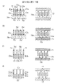
図7および図8は、本発明の第1の実施形態に係る櫛歯電極対形成方法の一連の工程を表す。この方法は、一対の櫛歯電極13,23や一対の櫛歯電極14,24を形成するための一手法であり、マイクロミラー素子X1の製造過程において利用することができる。図7および図8の左側には、図8(d)に示す一対の櫛歯電極E1,E2の形成過程を、一の断面の変化として表す。当該一の断面は、加工が施される材料基板(多層構造を有するウエハ)における部分断面である。また、図7および図8の右側には、加工が施される材料基板における、左側断面に対応する箇所およびその近傍の部分平面を表す(各左側断面図は、図7(a)の右側平面図の線VII−VIIに沿った断面図である)。櫛歯電極E1は、櫛歯電極13,14に相当し、導体部E1aと、導体部E1bと、これらの間の絶縁部E1cとからなる積層構造を有する。櫛歯電極E2は、櫛歯電極23,24に相当する。
7 and 8 show a series of steps of the comb electrode pair forming method according to the first embodiment of the present invention. This method is a method for forming the pair of comb-
櫛歯電極E1,E2の形成においては、まず、図7(a)に示すように、材料基板70上にプリ酸化膜パターン71’を形成する。材料基板70は、シリコン層70a,70bと、当該シリコン層70a,70b間の絶縁層70cとからなる積層構造を有するSOI基板である。シリコン層70a,70bは、不純物をドープすることにより導電性を付与されたシリコン材料よりなる。不純物としては、Bなどのp型不純物や、PおよびSbなどのn型不純物を採用することができる。絶縁層70cは例えば酸化シリコンよりなる。シリコン層70aの厚さは例えば10〜100μmであり、シリコン層70bの厚さは例えば50〜500μmであり、絶縁層70cの厚さは例えば0.3〜3μmである。プリ酸化膜パターン71’は、後出の酸化膜パターン71を形成するためのものであり、材料基板70のシリコン層70a上に形成される。プリ酸化膜パターン71’の形成においては、まず、CVD法により、シリコン層70aの表面に、厚さが例えば1μmとなるまで例えば酸化シリコンを成膜する。次に、シリコン層70a上の当該酸化膜について、所定のレジストパターンをマスクとしたドライエッチングまたはウエットエッチングによりパターニングする。ドライエッチングを採用する場合、エッチングガスとしては、例えば、CF4やCHF3などを採用することができる。ウエットエッチングを採用する場合、エッチング液としては、例えば、フッ酸とフッ化アンモニウムからなるバッファードフッ酸(BHF)を使用することができる。後出の酸化膜パターンについても、酸化物材料の成膜、酸化膜上のレジストパターンの形成、およびその後のエッチング処理、を経て形成される。
In forming the comb-tooth electrodes E1 and E2, first, as shown in FIG. 7A, a
次に、図7(b)に示すようにレジストパターン72を形成する。レジストパターン72は、プリ酸化膜パターン71’上のマスク部72a、および、シリコン層70a上のマスク部72bを含む。マスク部72aは、櫛歯電極E1に対応するパターン形状を有し、マスク部72bは、櫛歯電極E2に対応するパターン形状を有する。レジストパターン72の形成においては、まず、材料基板70のシリコン層70aの側に、プリ酸化膜パターン71’の上方から、液状のフォトレジストをスピンコーティングにより成膜する。次に、露光処理およびその後の現像処理を経て、当該フォトレジスト膜をパターニングする。フォトレジストとしては、例えば、AZP4210(AZエレクトロニックマテリアルズ製)やAZ1500(AZエレクトロニックマテリアルズ製)を使用することができる。後出のレジストパターンについても、このようなフォトレジストの成膜ならびにその後の露光処理および現象処理を経て、形成することができる。
Next, a resist
次に、図7(c)に示すように、レジストパターン72をマスクとしてプリ酸化膜パターン71’に対してエッチング処理を施すことにより、マスク部71aを含む酸化膜パターン71を形成する。マスク部71aは、プリ酸化膜パターン71’において、レジストパターン72のマスク部72aにマスクされた箇所であり、マスク部72aと実質的に同じパターン形状を有し、従って、櫛歯電極E1に対応するパターン形状を有する。
Next, as shown in FIG. 7C, the pre-oxide film pattern 71 'is etched using the resist
次に、図7(d)に示すように、酸化膜パターン71およびレジストパターン72をマスクとして、DRIE(deep reactive ion etching)により、シリコン層70aに対して絶縁層70cに至るまで異方性エッチング処理を行う。本エッチング処理により、櫛歯電極E1の導体部E1aおよび残存マスク部70a’が形成される。導体部E1aは、シリコン層70aにおいて、重なり合うマスク部71a,72aによりマスクされた箇所である。残存マスク部70a’は、シリコン層70aにおいてマスク部72bによりマスクされた箇所である。また、DRIEでは、エッチングと側壁保護とを交互に行うBoschプロセスにおいて、良好なエッチング処理を行うことができる。本工程および後出のDRIEについては、このようなBoschプロセスを採用してもよい。
Next, as shown in FIG. 7D, anisotropic etching is performed from the
次に、図8(a)に示すように、絶縁層70cにおいて前工程にて露出した箇所をエッチング除去する。具体的には、絶縁層70cに対してシリコン層70aの側からシリコン層70bに至るまでエッチング処理を施す。エッチング処理としては、エッチングガスとして例えばCF4やCHF3を使用して行うドライエッチングや、エッチング液として例えばBHFを使用して行うウエットエッチングを採用することができる。本エッチング処理により、櫛歯電極E1の絶縁部E1cおよび残存マスク部70c’が形成される。絶縁部E1cは、絶縁層70cにおいて、導体部E1aによりマスクされた箇所である。残存マスク部70c’は、絶縁層70cにおいて残存マスク部70a’によりマスクされた箇所である。
Next, as shown in FIG. 8A, the portions exposed in the previous step in the insulating
次に、図8(b)に示すように、例えば剥離液を作用させることにより、レジストパターン72を除去する。剥離液としては、例えばAZリムーバ700(AZエレクトロニックマテリアルズ製)を使用することができる。
Next, as shown in FIG. 8B, the resist
次に、図8(c)に示すように、DRIEにより、シリコン層70bに対してシリコン層70aの側から異方性エッチング処理を施し、残存マスク部70a’を除去しつつ、櫛歯電極E1の導体部E1bおよび櫛歯電極E2を成形する。導体部E1bは、シリコン層70bにおいて絶縁部E1cに接する箇所である。櫛歯電極E2は、シリコン層70bにおいて残存マスク部70c’にマスクされた箇所である。
Next, as shown in FIG. 8C, the
次に、図8(d)に示すように、酸化膜パターン71および残存マスク部70c’をエッチング除去する。エッチング手法としては、エッチングガスとして例えばCF4やCHF3を使用して行うドライエッチングや、エッチング液として例えばBHFを使用して行うウエットエッチングを採用することができる。以上の一連の工程を経ることにより、一対の櫛歯電極E1,E2(一対の櫛歯電極13,23や一対の櫛歯電極14,24)を形成することができる。
Next, as shown in FIG. 8D, the
本方法では、レジストパターン72のマスク部72a,72bは、材料基板70の同一面側においてパターン形成されるため、マスク部72a,72bの相対的な形成位置については高精度を達成することができる。これとともに、酸化膜パターン71のマスク部71aは、図7(c)を参照して上述した工程において、レジストパターン72をマスクとして使用して行うエッチング処理により、レジストパターン72のマスク部72aに対応したパターン形状に形成される。そのため、本方法では、マスク部71a,72bの相対的な形成位置については高精度を達成することができる。すなわち、本方法では、酸化膜パターン71のマスク部71aとレジストパターン72のマスク部72bとについて、材料基板70の同一面側において、セルフアライメント(具体的には、マスク部72bと同様にレジストパターン72に含まれるマスク部72aに対応した形状にマスク部71aがパターン形成されることにより、マスク部72bに対してマスク部71aが実質的に位置合わせされる事象)により、高精度に位置合わせすることができるのである。そして、図7(d)を参照して上述した工程では、マスク部71aの形状に対応した形状を有する導体部E1aが、マスク部72bの形状に対応した形状を有する残存マスク部70a’が、形成される。図8(a)を参照して上述した工程では、導体部E1a(従ってマスク部71a)の形状に対応した形状を有する絶縁部E1cが、残存マスク部70a’(従ってマスク部72b)の形状に対応した形状を有する残存マスク部70c’が、形成される。図8(c)を参照して上述した工程では、絶縁部E1c(従ってマスク部71a)の形状に対応した形状を有する導体部E1bが、残存マスク部70c’(従ってマスク部72b)の形状に対応した形状を有する櫛歯電極E2が、形成される。したがって、本方法によると、導体部E1a,E1bおよび絶縁部E1cからなる積層構造を有する櫛歯電極E1と、櫛歯電極E2とを、高いアライメント精度で形成することができるのである。
In this method, since the
加えて、本方法によると、櫛歯電極E1,E2を、素子厚さ方向における寸法について高い精度で形成することができる。素子厚さ方向における櫛歯電極E1の寸法は、材料基板70の厚さに相当する。素子厚さ方向における櫛歯電極E2の寸法は、材料基板70のシリコン層70bの厚さに相当する。材料基板70やそれに含まれるシリコン層70bの厚さについては高精度に設定し得るので、本方法によると、櫛歯電極E1,E2を、素子厚さ方向における寸法について高い精度で形成することができるのである。
In addition, according to this method, the comb-tooth electrodes E1 and E2 can be formed with high accuracy with respect to the dimension in the element thickness direction. The dimension of the comb-tooth electrode E <b> 1 in the element thickness direction corresponds to the thickness of the
図9および図10は、マイクロミラー素子X1の第1変形例であるマイクロミラー素子X2の断面図である。図9および図10は、各々、マイクロミラー素子X1にとっての図3および図4に相当する断面図である。マイクロミラー素子X2は、櫛歯電極13,14,23,24の電極歯13A,14A,23A,24Aが、揺動部10の非動作時に厚さ方向Hに対して所定方向に傾斜している点において、マイクロミラー素子X1と異なる。
9 and 10 are cross-sectional views of a micromirror element X2 that is a first modification of the micromirror element X1. 9 and 10 are cross-sectional views corresponding to FIGS. 3 and 4 for the micromirror element X1, respectively. In the micromirror element X2, the
図11および図12は、本発明の第2の実施形態に係る櫛歯電極対形成方法の一連の工程を表す。この方法は、マイクロミラー素子X2の一対の櫛歯電極13,23や一対の櫛歯電極14,24を形成するための一手法であり、マイクロミラー素子X2の製造過程において利用することができる。図11および図12においては、図12(d)に示す一対の櫛歯電極E3,E4の形成過程を、一の断面の変化として表す。当該一の断面は、加工が施される材料基板(多層構造を有するウエハ)における部分断面である。櫛歯電極E3は、マイクロミラー素子X2の櫛歯電極13,14に相当し、導体部E3aと、導体部E3bと、これらの間の絶縁部E3cとからなる積層構造を有する。櫛歯電極E4は、マイクロミラー素子X2の櫛歯電極23,24に相当する。
11 and 12 show a series of steps of the comb electrode pair forming method according to the second embodiment of the present invention. This method is a technique for forming the pair of
櫛歯電極E3,E4の形成においては、まず、図11(a)に示すように、材料基板70上にレジスト膜73を形成する。材料基板70については、第1の実施形態におけるのと同様であり、導電性を付与されたシリコン材料よりなるシリコン層70a,70b、および、例えば酸化シリコンよりなる絶縁層70cからなる積層構造を有する。レジスト膜73は、材料基板70のシリコン層70a,70bに対する後出の異方性エッチング処理の際にエッチングが最も速く進行する方向を材料基板70の厚さ方向に対して傾斜せしめるためのものであり、所定の厚さ変化を有する。当該傾斜の角度は例えば1〜5°である。レジスト膜73の形成においては、例えば、まず、材料基板70のシリコン層70bの側に液状のフォトレジストをスピンコーティングにより成膜する。フォトレジストとしては、例えば、AZP4210(AZエレクトロニックマテリアルズ製)やAZ1500(AZエレクトロニックマテリアルズ製)を使用することができる。次に、所定の光透過性変化を有するグレイマスクを使用して当該フォトレジスト膜を所定の程度に露光処理する。その後、現像処理を行うことにより、当該フォトレジスト膜を厚さ方向において部分的に除去する。このようにして、所望の厚さ変化を有するレジスト膜73を形成することができる。
In forming the comb-tooth electrodes E3 and E4, first, as shown in FIG. 11A, a resist
櫛歯電極E3,E4の形成においては、この後、形成目的が櫛歯電極E3,E4であること及びレジスト膜73の除去作業を含むこと以外は、図7(a)から図8(d)を参照して上述した第1の実施形態と同様にして、材料基板70に対して加工を施す。
In the formation of the comb-tooth electrodes E3 and E4, thereafter, except that the purpose of the formation is the comb-tooth electrodes E3 and E4 and the removal work of the resist
具体的には、まず、図11(b)に示すように、材料基板70のシリコン層70a上にプリ酸化膜パターン71’を形成する。次に、図11(c)に示すように、プリ酸化膜パターン71’上のマスク部72aとシリコン層70a上のマスク部72bとを含むレジストパターン72を形成する。本実施形態では、マスク部72aは、櫛歯電極E3に対応するパターン形状を有し、マスク部72bは、櫛歯電極E4に対応するパターン形状を有する。次に、図11(d)に示すように、レジストパターン72をマスクとしてプリ酸化膜パターン71’に対してエッチング処理を施すことにより、マスク部71aを含む酸化膜パターン71を形成する。マスク部71aは、プリ酸化膜パターン71’において、レジストパターン72のマスク部72aにマスクされた箇所であり、マスク部72aと実質的に同じパターン形状を有し、従って、本実施形態では、櫛歯電極E3に対応するパターン形状を有する。
Specifically, first, as shown in FIG. 11B, a
次に、図11(e)に示すように、酸化膜パターン71およびレジストパターン72をマスクとして、DRIEにより、シリコン層70aに対して絶縁層70cに至るまで異方性エッチング処理を行う。本エッチング処理時には、エッチング装置のチャンバ内の保持ステージに設置された材料基板70は、厚さ変化を有するレジスト膜73の存在に起因して、ステージ面に対して傾斜した姿勢にある。そのため、本エッチング処理におけるエッチング方向(エッチングが最も速く進行する方向)は、材料基板70の厚さ方向に対して傾斜することとなる。本エッチング処理により、櫛歯電極E3の導体部E3aおよび残存マスク部70a’が形成される。導体部E3aは、シリコン層70aにおいて、重なり合うマスク部71a,72aによりマスクされた箇所である。残存マスク部70a’は、シリコン層70aにおいてマスク部72bによりマスクされた箇所である。
Next, as shown in FIG. 11E, an anisotropic etching process is performed on the
次に、図12(a)に示すように、絶縁層70cに対してシリコン層70aの側からシリコン層70bに至るまでエッチング処理を施す。本エッチング処理により、櫛歯電極E3の絶縁部E3cおよび残存マスク部70c’が形成される。絶縁部E3cは、絶縁層70cにおいて、導体部E3aによりマスクされた箇所である。残存マスク部70c’は、絶縁層70cにおいて残存マスク部70a’によりマスクされた箇所である。次に、図12(b)に示すように、酸素アッシングなどにより、レジストパターン72を除去する。次に、図12(c)に示すように、DRIEにより、シリコン層70bに対してシリコン層70aの側から異方性エッチング処理を施し、残存マスク部70a’を除去しつつ、櫛歯電極E3の導体部E3bおよび櫛歯電極E4を成形する。本エッチング処理では、図11(e)を参照して上述したエッチング処理におけるのと同様に、エッチング方向は材料基板70の厚さ方向に対して傾斜している。導体部E3bは、シリコン層70bにおいて絶縁部E3cに接する箇所である。櫛歯電極E4は、シリコン層70bにおいて残存マスク部70c’にマスクされた箇所である。次に、図12(d)に示すように、酸化膜パターン71および残存マスク部70c’をエッチング除去する。また、レジスト膜73も除去する。以上の一連の工程を経ることにより、一対の櫛歯電極E3,E4(マイクロミラー素子X2の一対の櫛歯電極13,23や一対の櫛歯電極14,24)を形成することができる。
Next, as shown in FIG. 12A, the insulating
本方法では、第1の実施形態に関して上述したのと同様に、マスク部71a,72bの相対的な形成位置については高精度を達成することができる。すなわち、本方法では、酸化膜パターン71のマスク部71aとレジストパターン72のマスク部72bとについて、材料基板70の同一面側において、セルフアライメントにより、高精度に位置合わせすることができる。そして、図11(e)を参照して上述した工程では、マスク部71aの形状に対応した形状を有する導体部E3aが、マスク部72bの形状に対応した形状を有する残存マスク部70a’が、形成される。図12(a)を参照して上述した工程では、導体部E3a(従ってマスク部71a)の形状に対応した形状を有する絶縁部E3cが、残存マスク部70a’(従ってマスク部72b)の形状に対応した形状を有する残存マスク部70c’が、形成される。図12(c)を参照して上述した工程では、絶縁部E3c(従ってマスク部71a)の形状に対応した形状を有する導体部E3bが、残存マスク部70c’(従ってマスク部72b)の形状に対応した形状を有する櫛歯電極E4が、形成される。したがって、本方法によると、導体部E3a,E3bおよび絶縁部E3cからなる積層構造を有する櫛歯電極E3と、櫛歯電極E4とを、高いアライメント精度で形成することができるのである。
In this method, as described above with respect to the first embodiment, high accuracy can be achieved with respect to the relative formation positions of the
また、本方法によると、櫛歯電極E3,E4を、素子厚さ方向における寸法について高い精度で形成することができる。素子厚さ方向における櫛歯電極E3の寸法は、材料基板70の厚さに相当する。素子厚さ方向における櫛歯電極E4の寸法は、材料基板70のシリコン層70bの厚さに相当する。材料基板70やそれに含まれるシリコン層70bの厚さについては高精度に設定し得るので、本方法によると、櫛歯電極E3,E4を、素子厚さ方向における寸法について高い精度で形成することができるのである。
Moreover, according to this method, the comb-tooth electrodes E3 and E4 can be formed with high accuracy with respect to the dimension in the element thickness direction. The dimension of the comb electrode E <b> 3 in the element thickness direction corresponds to the thickness of the
加えて、本方法によると、所定の厚さ変化を有するレジスト膜73を利用することにより、材料基板70の厚さ方向ないし素子厚さ方向に対して所定の角度で傾斜した櫛歯電極E3,E4を形成することができる。
In addition, according to the present method, by using the resist
図13および図14は、マイクロミラー素子X1の第2変形例であるマイクロミラー素子X3の断面図である。図13および図14は、各々、マイクロミラー素子X1にとっての図3および図4に相当する断面図である。マイクロミラー素子X3は、櫛歯電極13,14ないし電極歯13A,14Aの導体部13a,14aが、揺動部10の非動作時に厚さ方向Hに対して所定方向に傾斜している点において、マイクロミラー素子X1と異なる。
13 and 14 are cross-sectional views of a micromirror element X3 that is a second modification of the micromirror element X1. 13 and 14 are cross-sectional views corresponding to FIGS. 3 and 4 for the micromirror element X1, respectively. The micromirror element X3 is such that the
図15および図16は、本発明の第3の実施形態に係る櫛歯電極対形成方法の一連の工程を表す。この方法は、マイクロミラー素子X3の一対の櫛歯電極13,23や一対の櫛歯電極14,24を形成するための一手法であり、マイクロミラー素子X3の製造過程において利用することができる。図15および図16においては、図16(d)に示す一対の櫛歯電極E5,E6の形成過程を、一の断面の変化として表す。当該一の断面は、加工が施される材料基板(多層構造を有するウエハ)における部分断面である。櫛歯電極E5は、マイクロミラー素子X3の櫛歯電極13,14に相当し、導体部E5aと、導体部E5bと、これらの間の絶縁部E5cとからなる積層構造を有する。櫛歯電極E6は、マイクロミラー素子X3の櫛歯電極23,24に相当する。
15 and 16 show a series of steps of the comb electrode pair forming method according to the third embodiment of the present invention. This method is a method for forming the pair of
櫛歯電極E5,E6の形成においては、まず、図15(a)に示すように、材料基板70上にレジスト膜73を形成する。材料基板70については、第1の実施形態におけるのと同様であり、導電性を付与されたシリコン材料よりなるシリコン層70a,70b、および、例えば酸化シリコンよりなる絶縁層70cからなる積層構造を有する。レジスト膜73については、第2の実施形態におけるのと同様であり、所定の厚さ変化を有する。
In forming the comb-tooth electrodes E5 and E6, first, a resist
櫛歯電極E5,E6の形成においては、この後、形成目的が櫛歯電極E5,E6であること及びレジスト膜73の除去作業を含むこと以外は、第1の実施形態において図7および図8を参照して上述したのと同様にして、材料基板70に対して加工を施す。
In the formation of the comb-tooth electrodes E5 and E6, after that, the object of formation is the comb-tooth electrodes E5 and E6 and the removal operation of the resist
具体的には、まず、図15(b)に示すように、材料基板70のシリコン層70a上にプリ酸化膜パターン71’を形成する。次に、図15(c)に示すように、プリ酸化膜パターン71’上のマスク部72aとシリコン層70a上のマスク部72bとを含むレジストパターン72を形成する。本実施形態では、マスク部72aは、櫛歯電極E5に対応するパターン形状を有し、マスク部72bは、櫛歯電極E6に対応するパターン形状を有する。次に、図15(d)に示すように、レジストパターン72をマスクとしてプリ酸化膜パターン71’に対してエッチング処理を施すことにより、マスク部71aを含む酸化膜パターン71を形成する。マスク部71aは、プリ酸化膜パターン71’において、レジストパターン72のマスク部72aにマスクされた箇所であり、マスク部72aと実質的に同じパターン形状を有し、従って、本実施形態では、櫛歯電極E5に対応するパターン形状を有する。次に、図15(e)に示すように、酸化膜パターン71およびレジストパターン72をマスクとして、DRIEにより、シリコン層70aに対して絶縁層70cに至るまで異方性エッチング処理を行う。本エッチング処理では、図11(e)を参照して上述したエッチング処理におけるのと同様に、エッチング方向は材料基板70の厚さ方向に対して傾斜している。本エッチング処理により、櫛歯電極E5の導体部E5aおよび残存マスク部70a’が形成される。導体部E5aは、シリコン層70aにおいて、重なり合うマスク部71a,72aによりマスクされた箇所である。残存マスク部70a’は、シリコン層70aにおいてマスク部72bによりマスクされた箇所である。
Specifically, first, as shown in FIG. 15B, a
次に、図16(a)に示すように、絶縁層70cに対してシリコン層70aの側からシリコン層70bに至るまでエッチング処理を施す。本エッチング処理により、櫛歯電極E5の絶縁部E5cおよび残存マスク部70c’が形成される。絶縁部E5cは、絶縁層70cにおいて、導体部E5aによりマスクされた箇所である。残存マスク部70c’は、絶縁層70cにおいて残存マスク部70a’によりマスクされた箇所である。次に、図16(b)に示すように、例えば剥離液を作用させることにより、レジストパターン72およびレジスト膜73を除去する。次に、図16(c)に示すように、DRIEにより、シリコン層70bに対してシリコン層70aの側から異方性エッチング処理を施し、残存マスク部70a’を除去しつつ、櫛歯電極E5の導体部E5bおよび櫛歯電極E6を成形する。導体部E5bは、シリコン層70bにおいて絶縁部E5cに接する箇所である。櫛歯電極E6は、シリコン層70bにおいて残存マスク部70c’にマスクされた箇所である。次に、図16(d)に示すように、酸化膜パターン71および残存マスク部70c’をエッチング除去する。以上の一連の工程を経ることにより、一対の櫛歯電極E5,E6(マイクロミラー素子X3の一対の櫛歯電極13,23や一対の櫛歯電極14,24)を形成することができる。
Next, as shown in FIG. 16A, the insulating
本方法では、第1の実施形態に関して上述したのと同様に、マスク部71a,72bの相対的な形成位置については高精度を達成することができる。すなわち、本方法では、酸化膜パターン71のマスク部71aとレジストパターン72のマスク部72bとについて、材料基板70の同一面側において、セルフアライメントにより、高精度に位置合わせすることができる。そして、図15(e)を参照して上述した工程では、マスク部71aの形状に対応した形状を有する導体部E5aが、マスク部72bの形状に対応した形状を有する残存マスク部70a’が、形成される。図16(a)を参照して上述した工程では、導体部E5a(従ってマスク部71a)の形状に対応した形状を有する絶縁部E5cが、残存マスク部70a’(従ってマスク部72b)の形状に対応した形状を有する残存マスク部70c’が、形成される。図16(c)を参照して上述した工程では、絶縁部E5c(従ってマスク部71a)の形状に対応した形状を有する導体部E5bが、残存マスク部70c’(従ってマスク部72b)の形状に対応した形状を有する櫛歯電極E6が、形成される。したがって、本方法によると、導体部E5a,E5bおよび絶縁部E5cからなる積層構造を有する櫛歯電極E5と、櫛歯電極E6とを、高いアライメント精度で形成することができるのである。
In this method, as described above with respect to the first embodiment, high accuracy can be achieved with respect to the relative formation positions of the
また、本方法によると、櫛歯電極E5,E6を、素子厚さ方向における寸法について高い精度で形成することができる。素子厚さ方向における櫛歯電極E5の寸法は、材料基板70の厚さに相当する。素子厚さ方向における櫛歯電極E6の寸法は、材料基板70のシリコン層70bの厚さに相当する。材料基板70やそれに含まれるシリコン層70bの厚さについては高精度に設定し得るので、本方法によると、櫛歯電極E5,E6を、素子厚さ方向における寸法について高い精度で形成することができるのである。
Moreover, according to this method, the comb-tooth electrodes E5 and E6 can be formed with high accuracy in the dimension in the element thickness direction. The dimension of the comb electrode E5 in the element thickness direction corresponds to the thickness of the material substrate. The dimension of the comb electrode E6 in the element thickness direction corresponds to the thickness of the
加えて、本方法によると、所定の厚さ変化を有するレジスト膜73を利用することにより、材料基板70の厚さ方向ないし素子厚さ方向に対して所定の角度で傾斜した櫛歯電極E5を形成することができる。
In addition, according to the present method, by using the resist
図17から図21は、本発明の第4の実施形態に係る櫛歯電極対形成方法を製造過程において利用して製造することのできるマイクロミラー素子X4を表す。図17は、マイクロミラー素子X4の平面図であり、図18は、マイクロミラー素子X4の一部省略平面図である。図19から図21は、各々、図17の線XIX−XIX、線XX−XX、および線XXI−XXIに沿った断面図である。 FIGS. 17 to 21 show a micromirror element X4 that can be manufactured by using the comb electrode pair forming method according to the fourth embodiment of the present invention in the manufacturing process. FIG. 17 is a plan view of the micromirror element X4, and FIG. 18 is a partially omitted plan view of the micromirror element X4. 19 to 21 are cross-sectional views taken along line XIX-XIX, line XX-XX, and line XXI-XXI in FIG. 17, respectively.
マイクロミラー素子X4は、揺動部30と、フレーム41と、一対のトーションバー42と、櫛歯電極43,44とを備え、MEMS技術の一種であるマイクロマシニング技術により、SOI基板である材料基板に対して加工を施すことによって製造されたものである。当該材料基板は、第1および第2シリコン層ならびに当該シリコン層間の絶縁層よりなる積層構造を有し、各シリコン層は、不純物のドープにより所定の導電性が付与されている。マイクロミラー素子X4における上述の各部位は主に第1シリコン層および/または第2シリコン層に由来して形成されるところ、図の明確化の観点より、図18においては、第1シリコン層に由来して絶縁層より紙面手前方向に突き出る部位について、斜線ハッチングを付して表す。また、図18は、マイクロミラー素子X4において第2シリコン層に由来する構造を表す。
The micromirror element X4 includes an
揺動部30は、ミラー支持部31と、アーム部32と、櫛歯電極33,34とを有する。
The oscillating
ミラー支持部31は、第1シリコン層に由来する部位であり、その表面には、光反射機能を有するミラー面31aが設けられている。ミラー面31aは、例えば、第1シリコン層上に成膜されたCr層およびその上のAu層よりなる積層構造を有する。また、アーム部32は、主に第1シリコン層に由来する部位であり、ミラー支持部31から延出する。
The
櫛歯電極33は、複数の電極歯33Aからなる。複数の電極歯33Aは、アーム部32から各々が延出し、且つ、アーム部32の延び方向に互いに離隔する。櫛歯電極34は、複数の電極歯34Aからなる。複数の電極歯34Aは、電極歯33Aとは反対の側にアーム部32から各々が延出し、且つ、アーム部32の延び方向に互いに離隔する。電極歯33A,34Aは、主に第1シリコン層に由来する部位である。本実施形態では、図17に示すように、電極歯33A,34Aの延び方向とアーム部32の延び方向とは直交し、電極歯33Aは、図19に示すように素子厚さ方向Hに平行に起立しており、電極歯34Aは、図20に示すように素子厚さ方向Hに平行に起立している。このような櫛歯電極33ないし電極歯33Aと櫛歯電極34ないし電極歯34Aとは、アーム部32を介して電気的に接続されている。
The
フレーム41は、図17に示すように揺動部30を囲む形状を有し、図19から図21に示すように、第1シリコン層に由来する導体部41aと、第2シリコン層に由来する導体部41bと、絶縁層に由来して導体部41a,41bの間に介在する絶縁部41cとからなる積層構造を有する。導体部41bについては図18にも示す。
The
一対のトーションバー42は、各々、主に第1シリコン層に由来する部位であり、揺動部30のアーム部32とフレーム41の導体部41aとに接続してこれらを連結する。トーションバー42により、アーム部32と導体部41aとは電気的に接続される。また、トーションバー42は、素子厚さ方向Hにおいて、図19および図20に示すようにアーム部32より薄肉であり、フレーム41の導体部41aよりも薄肉である。このような一対のトーションバー42は、揺動部30ないしミラー支持部31の揺動動作の揺動軸心A4を規定する。揺動軸心A4は、図1に示すように、アーム部32の延び方向と直交する。したがって、アーム部32の延び方向に直交する方向にアーム部32から延出する上述の電極歯33A,34Aの延び方向は、揺動軸心A4に対して平行である。このような揺動軸心A4は、好ましくは、揺動部30の重心またはその近傍を通る。
The pair of
櫛歯電極43は、櫛歯電極33と協働して静電引力を発生するための部位であり、複数の電極歯43Aからなる。複数の電極歯43Aは、フレーム41から各々が延出し、且つ、アーム部32の延び方向に互いに離隔する。また、櫛歯電極43は、主に第2シリコン層に由来する部位であり、図18に示すように、フレーム41の導体部41bに固定されている。図17に示すように、電極歯43Aの延び方向とアーム部32の延び方向とは直交し、電極歯43Aの延び方向は揺動軸心A4に対して平行である。また、図19に示すように、電極歯43Aは素子厚さ方向Hに平行に起立している。
The
このような櫛歯電極43は、櫛歯電極33と共に駆動機構を構成する。櫛歯電極33,43は、揺動部30の例えば非動作時には、図19および図21に示すように、互いに異なる高さに位置する。また、櫛歯電極33,43は、揺動部30の揺動動作時において互いに当接しないように、それらの電極歯33A,43Aが位置ずれした態様で配されている。
Such a comb-
櫛歯電極44は、櫛歯電極34と協働して静電引力を発生するための部位であり、複数の電極歯44Aからなる。複数の電極歯44Aは、フレーム41から各々が延出し、且つ、アーム部32の延び方向に互いに離隔する。また、櫛歯電極44は、主に第2シリコン層に由来する部位であり、図18に示すように、フレーム41の導体部41bに固定されている。櫛歯電極44ないし電極歯44Aは、フレーム41の導体部41bを介して櫛歯電極43ないし電極歯43Aと電気的に接続されている。図17に示すように、電極歯44Aの延び方向とアーム部32の延び方向とは直交し、電極歯44Aの延び方向は揺動軸心A4に対して平行である。また、図20に示すように、電極歯44Aは素子厚さ方向Hに平行に起立している。
The
このような櫛歯電極44は、櫛歯電極34と共に駆動機構を構成する。櫛歯電極34,44は、揺動部30の例えば非動作時には、図20および図21に示すように、互いに異なる高さに位置する。また、櫛歯電極34,44は、揺動部30の揺動動作時において互いに当接しないように、それらの電極歯34A,44Aが位置ずれした態様で配されている。
Such a comb-
マイクロミラー素子X4においては、櫛歯電極33,34,43,44に対して必要に応じて所定の電位を付与することにより、揺動部30ないしミラー支持部31を揺動軸心A4まわりに回転変位させることができる。櫛歯電極33,34に対する電位付与は、フレーム41の導体部41a、両トーションバー42、およびアーム部32を介して、実現することができる。櫛歯電極33,34は、例えばグラウンド接続される。一方、櫛歯電極43,44に対する電位付与は、フレーム41の導体部41bを介して、実現することができる。フレーム41の導体部41aと導体部41bとは、絶縁部41cにより電気的に分離されている。
In the micromirror element X4, by applying a predetermined potential to the
櫛歯電極33,34,43,44の各々に所定の電位を付与することにより櫛歯電極33,43間および櫛歯電極34,44間に所望の静電引力を発生させると、櫛歯電極33は櫛歯電極43に引き込まれ、且つ、櫛歯電極34は櫛歯電極44に引き込まれる。そのため、揺動部30ないしミラー支持部31は、揺動軸心A4まわりに揺動動作し、当該静電引力と各トーションバー42の捩り抵抗力の総和とが釣り合う角度まで回転変位する。釣り合い状態においては、櫛歯電極33,43は、例えば図22に示す配向をとり、櫛歯電極34,44も同様の配向をとる。このような揺動動作における回転変位量は、櫛歯電極33,34,43,44への付与電位を調整することにより、調節することができる。また、櫛歯電極33,43間の静電引力および櫛歯電極34,44間の静電引力を消滅させると、各トーションバー42はその自然状態に復帰し、揺動部30ないしミラー支持部31は、図19から図21に表れているような配向をとる。以上のような揺動部30ないしミラー支持部31の揺動駆動により、ミラー支持部31上に設けられたミラー面31aにて反射される光の反射方向を適宜切り換えることができる。
When a desired electrostatic attraction is generated between the comb-
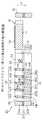
図23から図25は、本発明の第4の実施形態に係る櫛歯電極対形成方法の一連の工程を表す。この方法は、一対の櫛歯電極33,43や一対の櫛歯電極34,44を形成するための一手法であり、マイクロミラー素子X4の製造過程において利用することができる。図23および図24の左側には、図25(c)に示す一対の櫛歯電極E7,E8の形成過程を、一の断面の変化として表す。当該一の断面は、加工が施される材料基板(多層構造を有するウエハ)における部分断面である。また、図23から図25の右側には、加工が施される材料基板における、左側断面に対応する箇所およびその近傍の部分平面を表す(各左側断面図は、図23(a)の右側平面図の線XXIII−XXIIIに沿った断面図である)。櫛歯電極E7は櫛歯電極33,34に相当し、櫛歯電極E8は櫛歯電極43,44に相当する。
23 to 25 show a series of steps of the comb electrode pair forming method according to the fourth embodiment of the present invention. This method is a method for forming the pair of
櫛歯電極E7,E8の形成においては、まず、図23(a)に示すように、材料基板80上にプリ酸化膜パターン81’および酸化膜パターン82を形成する。材料基板80は、シリコン層80a,80bと、当該シリコン層80a,80b間の絶縁層80cとからなる積層構造を有するSOI基板である。シリコン層80a,80bは、不純物をドープすることにより導電性を付与されたシリコン材料よりなる。絶縁層80cは例えば酸化シリコンよりなる。シリコン層80aの厚さは例えば10〜100μmであり、シリコン層80bの厚さは、シリコン層80aの厚さより大きい限りにおいて例えば50〜500μmであり、絶縁層80cの厚さは例えば0.3〜3μmである。プリ酸化膜パターン81’は、後出の酸化膜パターン81を形成するためのものであり、材料基板80のシリコン層80a上に形成される。酸化膜パターン82は、櫛歯電極E8に対応するパターン形状を有するマスク部82aを含む。本工程では、プリ酸化膜パターン81’に対して公知の方法により位置合わせしつつ酸化膜パターン82をパターン形成する。
In forming the comb-tooth electrodes E7 and E8, first, as shown in FIG. 23A, a pre-oxide film pattern 81 'and an
次に、図23(b)に示すようにレジストパターン83を形成する。レジストパターン83は、プリ酸化膜パターン81’上のマスク部83a、および、シリコン層80a上のマスク部83bを含む。マスク部83aは、櫛歯電極E7に対応するパターン形状を有し、マスク部83bは、櫛歯電極E8に対応するパターン形状を有する。
Next, a resist
次に、図23(c)に示すように、レジストパターン83をマスクとしてプリ酸化膜パターン81’に対してエッチング処理を施すことにより、マスク部81aを含む酸化膜パターン81を形成する。マスク部81aは、プリ酸化膜パターン81’において、レジストパターン83のマスク部83aにマスクされた箇所であり、マスク部83aと実質的に同じパターン形状を有し、従って、櫛歯電極E7に対応するパターン形状を有する。
Next, as shown in FIG. 23C, the pre-oxide film pattern 81 'is etched using the resist
次に、図24(a)に示すように、酸化膜パターン81およびレジストパターン83をマスクとして、DRIEにより、シリコン層80aに対して絶縁層80cに至るまで異方性エッチング処理を行う。本エッチング処理により、櫛歯電極E7および残存マスク部80a’が形成される。櫛歯電極E7は、シリコン層80aにおいて、重なり合うマスク部81a,83aによりマスクされた箇所である。残存マスク部80a’は、シリコン層80aにおいてマスク部83bによりマスクされた箇所である。
Next, as shown in FIG. 24A, anisotropic etching is performed on the
次に、図24(b)に示すように、絶縁層80cにおいて前工程にて露出した箇所をエッチング除去する。具体的には、絶縁層80cに対してシリコン層80aの側からシリコン層80bに至るまでエッチング処理を施す。エッチング処理としては、エッチングガスとして例えばCF4やCHF3を使用して行うドライエッチングや、エッチング液として例えばBHFを使用して行うウエットエッチングを採用することができる。本エッチング処理により、残存マスク部80c’が形成される。残存マスク部80c’は、絶縁層80cにおいて残存マスク部80a’によりマスクされた箇所である。また、本エッチング処理を経ても、絶縁層80cにおいて櫛歯電極E7に接する箇所は残存する。
Next, as shown in FIG. 24B, the portions exposed in the previous step in the insulating
次に、図24(c)に示すように、剥離液を作用させることにより、レジストパターン83を除去する。剥離液としては、例えばAZリムーバ700(AZエレクトロニックマテリアルズ製)を使用することができる。
Next, as shown in FIG. 24C, the resist
次に、図25(a)に示すように、DRIEにより、シリコン層80bに対してシリコン層80aの側から異方性エッチング処理を施し、残存マスク部80a’を除去しつつ、櫛歯電極E8の一部E8aを形成する。当該一部E8aは、シリコン層80bにおいて残存マスク部80c’にマスクされた箇所である。また、本エッチング処理を経ても、シリコン層80bにおける櫛歯電極E7の図中下方の箇所は残存する。
Next, as shown in FIG. 25A, anisotropic etching is performed on the
次に、図25(b)に示すように、DRIEによりシリコン層80bに対して酸化膜パターン82の側から異方性エッチング処理を施すことによって、櫛歯電極E8の残りの一部E8bを形成し、且つ、シリコン層80bにおける櫛歯電極E7の図中下方の残存箇所を除去する。櫛歯電極E8の一部E8bは、シリコン層80bにおいて酸化膜パターン82のマスク部82aにマスクされた箇所である。
Next, as shown in FIG. 25B, the
次に、図25(c)に示すように、酸化膜パターン81,82、残存マスク部80c’、および絶縁層80cに由来して櫛歯電極E7の図中下方に残存している箇所を、エッチング除去する。エッチング手法としては、エッチングガスとして例えばCF4やCHF3を使用して行うドライエッチングや、エッチング液として例えばBHFを使用して行うウエットエッチングを採用することができる。以上の一連の工程を経ることにより、一対の櫛歯電極E7,E8(一対の櫛歯電極33,43,一対の櫛歯電極34,44)を形成することができる。
Next, as shown in FIG. 25C, the
本方法では、レジストパターン83のマスク部83a,83bは、材料基板80の同一面側においてパターン形成されるため、マスク部83a,83bの相対的な形成位置については高精度を達成することができる。これとともに、酸化膜パターン81のマスク部81aは、図23(c)を参照して上述した工程において、レジストパターン83をマスクとして使用して行うエッチング処理により、レジストパターン83のマスク部83aに対応したパターン形状に形成される。そのため、本方法では、マスク部81a,83bの相対的な形成位置については高精度を達成することができる。すなわち、本方法では、酸化膜パターン81のマスク部81aとレジストパターン83のマスク部83bとについて、材料基板80の同一面側において、セルフアライメント(具体的には、マスク部83bと同様にレジストパターン82に含まれるマスク部83aに対応した形状にマスク部81aがパターン形成されることにより、マスク部83bに対してマスク部81aが実質的に位置合わせされる事象)により、高精度に位置合わせすることができるのである。そして、図24(a)を参照して上述した工程では、マスク部81aの形状に対応した形状を有する櫛歯電極E7が、マスク部83bの形状に対応した形状を有する残存マスク部80a’が、形成される。図24(b)を参照して上述した工程では、残存マスク部80a’(従ってマスク部83b)の形状に対応した形状を有する残存マスク部80c’が形成される。図25(a)を参照して上述した工程では、残存マスク部80c’(従ってマスク部83b)の形状に対応した形状を有する櫛歯電極E8の一部E8a(櫛歯電極E8において櫛歯電極E7に近い側の部分)が形成される。したがって、本方法によると、櫛歯電極E7と、櫛歯電極E8の一部E8aとを、高いアライメント精度で形成することができる。本方法では、櫛歯電極E8の残りの一部E8b(櫛歯電極E8において櫛歯電極E7から遠い側の部分)は、図25(b)を参照して上述した工程にて、酸化膜パターン82のマスク部82aをマスクとして使用したエッチング処理により形成されるところ、一部E8bは、一部E8aほどには、櫛歯電極E7に対する形成位置について高精度に形成することが困難である。櫛歯電極E7に対する一部E8bの形成位置は、櫛歯電極E7に対する一部E8aの形成位置ほどには、高精度が求められない場合がある。そのような場合においては、本方法によっても、実質的に、相対的形成位置について高い精度で一対の櫛歯電極E7,E8を形成することができるのである。
In this method, since the
加えて、本方法によると、櫛歯電極E7,E8を、素子厚さ方向における寸法について高い精度で形成することができる。素子厚さ方向における櫛歯電極E7の寸法は、材料基板80のシリコン層80aの厚さに相当する。素子厚さ方向における櫛歯電極E8の寸法は、材料基板80のシリコン層80bの厚さに相当する。シリコン層80a,80bの厚さについては高精度に設定し得るので、本方法によると、櫛歯電極E7,E8を、素子厚さ方向における寸法について高い精度で形成することができるのである。
In addition, according to this method, the comb-tooth electrodes E7 and E8 can be formed with high accuracy with respect to the dimension in the element thickness direction. The dimension of the comb electrode E7 in the element thickness direction corresponds to the thickness of the
図26および図27は、マイクロミラー素子X4の変形例であるマイクロミラー素子X5の断面図である。図26および図27は、各々、マイクロミラー素子X4にとっての図19および図20に相当する断面図である。マイクロミラー素子X5は、櫛歯電極33,34の電極歯33A,34Aが、揺動部30の非動作時に厚さ方向Hに対して所定方向に傾斜している点において、マイクロミラー素子X4と異なる。
26 and 27 are cross-sectional views of a micromirror element X5 that is a modification of the micromirror element X4. 26 and 27 are cross-sectional views corresponding to FIGS. 19 and 20 for the micromirror element X4, respectively. The micromirror element X5 is different from the micromirror element X4 in that the
マイクロミラー素子X5では、揺動部30が回転変位して櫛歯電極33の電極歯33Aが部分的に櫛歯電極43の電極歯43Aに対面するとき、電極歯33Aは電極歯43Aに対して平行な配向、または平行に近い配向をとり得る。同様に、揺動部30が回転変位して櫛歯電極34の電極歯34Aが部分的に櫛歯電極44の電極歯44Aに対面するとき、電極歯34Aは電極歯44Aに対して平行な配向、または平行に近い配向をとり得る。したがってマイクロミラー素子X5においては、櫛歯電極33,43間および櫛歯電極34,44間にて安定した静電引力が生ずるように制御しやすい。
In the micromirror element X5, when the
図28から図30は、本発明の第5の実施形態に係る櫛歯電極対形成方法の一連の工程を表す。この方法は、マイクロミラー素子X5の一対の櫛歯電極33,43や一対の櫛歯電極34,44を形成するための一手法であり、マイクロミラー素子X5の製造過程において利用することができる。図28から図30においては、図30(c)に示す一対の櫛歯電極E9,E10の形成過程を、一の断面の変化として表す。当該一の断面は、加工が施される材料基板(多層構造を有するウエハ)における単一のマイクロミラー素子形成区画に含まれる櫛歯電極形成箇所の断面である。櫛歯電極E9は、マイクロミラー素子X5の櫛歯電極33,34に相当し、櫛歯電極E10は、マイクロミラー素子X5の櫛歯電極43,44に相当する。
28 to 30 show a series of steps of a comb electrode pair forming method according to the fifth embodiment of the present invention. This method is a technique for forming the pair of comb-
櫛歯電極E9,E10の形成においては、まず、図28(a)に示すように、第4の実施形態に関して図23(a)および図23(b)を参照して上述したのと同様にして、材料基板80上にプリ酸化膜パターン81’、酸化膜パターン82、およびレジストパターン83を形成する。本実施形態では、酸化膜パターン82は、櫛歯電極E10に対応するパターン形状を有するマスク部82aを含む。レジストパターン83は、プリ酸化膜パターン81’上のマスク部83a、および、シリコン層80a上のマスク部83bを含む。本実施形態では、マスク部83aは、櫛歯電極E9に対応するパターン形状を有し、マスク部83bは、櫛歯電極E10に対応するパターン形状を有する。
In forming the comb-tooth electrodes E9 and E10, first, as shown in FIG. 28 (a), the fourth embodiment is performed in the same manner as described above with reference to FIGS. 23 (a) and 23 (b). Then, a
次に、図28(b)に示すように、材料基板80上にレジスト膜84を形成する。レジスト膜84は、材料基板80のシリコン層80aに対する後出の異方性エッチング処理の際にエッチングが最も速く進行する方向を材料基板80の厚さ方向に対して傾斜せしめるためのものであり、所定の厚さ変化を有する。当該傾斜の角度は例えば1〜5°である。レジスト膜84の形成においては、例えば、まず、材料基板80のシリコン層80bの側に液状のフォトレジストをスピンコーティングにより成膜する。フォトレジストとしては、例えば、AZP4210(AZエレクトロニックマテリアルズ製)やAZ1500(AZエレクトロニックマテリアルズ製)を使用することができる。次に、所定の光透過性変化を有するグレイマスクを使用して当該フォトレジスト膜を所定の程度に露光処理する。その後、現像処理を行うことにより、当該フォトレジスト膜を厚さ方向において部分的に除去する。このようにして、所望の厚さ変化を有するレジスト膜84を形成することができる。
Next, as shown in FIG. 28B, a resist
櫛歯電極E9,E10の形成においては、この後、形成目的が櫛歯電極E9,E10であること及びレジスト膜84の除去作業を含むこと以外は、第4の実施形態において図23(c)から図25(c)を参照して上述したのと同様にして、材料基板80に対して加工を施す。
In the formation of the comb-tooth electrodes E9 and E10, the fourth embodiment is the same as that shown in FIG. 23C except that the purpose of the formation is the comb-tooth electrodes E9 and E10 and the removal operation of the resist
具体的には、まず、図28(c)に示すように、レジストパターン83をマスクとしてプリ酸化膜パターン81’に対してエッチング処理を施すことにより、マスク部81aを含む酸化膜パターン81を形成する。マスク部81aは、プリ酸化膜パターン81’において、レジストパターン83のマスク部83aにマスクされた箇所であり、マスク部83aと実質的に同じパターン形状を有し、従って、本実施形態では、櫛歯電極E9に対応するパターン形状を有する。
Specifically, as shown in FIG. 28C, first, an
次に、図29(a)に示すように、酸化膜パターン81およびレジストパターン83をマスクとして、DRIEにより、シリコン層80aに対して絶縁層80cに至るまで異方性エッチング処理を行う。本エッチング処理により、櫛歯電極E9および残存マスク部80a’が形成される。本エッチング処理時には、エッチング装置のチャンバ内の保持ステージに設置された材料基板80は、厚さ変化を有するレジスト膜84の存在に起因して、ステージ面に対して傾斜した姿勢にある。そのため、本エッチング処理におけるエッチング方向(エッチングが最も速く進行する方向)は、材料基板80の厚さ方向に対して傾斜することとなる。櫛歯電極E9は、シリコン層80aにおいて、重なり合うマスク部81a,83aによりマスクされた箇所である。残存マスク部80a’は、シリコン層80aにおいてマスク部83bによりマスクされた箇所である。次に、図29(b)に示すように、絶縁層80cに対してシリコン層80aの側からシリコン層80bに至るまでエッチング処理を施す。本エッチング処理により、残存マスク部80c’が形成される。残存マスク部80c’は、絶縁層80cにおいて残存マスク部80a’によりマスクされた箇所である。また、本エッチング処理を経ても、絶縁層80cにおいて櫛歯電極E9に接する箇所は残存する。次に、図29(c)に示すように、例えば剥離液を作用させることにより、レジストパターン83およびレジスト膜84を除去する。
Next, as shown in FIG. 29A, an anisotropic etching process is performed on the
次に、図30(a)に示すように、DRIEにより、シリコン層80bに対してシリコン層80aの側から異方性エッチング処理を施し、残存マスク部80a’を除去しつつ、櫛歯電極E10の一部E10aを形成する。当該一部E10aは、シリコン層80bにおいて残存マスク部80c’にマスクされた箇所である。また、本エッチング処理を経ても、シリコン層80bにおける櫛歯電極E9の図中下方の箇所は残存する。次に、図30(b)に示すように、DRIEによりシリコン層80bに対して酸化膜パターン82の側から異方性エッチング処理を施すことによって、櫛歯電極E10の残りの一部E10bを形成し、且つ、シリコン層80bにおける櫛歯電極E9の図中下方の残存箇所を除去する。櫛歯電極E10の一部E10bは、シリコン層80bにおいて酸化膜パターン82のマスク部82aにマスクされた箇所である。次に、図30(c)に示すように、酸化膜パターン81,82、残存マスク部80c’、および絶縁層80cに由来して櫛歯電極E9の図中下方に残存している箇所を、エッチング除去する。以上の一連の工程を経ることにより、一対の櫛歯電極E9,E10(マイクロミラー素子X5の一対の櫛歯電極33,43や一対の櫛歯電極34,44)を形成することができる。
Next, as shown in FIG. 30A, an anisotropic etching process is performed on the
本方法では、第4の実施形態に関して上述したのと同様に、マスク部81a,83bの相対的な形成位置については高精度を達成することができる。すなわち、本方法では、酸化膜パターン81のマスク部81aとレジストパターン83のマスク部83bとについて、材料基板80の同一面側において、セルフアライメントにより、高精度に位置合わせすることができる。そして、図29(a)を参照して上述した工程では、マスク部81aの形状に対応した形状を有する櫛歯電極E9が、マスク部83bの形状に対応した形状を有する残存マスク部80a’が、形成される。図29(b)を参照して上述した工程では、残存マスク部80a’(従ってマスク部83b)の形状に対応した形状を有する残存マスク部80c’が形成される。図30(a)を参照して上述した工程では、残存マスク部80c’(従ってマスク部83b)の形状に対応した形状を有する櫛歯電極E10の一部E10a(櫛歯電極E10において櫛歯電極E9に近い側の部分)が形成される。したがって、本方法によると、櫛歯電極E9と、櫛歯電極E10の一部E10aとを、相対的形成位置について高い精度で形成することができる。本方法では、櫛歯電極E10の残りの一部E10b(櫛歯電極E10において櫛歯電極E9から遠い側の部分)は、図30(b)を参照して上述した工程にて、酸化膜パターン82のマスク部82aをマスクとして使用したエッチング処理により形成されるところ、一部E10bは、一部E10aほどには、櫛歯電極E9に対する形成位置について高精度に形成することが困難である。櫛歯電極E9に対する一部E10bの形成位置は、櫛歯電極E9に対する一部E10aの形成位置ほどには、高精度が求められない場合がある。そのような場合においては、本方法によっても、実質的に、相対的形成位置について高い精度で一対の櫛歯電極E9,E10を形成することができるのである。
In this method, as described above with respect to the fourth embodiment, high accuracy can be achieved with respect to the relative formation positions of the
また、本方法によると、櫛歯電極E9,E10を、素子厚さ方向における寸法について高い精度で形成することができる。素子厚さ方向における櫛歯電極E9の寸法は、材料基板80のシリコン層80aの厚さに相当する。素子厚さ方向における櫛歯電極E10の寸法は、材料基板80のシリコン層80bの厚さに相当する。シリコン層80a,80bの厚さについては高精度に設定し得るので、本方法によると、櫛歯電極E9,E10を、素子厚さ方向における寸法について高い精度で形成することができるのである。
Moreover, according to this method, the comb-tooth electrodes E9 and E10 can be formed with high accuracy with respect to the dimension in the element thickness direction. The dimension of the comb electrode E9 in the element thickness direction corresponds to the thickness of the
加えて、本方法によると、所定の厚さ変化を有するレジスト膜84を利用することにより、材料基板80の厚さ方向ないし素子厚さ方向に対して所定の角度で傾斜した櫛歯電極E9を形成することができる。
In addition, according to the present method, by using the resist
本発明の櫛歯電極対形成方法は、回転変位可能な揺動部を備えるマイクロ揺動素子において揺動部を駆動するための櫛歯電極対を形成する際に限らず、マイクロ揺動素子において揺動部の回転変位量を検出するための櫛歯電極対を形成する際にも、利用可能である。当該検出用櫛歯電極対とは、例えば、当該櫛歯電極対の配向変化に起因する当該櫛歯電極対型コンデンサの静電容量変化に基づいて揺動部の回転変位量を検出するためのものである。 The comb-tooth electrode pair forming method of the present invention is not limited to forming a comb-tooth electrode pair for driving the rocking part in a micro-oscillating element having a rocking part that can be rotationally displaced. The present invention can also be used when forming a comb electrode pair for detecting the rotational displacement amount of the swinging portion. The comb electrode pair for detection is, for example, for detecting the rotational displacement amount of the oscillating portion based on the capacitance change of the comb electrode pair capacitor caused by the change in the orientation of the comb electrode pair. Is.
X1,X2,X3,X4,X5,X6 マイクロミラー素子
10,30 揺動部
11,31,61 ミラー支持部
12,32 アーム部
13,14,23,24,33,34,43,44 櫛歯電極
13A,14A,23A,24A,33A,34A,43A,44A 電極歯
21,41,62 フレーム
22,42,63 トーションバー
70,80 材料基板
70a,70b,80a,80b シリコン層
70c,80c 絶縁層
71’,81’ プリ酸化膜パターン
71,81,82 酸化膜パターン
72,83 レジストパターン
73,84 レジスト膜
X1, X2, X3, X4, X5, X6
Claims (2)
前記一対の櫛歯電極は、前記第1導体層に由来する第1導体部と、前記第2導体層に由来する第2導体部と、前記絶縁層に由来する絶縁部とからなる積層構造を有する第1櫛歯電極、および、前記第2導体層に由来する第2櫛歯電極からなり、
前記第1導体層上にプリ第1マスクパターンを形成する工程と、
前記プリ第1マスクパターン上の第1櫛歯電極用の第1マスク部、および、前記第1導体層上の第2櫛歯電極用の第2マスク部、を含む第2マスクパターンを、前記プリ第1マスクパターン上および前記第1導体層上にわたって形成する工程と、
前記第2マスクパターンを介して前記プリ第1マスクパターンに対してエッチング処理を施し、前記第2マスクパターンの前記第1マスク部に対応するパターン形状を有する第1櫛歯電極用の第3マスク部、を含む第1マスクパターンを、前記プリ第1マスクパターンから形成する、第1エッチング工程と、
前記第1および第2マスクパターンを介して前記第1導体層に対して前記絶縁層に至るまでエッチング処理を施し、重なり合う前記第1および第3マスク部にマスクされた第1導体部、および、前記第2マスク部にマスクされた第1残存マスク部を、前記第1導体層において前記材料基板の厚さ方向に対して傾斜をもって形成する、第2エッチング工程と、
前記絶縁層に対して第1導体層側から前記第2導体層に至るまでエッチング処理を施し、前記第1導体部にマスクされた絶縁部、および、前記第1残存マスク部にマスクされた第2残存マスク部を、前記絶縁層において形成する、第3エッチング工程と、
前記第2マスクパターンを除去する工程と、
前記第2導体層に対して第1導体層側からエッチング処理を施し、前記第1残存マスク部を除去しつつ、前記絶縁部に接する第2導体部、および、前記第2残存マスク部にマスクされた第2櫛歯電極を、前記第2導体層において形成する、第4エッチング工程と、を含み、
前記第2エッチング工程における前記傾斜は、前記第1櫛歯電極の電極歯と前記第2櫛歯電極の電極歯とが部分的に対面するとき、それらが互いに平行な配向となるような傾斜である、櫛歯電極対形成方法。 By processing the material substrate having a laminated structure composed of the first conductor layer, the second conductor layer, and the insulating layer between the first and second conductor layers, the material substrate is relatively displaced, It is a method for forming a pair of comb electrodes that can take a posture in which the electrode teeth that each has can partially face each other,
The pair of comb electrodes have a laminated structure including a first conductor portion derived from the first conductor layer, a second conductor portion derived from the second conductor layer, and an insulating portion derived from the insulating layer. A first comb electrode having a second comb electrode derived from the second conductor layer,
Forming a pre-first mask pattern on the first conductor layer;
A second mask pattern including a first mask portion for a first comb electrode on the pre-first mask pattern and a second mask portion for a second comb electrode on the first conductor layer; Forming over the pre-first mask pattern and the first conductor layer;
A third mask for a first comb electrode having a pattern shape corresponding to the first mask portion of the second mask pattern, wherein the pre-first mask pattern is etched through the second mask pattern. Forming a first mask pattern including a portion from the pre-first mask pattern; and
Etching the first conductor layer through the first and second mask patterns to reach the insulating layer, and the first conductor part masked by the overlapping first and third mask parts; and the first remaining mask portion that is masked in the second mask part is formed with inclined to the thickness direction of the material substrate in said first conductor layer, a second etching step,
Etching is performed on the insulating layer from the first conductor layer side to the second conductor layer, and the insulating portion masked by the first conductor portion and the first mask portion masked by the first remaining mask portion (2) a third etching step for forming a remaining mask portion in the insulating layer;
Removing the second mask pattern;
Etching the second conductor layer from the first conductor layer side, removing the first remaining mask portion, and masking the second conductor portion in contact with the insulating portion and the second remaining mask portion the second comb-tooth electrodes, formed in said second conductor layer, and a fourth etching step, only including,
The inclination in the second etching step is such that when the electrode teeth of the first comb electrode and the electrode teeth of the second comb electrode partially face each other, they are oriented parallel to each other. A method for forming a comb electrode pair.
前記一対の櫛歯電極は、前記第1導体層に由来する第1櫛歯電極、および、前記第2導体層に由来する第2櫛歯電極からなり、
前記第1導体層上にプリ第1マスクパターンを形成する工程と、
前記プリ第1マスクパターン上の第1櫛歯電極用の第1マスク部、および、前記第1導体層上の第2櫛歯電極用の第2マスク部、を含む第2マスクパターンを、前記プリ第1マスクパターン上および前記第1導体層上にわたって形成する工程と、
前記第2マスクパターンを介して前記プリ第1マスクパターンに対してエッチング処理を施し、前記第2マスクパターンの前記第1マスク部に対応するパターン形状を有する第1櫛歯電極用の第3マスク部、を含む第1マスクパターンを、前記プリ第1マスクパターンから形成する、第1エッチング工程と、
第2櫛歯電極用の第4マスク部を含む第3マスクパターンを前記第2導体層上に形成す
る工程と、
前記第1および第2マスクパターンを介して前記第1導体層に対して前記絶縁層に至るまでエッチング処理を施し、重なり合う前記第1および第3マスク部にマスクされた第1櫛歯電極、および、前記第2マスク部にマスクされた第1残存マスク部を、前記第1導体層において前記材料基板の厚さ方向に対して傾斜をもって形成する、第2エッチング工程と、
前記絶縁層に対して第1導体層側から前記第2導体層に至るまでエッチング処理を施し、前記第1残存マスク部にマスクされた第2残存マスク部を、前記絶縁層において形成する、第3エッチング工程と、
前記第2マスクパターンを除去する工程と、
前記第2導体層に対して第1導体層側から当該第2導体層の厚さ方向の途中までエッチング処理を施し、前記第1残存マスク部を除去しつつ、前記第2残存マスク部にマスクされた第2櫛歯電極の一部を、前記第2導体層において形成する、第4エッチング工程と、
前記第3マスクパターンを介して前記第2導体層に対してエッチング処理を施し、前記第2櫛歯電極の残部を形成する、第5エッチング工程と、を含み、
前記第2エッチング工程における前記傾斜は、前記第1櫛歯電極の電極歯と前記第2櫛歯電極の電極歯とが部分的に対面するとき、それらが互いに平行な配向となるような傾斜である、櫛歯電極対形成方法。 By processing the material substrate having a laminated structure composed of the first conductor layer, the second conductor layer, and the insulating layer between the first and second conductor layers, the material substrate is relatively displaced, It is a method for forming a pair of comb electrodes that can take a posture in which the electrode teeth that each has can partially face each other,
The pair of comb electrodes are composed of a first comb electrode derived from the first conductor layer and a second comb electrode derived from the second conductor layer,
Forming a pre-first mask pattern on the first conductor layer;
A second mask pattern including a first mask portion for a first comb electrode on the pre-first mask pattern and a second mask portion for a second comb electrode on the first conductor layer; Forming over the pre-first mask pattern and the first conductor layer;
A third mask for a first comb electrode having a pattern shape corresponding to the first mask portion of the second mask pattern, wherein the pre-first mask pattern is etched through the second mask pattern. Forming a first mask pattern including a portion from the pre-first mask pattern; and
A third mask pattern including a fourth mask portion for the second comb electrode is formed on the second conductor layer.
And the process
Etching the first conductor layer through the first and second mask patterns up to the insulating layer, and masking the first and third mask portions overlapping each other; and Forming a first residual mask portion masked by the second mask portion with an inclination with respect to a thickness direction of the material substrate in the first conductor layer; and
Etching the insulating layer from the first conductor layer side to the second conductor layer to form a second remaining mask portion masked by the first remaining mask portion in the insulating layer; 3 etching steps;
Removing the second mask pattern;
Etching is performed on the second conductor layer from the first conductor layer side to the middle in the thickness direction of the second conductor layer, and the second remaining mask portion is masked while removing the first remaining mask portion. Forming a part of the second comb-teeth electrode formed in the second conductor layer;
Etching the second conductor layer through the third mask pattern to form the remaining portion of the second comb electrode, and a fifth etching step.
The inclination in the second etching step is such that when the electrode teeth of the first comb electrode and the electrode teeth of the second comb electrode partially face each other, they are oriented parallel to each other. A method for forming a comb electrode pair.
Priority Applications (5)
| Application Number | Priority Date | Filing Date | Title |
|---|---|---|---|
| JP2005069155A JP4573676B2 (en) | 2005-03-11 | 2005-03-11 | Comb electrode pair forming method |
| TW095104910A TWI309069B (en) | 2005-03-11 | 2006-02-14 | Method of making comb-teeth electrode pair |
| KR1020060018003A KR100786739B1 (en) | 2005-03-11 | 2006-02-24 | Method of forming comb-shaped electrode pairs |
| CNB2006100597450A CN100410724C (en) | 2005-03-11 | 2006-03-06 | Manufacturing method of making comb-teeth electrode pair |
| US11/371,089 US7439184B2 (en) | 2005-03-11 | 2006-03-09 | Method of making comb-teeth electrode pair |
Applications Claiming Priority (1)
| Application Number | Priority Date | Filing Date | Title |
|---|---|---|---|
| JP2005069155A JP4573676B2 (en) | 2005-03-11 | 2005-03-11 | Comb electrode pair forming method |
Publications (2)
| Publication Number | Publication Date |
|---|---|
| JP2006247793A JP2006247793A (en) | 2006-09-21 |
| JP4573676B2 true JP4573676B2 (en) | 2010-11-04 |
Family
ID=36970541
Family Applications (1)
| Application Number | Title | Priority Date | Filing Date |
|---|---|---|---|
| JP2005069155A Active JP4573676B2 (en) | 2005-03-11 | 2005-03-11 | Comb electrode pair forming method |
Country Status (5)
| Country | Link |
|---|---|
| US (1) | US7439184B2 (en) |
| JP (1) | JP4573676B2 (en) |
| KR (1) | KR100786739B1 (en) |
| CN (1) | CN100410724C (en) |
| TW (1) | TWI309069B (en) |
Families Citing this family (16)
| Publication number | Priority date | Publication date | Assignee | Title |
|---|---|---|---|---|
| JP4138736B2 (en) * | 2004-12-02 | 2008-08-27 | 富士通株式会社 | Micro oscillating device |
| JP4534931B2 (en) * | 2005-09-27 | 2010-09-01 | パナソニック電工株式会社 | Method for manufacturing vertical comb actuator |
| JP4321507B2 (en) * | 2005-09-27 | 2009-08-26 | パナソニック電工株式会社 | Method for manufacturing vertical comb actuator |
| KR100790879B1 (en) | 2006-06-13 | 2008-01-03 | 삼성전자주식회사 | Manufacturing method for the comb electrodes of the MEMS device |
| KR100790878B1 (en) | 2006-06-13 | 2008-01-03 | 삼성전자주식회사 | Etching Method for decoupled comb electrodes by self-alignment |
| WO2008072248A2 (en) | 2006-12-14 | 2008-06-19 | Ramot At Tel-Aviv University Ltd. | Tilting actuator with close-gap electrodes |
| JP4477659B2 (en) * | 2007-06-29 | 2010-06-09 | 富士通株式会社 | Micro oscillating device and micro oscillating device array |
| JP2009014768A (en) | 2007-06-29 | 2009-01-22 | Fujitsu Ltd | Micro electro mechanical systems device and method of manufacturing the same |
| JP2009113128A (en) * | 2007-11-02 | 2009-05-28 | Fujitsu Ltd | Micro-oscillating element and its manufacturing method |
| DE102008005521B4 (en) | 2008-01-23 | 2019-01-03 | Robert Bosch Gmbh | Capacitive transducer and method of making the same |
| JP5056633B2 (en) * | 2008-07-14 | 2012-10-24 | 富士通株式会社 | Micro oscillating device, micro oscillating device array, and optical switching device |
| JP2011095621A (en) * | 2009-10-30 | 2011-05-12 | Furukawa Electric Co Ltd:The | Method of manufacturing optical switch element, optical switch element, optical switch device and method of manufacturing mems element |
| CN103086316B (en) * | 2011-10-28 | 2015-07-22 | 中国科学院上海微系统与信息技术研究所 | MEMS vertical comb micro-mirror surface driver manufacturing method |
| JP6927530B2 (en) * | 2018-11-16 | 2021-09-01 | 国立大学法人 東京大学 | Manufacturing method of comb-tooth type element |
| CN113994175A (en) * | 2019-06-07 | 2022-01-28 | 株式会社村田制作所 | Measuring instrument |
| CN111446359B (en) * | 2020-05-15 | 2023-05-30 | 京东方科技集团股份有限公司 | Piezoelectric device, manufacturing method thereof, electronic device and control method |
Citations (3)
| Publication number | Priority date | Publication date | Assignee | Title |
|---|---|---|---|---|
| JP2003057574A (en) * | 2001-08-20 | 2003-02-26 | Fujitsu Ltd | Manufacturing method for micromirror element and the micromirror element manufactured by the same |
| JP2003529312A (en) * | 2000-03-24 | 2003-09-30 | オニックス マイクロシステムズ インコーポレイテッド | Multilayer self-aligned vertical comb drive electrostatic actuator and method of manufacturing the same |
| JP2004219839A (en) * | 2003-01-16 | 2004-08-05 | Sony Corp | Three-dimensional structure and its manufacturing method, and electronic equipment |
Family Cites Families (13)
| Publication number | Priority date | Publication date | Assignee | Title |
|---|---|---|---|---|
| JP3178123B2 (en) * | 1992-02-25 | 2001-06-18 | 富士電機株式会社 | Method of manufacturing comb-type actuator |
| JPH10190007A (en) | 1996-12-25 | 1998-07-21 | Mitsubishi Materials Corp | Manufacture of semiconductor inertia sensor |
| JPH10270714A (en) | 1997-03-26 | 1998-10-09 | Mitsubishi Materials Corp | Manufacture of semiconductor inertia sensor |
| JPH11214706A (en) * | 1998-01-27 | 1999-08-06 | Toyota Motor Corp | Semiconductor sensor and its manufacture |
| US6287885B1 (en) * | 1998-05-08 | 2001-09-11 | Denso Corporation | Method for manufacturing semiconductor dynamic quantity sensor |
| JP4265016B2 (en) | 1998-05-08 | 2009-05-20 | 株式会社デンソー | Manufacturing method of semiconductor dynamic quantity sensor |
| US6229640B1 (en) * | 1999-08-11 | 2001-05-08 | Adc Telecommunications, Inc. | Microelectromechanical optical switch and method of manufacture thereof |
| JP2003015064A (en) * | 2001-07-04 | 2003-01-15 | Fujitsu Ltd | Micro mirror element |
| US6713367B2 (en) | 2001-08-28 | 2004-03-30 | The Board Of Trustees Of The Leland Stanford Junior University | Self-aligned vertical combdrive actuator and method of fabrication |
| JP2003241120A (en) | 2002-02-22 | 2003-08-27 | Japan Aviation Electronics Industry Ltd | Optical device |
| JP3987382B2 (en) * | 2002-06-11 | 2007-10-10 | 富士通株式会社 | Micromirror device and manufacturing method thereof |
| JP2005088188A (en) * | 2003-08-12 | 2005-04-07 | Fujitsu Ltd | Micro-oscillation element and method for driving the same |
| JP4252889B2 (en) | 2003-08-12 | 2009-04-08 | 富士通株式会社 | Manufacturing method of microstructure |
-
2005
- 2005-03-11 JP JP2005069155A patent/JP4573676B2/en active Active
-
2006
- 2006-02-14 TW TW095104910A patent/TWI309069B/en not_active IP Right Cessation
- 2006-02-24 KR KR1020060018003A patent/KR100786739B1/en active IP Right Grant
- 2006-03-06 CN CNB2006100597450A patent/CN100410724C/en not_active Expired - Fee Related
- 2006-03-09 US US11/371,089 patent/US7439184B2/en active Active
Patent Citations (4)
| Publication number | Priority date | Publication date | Assignee | Title |
|---|---|---|---|---|
| JP2003529312A (en) * | 2000-03-24 | 2003-09-30 | オニックス マイクロシステムズ インコーポレイテッド | Multilayer self-aligned vertical comb drive electrostatic actuator and method of manufacturing the same |
| JP2004500252A (en) * | 2000-03-24 | 2004-01-08 | オニックス マイクロシステムズ インコーポレイテッド | Multilayer self-aligned vertical comb drive electrostatic actuator and method of manufacturing the same |
| JP2003057574A (en) * | 2001-08-20 | 2003-02-26 | Fujitsu Ltd | Manufacturing method for micromirror element and the micromirror element manufactured by the same |
| JP2004219839A (en) * | 2003-01-16 | 2004-08-05 | Sony Corp | Three-dimensional structure and its manufacturing method, and electronic equipment |
Also Published As
| Publication number | Publication date |
|---|---|
| US7439184B2 (en) | 2008-10-21 |
| US20060203319A1 (en) | 2006-09-14 |
| TWI309069B (en) | 2009-04-21 |
| KR20060097593A (en) | 2006-09-14 |
| JP2006247793A (en) | 2006-09-21 |
| KR100786739B1 (en) | 2007-12-18 |
| CN1831579A (en) | 2006-09-13 |
| TW200638505A (en) | 2006-11-01 |
| CN100410724C (en) | 2008-08-13 |
Similar Documents
| Publication | Publication Date | Title |
|---|---|---|
| JP4573676B2 (en) | Comb electrode pair forming method | |
| US7453182B2 (en) | Micro oscillating element | |
| US7476950B2 (en) | Micro-oscillating element and method of making the same | |
| JP5470767B2 (en) | Micro movable element manufacturing method | |
| JP4919750B2 (en) | Microstructure manufacturing method and microstructure | |
| JP4477659B2 (en) | Micro oscillating device and micro oscillating device array | |
| US7903313B2 (en) | Micro movable element | |
| JP4138736B2 (en) | Micro oscillating device | |
| JP4464186B2 (en) | Micro oscillating device | |
| JP5240203B2 (en) | Micro movable element and micro movable element array | |
| JP4285005B2 (en) | Three-dimensional structure, manufacturing method thereof, and electronic device | |
| JP4598795B2 (en) | Micro oscillating device and micro oscillating device array | |
| JP4150003B2 (en) | Manufacturing method of microstructure and microstructure | |
| JP2009113128A (en) | Micro-oscillating element and its manufacturing method | |
| JP5309905B2 (en) | Micro movable element, micro movable element array, and optical switching device | |
| JP4129045B2 (en) | Micro oscillating element and movable functional element | |
| JP4537439B2 (en) | Micro oscillating device | |
| JP2005046958A (en) | Micro structure | |
| JP4445027B2 (en) | Micromirror element and micromirror array | |
| KR100825626B1 (en) | Microstructure | |
| JP2010038941A (en) | Micro structure and micro element composed of micro structure |
Legal Events
| Date | Code | Title | Description |
|---|---|---|---|
| A131 | Notification of reasons for refusal |
Free format text: JAPANESE INTERMEDIATE CODE: A131 Effective date: 20090317 |
|
| A977 | Report on retrieval |
Free format text: JAPANESE INTERMEDIATE CODE: A971007 Effective date: 20090319 |
|
| A521 | Request for written amendment filed |
Free format text: JAPANESE INTERMEDIATE CODE: A523 Effective date: 20090514 |
|
| A131 | Notification of reasons for refusal |
Free format text: JAPANESE INTERMEDIATE CODE: A131 Effective date: 20100126 |
|
| A521 | Request for written amendment filed |
Free format text: JAPANESE INTERMEDIATE CODE: A523 Effective date: 20100329 |
|
| TRDD | Decision of grant or rejection written | ||
| A01 | Written decision to grant a patent or to grant a registration (utility model) |
Free format text: JAPANESE INTERMEDIATE CODE: A01 Effective date: 20100810 |
|
| A01 | Written decision to grant a patent or to grant a registration (utility model) |
Free format text: JAPANESE INTERMEDIATE CODE: A01 |
|
| A61 | First payment of annual fees (during grant procedure) |
Free format text: JAPANESE INTERMEDIATE CODE: A61 Effective date: 20100817 |
|
| R150 | Certificate of patent or registration of utility model |
Ref document number: 4573676 Country of ref document: JP Free format text: JAPANESE INTERMEDIATE CODE: R150 Free format text: JAPANESE INTERMEDIATE CODE: R150 |
|
| FPAY | Renewal fee payment (event date is renewal date of database) |
Free format text: PAYMENT UNTIL: 20130827 Year of fee payment: 3 |