JP4554635B2 - Pattern inspection apparatus, pattern inspection method, and program - Google Patents
Pattern inspection apparatus, pattern inspection method, and program Download PDFInfo
- Publication number
- JP4554635B2 JP4554635B2 JP2007075962A JP2007075962A JP4554635B2 JP 4554635 B2 JP4554635 B2 JP 4554635B2 JP 2007075962 A JP2007075962 A JP 2007075962A JP 2007075962 A JP2007075962 A JP 2007075962A JP 4554635 B2 JP4554635 B2 JP 4554635B2
- Authority
- JP
- Japan
- Prior art keywords
- pixel information
- pixel
- correction
- pattern
- detected
- Prior art date
- Legal status (The legal status is an assumption and is not a legal conclusion. Google has not performed a legal analysis and makes no representation as to the accuracy of the status listed.)
- Active
Links
Images


Landscapes
- Preparing Plates And Mask In Photomechanical Process (AREA)
- Exposure And Positioning Against Photoresist Photosensitive Materials (AREA)
- Processing Or Creating Images (AREA)
Description
本発明は、パターン検査装置、パターン検査方法、或いは、かかる方法をコンピュータに実行させるためのプログラムに係り、例えば、半導体製造に用いる試料となる物体のパターン欠陥を検査するパターン検査技術に関し、半導体素子や液晶ディスプレイ(LCD)を製作するときに使用されるフォトマスク、ウェハ、あるいは液晶基板などの極めて小さなパターンの欠陥を検査する装置に関する。 The present invention relates to a pattern inspection apparatus, a pattern inspection method, or a program for causing a computer to execute such a method. For example, the present invention relates to a pattern inspection technique for inspecting a pattern defect of an object serving as a sample used in semiconductor manufacturing. The present invention relates to an apparatus for inspecting defects of extremely small patterns such as a photomask, a wafer, or a liquid crystal substrate used when manufacturing a liquid crystal display (LCD).
近年、大規模集積回路(LSI)の高集積化及び大容量化に伴い、半導体素子に要求される回路線幅はますます狭くなってきている。これらの半導体素子は、回路パターンが形成された原画パターン(マスク或いはレチクルともいう。以下、マスクと総称する)を用いて、いわゆるステッパと呼ばれる縮小投影露光装置でウェハ上にパターンを露光転写して回路形成することにより製造される。よって、かかる微細な回路パターンをウェハに転写するためのマスクの製造には、微細な回路パターンを描画することができるパターン描画装置を用いる。かかるパターン描画装置を用いてウェハに直接パターン回路を描画することもある。 In recent years, the circuit line width required for a semiconductor element has been increasingly narrowed as a large scale integrated circuit (LSI) is highly integrated and has a large capacity. These semiconductor elements use an original pattern pattern (also referred to as a mask or a reticle, hereinafter referred to as a mask) on which a circuit pattern is formed, and the pattern is exposed and transferred onto a wafer by a reduction projection exposure apparatus called a stepper. It is manufactured by forming a circuit. Therefore, a pattern drawing apparatus capable of drawing a fine circuit pattern is used for manufacturing a mask for transferring such a fine circuit pattern onto a wafer. A pattern circuit may be directly drawn on a wafer using such a pattern drawing apparatus.
そして、多大な製造コストのかかるLSIの製造にとって、歩留まりの向上は欠かせない。しかし、1ギガビット級のDRAM(ランダムアクセスメモリ)に代表されるように、LSIを構成するパターンは、サブミクロンからナノメータのオーダーになろうとしている。歩留まりを低下させる大きな要因の一つとして、半導体ウェハ上に超微細パターンをフォトリソグラフィ技術で露光、転写する際に使用されるマスクのパターン欠陥があげられる。近年、半導体ウェハ上に形成されるLSIパターン寸法の微細化に伴って、パターン欠陥として検出しなければならない寸法も極めて小さいものとなっている。そのため、LSI製造に使用される転写用マスクの欠陥を検査するパターン検査装置の高精度化が必要とされている。 In addition, improvement in yield is indispensable for manufacturing an LSI that requires a large amount of manufacturing cost. However, as represented by a 1 gigabit class DRAM (Random Access Memory), the pattern constituting an LSI is about to be in the order of submicron to nanometer. One of the major factors that reduce the yield is a pattern defect of a mask used when an ultrafine pattern is exposed and transferred onto a semiconductor wafer by a photolithography technique. In recent years, with the miniaturization of LSI pattern dimensions formed on semiconductor wafers, the dimensions that must be detected as pattern defects have become extremely small. For this reason, it is necessary to improve the accuracy of a pattern inspection apparatus that inspects defects in a transfer mask used in LSI manufacturing.
一方、マルチメディア化の進展に伴い、LCD(Liquid Crystal Display:液晶ディスプレイ)は、500mm×600mm、またはこれ以上への液晶基板サイズの大型化と、液晶基板上に形成されるTFT(Thin Film Transistor:薄膜トランジスタ)等のパターンの微細化が進んでいる。従って、極めて小さいパターン欠陥を広範囲に検査することが要求されるようになってきている。このため、このような大面積LCDのパターン及び大面積LCDを製作する時に用いられるフォトマスクの欠陥を短時間で、効率的に検査する試料検査装置の開発も急務となってきている。 On the other hand, with the development of multimedia, LCDs (Liquid Crystal Display) are increasing in size of the liquid crystal substrate to 500 mm × 600 mm or more, and TFTs (Thin Film Transistors) formed on the liquid crystal substrate. : Thin film transistors) and the like are being miniaturized. Therefore, it is required to inspect a very small pattern defect over a wide range. For this reason, there is an urgent need to develop a sample inspection apparatus for efficiently inspecting defects of a photomask used in manufacturing such a large area LCD pattern and a large area LCD in a short time.
ここで、従来のパターン検査装置では、拡大光学系を用いてリソグラフィマスク等の試料上に形成されているパターンを所定の倍率で撮像した光学画像と、設計データ、あるいは試料上の同一パターンを撮像した光学画像と比較することにより検査を行うことが知られている。例えば、パターン検査方法として、同一マスク上の異なる場所の同一パターンを撮像した光学画像データ同士を比較する「die to die検査」や、マスクパターンを描画する時に使用したCADデータを検査装置入力フォーマットに変換した描画データ(設計パターンの情報)をベースに設計画像データを生成して、それとパターンを撮像した測定データとなる光学画像データとを比較する「die to database検査」がある。かかる検査装置における検査方法では、試料はステージ上に載置され、ステージが動くことによって光束が試料上を走査し、検査が行われる。試料には、光源及び照明光学系によって光束が照射される。試料を透過あるいは反射した光は光学系を介して、センサ上に結像される。センサで撮像された画像は測定データとして比較回路へ送られる。比較回路では、画像同士の位置合わせの後、測定データと参照データとを適切なアルゴリズムに従って比較し、一致しない場合には、パターン欠陥有りと判定する。 Here, in a conventional pattern inspection apparatus, an optical image obtained by imaging a pattern formed on a sample such as a lithography mask using a magnifying optical system at a predetermined magnification and an identical pattern on the sample are captured. It is known to perform an inspection by comparing with an optical image. For example, as a pattern inspection method, “die to die inspection” for comparing optical image data obtained by imaging the same pattern at different locations on the same mask, or CAD data used for drawing a mask pattern as an inspection apparatus input format. There is a “die to database inspection” in which design image data is generated based on converted drawing data (design pattern information) and compared with optical image data that is measurement data obtained by imaging the pattern. In the inspection method in such an inspection apparatus, the sample is placed on the stage, and the stage is moved so that the light beam scans on the sample and the inspection is performed. The sample is irradiated with a light beam by a light source and an illumination optical system. The light transmitted or reflected by the sample is imaged on the sensor via the optical system. The image picked up by the sensor is sent to the comparison circuit as measurement data. The comparison circuit compares the measurement data and the reference data according to an appropriate algorithm after the images are aligned, and determines that there is a pattern defect if they do not match.
ここで、上述したセンサとして、測定データを一度に2画素以上測定するラインセンサを用いる場合に、並列読み出しの際の画素信号間の交信(クロストーク)によると思われる信号誤差によって、パターンから一定間隔離れた領域に置いて、本来存在しないはずのパターンがあるように見える偽像が発生してしまうといった問題があった。このような偽像が発生してしまうと設計データとの比較において十分な検査ができないといった問題があった。 Here, when a line sensor that measures two or more pixels at a time is used as the sensor described above, the pattern is constant from the pattern due to signal errors that may be caused by communication (crosstalk) between pixel signals during parallel reading. There is a problem that a false image appears in which there is a pattern that should not exist in an area that is spaced apart. If such a false image is generated, there is a problem that sufficient inspection cannot be performed in comparison with the design data.
ここで、クロストークという語に関連して、隣の検査領域に実際に照射された電子線を誤って検出しないようにセンサ側面を仕切りで物理的に遮へいする技術が文献に開示されている(例えば、特許文献1参照)がラインセンサ並列読み出しの際の画素信号間の交信(クロストーク)によると思われる信号誤差の補正はできなかった。
画素信号間のクロストークが原因となる偽像による画質の劣化は試料を検査する場合において、欠陥の検出感度に影響する。そのため、検査感度を上げるためにも偽像を取り除くことは重要な課題である。 Deterioration of image quality due to false images caused by crosstalk between pixel signals affects the detection sensitivity of defects when inspecting a sample. Therefore, removing the false image is an important issue in order to increase the inspection sensitivity.
そこで、本発明は、上述した問題点を克服し、偽像を補正するパターン検査を行う装置及び方法を提供することを目的とする。 Therefore, an object of the present invention is to provide an apparatus and method for performing pattern inspection for correcting a false image, overcoming the above-described problems.
本発明の一態様のパターン検査装置は、
パターン形成された被検査試料の光学画像中の複数の画素情報を同時期に検出する複数の画素検出部を有するセンサと、
同時期に検出された前記複数の画素情報の各画素情報から前記複数の画素情報のその他の画素情報に基づく補正量を減ずる補正を行なう補正部と、
補正された各画素情報と所定の参照画素情報とを比較する比較部と、
を備えたことを特徴とする。
The pattern inspection apparatus according to one aspect of the present invention includes:
A sensor having a plurality of pixel detection units that detect a plurality of pixel information in the optical image of the patterned sample to be inspected at the same time;
A correction unit that performs correction to reduce a correction amount based on other pixel information of the plurality of pixel information from each pixel information of the plurality of pixel information detected at the same time;
A comparison unit for comparing each corrected pixel information with predetermined reference pixel information;
It is provided with.
また、本発明の一態様のパターン検査方法は、
複数の画素検出部を有するセンサを用いて、パターン形成された被検査試料の光学画像中の複数の画素情報を同時期に検出する検出工程と、
同時期に検出された前記複数の画素情報の各画素情報から前記複数の画素情報のその他の画素情報に基づく補正量を減ずる補正を行なう補正工程と、
補正された各画素情報と所定の参照画素情報とを比較し、比較結果を出力する比較工程と、
を備えたことを特徴とする。
Further, the pattern inspection method of one embodiment of the present invention includes:
Using a sensor having a plurality of pixel detection units, a detection step of detecting a plurality of pieces of pixel information in an optical image of a patterned sample to be inspected at the same time;
A correction step of performing correction to reduce a correction amount based on other pixel information of the plurality of pixel information from each pixel information of the plurality of pixel information detected at the same time;
A comparison step of comparing each corrected pixel information with predetermined reference pixel information and outputting a comparison result;
It is provided with.
また、本発明の一態様のコンピュータに実行させるためのプログラムは、
複数の画素検出部を有するセンサを用いて同時期に検出された、パターン形成された被検査試料の光学画像中の複数の画素情報を第1の記憶装置に記憶する第1の記憶処理と、
所定の参照画素情報を第2の記憶装置に記憶する第2の記憶処理と、
前記第1の記憶装置から同時期に検出された前記複数の画素情報を読み出し、前記複数の画素情報の各画素情報から前記複数の画素情報のその他の画素情報に基づく補正量を減ずる補正を行なう補正処理と、
前記第2の記憶装置から所定の参照画素情報を読み出し、補正された各画素情報と前記所定の参照画素情報とを比較し、比較結果を出力する比較処理と、
を備えたことを特徴とする。
Further, a program for causing a computer of one embodiment of the present invention to execute is as follows.
A first storage process for storing, in a first storage device, a plurality of pixel information in an optical image of a patterned sample to be inspected detected at the same time using a sensor having a plurality of pixel detection units;
A second storage process for storing predetermined reference pixel information in a second storage device;
The plurality of pieces of pixel information detected at the same time are read from the first storage device, and correction is performed by subtracting a correction amount based on the other pieces of pixel information of the plurality of pieces of pixel information from each piece of pixel information of the plurality of pieces of pixel information. Correction processing,
A comparison process of reading predetermined reference pixel information from the second storage device, comparing each corrected pixel information with the predetermined reference pixel information, and outputting a comparison result;
It is provided with.
本発明によれば、各画素情報から偽造成分を補正することができる。よって、高精度な検査を可能にすることができる。 According to the present invention, a forgery component can be corrected from each pixel information. Therefore, a highly accurate inspection can be made possible.
以下、各実施の形態では、複数の画素を同時期に検出可能なセンサの劣化によりセンサで検出後の画素信号間での交信をクロストークと定義する。そして、このクロストークによる偽像を補正する構成について説明する。 Hereinafter, in each embodiment, communication between pixel signals detected by a sensor due to deterioration of the sensor capable of detecting a plurality of pixels at the same time is defined as crosstalk. And the structure which correct | amends the false image by this crosstalk is demonstrated.
実施の形態1.
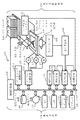
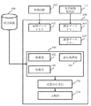
図1は、実施の形態1におけるパターン検査装置の構成を示す概念図である。
図1において、パターンが形成されたマスクやウェハ等の基板を試料として、かかる試料の欠陥を検査するパターン検査装置100は、光学画像取得部150と制御系回路160を備えている。光学画像取得部150は、XYθテーブル102、光源103、拡大光学系104、ラインセンサ105、センサ回路106、レーザ測長システム122、オートローダ130、照明光学系170を備えている。制御系回路160では、コンピュータとなる制御計算機110が、データ伝送路となるバス120を介して、位置回路107、比較回路108、展開回路111、参照回路112、オートローダ制御回路113、テーブル制御回路114、記憶装置の一例となる磁気ディスク装置109、磁気テープ装置115、フレシキブルディスク装置(FD)116、CRT117、パターンモニタ118、プリンタ119に接続されている。また、XYθテーブル102は、X軸モータ、Y軸モータ、θ軸モータにより駆動される。フォトマスク101のパターン形成時に用いた設計データの情報は、磁気ディスク装置109に格納される。また、ここでは、ラインセンサ105は、例えば、フォトダイオードアレイを用いて2画素以上を同時期に検出することができるように構成されている。例えば、2画素以上で構成されるラインセンサを2段以上用いた時間遅延積分センサ(TDIセンサ:タイムディレイインテグレーションセンサ)を用いると好適である。ここでは、例えば、1ラインが2048画素のTDIセンサを用いる。図1では、本実施の形態1を説明する上で必要な構成部分以外については記載を省略している。パターン検査装置100にとって、通常、必要なその他の構成が含まれることは言うまでもない。
FIG. 1 is a conceptual diagram showing the configuration of the pattern inspection apparatus according to the first embodiment.
In FIG. 1, a
図2は、実施の形態1におけるパターン検査方法の要部工程を示すフローチャート図である。
図2において、パターン検査方法は、補正係数取得工程(S102)、光学画像取得工程(S104)と、参照画像作成工程(S106)と、入力&記憶工程(S108)と、偽像成分補正工程(S110)と、比較工程(S112)という一連の工程を実施する。補正係数取得工程(S102)は、実際のパターン検査の事前に実施しておく。
FIG. 2 is a flowchart showing main steps of the pattern inspection method according to the first embodiment.
In FIG. 2, the pattern inspection method includes a correction coefficient acquisition step (S102), an optical image acquisition step (S104), a reference image creation step (S106), an input & storage step (S108), and a false image component correction step ( A series of steps of S110) and a comparison step (S112) are performed. The correction coefficient acquisition step (S102) is performed in advance of actual pattern inspection.
S(ステップ)102において、補正係数取得工程として、実際のパターン検査の準備段階として、偽像成分を補正する補正係数を取得する。詳細については後述する。 In S (step) 102, as a correction coefficient acquisition step, a correction coefficient for correcting the false image component is acquired as an actual pattern inspection preparation stage. Details will be described later.
S104において、光学画像取得工程として、光学画像取得部150は、パターンが形成されたフォトマスク101における光学画像(測定データ)を取得する。具体的には、光学画像は、次のように取得される。被検査試料となるフォトマスク101は、XYθ各軸のモータによって水平方向及び回転方向に移動可能に設けられたXYθテーブル102上に載置され、フォトマスク101に形成されたパターンには、XYθテーブル102の上方に配置されている適切な光源103によって光が照射される。光源103から照射される光束は、照明光学系170を介して試料となるフォトマスク101を照射する。フォトマスク101の下方には、拡大光学系104、ラインセンサ105及びセンサ回路106が配置されており、露光用マスクなどの試料となるフォトマスク101を透過した光は拡大光学系104を介して、ラインセンサ105に光学像として結像し、入射する。拡大光学系104は図示しない自動焦点機構により自動的に焦点調整がなされていてもよい。このようにして、複数のフォトダイオードを有するラインセンサ105を使って、パターン形成されたフォトマスク101の光学画像中の複数の画素情報を同時期に検出する。フォトダイオードは、画素検出部の一例となる。
In S104, as an optical image acquisition step, the optical
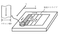
図3は、実施の形態1における光学画像の取得手順を説明するための概念図である。
被検査領域は、図3に示すように、Y方向に向かって、スキャン幅Wの短冊状の複数の検査ストライプに仮想的に分割され、更にその分割された各検査ストライプが連続的に走査されるようにXYθテーブル102の動作が制御され、X方向に移動しながら光学画像が取得される。ラインセンサ105では、図3に示されるようなスキャン幅Wの画像を連続的に入力する。そして、第1の検査ストライプにおける画像を取得した後、第2の検査ストライプにおける画像を今度は逆方向に移動しながら同様にスキャン幅Wの画像を連続的に入力する。そして、第3の検査ストライプにおける画像を取得する場合には、第2の検査ストライプにおける画像を取得する方向とは逆方向、すなわち、第1の検査ストライプにおける画像を取得した方向に移動しながら画像を取得する。このように、連続的に画像を取得していくことで、無駄な処理時間を短縮することができる。例えば、ラインセンサ105に2048画素分のフォトダイオードが配置されているものを用いると、スキャン幅Wは2048画素となる。
FIG. 3 is a conceptual diagram for explaining an optical image acquisition procedure according to the first embodiment.
As shown in FIG. 3, the inspection area is virtually divided into a plurality of strip-shaped inspection stripes having a scan width W in the Y direction, and each of the divided inspection stripes is continuously scanned. Thus, the operation of the XYθ table 102 is controlled, and an optical image is acquired while moving in the X direction. The
ラインセンサ105上に結像されたパターンの像は、ラインセンサ105の各フォトダイオードによって光電変換され、更にセンサ回路106によってA/D(アナログデジタル)変換される。ステージとなるXYθテーブル102をX軸方向に連続的に移動させることにより、ラインセンサ105はフォトマスク101のパターンを撮像する。これらの光源103、拡大光学系104、ラインセンサ105、センサ回路106により高倍率の検査光学系が構成されている。
The pattern image formed on the
XYθテーブル102は、制御計算機110の制御の下にテーブル制御回路114により駆動される。X方向、Y方向、θ方向に駆動する3軸(X−Y−θ)モータの様な駆動系によって移動可能となっている。これらの、Xモータ、Yモータ、θモータは、例えばステップモータを用いることができる。そして、XYθテーブル102の移動位置はレーザ測長システム122により測定され、位置回路107に供給される。また、XYθテーブル102上のフォトマスク101はオートローダ制御回路113により駆動されるオートローダ130から自動的に搬送され、検査終了後に自動的に排出されるものとなっている。
The XYθ table 102 is driven by the
センサ回路106から出力された測定データ(光学画像)は、位置回路107から出力されたXYθテーブル102上におけるフォトマスク101の位置を示すデータとともに比較回路108に送られる。測定データは例えば8ビットの符号なしデータであり、各画素の明るさの階調を表現している。測定データは、例えば、512画素×512画素の画像データ毎に区分けされ、その内部の画素毎に比較される。
Measurement data (optical image) output from the
S106において、参照画像作成工程として、まず、展開回路111は、磁気ディスク装置109から制御計算機110を通して設計データを読み出す。そして、読み出されたフォトマスク101の設計データを2値ないしは多値のイメージデータに変換して、このイメージデータが参照回路112に送られる。
In S <b> 106, as a reference image creation process, first, the
図4は、実施の形態1における展開回路の構成の一例を示す概念図である。
図4において、展開回路111は、階層構造展開回路202、調停回路204、パターン発生回路206、パターンメモリ208、パターン読み出し回路210を有している。そして、パターン発生回路206とパターンメモリ208とで1つの組となって、複数段配置されている。
FIG. 4 is a conceptual diagram showing an example of the configuration of the development circuit in the first embodiment.
4, the
ここで、設計データに含まれる図形は長方形や三角形を基本図形としたもので、例えば、図形の基準位置における座標(x、y)、辺の長さ、長方形や三角形等の図形種を区別する識別子となる図形コードといった情報で各パターン図形の形、大きさ、位置等を定義した図形データが格納されている。かかる図形データの情報が展開回路111に入力されると、階層構造展開回路202は、図形ごとのデータにまで展開し、その図形データの図形形状を示す図形コード、図形寸法などを解釈する。そして、パターン発生回路206において、所定の量子化寸法のグリッドを単位とするマス目内に配置されるパターンとして2値ないしは多値の設計画像データを展開する。そして、展開された設計画像データは、パターンメモリ208に一時的に蓄積される。言い換えれば、占有率演算部の一例となるパターン発生回路206では、設計データを読み込み、検査領域を所定の寸法を単位とするマス目として仮想分割してできたマス目ごとに設計データにおける図形が占める占有率を演算し、nビットの占有率データをパターンメモリ208に出力する。例えば、1つのマス目を1画素として設定すると好適である。そして、1画素に1/28(=1/256)の分解能を持たせるとすると、画素内に配置されている図形の領域分だけ1/256の小領域を割り付けて画素内の占有率を演算する。そして、8ビットの占有率データとしてパターンメモリ208に出力する。
Here, the figure included in the design data is a basic figure such as a rectangle or a triangle. For example, the coordinates (x, y) at the reference position of the figure, the length of the side, and the figure type such as a rectangle or a triangle are distinguished. The graphic data defining the shape, size, position, etc. of each pattern graphic is stored with information such as a graphic code as an identifier. When such graphic data information is input to the
ここで、効率よく複数のパターン発生回路206で並列処理動作を行なわせるため、調停回路204が、各パターン発生回路206への入力データを配分する。そして、パターン読み出し回路210がパターンメモリ208に記憶された占有率データを読み出す。パターン読み出し回路210では、同一画素内の占有率データが存在すれば、かかる占有率データを加算して読み出す。これにより各画素内の図形占有率(階調値)がわかる。
Here, the
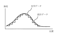
そして、フィルタ処理工程として、参照回路112は、送られてきた図形のイメージデータである設計画像データに適切なフィルタ処理を施す。
図5は、フィルタ処理を説明するための概念図である。
センサ回路106から得られた光学画像としての測定データは、拡大光学系104の解像特性やラインセンサ105のアパーチャ効果等によってフィルタが作用した状態、言い換えれば連続変化するアナログ状態にあるため、画像強度(濃淡値)がデジタル値の設計側のイメージデータである設計画像データにもフィルタ処理を施すことにより、測定データに合わせることができる。このようにして測定データ(光学画像)と比較する参照データ(参照画像)を作成する。そして、作成された参照データは、比較回路108に出力される。
Then, as a filtering process, the
FIG. 5 is a conceptual diagram for explaining the filter processing.
The measurement data as an optical image obtained from the
ここでは、「die to database検査」を行うために設計データに基づいて参照データを作成しているが、これに限るものではない。「die to die検査」を行うこともできる。その場合には、比較対象となる別の測定データ(光学画像)に基づいて参照データを作成すればよい。以上のようにして、測定データを取得し、また、参照データを作成する。次に、上述した補正係数取得工程(S102)の詳細について、図面を用いて説明する。 Here, reference data is created based on design data in order to perform “die to database inspection”, but the present invention is not limited to this. A “die to die inspection” can also be performed. In that case, reference data may be created based on another measurement data (optical image) to be compared. As described above, measurement data is acquired and reference data is created. Next, details of the above-described correction coefficient acquisition step (S102) will be described with reference to the drawings.
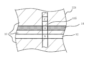
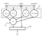
図6は、実施の形態1における補正係数を取得する手法の一例を説明するための概念図である。
まず、図6に示すような、例えば、透明なマスクブランクスの一部の領域を残して残りの領域にクロム(Cr)等を材料とする遮光膜を形成したサンプル基板221を用意する。サンプル基板221には、透過率の低い部分10と所定の幅の透過率の高い部分12とが形成されている。透過率を256階調で表わした場合に、透過率の低い部分10としては、例えば、30階調以下の部分が望ましい。また、透過率の高い部分12としては、例えば、100階調以上の部分が望ましい。このようなパターンをラインセンサ105で撮像するとl番目のフォトダイオードが検出する透過率の高い画素Aの信号aの影響を受けて、画素Aからある距離だけ離れたn番目のフォトダイオードが検出する本来透過率が低いはずの画素Bの信号bが大きな値となってしまう場合がある。すなわち、部分14に位置する画素Bで偽像が生じていることになる。そこで、画素Bの信号bから画素Bと十分離れたp番目のフォトダイオードが検出する画素Cの信号cを引いた差Δ=b−cの絶対値を画素A,B間のクロストークによる成分とする。そして、F_AB=Δ/aをAからBに影響するクロストークの補正係数N(n,l)とする。例えば、画素Cとして画素Bから192画素より離れた画素を用いると好適である。この位離れることで透過率の高い画素Aの信号aの影響を排除することができる。そのため、画素Cの信号cは、本来の透過率が低い場合の値とすることができる。言い換えれば、n番目のフォトダイオードは、l番目のフォトダイオードから例えば192画素分以内の位置関係となる。同様に、その他の位置で検出されるその他の画素についても画素Aの信号aの影響を受けたクロストークの補正係数を演算しておく。さらに、サンプル基板221の位置とラインセンサ105の位置を相対的にずらして、透過率の低い部分10の位置がl番目のフォトダイオード以外のその他の位置になるようにする。例えば、1番目のフォトダイオードの位置とする。そして、同様に、この透過率の低い部分10に位置する画素の信号によるクロストークの補正係数を求める。このようにして、ラインセンサ105上の各フォトダイオードが検出する画素の信号が、その他のフォトダイオードが検出する画素の信号によって影響を受ける補正係数N(n,k)を順次求めておく。補正係数N(n,k)は、例えば、0〜0.01程度となる。ここで、k,l,n,pは、1≦k,l,n,p≦2048であることは言うまでもない。また、補正係数N(n,k)は、上述した方法に限るものではなく、次のような手法で求めても好適である。
FIG. 6 is a conceptual diagram for explaining an example of a technique for acquiring a correction coefficient in the first embodiment.
First, as shown in FIG. 6, for example, a
図7は、実施の形態1における補正係数を取得する手法の他の一例を説明するための概念図である。
まず、図7(a)に示すような、例えば、透明なマスクブランクスの全面領域にクロム(Cr)等を材料とする遮光膜を形成したサンプル基板222を用意する。そして、図7(b)に示すような例えば、透明なマスクブランクスの一部の領域を残して残りの領域にクロム(Cr)等を材料とする遮光膜を形成した図7と同様なサンプル基板221を用意する。サンプル基板221には、透過率の低い部分10と所定の幅の透過率の高い部分12とが形成されている。図7(b)に示すサンプル基板221のパターンをラインセンサ105で撮像すると、上述したようにl番目のフォトダイオードが検出する透過率の高い画素Aの信号aの影響を受けて、画素Aからある距離だけ離れたn番目のフォトダイオードが検出する本来透過率が低いはずの画素Bwの信号bwが大きな値となってしまう場合がある。すなわち、部分14に位置する画素Bwで偽像が生じていることになる。他方、図7(a)に示すサンプル基板222のパターンをラインセンサ105で撮像すると、l番目のフォトダイオードが検出する位置は透過率の低い位置なので画素Aの信号aによって、画素Aからある距離だけ離れたn番目のフォトダイオードが検出する画素Bbの信号bbは、本来の透過率が低い場合の信号となる。そこで、画素Bbの信号bbと画素Bwの信号bwの出力との差Δ=bw−bbの絶対値を用いても同様に、画素A,B間のクロストークの補正係数を求めることができる。同様に、ラインセンサ105上の各フォトダイオードが検出する画素nの信号が、その他のフォトダイオードが検出する画素kの信号によって影響を受ける補正係数N(n,k)を順次求めておく。
FIG. 7 is a conceptual diagram for explaining another example of the method for acquiring the correction coefficient in the first embodiment.
First, as shown in FIG. 7A, for example, a
ここで、上述した各画素の信号は、以下のように取得される。
サンプル基板221は、XYθ各軸のモータによって水平方向及び回転方向に移動可能に設けられたXYθテーブル102上に載置され、サンプル基板221に形成されたパターンには、XYθテーブル102の上方に配置されている適切な光源103によって光が照射される。光源103から照射される光束は、照明光学系170を介してサンプル基板221を照射する。サンプル基板221の下方には、拡大光学系104、ラインセンサ105及びセンサ回路106が配置されており、サンプル基板221を透過した光は拡大光学系104を介して、ラインセンサ105に光学像として結像し、入射する。拡大光学系104は図示しない自動焦点機構により自動的に焦点調整がなされていてもよい。そして、ラインセンサ105上に結像されたパターンの像は、各フォトダイオードによって光電変換され、更にセンサ回路106によってA/D(アナログデジタル)変換される。このようにして各画素の信号を得ることができる。サンプル基板222を用いる場合も同様である。各補正係数N(n,k)は、制御計算機110によって演算されても良いし、その他の演算回路等で求めても構わない。そして、得られた各補正係数N(n,k)は、磁気ディスク装置109に格納しておく。
Here, the signal of each pixel mentioned above is acquired as follows.
The
そして、得られた各補正係数N(n,k)を用いて、上述したように取得された測定データと作成された参照データとを比較して、実際の試料となるパターンが形成されたフォトマスク101のパターン欠陥の有無を検査する。
Then, using the obtained correction coefficients N (n, k), the measurement data acquired as described above is compared with the created reference data, and a photo on which a pattern to be an actual sample is formed is formed. The
図8は、実施の形態1における比較回路の内部構成を示すブロック図である。
図8において、比較回路108は、参照データメモリ302、測定データメモリ304、演算データメモリ330、偽像補正部340、位置合わせ部350、及び比較部360を有している。偽像補正部340は、乗算部342、総和演算部344、及び加算部346を有している。また、比較回路108内で演算されたデータ等は、随時、演算データメモリ330に格納される。また、参照データメモリ302は、参照回路112から入力される参照データを格納する。測定データメモリ304は、光学画像取得部150から入力される測定データを格納する。そして、磁気ディスク装置109には、後述する補正係数が格納されている。
FIG. 8 is a block diagram showing an internal configuration of the comparison circuit according to the first embodiment.
8, the
S108において、入力&記憶工程として、制御計算機110を使って、上述したように例えば512画素×512画素の参照データ毎にデータを読み出して参照データメモリ302に記憶させる。同様に、例えば512画素×512画素の測定データ毎にデータを読み出して測定データメモリ304に記憶させる。
In S <b> 108, as the input & storage step, using the
S110において、偽像成分補正工程として、偽像補正部340は、ラインセンサ105で同時期に検出された複数の画素信号の各画素信号から同時期に検出された複数の画素情報のその他の画素情報に基づく補正量を減ずる補正を行なう。具体的には、以下のように補正を行なう。
In S110, as the false image component correction step, the false
図9は、実施の形態1における偽像成分補正の手法を説明するための概念図である。
図9では、ラインセンサ105で同時期に検出した複数の画素信号における第n番目のフォトダイオードで検出される画素nの画素信号を補正する場合を示している。画素nの画素信号は、その他の画素(画素nを除く1〜2048番目の画素)の画素信号によって、クロストークの影響を受けている可能性がある。そこで、まず、乗算部342は、その他の各画素によって画素nの信号がクロストークの影響を受けた場合の各補正係数N(n,k)をその他の各画素kの信号の画素値に乗算する。すなわち、δk=F×kを計算することにより,画素nに対する画素kからのクロストークによる偽像成分が求まる。そして、総和演算部344は、得られた各値の総和を演算する。すなわち、Σδkを演算する。k=1〜n−1及びn+1〜2048である。この総和が、その他の各画素によって画素nの信号がクロストークの影響を受けた場合の補正量となる。すなわち、補正量は、ラインセンサ105を用いてフォトマスク101の光学画像を検出した際に得られる複数の画素信号の交信により生じる偽像成分を補正する値となる。そして、加算部346が、画素nの信号の画素値から総和値を減ずる演算を行なう。すなわち、画素nの信号n−Σδkを演算する。以上のようにして、画素nの画素信号が、その他の画素の画素信号から受けるクロストークの影響を排除することができる。すなわち、偽像成分を補正することができる。同様にして、n=1〜2048まで各画素の画素信号を補正する。以上のように画素信号の値が補正された各画素情報を使って、参照データの対応する画素信号と比較することになる。
FIG. 9 is a conceptual diagram for explaining a method for correcting a false image component in the first embodiment.
FIG. 9 shows a case where the pixel signal of the pixel n detected by the nth photodiode in a plurality of pixel signals detected at the same time by the
S112において、比較工程として、まず、位置合わせ部350が、各画素信号が補正された測定データと参照データとの位置合わせを行なう。位置合わせは、512×512のフレームサイズの測定データと参照データとについて、各画素の画素値の残差二乗和(SSD:Sum of the Squared Difference)を最小とする位置に合わせる手法や最小二乗法等を用いて演算される位置ずれ量だけずらす手法を適宜用いれば良い。そして、比較部360は、補正された各画素信号と参照データの参照画素信号とを所定のアルゴリズムに従って比較し、欠陥の有無を判定する。そして、比較された結果は出力される。以上のように、クロストークによる偽像成分を除去することで、データ比較の際の欠陥の誤検出を抑制して擬似欠陥を低減することができる。よって、高精度の検査を行うことができる。
In S112, as a comparison process, first, the
実施の形態2.
実施の形態1では、補正係数を求める際に、1ライン全ての画素について補正係数を求めたが、これに限るものではない。実施の形態2では、1ラインを複数のグループに分けてグループ単位で補正係数を算出し,グループ間のクロストークによる偽像を補正する場合について説明する。実施の形態2における装置構成は、図1,8と同様である。また、パターン検査方法の要部工程も図2と同様である。
In the first embodiment, when the correction coefficient is obtained, the correction coefficient is obtained for all the pixels in one line. However, the present invention is not limited to this. In the second embodiment, a case will be described in which one line is divided into a plurality of groups, a correction coefficient is calculated in units of groups, and a false image due to crosstalk between groups is corrected. The apparatus configuration in the second embodiment is the same as that shown in FIGS. Further, the main steps of the pattern inspection method are the same as those in FIG.
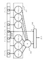
図10は、実施の形態2における偽像成分補正の手法を説明するための概念図である。
図10では、ラインセンサ105における第1番目のフォトダイオードから第2048番目のフォトダイオードを例えば32画素分ずつグループ化する。そして、図10では、各グループをタップa〜タップzとして示している。但し、分割するため際のフォトダイオード数は、これに限るものではない。少なくとも1つのフォトダイオードで構成される複数のグループに分割されればよい。
FIG. 10 is a conceptual diagram for explaining a method for correcting a false image component in the second embodiment.
In FIG. 10, the first to 2048th photodiodes in the
S102において、補正係数取得工程として、まず、偽像成分を補正する補正係数を取得する。実施の形態2では、図6に示すようなパターンをラインセンサ105で撮像する際、透過率の高い部分12の画素を検出することになるタップm内の各フォトダイオードが検出する透過率の高い画素の平均値をタップmの代表値mとする。同様に、偽像が発生する部分14の画素を検出することになるタップn内の各フォトダイオードが検出する画素の平均値をタップnの代表値nとする。同様に、タップnと十分離れた透過率の低い部分10の画素を検出することになるタップp内の各フォトダイオードが検出する透過率の低い画素の平均値をタップpの代表値pとする。そして、タップnの代表値nからタップpの代表値pを引いた差Δ=n−pの絶対値をタップm,n間のクロストークによる成分とする。そして、F_mn=Δ/mをタップmからタップnに影響するクロストークの補正係数N(n,m)とする。例えば、タップpとしてタップnから3タップ分より離れたタップを用いると好適である。同様に、ラインセンサ105上の各タップ内のフォトダイオードが検出する画素の信号が、その他のタップ内フォトダイオードが検出する画素の信号によって影響を受ける補正係数N(n,k)をタップ毎に順次求めておく。補正係数N(n,k)は、例えば、0〜0.01程度となる。このように、補正係数は、グループ毎に設定される値が用いられる。図7に示すようなパターンを使う場合も同様である。そして、S104〜S108の内容は、実施の形態1と同様である。
In S102, as a correction coefficient acquisition step, first, a correction coefficient for correcting a false image component is acquired. In the second embodiment, when the pattern as shown in FIG. 6 is imaged by the
S110において、偽像成分補正工程として、偽像補正部340は、ラインセンサ105で同時期に検出された複数の画素信号の各画素信号から同時期に検出された複数の画素情報のその他の画素情報に基づく補正量を減ずる補正を行なう。具体的には、以下のように補正を行なう。実施の形態2では、その他の画素情報として、各タップ内で検出される少なくとも1つの画素信号に基づく値がタップ毎に代表して用いられる。例えば、タップn内の第k番目の画素の画素信号を補正する場合には、その他のタップ内でも第k番目の画素の画素信号を用いると良い。すなわち、ここでは、32画素分のフォトダイオードで1つのタップのフォトダイオードアレイを構成しているので、隣り合うタップ間では32画素ピッチで検出される画素信号を用いると好適である。図10では、ラインセンサ105で同時期に検出した複数の画素信号における第n番目のタップ内のフォトダイオードで検出される画素nの画素信号を補正する場合を示している。画素nの画素信号は、その他の画素(タップn内の画素nを除く1〜2048番目の画素)の画素信号によって、クロストークの影響を受けている可能性がある。そこで、まず、乗算部342は、その他の各画素によって画素nの信号がクロストークの影響を受けた場合のタップ毎の補正係数N(n,k)をその他の各タップkを代表するタップ内で画素nと同番目の画素となる画素kの信号の画素値に乗算する。すなわち、δk=F×kを計算することにより,画素nに対するタップk内の画素からのクロストークによる偽像成分が求まる。そして、総和演算部344は、得られた各値の総和を演算する。すなわち、Σδkを演算する。k=1〜n−1及びn+1〜zである。この総和が、その他の各タップ内の画素によって画素nの信号がクロストークの影響を受けた場合の補正量となる。そして、加算部346が、画素nの信号の画素値から総和値を減ずる演算を行なう。すなわち、画素nの信号n−Σδkを演算する。以上のようにして、タップn内の画素nの画素信号が、その他のタップ内の画素の画素信号から受けるクロストークの影響を排除することができる。すなわち、偽像成分を補正することができる。同様にして、各タップ内の全画素の画素信号を補正する。そして、S112の内容は、実施の形態1と同様である。
In S110, as the false image component correction step, the false
以上のように、タップ毎に1つの補正量成分を演算することで、偽像成分を補正するための補正量を演算する際の演算時間を大幅に短縮することができる。 As described above, by calculating one correction amount component for each tap, the calculation time for calculating the correction amount for correcting the false image component can be greatly shortened.
実施の形態4.
実施の形態1,2では、検査の準備段階で設定した補正係数を用いて補正量を演算したが、これに限るものではない。実施の形態4では、フォトマスク101の検査中に補正係数を更新する構成について説明する。
Embodiment 4 FIG.
In the first and second embodiments, the correction amount is calculated using the correction coefficient set in the inspection preparation stage, but the present invention is not limited to this. In the fourth embodiment, a configuration in which correction coefficients are updated during inspection of the
図13は、実施の形態4における比較回路の内部構成を示すブロック図である。
図13では、偽像補正部340内にさらに係数演算部368を追加した点以外は、図8と同様である。また、装置全体の構成も図1と同様である。
FIG. 13 is a block diagram illustrating an internal configuration of the comparison circuit according to the fourth embodiment.
13 is the same as FIG. 8 except that a
図14は、実施の形態4におけるパターン検査方法の要部工程を示すフローチャート図である。
図14において、パターン検査方法は、さらに、補正係数演算工程(S105)を追加した点以外は、図2と同様である。
FIG. 14 is a flowchart showing main steps of the pattern inspection method according to the fourth embodiment.
14, the pattern inspection method is the same as that in FIG. 2 except that a correction coefficient calculation step (S105) is further added.
図3において説明したように、フォトマスク101の検査面は、短冊状の複数の検査領域となる複数の検査ストライプに仮想分割され、検査ストライプ毎に順に検査が行われる。そこで、S105において、検査途中であるにも関わらず、偽像補正部340は、事前に検査された検査ストライプで検出された画素信号に基づいて補正係数を演算する。そして、演算された補正係数を元の補正係数に例えば上書きして更新する。但し、フォトマスク101に形成されたパターンは、図6や図7に示したようなパターンとは限らない。そこで、偽像補正部340は、事前に検査された検査ストライプで得られたパターンによって、補正係数を求めることができた箇所についてのみ更新すればよい。補正係数の求め方は、例えば、次のように求めることができる。図7に示すような状態をラインセンサ105で撮像したときと同じ状態であるパターンをラインセンサ105で撮像するとl番目のフォトダイオードが検出する透過率の高い画素Aの信号aの影響を受けて、画素Aからある距離だけ離れたn番目のフォトダイオードが検出する本来透過率が低いはずの画素Bの信号bが大きな値となってしまう場合がある。すなわち、部分14に位置する画素Bで偽像が生じていることになる。ここでは、まず、画素Bの参照データにおける信号b’とn番目のフォトダイオードが検出した画素Bの信号bの差分b”=b’−bを演算する。そして、画素Bと十分離れたp番目のフォトダイオードが検出する画素Cの参照データにおける信号c’とのp番目のフォトダイオードが検出した画素Cの信号cの差分c”=c’−cを演算する。そして、この差分の差Δ=b”−c”の絶対値を画素A,B間のクロストークによる成分とする。そして、F_AB=Δ/aをAからBに影響するクロストークの補正係数N(n,l)とする。このように参照データの値を用いることで欠陥ではなく偽像を補正する補正係数を得ることができる。
As described with reference to FIG. 3, the inspection surface of the
例えば、ラインセンサ105の各出力を常時監視し、透過率の低い部分に対し、近傍に透過率の高い部分が発見された場合に一度検査を中断する。そして、近傍に透過率の高い部分の画素信号によって影響を受ける可能性がある透過率の低い部分の画素に対するクロストーク補正量を算出するための補正係数を計算して更新する。その後、検査を再開することで、ラインセンサ105或いは光源103の経時的変化に対応することができる。その結果、信頼性の高い検査を行うことができる。
For example, each output of the
或いは、次のようなタイミングで更新してもよい。比較部108により比較された結果、欠陥候補となる画素数が所定の閾値を超えた場合に、一度検査を中断する。そして、ユーザにより欠陥候補の内容を確認する。そして、その内容が偽像によるものであると判断された場合に、偽像補正部340は、補正係数を演算する。その場合、偽像が確認された部分を用いて、補正係数を演算すればよい。以上のように、異常な結果が閾値を超えるような出力が成されたときにはラインセンサ105或いは光源103の故障の判定に用いることも実用上有効な手段である。
Alternatively, it may be updated at the following timing. As a result of the comparison by the
ここで、図3において説明したように、パターン検査装置100での検査は、複数の検査ストライプを順方向(FWD方向)と逆方向(BWD方向)の交互動作を繰り返しながら走査することによって行われる。すなわち、XYθテーブル102では、図3に示すようにFWD方向とBWD方向の交互動作をさせる。XYθテーブル102の走行精度によっては、FWD走行時とBWD走行時で特性が若干異なる可能性がある。このような場合に、直前の検査ストライプ、つまりXYθテーブル102が逆方向に動作したときの出力値をもとに補正係数を更新するとかえってずれが大きくなってしまう可能性がある。そこで、補正係数の更新に反映する出力値を同一方向に動作して画像取得した検査ストライプのものを使用する。このように補正係数は、事前に検査された検査ストライプのうち、同方向に走査される検査ストライプで検出された画素信号に基づいて演算されるようにすると好適である。そして、各検査ストライプの各ラインデータに対する偽像を補正する補正係数の平均値を用いるようにするというのも実用的である。例えば、第1検査ストライプがFWD動作であれば、第2検査ストライプはBWD動作、そして第3検査ストライプがFWD動作となるので、第3検査ストライプの補正係数の計算には、第1検査ストライプのセンサ出力結果を反映すると良い。
Here, as described with reference to FIG. 3, the inspection by the
以上のように、ラインセンサ105の並列に読み出している画素間のクロストークを補正するような演算を行えば、クロストークによる偽像を低減することができる。そのために、ラインセンサ105のクロストークの強さを測定することで補正量を演算するためのパラメータを得ることができる。その結果、ラインセンサ105の劣化により偽像が発生しやすくなった場合でも、適当に補正量を変えることにより劣化しても感度をあまり落とすことなく試料の検査を行うことができる。また、ラインセンサ105の劣化に応じて交換時期がわかるシステムとすることができる。
As described above, if a calculation that corrects crosstalk between pixels read in parallel by the
実施の形態5.
以上説明した各実施の形態においては、透過光を利用した検査装置を説明したが、これに限るものではない。
図15は、実施の形態5における反射光を用いたパターン検査装置の構成を示す概念図である。
図15において、光源103と照明光学系170が、拡大光学系104やラインセンサ105側に設けられている点以外は、図1と同様である。図15に示すような反射光を用いたパターン検査装置140であっても同様に用いることができる。或いは、透過光と反射光を同時に用いる装置であってもよい。
Embodiment 5 FIG.
In each of the embodiments described above, the inspection apparatus using transmitted light has been described. However, the present invention is not limited to this.
FIG. 15 is a conceptual diagram showing a configuration of a pattern inspection apparatus using reflected light in the fifth embodiment.
15 is the same as FIG. 1 except that the light source 103 and the illumination optical system 170 are provided on the magnifying
以上の説明において、「〜部」、「〜回路」或いは「〜工程」と記載したものは、コンピュータで動作可能なプログラムにより構成しても構わない。或いは、ソフトウェアとなるプログラムだけではなく、ハードウェアとソフトウェアとの組合せにより実施させても構わない。或いは、ファームウェアとの組合せでも構わない。また、プログラムにより構成される場合、プログラムは、磁気ディスク装置、磁気テープ装置、FD、或いはROM(リードオンリメモリ)等の記録媒体に記録される。例えば、演算制御部を構成するテーブル制御回路114、展開回路111、参照回路112、比較回路108等は、電気的回路で構成されていても良いし、制御計算機110によって処理することのできるソフトウェアとして実現してもよい。また電気的回路とソフトウェアの組み合わせで実現しても良い。
In the above description, what is described as “˜part”, “˜circuit”, or “˜process” may be constituted by a program operable by a computer. Or you may make it implement by not only the program used as software but the combination of hardware and software. Alternatively, a combination with firmware may be used. When configured by a program, the program is recorded on a recording medium such as a magnetic disk device, a magnetic tape device, an FD, or a ROM (Read Only Memory). For example, the
以上、具体例を参照しつつ実施の形態について説明した。しかし、本発明は、これらの具体例に限定されるものではない。 The embodiments have been described above with reference to specific examples. However, the present invention is not limited to these specific examples.
また、装置構成や制御手法等、本発明の説明に直接必要しない部分等については記載を省略したが、必要とされる装置構成や制御手法を適宜選択して用いることができる。 In addition, although descriptions are omitted for parts and the like that are not directly required for the description of the present invention, such as a device configuration and a control method, a required device configuration and a control method can be appropriately selected and used.
その他、本発明の要素を具備し、当業者が適宜設計変更しうる全てのパターン検査装置或いはその方法は、本発明の範囲に包含される。 In addition, all pattern inspection apparatuses or methods that include elements of the present invention and whose design can be changed as appropriate by those skilled in the art are included in the scope of the present invention.
10,12,14 部分
20 補正テーブル
100,140 パターン検査装置
101 フォトマスク
102 XYθテーブル
103 光源
104 拡大光学系
105 ラインセンサ
106 センサ回路
107 位置回路
108 比較回路
109 磁気ディスク装置
110 制御計算機
111 展開回路
112 参照回路
113 オートローダ制御回路
114 テーブル制御回路
115 磁気テープ装置
116 FD
117 CRT
118 パターンモニタ
119 プリンタ
120 バス
122 レーザ測長システム
130 オートローダ
150 光学画像取得部
160 制御系回路
170 照明光学系
221,222 サンプル基板
302 参照データメモリ
304 測定データメモリ
330 演算データメモリ
340,341 偽像補正部
342 乗算部
343 補正値取得部
344 総和演算部
346 加算部
368 係数演算部
350 位置合わせ部
360 比較部
10, 12, 14
117 CRT
118
Claims (6)
同時期に検出された前記複数の画素情報の各画素情報から前記複数の画素情報のその他の画素情報に基づく補正量を減ずる補正を行なう補正部と、
補正された各画素情報と所定の参照画素情報とを比較する比較部と、
を備えたことを特徴とするパターン検査装置。 A sensor having a plurality of pixel detection units that detect a plurality of pixel information in the optical image of the patterned sample to be inspected at the same time;
A correction unit that performs correction to reduce a correction amount based on other pixel information of the plurality of pixel information from each pixel information of the plurality of pixel information detected at the same time;
A comparison unit for comparing each corrected pixel information with predetermined reference pixel information;
A pattern inspection apparatus comprising:
前記その他の画素情報として、各グループ内で検出される少なくとも1つの画素情報に基づく値がグループ毎に代表して用いられ、
前記係数として、グループ毎に設定される値が用いられることを特徴とする請求項2記載のパターン検査装置。 The plurality of pixel detection units are divided into a plurality of groups including at least one pixel detection unit,
As the other pixel information, a value based on at least one pixel information detected in each group is representatively used for each group,
The pattern inspection apparatus according to claim 2, wherein a value set for each group is used as the coefficient.
同時期に検出された前記複数の画素情報の各画素情報から前記複数の画素情報のその他の画素情報に基づく補正量を減ずる補正を行なう補正工程と、
補正された各画素情報と所定の参照画素情報とを比較し、比較結果を出力する比較工程と、
を備えたことを特徴とするパターン検査方法。 Using a sensor having a plurality of pixel detection units, a detection step of detecting a plurality of pieces of pixel information in an optical image of a patterned sample to be inspected at the same time;
A correction step of performing correction to reduce a correction amount based on other pixel information of the plurality of pixel information from each pixel information of the plurality of pixel information detected at the same time;
A comparison step of comparing each corrected pixel information with predetermined reference pixel information and outputting a comparison result;
A pattern inspection method comprising:
所定の参照画素情報を第2の記憶装置に記憶する第2の記憶処理と、
前記第1の記憶装置から同時期に検出された前記複数の画素情報を読み出し、前記複数の画素情報の各画素情報から前記複数の画素情報のその他の画素情報に基づく補正量を減ずる補正を行なう補正処理と、
前記第2の記憶装置から所定の参照画素情報を読み出し、補正された各画素情報と前記所定の参照画素情報とを比較し、比較結果を出力する比較処理と、
をコンピュータに実行させるためのプログラム。 A first storage process for storing, in a first storage device, a plurality of pixel information in an optical image of a patterned sample to be inspected detected at the same time using a sensor having a plurality of pixel detection units;
A second storage process for storing predetermined reference pixel information in a second storage device;
The plurality of pieces of pixel information detected at the same time are read from the first storage device, and correction is performed by subtracting a correction amount based on the other pieces of pixel information of the plurality of pieces of pixel information from each piece of pixel information of the plurality of pieces of pixel information. Correction processing,
A comparison process of reading predetermined reference pixel information from the second storage device, comparing each corrected pixel information with the predetermined reference pixel information, and outputting a comparison result;
A program that causes a computer to execute.
Priority Applications (1)
| Application Number | Priority Date | Filing Date | Title |
|---|---|---|---|
| JP2007075962A JP4554635B2 (en) | 2007-03-23 | 2007-03-23 | Pattern inspection apparatus, pattern inspection method, and program |
Applications Claiming Priority (1)
| Application Number | Priority Date | Filing Date | Title |
|---|---|---|---|
| JP2007075962A JP4554635B2 (en) | 2007-03-23 | 2007-03-23 | Pattern inspection apparatus, pattern inspection method, and program |
Publications (2)
| Publication Number | Publication Date |
|---|---|
| JP2008233723A JP2008233723A (en) | 2008-10-02 |
| JP4554635B2 true JP4554635B2 (en) | 2010-09-29 |
Family
ID=39906548
Family Applications (1)
| Application Number | Title | Priority Date | Filing Date |
|---|---|---|---|
| JP2007075962A Active JP4554635B2 (en) | 2007-03-23 | 2007-03-23 | Pattern inspection apparatus, pattern inspection method, and program |
Country Status (1)
| Country | Link |
|---|---|
| JP (1) | JP4554635B2 (en) |
Families Citing this family (1)
| Publication number | Priority date | Publication date | Assignee | Title |
|---|---|---|---|---|
| JP7442375B2 (en) * | 2020-04-06 | 2024-03-04 | 株式会社ニューフレアテクノロジー | Multi-electron beam inspection device and multi-electron beam inspection method |
Family Cites Families (2)
| Publication number | Priority date | Publication date | Assignee | Title |
|---|---|---|---|---|
| JPH03129974A (en) * | 1989-10-13 | 1991-06-03 | Ricoh Co Ltd | Offset voltage reduction circuit |
| JPH10200709A (en) * | 1997-01-07 | 1998-07-31 | Nikon Corp | Brightness / darkness information reading method and apparatus therefor |
-
2007
- 2007-03-23 JP JP2007075962A patent/JP4554635B2/en active Active
Also Published As
| Publication number | Publication date |
|---|---|
| JP2008233723A (en) | 2008-10-02 |
Similar Documents
| Publication | Publication Date | Title |
|---|---|---|
| JP5753461B2 (en) | Pattern inspection apparatus and pattern inspection method | |
| US8260031B2 (en) | Pattern inspection apparatus, pattern inspection method, and computer-readable recording medium storing a program | |
| JP6132658B2 (en) | Inspection sensitivity evaluation method | |
| US10460435B2 (en) | Pattern inspection method and pattern inspection apparatus | |
| JP5305641B2 (en) | Pattern inspection apparatus and pattern inspection method | |
| KR101994524B1 (en) | Focusing device, focusing method, and pattern inspection method | |
| JP6310263B2 (en) | Inspection device | |
| JP6633918B2 (en) | Pattern inspection equipment | |
| JP4174504B2 (en) | Sample inspection apparatus, sample inspection method, and program | |
| JP5514754B2 (en) | Inspection apparatus and inspection method | |
| JP5178781B2 (en) | Sensor output data correction device and sensor output data correction method | |
| US8442320B2 (en) | Pattern inspection apparatus and pattern inspection method | |
| JP4185516B2 (en) | Sample inspection apparatus, sample inspection method, and program | |
| JP4448181B2 (en) | Pattern inspection method, pattern inspection apparatus, and program | |
| JP5010701B2 (en) | Inspection apparatus and inspection method | |
| JP5684628B2 (en) | Pattern inspection apparatus and pattern inspection method | |
| JP4554635B2 (en) | Pattern inspection apparatus, pattern inspection method, and program | |
| JP3958328B2 (en) | Sample inspection apparatus, sample inspection method, and program | |
| JP4772815B2 (en) | Correction pattern image generation apparatus, pattern inspection apparatus, and correction pattern image generation method | |
| JP7751504B2 (en) | Pattern inspection method and pattern inspection device | |
| JP4554661B2 (en) | Pattern inspection apparatus, pattern inspection method, and program | |
| JP2016035539A (en) | Position measurement method, method for creating map of positional deviation, and inspection system | |
| JP4960404B2 (en) | Pattern inspection apparatus and pattern inspection method | |
| JP4131728B2 (en) | Image creation method, image creation apparatus, and pattern inspection apparatus | |
| JP4922381B2 (en) | Pattern inspection apparatus and pattern inspection method |
Legal Events
| Date | Code | Title | Description |
|---|---|---|---|
| A131 | Notification of reasons for refusal |
Free format text: JAPANESE INTERMEDIATE CODE: A131 Effective date: 20100406 |
|
| A521 | Request for written amendment filed |
Free format text: JAPANESE INTERMEDIATE CODE: A523 Effective date: 20100524 |
|
| TRDD | Decision of grant or rejection written | ||
| A01 | Written decision to grant a patent or to grant a registration (utility model) |
Free format text: JAPANESE INTERMEDIATE CODE: A01 Effective date: 20100615 |
|
| A01 | Written decision to grant a patent or to grant a registration (utility model) |
Free format text: JAPANESE INTERMEDIATE CODE: A01 |
|
| A61 | First payment of annual fees (during grant procedure) |
Free format text: JAPANESE INTERMEDIATE CODE: A61 Effective date: 20100714 |
|
| FPAY | Renewal fee payment (event date is renewal date of database) |
Free format text: PAYMENT UNTIL: 20130723 Year of fee payment: 3 |
|
| R150 | Certificate of patent or registration of utility model |
Ref document number: 4554635 Country of ref document: JP Free format text: JAPANESE INTERMEDIATE CODE: R150 Free format text: JAPANESE INTERMEDIATE CODE: R150 |
|
| FPAY | Renewal fee payment (event date is renewal date of database) |
Free format text: PAYMENT UNTIL: 20130723 Year of fee payment: 3 |
|
| S111 | Request for change of ownership or part of ownership |
Free format text: JAPANESE INTERMEDIATE CODE: R313113 |
|
| FPAY | Renewal fee payment (event date is renewal date of database) |
Free format text: PAYMENT UNTIL: 20130723 Year of fee payment: 3 |
|
| R360 | Written notification for declining of transfer of rights |
Free format text: JAPANESE INTERMEDIATE CODE: R360 |
|
| FPAY | Renewal fee payment (event date is renewal date of database) |
Free format text: PAYMENT UNTIL: 20130723 Year of fee payment: 3 |
|
| R360 | Written notification for declining of transfer of rights |
Free format text: JAPANESE INTERMEDIATE CODE: R360 |
|
| R371 | Transfer withdrawn |
Free format text: JAPANESE INTERMEDIATE CODE: R371 |
|
| FPAY | Renewal fee payment (event date is renewal date of database) |
Free format text: PAYMENT UNTIL: 20130723 Year of fee payment: 3 |
|
| S111 | Request for change of ownership or part of ownership |
Free format text: JAPANESE INTERMEDIATE CODE: R313113 |
|
| FPAY | Renewal fee payment (event date is renewal date of database) |
Free format text: PAYMENT UNTIL: 20130723 Year of fee payment: 3 |
|
| R350 | Written notification of registration of transfer |
Free format text: JAPANESE INTERMEDIATE CODE: R350 |
|
| S111 | Request for change of ownership or part of ownership |
Free format text: JAPANESE INTERMEDIATE CODE: R313115 |
|
| R350 | Written notification of registration of transfer |
Free format text: JAPANESE INTERMEDIATE CODE: R350 |
|
| S111 | Request for change of ownership or part of ownership |
Free format text: JAPANESE INTERMEDIATE CODE: R313115 |
|
| R350 | Written notification of registration of transfer |
Free format text: JAPANESE INTERMEDIATE CODE: R350 |