JP4552257B2 - Lighting device - Google Patents
Lighting device Download PDFInfo
- Publication number
- JP4552257B2 JP4552257B2 JP2000077796A JP2000077796A JP4552257B2 JP 4552257 B2 JP4552257 B2 JP 4552257B2 JP 2000077796 A JP2000077796 A JP 2000077796A JP 2000077796 A JP2000077796 A JP 2000077796A JP 4552257 B2 JP4552257 B2 JP 4552257B2
- Authority
- JP
- Japan
- Prior art keywords
- light
- light emitting
- ultraviolet
- liquid crystal
- visible light
- Prior art date
- Legal status (The legal status is an assumption and is not a legal conclusion. Google has not performed a legal analysis and makes no representation as to the accuracy of the status listed.)
- Expired - Fee Related
Links
Images
Landscapes
- Liquid Crystal (AREA)
- Transforming Electric Information Into Light Information (AREA)
- Non-Portable Lighting Devices Or Systems Thereof (AREA)
- Planar Illumination Modules (AREA)
Description
【0001】
【発明の属する技術分野】
本発明は、例えば液晶ディスプレイのバックライトとして好適な照明装置に関する。
【0002】
【従来の技術】
近年、設置スペースや携帯性を考慮して薄型で構成されたテレビジョン受像機や、コンピュータ装置用のディスプレイが普及してきている。そして、これらの薄型ディスプレイとしては例えば液晶パネルを用いた液晶ディスプレイがよく知られている。
【0003】
ところで、透過型の液晶ディスプレイは、液晶パネルに対して光を照射するためのバックライトが必要とされる。このため、液晶ディスプレイの種類としては、バックライトを液晶パネルの直下に配置したタイプ(以下、「直下型液晶ディスプレイ」という)と、バックライトを液晶パネルの下方側面に配置したタイプ(以下、「エッジライト型液晶ディスプレイ」という)とに大別することができる。
【0004】
以下、図8〜図12を参照しながら従来の液晶ディスプレイに備えられているバックライトの構成について説明する。
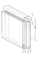
図8は従来の直下型液晶ディスプレイに備えられているバックライトの構成を説明するための斜視図、図9はその断面図である。
この図8、図9に示すように、直下型液晶ディスプレイ100のバックライトは、棒状の形状とされる複数本の蛍光管101と、これら蛍光管101から出射された光線(主に可視光線)105を液晶パネル104側(光出射側)に反射させる反射板102と、液晶パネル104の手前に配置され、複数本の蛍光管101による光源の輝度ムラを目立たせないようにするための拡散板103とにより構成される。
【0005】
ここで、図10に蛍光管の一例としてよく知られている熱陰極管の構造を示す。
この図10に示すように、蛍光管101はガラス管115の外側で、その左右両端に一対の口金ピン111,111が設けられている。そして、この口金ピン111,111に電圧をかけるとガラス管115内の電極112が暖められ、電極112から熱電子が放出される。そして、この口金ピン111に対して交流或いは直流の高電圧をかけることで電極112,112間を放電させるようにする。すると、この放電によってガラス管115内に封止されている水銀蒸気113が励起されて、ガラス管内に紫外線が発生し、さらにこの紫外線がガラス管115の内面側に塗布されている蛍光体114を励起して可視光線が発生する。そして、この可視光線がガラス管115を通してその外部に出射されることになる。
【0006】
従って、図9に示す直下型液晶ディスプレイでは、蛍光管101から出射された可視光線105が、直接、或いは反射板102で反射して拡散板103に照射される。この時、蛍光管101から拡散板103に到達する可視光線105には、蛍光管101が空間的に離散的な位置に配置されているなどの理由によりムラが生じているが、可視光線105は拡散板103により拡散されるので液晶パネル104に照射される光束の均一化が図られている。
【0007】
また、図11は従来のエッジライト型液晶ディスプレイに備えられているバックライトの構成を説明するための斜視図、図12はその断面図である。なお、上記図8、図9に示した直下型液晶ディスプレイと同一部位には同一番号を付し説明は省略する。
【0008】
この図11、図12に示すエッジライト型液晶ディスプレイ120のバックライトは、光源として1つの蛍光管101が液晶パネル104の下方側面に配置されている。この場合、蛍光管101から出射された可視光線105を液晶パネル104の下方側に反射する反射板121と、蛍光管101からの可視光線105を拡散板103を通して液晶パネル104全体に導くための導光体122と、導光体122を通る光を反射する反射板102が設けられている。
【0009】
この場合、蛍光管101から出射された可視光線105は、図12に示すように、直接、或いは反射板121で反射されて導光体122に入射される。この時、導光体122に入射された光線の一部は導光体122の上部界面から出射されるが、導光体122から上部空間への入射角(θ)が臨界角以上とされる光線は界面で反射される。
【0010】
そして、反射された可視光線105は、導光体122の下面側の反射板102によって全反射されて再び上面方向へ進み、その一部が導光体122の上部界面から出射される。このように可視光線105が導光体122内で反射を繰り返すことで、導光体122の上部から出射された光が拡散板103全体を照射するようにされる。この場合も、導光体122から拡散板103に照射される可視光線105には輝度ムラが生じることになるが、上記同様、拡散板103により拡散させることで液晶パネル104に照射される光束の均一化が図られている。
【0011】
【発明が解決しようとする課題】
ところが、上記したような直下型液晶ディスプレイ100、或いはエッジライト型液晶ディスプレイにおいては、光源として蛍光管101を使用しているため、後述するような要因により液晶パネル104に照射される可視光線105の照度が減り、結果として液晶パネル104に映し出される映像の輝度が低下するという問題が有る。
【0012】
上記した問題点を直下型液晶ディスプレイを例に挙げて説明する。
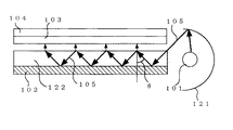
図13は、先に図9に示した直下型液晶ディスプレイの断面図の一部を拡大して示した図である。
先においても説明したが、蛍光管101は、図13に示すように、ガラス管115の内部で発生した紫外線116が蛍光体114を励起して、その外部に可視光線105を出射する構造となっている。このような構造とされる場合は、ガラス管115の内面に塗布されている蛍光体114を通過する際に減衰し、出射される可視光線105に損失が生じる。
【0013】
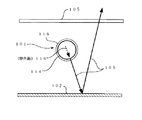
ここで、図14に示す蛍光管101のガラス管115と蛍光体114の部分の拡大図を参照しながら可視光線105に損失が生じる要因について具体的に説明する。
この図14に示す矢印Aは、蛍光管101から出射される可視光線105の観測方向(光出射方向)を示している。
ガラス管115に塗布されている蛍光体114は、点線で示した紫外線116及び実線で示した可視光線105を透過しにくい性質を有している。このため、蛍光管101の内部で発生した紫外線116と紫外線116により発生した可視光線105が蛍光体114の内部で減衰する。
【0014】
そこで、先ず、蛍光体114において発生する紫外線116の減衰について説明する。
先ず、蛍光体114の膜厚を有限(図中厚みをLで示す)とすると、蛍光管101の内部で発生した紫外線116は蛍光体114に照射されるが、この場合、紫外線116の全てが蛍光体114に浸透することなく蛍光体114で変換される可視光線105は、蛍光体114の表面側(内壁側)の位置mで多く深面側(ガラス管115側)の位置kで少なくなる。
【0015】
ここで、例えば図14に示す蛍光体114の位置mに照射される紫外線116の紫外線量をU、また蛍光体114により減衰する紫外線量Uが蛍光体114の膜厚に比例するものとし、例えばその膜厚Lの蛍光体114における紫外線116の損失をそれぞれ80%とする。
【0016】
この場合、蛍光体114の位置kにおける紫外線量は0.2×Uとなり、中間位置iにおける紫外線量は0.6×Uとなる。
従って、蛍光体114の各位置m,i,kにおける可視光線量を、それぞれB1,B2,B3とすれば、B2とB1の関係及びB3とB1との関係は、
B2=0.6×B1・・・(式1)
B3=0.2×B1・・・(式2)
と示すことができる。
【0017】
また、蛍光体114の各位置m,i,kにおいて発光した可視光線105も蛍光体114を通過する際に減衰するものとし、例えば蛍光体114における可視光線105の減衰量を、上記紫外線116と同様、蛍光体114の膜厚に比例するものとし、例えば膜厚Lにおける可視光線105の損失を上記紫外線116と同様、80%とする。
さらに、ガラス管115の可視光線105の透過率を100%とすると、
観測方向Aから観測される光束(可視光線量)Bは、
B=(B1×0.2)+(B2×0.6)+(B3×1.0)・・(式3)
となる。
【0018】
従って、上記(式1)、(式2)を(式3)に代入し、蛍光体114の内壁面側の位置mにおいて発生する可視光線量B1に対する蛍光体114の外面側の位置kにおいて観測される光束Bは、
B=0.76×B1・・・(式4)
となる。即ち、蛍光管101から出射される可視光線105の光束Bは、蛍光管101に塗布されている蛍光体114の表面で発生する可視光線量B1の76%となことが分かる。
【0019】
このように直下型液晶ディスプレイの光源として蛍光管101を使用した場合は、蛍光体114の厚みLによる光透過損失によって、蛍光体114の表面で発生する可視光線量B1の約24%が減衰し、結果として液晶パネル104に映し出される映像の輝度が低下するという問題点があった。
【0020】
特に、従来の直下型液晶ディスプレイ100では、図15に示すように蛍光管101から出射された可視光線105は、直接或いは反射板102を介して拡散板103に照射されるが、反射板102により反射した可視光線105の一部は、図示するように、再び蛍光管101を通って拡散板103に照射されることになる。この時、再び蛍光管101を通過して拡散板103に照射される光束Bは、蛍光管101に塗布されている蛍光体114により減衰され、蛍光管101から直接、拡散板103に照射される光束よりも少なくなる。この結果、拡散板103に照射される光束にムラが生じて液晶パネル104の表面に輝度ムラが生じるという問題点もあった。
【0021】
そこで、従来の直下型液晶ディスプレイ100では、液晶パネル104における輝度ムラの低減を図るため、例えば拡散板103の拡散率を大きくするといったことが行われているが、拡散板103の拡散率を大きくした場合は拡散板103の透過率の低下を招き、結果として液晶パネル104上での輝度低下が大きくなってしまうという問題点が発生する。
【0022】
【課題を解決するための手段】
本発明は、上記したような問題点を解決するためになされたもので、少なくとも紫外線を含む光を放出する光源と、紫外線を可視光線に変換して発光する発光手段と、少なくとも、可視光線を透過し、紫外線を反射するフィルタ手段とを備え、光源から出射される紫外線を封じ込めるようにフィルタ手段と発光手段と対向配置すると共に、フィルタ手段が可視光線の光出射側となるように配置するようにした。
【0023】
さらに、上記発光手段の上記光源とは反対側の面に、紫外線及び可視光線を反射する反射手段を設けるようにした。
【0024】
本発明によれば、フィルタ手段と発光手段を光源を挟んで対向配置して、光源から放出される紫外線を封じ込めるようにしているため、紫外線の殆どが直接或いはフィルタ手段で反射して発光手段に照射されるので発光手段で効率よく紫外線を可視光線に変換することができる。また、発光手段の上記光源とは反対側の面にフィルタ手段を配置することでさらに効率よく発光手段から可視光線を出射させることができる。
【0025】
【発明の実施の形態】
以下、本発明の照明装置の実施の形態について説明する。
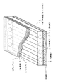
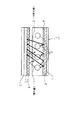
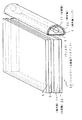
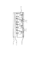
図1、図2は本発明の実施の形態とされる直下型液晶ディスプレイのバックライトの構造を説明するための図であり、図1はその斜視図、図2はその断面図である。
この図1、図2に示す直下型液晶ディスプレイ1は、少なくとも点線で示した紫外線11を含む光を出射する複数本の放電ランプ(紫外線ランプ)2と、紫外線11が照射されると可視光線12を発光する発光板3と、紫外線を反射すると共に可視光線12を透過させ、さらに赤外線を吸収または反射するフィルタ4と、このフィルタ4の上面側(光出射側)に複数本の紫外線ランプ2による光源のムラを目立たせないようにするための拡散板5とが設けられている。
さらに、紫外線ランプ2を介して液晶パネル6とは反対側の位置(下面側)に発光板3が配置され、この発光板3の上に保護膜8がコーティングされている。
また、発光板3の下面には紫外線11及び可視光線12を反射する反射板7が設けられている。
【0026】
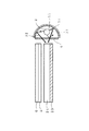
紫外線ランプ2は、例えば上記した蛍光管101と同様、棒状の形状とされる。例えば紫外線ランプ2を熱陰極管或いは冷陰極管により構成する場合は、その内部に水銀蒸気を封入することで紫外線を発生させることができる。この場合、放電によって発生する水銀のスペクトル中の紫外線は、253.7nmの共鳴放射が最も強くなる。
なお、水銀蒸気を封じ込めるためのガラスチューブ(ガラス管)は、紫外線11と可視光線12の減衰を最小限にするため、例えば紫外線11の波長領域(100nm〜380nm)と、可視光線12の波長領域(400nm〜700nm)の光を透過する例えば石英ガラス等の材質で構成されている。
【0027】
発光板3は、紫外線ランプ2から出射される紫外線11を可視光線12に変換する。このため、発光板3は紫外線11を可視光線12に変換する蛍光膜によって形成されている。
蛍光体の材料としては、例えば商品名「NP−105:B(SrCaBa)5(PO4)3Cl:Eu」、「NP−220:G(LaPO4:CeTb)」、「NP−340:R(Y2O3:Eu)」:日亜化学製が用いられ、例えばその調合比率は、R:G:B=33:24:44とすれば良い。
【0028】
また、発光板3の表面側にコーティングが施されている保護膜8は、例えば紫外線11と可視光線12を透過する透過部材とされる。
保護膜8の具体的な材料としては、例えばSiO2やMgO等が挙げられるが、紫外線11と可視光線12を透過できればこの限りではない。
また、発光板3の下に形成されている反射板7は、例えば紫外線11及び可視光線12を反射する反射部材をコーティング、または貼り付けることによって形成される。反射板7の材質としては、例えば銀蒸着等が考えられるが、紫外線11及び可視光線12を反射できればこの限りではない。
【0029】
フィルタ4は、後述するように、紫外線11を反射すると共に可視光線12を透過するフィルタとされる。さらに赤外線を吸収または反射する作用を有するものとされる。
【0030】
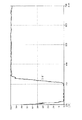
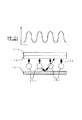
図5はフィルタ4の特性の一例を示した図である。
この図5に示すようにフィルタ4は、紫外線11の波長領域とされる100nm〜380nmの光をほぼ完全に遮断して反射すると共に、波長領域が400nm以上とされる可視光線12を通過させるような特性を有している。
従って、例えば紫外線ランプ2から最も強く出射される253.7nmの紫外線11は、このフィルタ4により反射されて発光板3に照射され、発光板3にて可視光線12に変換される。
なお、フィルタ4は例えば多層薄膜を用いた干渉膜フィルタなどによって構成することが可能とされるが、上述したような特性を持てばこの限りではない。
【0031】
このように本実施の形態とされる直下型液晶ディスプレイ1のバックライトは、従来、光源として用いていた蛍光管101の代わりに紫外線を出射する紫外線ランプ2を用いると共に、この紫外線ランプ2から出射される紫外線11を可視光線12に変換する発光板3を紫外線ランプ2の下面に配置する。そして、紫外線ランプ2の上面に、少なくとも紫外線11を反射し、可視光線12を透過させるフィルタ4を配置するようにしている。
つまり、紫外線ランプ2から出射される紫外線11を封じ込めると共に、フィルタ4が可視光線12の出射側となるように、紫外線ランプ2を挟んでフィルタ4と発光板3とが対向配置されている。
【0032】
この場合、図2に示すように、紫外線ランプ2から出射された紫外線11は、直接、或いはフィルタ4で反射して発光板3に照射され、発光板3で可視光線12が発生する。そして、この可視光線12だけがフィルタ4を透過して光出射側に配置されている拡散板5に達する。そして、拡散板5により液晶パネル6に照射される光束の均一化を図るようにしている。
【0033】
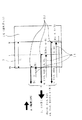
ここで、上記図1、図2に示したバックライトにおける紫外線11の可視光線12への変換について図3を参照しながら具体的に説明する。
本実施の形態では、発光板3を光源とされる紫外線ランプ2の外部で紫外線ランプ2の下面側に配置しているため、可視光線12の観測方向A、即ち液晶パネル6の配置方向である光出射方向が、上記図14とは異なり発光板3に入射する紫外線11の入射方向と同一となる。
なお、発光板3の蛍光体は、上記図14に示した蛍光体114と同一材料とし、紫外線11及び可視光線12を透過しにくい性質を有しているものとする。
従って、紫外線11及び可視光線12は発光板3の蛍光体により減衰するものとされる。
なお、説明を分かり易くするため、ここでは発光板3の下面側に取り付けられている反射板7による影響は考慮しないものとする。
【0034】
ここで、上記発光板3の蛍光体の厚みをLとし、紫外線ランプ2で発生した紫外線11は発光板3に照射されるが、この場合も上記図14と同様、紫外線11が発光板3の蛍光体に浸透しにくいため発光板3で変換される可視光線12は、蛍光体114の表面側の位置mで多く深面側の位置kで少なくなる。
また、例えば発光板3の位置mに照射される紫外線量をU、これにより発光板3で発光する可視光線量をBとし、また発光板3によって減衰する紫外線量Uは発光板3の膜厚に比例するものとし、例えば膜厚Lの発光板3における紫外線11の損失をそれぞれ80%とする。
【0035】
この場合も、発光板3の位置kにおける紫外線量は0.2×U、また膜厚Lの中間位置iにおける紫外線量は0.6×Uとなる。
従って、発光板3の各位置m,i,kにおける可視光線量BをそれぞれB1,B2,B3とすれば、B2とB1の関係及びB3とB1との関係は上記した(式1)、(式2)によって示すことができる。
【0036】
また、発光板3で発光した可視光線量Bもまた、上記図14と同様に、発光板3の蛍光体を通過する際に減衰するものとされるが、本実施の形態では、紫外線11の入射方向と観測方向が同一とされることから観測される光束(可視光線量)Bは、
B=(B1×1.0)+(B2×0.6)+(B3×0.2)・・(式5)
と示すことができる。
【0037】
従って、上記(式1)、(式2)を(式5)に代入し、発光板3の位置mにおいて発生する可視光線量B1に対する、位置m点における可視光線量Bは、
B=1.40×B1・・・(式6)
となる。
【0038】
このように本実施の形態では、発光板3を紫外線ランプ2の外部で紫外線ランプ2の下側に配置し、発光板3で発生した可視光線12の出射方向と、発光板3に入射する紫外線11の入射方向が同一方向とすることで、発光板3からは、発光板3の表面で発生する可視光線量B1の1.4倍の可視光線Bが発生することになる。従って、本実施の形態によれば、(式6)と(式4)とを比較すれば明らかなように、従来の約1.9倍の可視光線量Bが得られることになる。
【0039】
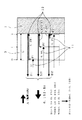
次に、図4を用いて発光板3の下面に設けられている反射板7による可視光線量Bの影響について説明する。
この場合も上記図3と同様、発光板3のそれぞれの位置m,i,kで得られる可視光線量をそれぞれB1,B2,B3とすれば、B2とB1の関係及びB3とB1との関係は、上記(式1)及び(式2)によって表すことができる。
【0040】
そして、これらの発光板3の各位置において変換された可視光線量B1、B2、B3が発光板3の内部を通過し、反射板7で反射して再び観測位置Aに戻った時に観測される各可視光線量をB11,B12,B13とすれば、
B11=0.2×(0.2B1) ・・・(式7)
B22=0.2×(0.6×0.6B1)・・・(式8)
B33=0.2×(0.2B1) ・・・(式9)
と表すことができる。
【0041】
従って、反射板7により増加する可視光線量ΔBは、
ΔB=B11+B22+B33=0.2×0.76B1・・・(式10)
ΔB=0.152×B1・・・(式11)
となる。即ち、発光板3の下面に反射板7を設けることで可視光線量BはΔBだけ増加することになる。
【0042】
さらに本実施の形態では、紫外線ランプ2と拡散板5との間には、可視光線12は透過するものの、紫外線11を反射するフィルタ4を配置することで、発光板3に照射される紫外線11の増加を図るようにしている。
この場合の紫外線11の増加量は、紫外線ランプ2の配置位置などによって決まるが、ここで簡単のため、紫外線ランプ2から出射された紫外線11の半分の内、80%がフィルタ4に到達し、このフィルタ4で紫外線11が90%の反射率で反射し、さらにこの反射した紫外線11の内、80%が発光板3に到達したと仮定する。
するとフィルタ4を配置したことによって発光板3に照射される紫外線11の増加量ΔUは、
ΔU=0.8×0.9×0.8=0.576・・・(式12)
と示される。
即ち、フィルタ4を設けることで、約1.576倍の紫外線11を発光板3に照射することができるため、それだけ発光板3において発生する可視光線12の可視光線量Bを増加することができる。
【0043】
このように、本実施の形態とされる直下型液晶ディスプレイ1では、発光板3を紫外線ランプ2の外側で下面側に配置したことによる可視光線量Bの増加と、発光板3の下面に反射板7を配置したことによる可視光線量Bの増加、及び光出射側に紫外線11を反射するフィルタ4を配置したことによる紫外線量Uの増加という3つの要因によって、液晶パネル6に照射される可視光線量Bの増加を図るようにしている。
【0044】
そして、これらを合わせた総合的な可視光線量Bは、
B=(1.40+0.152)×1.576×B1≒2.5B1・・(式13)
となり、本実施の形態とされる直下型液晶ディスプレイ1のバックライトから出射される可視光線量Bは、従来の液晶ディスプレイのバックライトの可視光線量B(0.76B1)の約3.7倍まで増加することができるものである。
【0045】
なお、本実施の形態における光量の算出方法は、あくまでも便宜的に述べたものであって、厳密に算出する場合は積分等を用いて行う必要があることは言うまでもない。
【0046】
また、本実施の形態では、紫外線ランプ2が紫外線11及び可視光線12を透過するため、フィルタ4で反射された紫外線11や発光板3から発生した可視光線12が紫外線ランプ2を通過した時に殆ど減衰しないものとされる。
従って、拡散板5に照射される可視光線12のムラが小さくなり、拡散板5の拡散率を小さくすることができる。これにより、拡散板5の透過率が大きくなり液晶パネル6に映し出される映像の輝度を向上させることができる。
【0047】
また、フィルタ4は紫外線11を反射するため、紫外線11が拡散板5を介して液晶パネル6に紫外線11が照射されることがなく、液晶パネル6の配向膜が紫外線11によるダメージを受けることがないという利点もある。
さらにフィルタ4に赤外線を反射または吸収することができる部材を用いるようにすれば、赤外線が液晶パネル6に達することもないので、液晶パネル6に対する熱的なストレスも軽減されるという効果もある。
【0048】
また、本発明はこれまで説明した直下型液晶ディスプレイに限定されるものではなく、例えばエッジライト型液晶ディスプレイに適用することも可能とされる。
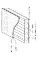
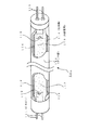
図6、図7は本発明の第2の実施の形態とされるエッジライト型液晶ディスプレイのバックライトの構造を説明するための図であり、図6はその斜視図、図7は断面図である。なお、図1及び図2と同一部位には同一番号を詳細な説明は省略する。
【0049】
この図6、図7に示す液晶ディスプレイ20のバックライトは、光源とされる1つの紫外線ランプ2が液晶パネル6の下方側面に配置されている。そして、この紫外線ランプ2からの紫外線11が照射されると可視光線12を発光する発光板22と、紫外線11を反射すると共に、可視光線12を透過させ、さらに赤外線を吸収または反射するフィルタ4と、可視光線12を拡散板5を通して液晶パネル6全体に導くための導光体24と反射板23が設けられている。
そして、この場合も可視光線12の出射側にフィルタ4が配置されていると共に、紫外線ランプ2を介して液晶パネル6とは反対側に発光板22が配置され、この発光板3の裏面に紫外線11及び可視光線12を反射する反射板21が設けられている。
【0050】
この場合も、図7に示すように、紫外線ランプ2から出射された紫外線11は、直接、或いはフィルタ4で反射して発光板22に照射され、発光板22で可視光線12が発生する。そして、この可視光線12だけが光出射側に配置されているフィルタ4を透過して拡散板5に達する。そして、拡散板5により液晶パネル6に照射される光束の均一化を図るようにしている。
従って、上記図1、図2に示した直下型液晶ディスプレイと同様の効果が得られるものである。また、このようにエッジライト型液晶ディスプレイを構成した場合は、直下型液晶ディスプレイに比べてフィルタ4のサイズが小さくて済むという利点もある。
【0051】
なお、本実施の形態では代表的なバックライトの構造とされる直下型液晶ディスプレイとエッジライト型液晶ディスプレイを例に挙げて説明したが、これはあくまでも一例であり、本発明としては、他の構造のバックライトを備えた液晶ディスプレイにも適用することができるのはいうまでもない。
【0052】
【発明の効果】
以上説明したように本発明の照明装置は、フィルタ手段と発光手段を光源を挟んで対向配置して、光源から放出される紫外線を封じ込めるようにしているため、紫外線の殆どが直接或いはフィルタ手段で反射して発光手段に照射されるので発光手段で効率よく紫外線を可視光線に変換することができる。
従って、本発明を液晶ディスプレイのバックライトとして適用すれば、液晶ディスプレイの輝度の向上や、輝度の向上に伴う低消費電力化を実現することができる。
【0053】
また、発光手段の上記光源とは反対側の面にフィルタ手段を設けるようにすれば、さらに効率よく発光手段から可視光線を出射させることができるため、さらなる輝度の向上や低消費電力化を実現することができる。
【0054】
また、フィルタ手段により紫外線が反射(遮断)され、紫外線が光出射側から出射されることがないため、例えば本発明を液晶ディスプレイのバックライトとして適用すれば、液晶パネルの配向面に紫外線が照射されることなく、液晶パネルに悪影響を与えることがないという利点もある。
【0055】
さらに、フィルタ手段に赤外線を反射又は吸収する作用を持たせることで、赤外線が液晶パネルに照射されるということもなく、液晶パネルへの熱的なストレスを軽減することができるという利点もある。
【0056】
さらにまた、光源を紫外線及び可視光線を透過することができる材質によって形成すれば、液晶パネルで発生する輝度ムラを少なくすることができる。これにより、液晶パネルの輝度ムラ解消に使用している例えば拡散板の透過率を高く設定することができ、結果として液晶パネルに表示される映像の輝度の向上を図ることができる。
【図面の簡単な説明】
【図1】本発明の実施の形態とされる直下型液晶ディスプレイの斜視図である。
【図2】本発明の実施の形態とされる直下型液晶ディスプレイの断面図である。
【図3】本実施の形態とされる直下型液晶ディスプレイにおける可視光線の減衰量の説明図である。
【図4】本実施の形態とされる直下型液晶ディスプレイにおいて反射板を設けた時の可視光線の減衰量の説明図である。
【図5】本実施の形態とされる直下型液晶ディスプレイに設けられているフィルタの特性図の一例である。
【図6】本発明の第2の実施の形態とされるエッジライト液晶ディスプレイの斜視図である。
【図7】第2の実施の形態とされるエッジライト型液晶ディスプレイの断面図である。
【図8】従来の直下型液晶ディスプレイの斜視図である。
【図9】図8に示した直下型液晶ディスプレイの断面図である。
【図10】蛍光管の一例として熱陰極管の構造を示した図である。
【図11】従来のエッジライト型液晶ディスプレイの斜視図である。
【図12】従来のエッジライト型液晶ディスプレイの断面図である
【図13】図9に示した直下型液晶ディスプレイのバックライトから出射される可視光線の説明図である。
【図14】図9に示した直下型液晶ディスプレイにおける可視光線の減衰量の説明図である。
【図15】図9に示した直下型液晶ディスプレイにおいて発生する輝度ムラの説明図である。
【符号の説明】
1 20 液晶ディスプレイ、2 紫外線ランプ、3 22 発光板、4 フィルタ、5 拡散板、6 液晶パネル、7 21 反射板、8 保護膜、11 紫外線、12 可視光線、23 保護膜、24 導光体[0001]
BACKGROUND OF THE INVENTION
The present invention relates to an illumination device suitable as a backlight for a liquid crystal display, for example.
[0002]
[Prior art]
In recent years, television receivers configured in a thin shape in consideration of installation space and portability and displays for computer devices have become widespread. As these thin displays, for example, a liquid crystal display using a liquid crystal panel is well known.
[0003]
By the way, the transmissive liquid crystal display requires a backlight for irradiating the liquid crystal panel with light. For this reason, there are two types of liquid crystal displays: a type in which the backlight is arranged directly below the liquid crystal panel (hereinafter referred to as “direct type liquid crystal display”) and a type in which the backlight is arranged on the lower side of the liquid crystal panel (hereinafter referred to as “ It can be broadly divided into “edge light type liquid crystal displays”.
[0004]
Hereinafter, the configuration of the backlight provided in the conventional liquid crystal display will be described with reference to FIGS.
FIG. 8 is a perspective view for explaining a configuration of a backlight provided in a conventional direct-type liquid crystal display, and FIG. 9 is a sectional view thereof.
As shown in FIGS. 8 and 9, the backlight of the direct type
[0005]
Here, FIG. 10 shows a structure of a hot cathode tube which is well known as an example of a fluorescent tube.
As shown in FIG. 10, the
[0006]
Therefore, in the direct type liquid crystal display shown in FIG. 9, the
[0007]
FIG. 11 is a perspective view for explaining a configuration of a backlight provided in a conventional edge light type liquid crystal display, and FIG. 12 is a sectional view thereof. In addition, the same number is attached | subjected to the same site | part as the direct liquid crystal display shown in the said FIG. 8, FIG. 9, and description is abbreviate | omitted.
[0008]
In the backlight of the edge-light type liquid crystal display 120 shown in FIGS. 11 and 12, one
[0009]
In this case, the
[0010]
Then, the reflected
[0011]
[Problems to be solved by the invention]
However, since the direct-type
[0012]
The above problem will be described by taking a direct liquid crystal display as an example.
FIG. 13 is an enlarged view of a part of the sectional view of the direct liquid crystal display shown in FIG.
As described above, the
[0013]
Here, the cause of the loss in the
An arrow A shown in FIG. 14 indicates the observation direction (light emission direction) of the
The
[0014]
First, the attenuation of the
First, if the film thickness of the
[0015]
Here, for example, it is assumed that the amount of
[0016]
In this case, the amount of ultraviolet rays at the position k of the
Therefore, if the visible light amounts at the respective positions m, i, and k of the
B2 = 0.6 x B1 (Formula 1)
B3 = 0.2 x B1 (Formula 2)
Can be shown.
[0017]
Further, the
Furthermore, when the transmittance of the
The luminous flux (visible light amount) B observed from the observation direction A is
B = (B1 × 0.2) + (B2 × 0.6) + (B3 × 1.0) (Equation 3)
It becomes.
[0018]
Therefore, the above (Expression 1) and (Expression 2) are substituted into (Expression 3), and the observation is made at the position k on the outer surface side of the
B = 0.76 × B1 (Formula 4)
It becomes. That is, it can be seen that the luminous flux B of the
[0019]
Thus, when the
[0020]
In particular, in the conventional direct-type
[0021]
Therefore, in the conventional direct-type
[0022]
[Means for Solving the Problems]
The present invention has been made to solve the above-described problems, and includes a light source that emits light including at least ultraviolet light, a light emitting means that emits light by converting ultraviolet light into visible light, and at least visible light. A filter means that transmits and reflects ultraviolet rays, and is disposed opposite to the filter means and the light emitting means so as to contain the ultraviolet rays emitted from the light source, and is arranged so that the filter means is on the light emission side of visible light. I made it.
[0023]
Further, a reflecting means for reflecting ultraviolet rays and visible rays is provided on the surface of the light emitting means opposite to the light source.
[0024]
According to the present invention, the filter means and the light emitting means are arranged opposite to each other with the light source interposed therebetween so as to contain the ultraviolet rays emitted from the light source, so that most of the ultraviolet rays are reflected directly or by the filter means to the light emitting means. Since it is irradiated, the ultraviolet light can be efficiently converted into visible light by the light emitting means. Further, by arranging the filter means on the surface of the light emitting means opposite to the light source, visible light can be emitted from the light emitting means more efficiently.
[0025]
DETAILED DESCRIPTION OF THE INVENTION
Hereinafter, embodiments of the illumination device of the present invention will be described.
1 and 2 are views for explaining the structure of a backlight of a direct type liquid crystal display according to an embodiment of the present invention. FIG. 1 is a perspective view thereof, and FIG. 2 is a sectional view thereof.
The direct
Further, a
Further, a reflecting plate 7 that reflects the ultraviolet rays 11 and the
[0026]
The
Note that the glass tube (glass tube) for containing the mercury vapor minimizes the attenuation of the
[0027]
The
As a material of the phosphor, for example, trade name “NP-105: B (SrCaBa)” Five (PO Four ) Three Cl: Eu ”,“ NP-220: G (LaPO Four : CeTb) "," NP-340: R (Y 2 O Three : Eu) ": manufactured by Nichia Chemical Co., Ltd., for example, the mixing ratio may be R: G: B = 33: 24: 44.
[0028]
Further, the
As a specific material of the
Moreover, the reflecting plate 7 formed under the
[0029]
As will be described later, the
[0030]
FIG. 5 is a diagram showing an example of the characteristics of the
As shown in FIG. 5, the
Therefore, for example, the
The
[0031]
As described above, the backlight of the direct
That is, the
[0032]
In this case, as shown in FIG. 2, the ultraviolet rays 11 emitted from the
[0033]
Here, the conversion of the ultraviolet rays 11 into the
In the present embodiment, since the
Note that the phosphor of the
Therefore, the ultraviolet rays 11 and the
In order to make the explanation easy to understand, the influence of the reflection plate 7 attached to the lower surface side of the
[0034]
Here, the thickness of the phosphor of the
Further, for example, the amount of ultraviolet rays irradiated to the position m of the
[0035]
Also in this case, the amount of ultraviolet rays at the position k of the
Accordingly, if the visible light amounts B at the respective positions m, i, and k of the
[0036]
Further, the visible light amount B emitted by the
B = (B1 × 1.0) + (B2 × 0.6) + (B3 × 0.2) (Equation 5)
Can be shown.
[0037]
Therefore, by substituting the above (formula 1) and (formula 2) into (formula 5), the visible light amount B at the position m with respect to the visible light amount B1 generated at the position m of the light-emitting
B = 1.40 × B1 (Formula 6)
It becomes.
[0038]
As described above, in the present embodiment, the
[0039]
Next, the influence of the visible light amount B by the reflecting plate 7 provided on the lower surface of the
Also in this case, as in FIG. 3, if the visible light amounts obtained at the respective positions m, i, k of the
[0040]
The visible light amounts B1, B2, and B3 converted at the respective positions of the
B11 = 0.2 × (0.2B1) (Expression 7)
B22 = 0.2 × (0.6 × 0.6B1) (Equation 8)
B33 = 0.2 × (0.2B1) (Equation 9)
It can be expressed as.
[0041]
Therefore, the visible light amount ΔB increased by the reflector 7 is
ΔB = B11 + B22 + B33 = 0.2 × 0.76B1 (Equation 10)
ΔB = 0.152 × B1 (Formula 11)
It becomes. That is, by providing the reflecting plate 7 on the lower surface of the
[0042]
Furthermore, in the present embodiment, the
The increase amount of the
Then, the increase amount ΔU of the ultraviolet rays 11 irradiated to the
ΔU = 0.8 × 0.9 × 0.8 = 0.576 (Formula 12)
It is indicated.
That is, by providing the
[0043]
Thus, in the direct type
[0044]
And the total visible light amount B that combines these is:
B = (1.40 + 0.152) × 1.576 × B1≈2.5B1 (Equation 13)
Thus, the visible light amount B emitted from the backlight of the direct
[0045]
It should be noted that the light amount calculation method in the present embodiment has been described for the sake of convenience. Needless to say, it is necessary to use integration or the like when calculating strictly.
[0046]
In this embodiment, since the
Therefore, the unevenness of the
[0047]
Further, since the
Further, if a member capable of reflecting or absorbing infrared rays is used for the
[0048]
Further, the present invention is not limited to the direct liquid crystal display described so far, and can be applied to, for example, an edge light type liquid crystal display.
6 and 7 are views for explaining the structure of the backlight of the edge light type liquid crystal display according to the second embodiment of the present invention. FIG. 6 is a perspective view thereof, and FIG. 7 is a sectional view thereof. is there. The same parts as those in FIG. 1 and FIG.
[0049]
In the backlight of the
In this case as well, the
[0050]
Also in this case, as shown in FIG. 7, the ultraviolet rays 11 emitted from the
Therefore, the same effect as the direct type liquid crystal display shown in FIGS. 1 and 2 can be obtained. Further, when the edge light type liquid crystal display is configured as described above, there is an advantage that the size of the
[0051]
In this embodiment, the direct type liquid crystal display and the edge light type liquid crystal display, which are representative backlight structures, have been described as examples. However, this is merely an example, and the present invention includes other types of backlights. Needless to say, the present invention can also be applied to a liquid crystal display having a structured backlight.
[0052]
【The invention's effect】
As described above, in the illumination device of the present invention, the filter means and the light emitting means are arranged opposite to each other with the light source interposed therebetween so as to contain the ultraviolet light emitted from the light source, so that most of the ultraviolet light is directly or by the filter means. Since the light is reflected and irradiated to the light emitting means, the light emitting means can efficiently convert ultraviolet rays into visible light.
Therefore, if the present invention is applied as a backlight of a liquid crystal display, the luminance of the liquid crystal display can be improved and the power consumption can be reduced along with the improvement of the luminance.
[0053]
In addition, if the filter means is provided on the surface of the light emitting means opposite to the light source, visible light can be emitted from the light emitting means more efficiently, further improving the brightness and reducing the power consumption can do.
[0054]
Further, since the ultraviolet rays are reflected (blocked) by the filter means and the ultraviolet rays are not emitted from the light emitting side, for example, when the present invention is applied as a backlight of a liquid crystal display, the ultraviolet rays are irradiated to the alignment surface of the liquid crystal panel. In addition, there is an advantage that the liquid crystal panel is not adversely affected.
[0055]
Further, by providing the filter means with an action of reflecting or absorbing infrared rays, there is an advantage that thermal stress on the liquid crystal panel can be reduced without the infrared rays being irradiated to the liquid crystal panel.
[0056]
Furthermore, if the light source is made of a material that can transmit ultraviolet light and visible light, luminance unevenness generated in the liquid crystal panel can be reduced. Thereby, for example, the transmittance of the diffusion plate used for eliminating the luminance unevenness of the liquid crystal panel can be set high, and as a result, the luminance of the image displayed on the liquid crystal panel can be improved.
[Brief description of the drawings]
FIG. 1 is a perspective view of a direct liquid crystal display according to an embodiment of the present invention.
FIG. 2 is a cross-sectional view of a direct type liquid crystal display according to an embodiment of the present invention.
FIG. 3 is an explanatory diagram of the amount of attenuation of visible light in the direct liquid crystal display according to the present embodiment.
FIG. 4 is an explanatory diagram of the attenuation amount of visible light when a reflector is provided in the direct liquid crystal display according to the present embodiment.
FIG. 5 is an example of a characteristic diagram of a filter provided in the direct liquid crystal display according to the present embodiment.
FIG. 6 is a perspective view of an edge light liquid crystal display according to a second embodiment of the present invention.
FIG. 7 is a cross-sectional view of an edge light type liquid crystal display according to a second embodiment.
FIG. 8 is a perspective view of a conventional direct-type liquid crystal display.
9 is a cross-sectional view of the direct type liquid crystal display shown in FIG.
FIG. 10 is a diagram showing a structure of a hot cathode tube as an example of a fluorescent tube.
FIG. 11 is a perspective view of a conventional edge light type liquid crystal display.
FIG. 12 is a cross-sectional view of a conventional edge light type liquid crystal display.
13 is an explanatory diagram of visible light emitted from the backlight of the direct type liquid crystal display shown in FIG. 9. FIG.
14 is an explanatory diagram of the attenuation amount of visible light in the direct type liquid crystal display shown in FIG.
15 is an explanatory diagram of luminance unevenness occurring in the direct type liquid crystal display shown in FIG. 9;
[Explanation of symbols]
1 20 liquid crystal display, 2 ultraviolet lamp, 3 22 light emitting plate, 4 filter, 5 diffuser plate, 6 liquid crystal panel, 7 21 reflector, 8 protective film, 11 ultraviolet ray, 12 visible light, 23 protective film, 24 light guide
Claims (3)
上記光源から照射される上記紫外線を上記可視光線に変換して発光する発光板と、上記紫外線と上記可視光線とを反射し上記発光板に接して形成される反射板と、を有する発光手段と、
上記発光手段によって発光された上記可視光線を透過し、上記紫外線を反射するフィルタ手段と、を備え、
上記発光手段と上記フィルタ手段との間に配された上記光源を、上記フィルタ手段によって反射された上記紫外線と上記発光手段によって反射された上記可視光線との各々が透過して、上記光源から出射される上記紫外線によって生じる上記発光手段からの上記可視光線及び上記フィルタ手段で反射された上記紫外線によって生じる上記発光手段からの上記可視光線を上記フィルタ手段から光出射側に透過させるために、
上記光源から出射される上記紫外線を封じ込めるように平板形状とした上記フィルタ手段と平板形状とした上記発光板及び平板形状とした上記反射板を有してなる上記発光手段とを対向配置すると共に、上記フィルタ手段が上記可視光線の光出射側となるように配置した照明装置。A plurality of rod-shaped light sources that emit light containing at least the ultraviolet rays from a closed space formed by a transmitting material that transmits ultraviolet rays and visible rays;
Light emitting means having a light emitting plate which emits the ultraviolet ray irradiated from the light source is converted into the visible light, a reflector that is formed by reflecting and the ultraviolet and the visible light and against the light emitting plate, a When,
Filter means for transmitting the visible light emitted by the light emitting means and reflecting the ultraviolet light,
The ultraviolet light reflected by the filter means and the visible light reflected by the light emission means are transmitted through the light source disposed between the light emitting means and the filter means and emitted from the light source. the visible light from the visible and thus caused the light emitting means to said ultraviolet radiation is reflected by said filter means from said light emitting means caused by the ultraviolet rays for transmitting the light emitting side from the filter means to be,
While facing the light emitting means comprising a said reflecting plate having a flat plate shape as the said filter means and the flat plate shape as the light emitting plate and a flat plate shape so as contain the ultraviolet rays emitted from the light source, An illuminating device arranged so that the filter means is on the light emission side of the visible light.
Priority Applications (1)
| Application Number | Priority Date | Filing Date | Title |
|---|---|---|---|
| JP2000077796A JP4552257B2 (en) | 2000-03-15 | 2000-03-15 | Lighting device |
Applications Claiming Priority (1)
| Application Number | Priority Date | Filing Date | Title |
|---|---|---|---|
| JP2000077796A JP4552257B2 (en) | 2000-03-15 | 2000-03-15 | Lighting device |
Publications (2)
| Publication Number | Publication Date |
|---|---|
| JP2001266605A JP2001266605A (en) | 2001-09-28 |
| JP4552257B2 true JP4552257B2 (en) | 2010-09-29 |
Family
ID=18595295
Family Applications (1)
| Application Number | Title | Priority Date | Filing Date |
|---|---|---|---|
| JP2000077796A Expired - Fee Related JP4552257B2 (en) | 2000-03-15 | 2000-03-15 | Lighting device |
Country Status (1)
| Country | Link |
|---|---|
| JP (1) | JP4552257B2 (en) |
Families Citing this family (5)
| Publication number | Priority date | Publication date | Assignee | Title |
|---|---|---|---|---|
| TWI288277B (en) * | 2004-02-20 | 2007-10-11 | Jr-Yung Liou | Flat light source with high brightness and high uniformity |
| KR20070002756A (en) | 2005-06-30 | 2007-01-05 | 엘지.필립스 엘시디 주식회사 | Backlight unit |
| WO2008129727A1 (en) * | 2007-04-13 | 2008-10-30 | Sharp Kabushiki Kaisha | Backlight device and display apparatus |
| JP2009199832A (en) * | 2008-02-20 | 2009-09-03 | Sony Corp | Illumination apparatus and display apparatus |
| JP4471019B2 (en) | 2008-04-15 | 2010-06-02 | ソニー株式会社 | Illumination device and display device |
Family Cites Families (4)
| Publication number | Priority date | Publication date | Assignee | Title |
|---|---|---|---|---|
| JPS61219980A (en) * | 1985-03-26 | 1986-09-30 | セイコーエプソン株式会社 | Back light for transmission type display panel |
| JP3423017B2 (en) * | 1993-01-19 | 2003-07-07 | 松下電器産業株式会社 | Irradiation device |
| JPH08273631A (en) * | 1995-03-30 | 1996-10-18 | Toshiba Lighting & Technol Corp | Incandescent light bulbs, double-tube light bulbs for office machines, lighting equipment, and copiers |
| JPH08287714A (en) * | 1995-04-18 | 1996-11-01 | Minebea Co Ltd | Fluorescent lighting system |
-
2000
- 2000-03-15 JP JP2000077796A patent/JP4552257B2/en not_active Expired - Fee Related
Also Published As
| Publication number | Publication date |
|---|---|
| JP2001266605A (en) | 2001-09-28 |
Similar Documents
| Publication | Publication Date | Title |
|---|---|---|
| JP3129322U (en) | Brightness improvement structure of edge light type backlight of liquid crystal display | |
| JP2001075092A (en) | Liquid crystal display device, illumination device for back light and fluorescent tube of illumination device for back light | |
| KR100390454B1 (en) | Planar type fluorescent lamp | |
| JP4552257B2 (en) | Lighting device | |
| JPH07248495A (en) | Liquid crystal display | |
| WO2008038728A1 (en) | Illuminating device and display device | |
| KR20000008458A (en) | Backlight assembly for high brightness | |
| JPS61198189A (en) | LCD display lighting device | |
| JP2004171991A (en) | Lighting device and display device | |
| JPH07114904A (en) | Fluorescent discharge lamp for backlight source | |
| KR101035918B1 (en) | Direct backlight | |
| JP3686792B2 (en) | Cold cathode fluorescent lamp | |
| JP3686793B2 (en) | Backlight unit | |
| KR101292583B1 (en) | Backlight Unit for Liquid Crystal Display | |
| JP2006054126A (en) | Surface light source device | |
| JPH08298100A (en) | Discharge lamp device and lighting device | |
| JP3548381B2 (en) | Display device | |
| KR100677619B1 (en) | Backlight Unit for Liquid Crystal Display | |
| JP2002304909A (en) | Lighting equipment | |
| KR101247207B1 (en) | Lamp housing for liquid crystal display device | |
| KR101087234B1 (en) | Backlight unit | |
| CN100395653C (en) | Efficient planar light source | |
| TW538423B (en) | External electrode cold cathode fluorescent lamp | |
| JP2002109941A (en) | Surface light source device and flat display device using the same | |
| KR101274021B1 (en) | Backlight unit |
Legal Events
| Date | Code | Title | Description |
|---|---|---|---|
| A621 | Written request for application examination |
Free format text: JAPANESE INTERMEDIATE CODE: A621 Effective date: 20061019 |
|
| A977 | Report on retrieval |
Free format text: JAPANESE INTERMEDIATE CODE: A971007 Effective date: 20081208 |
|
| A131 | Notification of reasons for refusal |
Free format text: JAPANESE INTERMEDIATE CODE: A131 Effective date: 20081216 |
|
| A521 | Request for written amendment filed |
Free format text: JAPANESE INTERMEDIATE CODE: A523 Effective date: 20090213 |
|
| A02 | Decision of refusal |
Free format text: JAPANESE INTERMEDIATE CODE: A02 Effective date: 20090929 |
|
| A521 | Request for written amendment filed |
Free format text: JAPANESE INTERMEDIATE CODE: A523 Effective date: 20091228 |
|
| A911 | Transfer to examiner for re-examination before appeal (zenchi) |
Free format text: JAPANESE INTERMEDIATE CODE: A911 Effective date: 20100112 |
|
| TRDD | Decision of grant or rejection written | ||
| A01 | Written decision to grant a patent or to grant a registration (utility model) |
Free format text: JAPANESE INTERMEDIATE CODE: A01 Effective date: 20100622 |
|
| A01 | Written decision to grant a patent or to grant a registration (utility model) |
Free format text: JAPANESE INTERMEDIATE CODE: A01 |
|
| A61 | First payment of annual fees (during grant procedure) |
Free format text: JAPANESE INTERMEDIATE CODE: A61 Effective date: 20100705 |
|
| FPAY | Renewal fee payment (event date is renewal date of database) |
Free format text: PAYMENT UNTIL: 20130723 Year of fee payment: 3 |
|
| FPAY | Renewal fee payment (event date is renewal date of database) |
Free format text: PAYMENT UNTIL: 20130723 Year of fee payment: 3 |
|
| R250 | Receipt of annual fees |
Free format text: JAPANESE INTERMEDIATE CODE: R250 |
|
| R250 | Receipt of annual fees |
Free format text: JAPANESE INTERMEDIATE CODE: R250 |
|
| LAPS | Cancellation because of no payment of annual fees |