JP4536103B2 - Mobile terminal device - Google Patents
Mobile terminal device Download PDFInfo
- Publication number
- JP4536103B2 JP4536103B2 JP2007272192A JP2007272192A JP4536103B2 JP 4536103 B2 JP4536103 B2 JP 4536103B2 JP 2007272192 A JP2007272192 A JP 2007272192A JP 2007272192 A JP2007272192 A JP 2007272192A JP 4536103 B2 JP4536103 B2 JP 4536103B2
- Authority
- JP
- Japan
- Prior art keywords
- circuit board
- metal plate
- cover
- recess
- terminal device
- Prior art date
- Legal status (The legal status is an assumption and is not a legal conclusion. Google has not performed a legal analysis and makes no representation as to the accuracy of the status listed.)
- Expired - Fee Related
Links
Images


Description
本発明は、携帯電話機、PHS(Personal Handyphone System)、PDA(Personal Digital Assistant)などの携帯端末装置に関し、特に薄型化を図った携帯端末装置に関する。 The present invention relates to a mobile terminal device such as a mobile phone, a PHS (Personal Handyphone System), and a PDA (Personal Digital Assistant), and more particularly to a mobile terminal device that is made thinner.
近年、携帯電話機に代表される携帯端末装置は、各種開発が進められており、装置の薄型化及び小型化を実現しつつ、作業性良く安価に組み立て可能とし、確実なシールド構造及び十分な強度の部品保護構造を得ることが求められている。 In recent years, mobile terminal devices represented by mobile phones have been developed in various ways, and can be assembled at low cost with good workability while realizing thinning and downsizing of devices, a reliable shield structure and sufficient strength It is required to obtain a component protection structure.
例えば、筐体内に第一の回路基板と第二の回路基板とを備え、これらの回路基板の間には、回路基板を所定間隔に保持するとともにシールド機能を有するシールド部材が設けられた携帯端末装置が知られている。シールド部材は、弾性部材による枠体と、枠体の空間部に挿入されて配設される板金部材による箱体とを一体化させたもので構成され、係合爪によって第一及び第二の回路基板に装着固定される。なお、枠体は、ABS樹脂等の樹脂材料等を枠状に成形してなる弾性部材の表面に導電材料である導電性皮膜が施されており、枠で仕切られた空間部の内壁に嵌合用の突起が形成されている。このような構成により、キーボタンの押下操作時には、剛性の箱体により外部応力に抗して第二の回路基板及び回路部品の変形や歪みを保護することが可能であり、装置を薄型化しつつシールド機能と保護機能を十分に得られる(特許文献1)。 For example, a portable terminal that includes a first circuit board and a second circuit board in a housing, and a shield member that holds the circuit board at a predetermined interval and has a shielding function is provided between the circuit boards. The device is known. The shield member is formed by integrating a frame body made of an elastic member and a box body made of a sheet metal member inserted and disposed in a space portion of the frame body. Attached and fixed to the circuit board. Note that the frame has a conductive film as a conductive material on the surface of an elastic member formed by molding a resin material such as ABS resin into a frame shape, and is fitted to the inner wall of the space section partitioned by the frame. A combination protrusion is formed. With such a configuration, when the key button is pressed, it is possible to protect the second circuit board and the circuit components from deformation and distortion against the external stress by the rigid box body, while reducing the thickness of the device. A shield function and a protective function can be sufficiently obtained (Patent Document 1).
また、シャーシに凹部を設け、この凹部に対し回路基板の端面に設けた突起部を係合させる回路基板のシールド構造も知られている(特許文献2)。逆に、シャーシに突起部を設け、この突起部に対し回路基板の端面に設けた凹部を係合させる回路基板の取り付け構造も知られている(特許文献3)。 There is also known a circuit board shield structure in which a recess is provided in a chassis and a protrusion provided on an end surface of the circuit board is engaged with the recess (Patent Document 2). On the contrary, there is also known a circuit board mounting structure in which a protrusion is provided on the chassis and a recess provided on an end surface of the circuit board is engaged with the protrusion (Patent Document 3).
しかしながら、特許文献1の携帯端末装置では、シールド部材に嵌合用の突起を形成するために、シールド部材の一部である枠体はABS樹脂等の樹脂材料等を枠状に成形したものを使用しており、強度を保つために一定の厚さが必要であり、これが薄型化の妨げになっていた。
そこで、シールド部材に嵌合用の突起を形成する代わりに、特許文献2、3のような回路基板のシールド構造又は回路基板の取り付け構造を採用して、シールド部材の薄型化を図ることもできる。しかし、シールド部材を薄型化することは、携帯端末装置の薄型化の点では好ましいが、シールド部材の厚さなどによっては、特許文献2、3のような構成だけでは、落下時に回路基板が破損するなどの強度の点で課題がある場合もあった。また、特許文献2、3のような構成を採用した場合でも、確実なシールド効果を得るためには、シールド部材と回路基板の間のグランド接続を確実にする必要がある。
However, in the portable terminal device of Patent Document 1, in order to form a fitting projection on the shield member, a frame body that is a part of the shield member uses a resin material such as ABS resin formed into a frame shape. In order to maintain the strength, a certain thickness is required, which hinders the reduction in thickness.
Therefore, instead of forming a fitting projection on the shield member, the shield structure of the circuit board or the circuit board attachment structure as in
本発明は前記実情に鑑みてなされたもので、薄型化が可能で、かつ耐衝撃性の高い携帯端末装置を提供することを目的とする。 The present invention has been made in view of the above circumstances, and an object of the present invention is to provide a portable terminal device that can be thinned and has high impact resistance.
本発明の携帯端末装置は、筐体の一部を構成するケースと、前記筐体の一部を構成し、内側に第1の凹部と第2の凹部とを有するカバーと、前記筐体内に収納されるとともに、周縁に切欠きの形成された第1の起立部と、前記第1の起立部とは反対側の辺に形成された第2の起立部とを有する金属プレートと、前記切欠きに対応した相対向する辺上に第1の突起を有し、前記第1の凹部に対応した相対向する辺上に第2の突起を有し、かつ、前記第2の突起を有する辺上であって前記第2の凹部に対応するとともに前記第2の起立部の端部に対応する位置に第3の突起を有する回路基板と、を備え、前記回路基板は、前記第1の突起を前記切欠きに係止させることで前記金属プレートに固定され、前記第2の突起を前記第1の凹部に係止させることで前記カバーに固定され、かつ、前記第3の突起を前記第2の起立部の端部に係止させることで前記金属プレートに固定されるとともに前記第2の凹部に係止させることで前記カバーに固定されたことを特徴とする。
この構成によれば、シールド部材として金属プレートを用い、金属プレートを薄くすることで、携帯端末装置の薄型化を図ることができる。また、回路基板を筐体の一部を構成するカバーと金属プレートとに係止させ、落下時などの衝撃を分散させることで、耐衝撃性の高い携帯端末装置を提供することができる。また、このような構成にすることにより、作業性良く安価に携帯端末装置を組み立てることもできる。
A portable terminal device according to the present invention includes a case that forms a part of a housing, a cover that forms a part of the housing and includes a first recess and a second recess inside, A metal plate having a first upright portion that is housed and formed with a notch in the periphery, and a second upright portion formed on a side opposite to the first upright portion; It has a first projection on the side which faces corresponding to lack, before Symbol the second projections possess on the sides facing each other corresponding to the first recess, and having the second protrusion and a circuit board having a third projection at a position corresponding to the end portion of the second upright portion with a on the side corresponding to said second recess, the circuit board, the first It is secured to the metal plate by engaging the projections on the notch, so the pre-Symbol second protrusion engaged with the first recess Is secured to the cover by, and said third projection to that engaged with the second recess is fixed to the metal plate by engaged to an end portion of said second upright portion It is fixed to the cover .
According to this configuration, it is possible to reduce the thickness of the mobile terminal device by using the metal plate as the shield member and making the metal plate thin. In addition, it is possible to provide a mobile terminal device with high impact resistance by engaging the circuit board with a cover and a metal plate that constitute a part of the housing and dispersing the impact when dropped. Further, with such a configuration, the mobile terminal device can be assembled with good workability and at low cost.
また、本発明は、上記携帯端末装置において、前記筐体の側面に設けられたサイドキーを備え、前記カバーは、前記サイドキーの設けられた側の側面の内側に前記第1の凹部を有し、前記金属プレートは、前記サイドキーの設けられた側面の反対側の前記第1の起立部に前記切欠きの形成されたことを特徴とする。
この構成によれば、サイドキーを取り付ける部分の機械的強度を保ち、サイドキーが押下されたときに、回路基板までその力が伝わりにくくしつつ、筐体全体として、薄型化を図りつつも落下時などの衝撃に対する耐性の高い携帯端末装置を提供することができる。
Further, the present invention provides the portable terminal device described above, further comprising a side key provided on a side surface of the housing, and the cover has the first recess inside the side surface on which the side key is provided. The metal plate is characterized in that the notch is formed in the first upright portion opposite to the side surface on which the side key is provided.
According to this configuration, the mechanical strength of the part to which the side key is attached is maintained, and when the side key is pressed, the force is not easily transmitted to the circuit board, and the entire casing is dropped while being thinned. It is possible to provide a portable terminal device that is highly resistant to impacts such as time.
本発明の携帯端末装置によれば、シールド部材として金属プレートを用い、金属プレートを薄くすることで、携帯端末装置の薄型化を図ることができる。また、回路基板を筐体の一部を構成するカバーと金属プレートとに係止させ、落下時などの衝撃を分散させることで、耐衝撃性の高い携帯端末装置を提供することができる。また、このような構成にすることにより、作業性良く安価に携帯端末装置を組み立てることができる。 According to the portable terminal device of the present invention, the thickness of the portable terminal device can be reduced by using a metal plate as the shield member and making the metal plate thin. In addition, it is possible to provide a mobile terminal device with high impact resistance by engaging the circuit board with a cover and a metal plate that constitute a part of the housing and dispersing the impact when dropped. Further, with such a configuration, the mobile terminal device can be assembled with good workability and at low cost.
(実施の形態1)
以下、本発明の実施の形態1について、図面を参照しながら詳細に説明する。
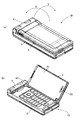
図1(a)および(b)は、本発明の実施の形態1の携帯端末装置としての携帯電話機10の全体概要図を示すものである。
本発明の実施の形態1の携帯電話機10は、図1に示すように、上部筐体2と下部筐体3とで構成され、上部筐体2と下部筐体3とがヒンジ4で結合されている。上部筐体2は、ヒンジ4又はヒンジ軸41を用いて、下部筐体3に対して図のX方向(縦方向)又はY方向(横方向)に回動することができる。上部筐体2には、筐体を折り畳んだ状態で下部筐体3と対向する面(図1(a)では下面)に液晶表示部21及び受話部22を設けている。下部筐体3には、筐体を折り畳んだ状態で上部筐体2と対向する面(図1では上面、表側の面)にキーボタン及び送話部を設けている。
(Embodiment 1)
Hereinafter, Embodiment 1 of the present invention will be described in detail with reference to the drawings.
1 (a) and 1 (b) show an overall schematic diagram of a
As shown in FIG. 1, the
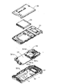
図2は、携帯電話機10の下部筐体3の分解斜視図(表側)である。図3は、図2とは逆側(裏側)から見た携帯電話機10下部筐体3の分解斜視図である。図2、3に示すように、携帯電話機10の下部筐体3は、ケース37とカバー31とで構成される。下部筐体3には、キーシート32、金属プレート33、シールド蓋34、回路基板35などが収められている。下部筐体3は、ケース37とカバー31とで構成され、これらを収納することで、作業性良く組み立てることができる。また、本実施の形態の携帯電話機10では、回路基板35の他にさらにサブ回路基板36も設けている。また、裏面側には、電池パック39、電池蓋38などを取り付けている。
FIG. 2 is an exploded perspective view (front side) of the
図4に、回路基板35、シールド蓋34、金属プレート33の拡大図を示す。図4に示すように、金属プレート33は、周縁に起立部331a、331bを有する。起立部331aには、切欠き332a、332b、332cが形成されている。この金属プレートは、厚さ0.3mm程度の金属板を打ち抜き加工し、折り曲げることで形成され、この金属プレート33で、下部筐体3の、高周波回路などを有する回路基板35をシールドする。
FIG. 4 shows an enlarged view of the
回路基板35には、金属プレート33の起立部331aの切欠き332a、332b、332cに対応した相対向する辺上に突起351a、351b、351cを有する。そして、回路基板35は、突起351a、351b、351cを切欠き332a、332b、332cに係止させることで金属プレート33に固定される。
The
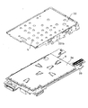
さらに、回路基板35の主面には、図2及び図5に示すように、シールド蓋34が取り付けられる。そして、シールド蓋34は、回路基板35と金属プレート33の間に介挿される。シールド蓋34は、前記シャーシ枠に弾性的に接触する切起し片を有する。回路基板35と金属プレート33の間に、このようなシールド蓋34を入れることで、キーボタンの押下、衝撃などを受けた場合でもシールド部材である金属プレート33と回路基板35の間のグランド接続を確実にすることで、確実なシールド効果を得て、衝撃に対する緩衝性を高めるようにしている。なお、このシールド蓋34は、厚さ0.1mm程度の金属板を打ち抜き加工し、折り曲げることで形成できる。
Further, a
図6は、回路基板35の主面にシールド蓋34を取り付けたものを金属プレート33に収めた様子を示す図である。図6に示すように、回路基板35は、突起351a、351b、351cを切欠き332a、332b、332cに係止させることで金属プレート33に固定されている。
FIG. 6 is a diagram illustrating a state in which a
図7は、図6に示した、回路基板35の主面にシールド蓋34を取り付けたものを金属プレート33に収めたものを、さらにキーシート32とともにカバー31に収めた様子を示す。図7に示すように、カバー31は、内側に凹部311a、311bを有する。また、回路基板35は、前述した突起351a、351b、351cに加えて、その反対の辺に他の突起351d、351eを有する。この回路基板35の他の突起351d、351eは、カバー31の凹部311a、311bに対応した相対向する辺上に位置する。そして、回路基板35は、他の突起351d、351eを凹部311a、311bに係止させることでカバーに固定される。
FIG. 7 shows a state in which the main surface of the
このような構成によれば、シールド部材として金属プレート33を用い、金属プレート33を薄くすることで、携帯端末装置10の薄型化を図ることができる。また、回路基板35を筐体の一部を構成するカバー31と金属プレート33とに係止させ、落下時などの衝撃を分散させることで、耐衝撃性の高い携帯電話機10を提供することができる。また、このような構成にすることにより、ネジなどを極力少なくすることができ、作業性良く安価に携帯電話機10を組み立てることができる。
According to such a configuration, it is possible to reduce the thickness of the mobile
次に、突起351a、351b、351c及び切欠き332a、332b、332c、並びに、他の突起351d、351e及び凹部311a、311bとサイドキー322a、322bとの関係について、図2、図6、図7を参照して、説明する。
図2に示すように、サイドキー322a、322bは、キーシート32の伸長部に設けられている。キーシート32には、フレキシブル基板上にドーム状のスイッチ部321が設けられている。そして、サイドキー322a、322bは、金属プレート33の起立部331bに取り付けられる(図2及び図7に示すサイドキー取り付け位置422a、422b参照)。そして、カバー31のサイドキー取り付け位置522a、522b(図2参照)に収められる。
Next, FIG. 2, FIG. 6, FIG. Will be described with reference to FIG.
As shown in FIG. 2, the
金属プレート33の起立部331bは、サイドキー322a、322bを取り付けるために、サイドキーを取り付けない起立部331aよりも高さを高くしている。また、サイドキー322a、322bを取り付ける起立部331bは、サイドキー322a、322bが押下されることがあるので、この分の強度が必要である。そのため、サイドキー322a、322bを取り付ける起立部331bは、強度確保の点から、起立部331aの切欠き332a、332b、332cと同様の形状の切欠きを設けることは望ましくない。また、仮に、この部分に切欠きを設けた場合には、サイドキー322a、322bが押下されたときに、回路基板35までその力が伝わりやすくなるので、回路基板35の強度確保の点からはあまり有効ではない。
In order to attach the
そこで、サイドキー322a、322bが取り付けられる部分(サイドキー取り付け位置422a、422b)に対応する回路基板35の部分には、突起351a、351b、351cや他の突起351d、351eは設けていない。そして、サイドキー322a、322bが取り付けられる部分でない部分のうち、サイドキー322a、322bが取り付けられる側に対応する回路基板35の辺には、図2及び図7に示すように、カバー31の凹部311a、311bに係止させるための、他の突起351d、351eを設けている。他方、サイドキーが取り付けられない側に対応する回路基板35の辺には、図2及び図6に示すように、金属プレート33の切欠き332a、332b、332cに係止させるための、突起351a、351b、351cを設けて、落下時などの衝撃を分散させている。
Therefore, the
このように、下部筐体3の側面に設けられたサイドキー322a、322bを備える携帯電話機10において、カバー31は、サイドキー322a、322bの設けられた側の側面の内側に凹部311a、311bを有し、金属プレート33は、サイドキー322a、322bの設けられた側面の反対側の起立部331aに切欠き332a、332b、332cが形成されている。
As described above, in the
この構成によれば、サイドキー322a、322bを取り付ける部分の金属プレート33の機械的強度を保ち、サイドキー322a、322bが押下されたときに、回路基板35までその力が伝わりにくくしつつ、下部筐体3全体として、薄型化を図りつつも落下時などの衝撃に対する耐性の高い携帯電話機10を提供することができる。
According to this configuration, the mechanical strength of the
なお、他の突起351eは、カバー31の凹部311bに係止させると同時に、金属プレート33の起立部331bの端部361にも係止させるようになっている。これは、サイドキー322bから比較的離れているからである。他方、サイドキー322aから比較的近い他の突起351dは、金属プレート33の起立部331bには係止させるようにはなっていない。
The
なお、上述の構成において、回路基板35の突起351a、351b、351c及び金属プレート33の切欠き332a、332b、332cの代わりに、逆に、金属プレートに突起を設け、この突起に対し回路基板の端面に設けた凹部を係合させる構造にしてもよい。
In the above-described configuration, instead of the
また、上述の構成において、回路基板35の他の突起351d、351e及びカバー31の凹部311a、311bの代わりに、逆に、カバーに突起を設け、この突起に対し回路基板の端面に設けた凹部を係合させる構造にしてもよい。
In the above-described configuration, instead of the
次に、図2、図4、図5などを用いて、回路基板35、金属プレート33、シールド蓋34などについてさらに詳しく説明する。
回路基板35の主面には、携帯電話機10の送受信部などを含む高周波回路や、種々の信号処理を行うアナログ回路、ディジタル回路などが形成されている。この回路基板35の主面には、シャーシ枠352、353が取り付けられている。シャーシ枠352、353は、シャーシ外枠352と、シャーシ内枠353との部分に分けて考えることができる。シャーシ枠352、353は回路基板35の外縁近傍に配設された外枠部(シャーシ外枠352)と、外枠部(シャーシ外枠352)に接触するとともに外枠部(シャーシ外枠352)で囲まれた領域を複数に分割する内枠部(シャーシ内枠353)とで構成される。シャーシ外枠352は、回路基板35上に、回路基板35上の回路を囲むように起立せしめられている。
Next, the
On the main surface of the
この構成によれば、回路基板35上の回路を囲むように起立せしめられたシャーシ枠(シャーシ外枠352)が、回路基板35上の回路を囲むため、より確実に回路に対するシールド性能を発揮できるようにすることが可能となる。また、複数に領域分割がなされているため回路基板35上の回路同士のシールド性を高めることができる。また、より近い位置でシールドできるため、シールド性能自体も良好である。なお、ここでシャーシ枠351、352の形状はこの構造に限定されるものではなく、必要に応じて適宜変更可能である。
According to this configuration, the chassis frame (chassis outer frame 352) erected so as to surround the circuit on the
シールド蓋34には、シャーシ枠352、353に弾性的に接触する切起し片341、342を有する。この切起し片341、342は、シャーシ枠の内枠部(シャーシ内枠353)に対向する位置に配設され、内枠部に弾性的に接触される。このうち、シールド蓋34の周縁部では、切起し片341は、中心に向かうV字状の形状に切り起こして形成される。他方、シールド蓋34の中心部では、切起し片は342、外方に向かうV字状の形状に切り起こして形成される。また、切起し片341、342は、それぞれ先端近傍に小突起Tを有する。
The
この構成によれば、シャーシ枠352、353に弾性的に接触する切起し片341、342を有するシールド蓋34を用いることで、キーボタン(スイッチ部321)の押下、衝撃などを受けた場合でも金属プレート33と回路基板35の間のグランド接続を確実にすることができるので、確実なシールド効果を得ることができ、衝撃に対する緩衝性を高めることができる。また、シャーシ枠(シャーシ内枠353)に対応して設けられ、弾性的に接触する切起し片341、342を用いているため、金属プレート33に多少の反りや歪が存在しても、切起し片341、342によりシャーシ枠(シャーシ内枠353)に確実に接触し、シールド性能を発揮し、衝撃に対する緩衝性を高めることができる。また、シールド蓋34の周縁部では、中心に向かうV字状の形状に切り起こしているため(切起し片341)、シールド蓋に反りや歪があったとしてもシャーシ枠(シャーシ内枠353)の周縁部と切起し片341とのより安定で、確実な電気的接触を得ることができる。また、シールド蓋34の中心部では、外方に向かうV字状の形状に切り起こしているため(切起し片342)、シールド蓋34に反りや歪があったとしてもシャーシ枠(シャーシ内枠353)の中心部と切起し片342とのより安定で、確実な電気的接触を得ることができる。また、切起し片341、342は、それぞれ先端近傍に小突起Tを有するので、点接触により確実な接触状態を得ることができる。なおこの小突起Tは、パンチングにより形成すれば極めて容易にかつ材料の付加もなく形成することができる。
According to this configuration, when the
金属プレート33には、回路基板35上に搭載される高周波回路に対向する位置を避けて孔hを形成している。この構成によれば、金属プレート33に孔hが設けられているため、軽量化を図ることができる。また、前記金属プレート33は、回路基板35上に搭載される高周波回路に対向する位置を避けて孔hを形成している。この構成によれば、高周波回路に対向する位置を避けて金属プレート33に孔hが設けられているため、高周波などによるノイズなどを低減し、シールド性能を発揮しつつ、軽量化を図ることができる。なお、この孔hは設けなくてもよく、重量と強度にあわせて、孔hの密度も適宜調整してもよい。
A hole h is formed in the
以上説明したように、本実施の形態の携帯電話機10によれば、シールド部材として金属プレート33を用い、金属プレート33を薄くすることで、携帯電話機10の薄型化を図ることができる。また、回路基板35を、筐体(下部筐体3)の一部を構成するカバー31と、金属プレート33とに係止させ、落下時などの衝撃を分散させることで、耐衝撃性の高い携帯電話機10を提供することができる。また、このような構成にすることにより、作業性良く安価に携帯電話機10を組み立てることもできる。
As described above, according to the
また、本実施の形態の携帯電話機10によれば、サイドキー322a、322bを取り付ける部分の機械的強度を保ち、サイドキーが押下されたときに、回路基板35までその力が伝わりにくくしつつ、筐体(下部筐体3)全体として、薄型化を図りつつも落下時などの衝撃に対する耐性の高い携帯電話機10を提供することができる。
Further, according to the
さらに、本実施の形態の携帯電話機10によれば、シャーシ枠(シャーシ内枠353)に弾性的に接触する切起し片341、342を有するシールド蓋34を用いることで、キーボタン(スイッチ部321)の押下、衝撃などを受けた場合でも金属プレート33と回路基板35の間のグランド接続を確実にすることができるので、確実なシールド効果を得ることができ、衝撃に対する緩衝性を高めることができる。
Furthermore, according to the
本発明の携帯端末装置は、シールド部材として金属プレートを用い、金属プレートを薄くすることで、携帯端末装置の薄型化を図ることができる。また、回路基板を筐体の一部を構成するカバーと金属プレートとに係止させ、落下時などの衝撃を分散させることで、耐衝撃性の高い携帯端末装置を提供することができる。また、このような構成にすることにより、作業性良く安価に携帯端末装置を組み立てることができる。これらのことから、本発明は、携帯電話機、PHS、PDA等を含む携帯端末装置への適用が可能である。 In the mobile terminal device of the present invention, a metal plate is used as the shield member, and the thickness of the mobile terminal device can be reduced by thinning the metal plate. In addition, it is possible to provide a mobile terminal device with high impact resistance by engaging the circuit board with a cover and a metal plate that constitute a part of the housing and dispersing the impact when dropped. Further, with such a configuration, the mobile terminal device can be assembled with good workability and at low cost. For these reasons, the present invention can be applied to mobile terminal devices including mobile phones, PHS, PDAs and the like.
10 携帯電話機(携帯端末装置)
2 上部筐体
3 下部筐体
4 ヒンジ部
41 ヒンジ軸
30 下部筐体
31 カバー
32 キーシート
33 金属プレート
34 シールド蓋
35 回路基板
36 サブ回路基板
37 ケース
38 電池蓋
39 電池パック
311a、311b 凹部
331a、331b 起立部
332a、332b、332c 切欠き
351a、351b、351c 突起
351d、351e 他の突起
361 端部
352 シャーシ外枠
353 シャーシ内枠
341、342 切起し片
10 Mobile phone (mobile terminal device)
2
Claims (2)
前記筐体の一部を構成し、内側に第1の凹部と第2の凹部とを有するカバーと、
前記筐体内に収納されるとともに、周縁に切欠きの形成された第1の起立部と、前記第1の起立部とは反対側の辺に形成された第2の起立部とを有する金属プレートと、
前記切欠きに対応した相対向する辺上に第1の突起を有し、前記第1の凹部に対応した相対向する辺上に第2の突起を有し、かつ、前記第2の突起を有する辺上であって前記第2の凹部に対応するとともに前記第2の起立部の端部に対応する位置に第3の突起を有する回路基板と、
を備え、
前記回路基板は、前記第1の突起を前記切欠きに係止させることで前記金属プレートに固定され、前記第2の突起を前記第1の凹部に係止させることで前記カバーに固定され、かつ、前記第3の突起を前記第2の起立部の端部に係止させることで前記金属プレートに固定されるとともに前記第2の凹部に係止させることで前記カバーに固定された携帯端末装置。 A case constituting a part of the housing;
A cover that constitutes a part of the housing and has a first recess and a second recess on the inside;
A metal plate that is housed in the housing and has a first upright portion having a notch formed in the periphery and a second upright portion formed on a side opposite to the first upright portion. When,
The has a first projection on the side which faces corresponding to the notch, before SL have a second projection on the side which faces corresponding to the first recess, and said second protrusion A circuit board having a third protrusion at a position corresponding to the second recessed portion and corresponding to the end of the second upright portion ,
With
The circuit board is fixed to said first projection on said metal plate by engaged in the notch, fixed front Stories second projections on the cover by engaged in the first recess In addition, the mobile phone fixed to the cover by being locked to the metal plate and locked to the second recess by locking the third protrusion to the end of the second upright portion. Terminal device.
前記筐体の側面に設けられたサイドキーを備え、
前記カバーは、前記サイドキーの設けられた側の側面の内側に前記第1の凹部を有し、
前記金属プレートは、前記サイドキーの設けられた側面の反対側の前記第1の起立部に前記切欠きの形成された携帯端末装置。 The mobile terminal according to claim 1,
A side key provided on a side surface of the housing;
The cover has the first recess on the inner side of the side key provided side;
The said metal plate is a portable terminal device by which the said notch was formed in the said 1st standing part on the opposite side to the side surface in which the said side key was provided.
Priority Applications (1)
| Application Number | Priority Date | Filing Date | Title |
|---|---|---|---|
| JP2007272192A JP4536103B2 (en) | 2007-10-19 | 2007-10-19 | Mobile terminal device |
Applications Claiming Priority (1)
| Application Number | Priority Date | Filing Date | Title |
|---|---|---|---|
| JP2007272192A JP4536103B2 (en) | 2007-10-19 | 2007-10-19 | Mobile terminal device |
Related Child Applications (1)
| Application Number | Title | Priority Date | Filing Date |
|---|---|---|---|
| JP2009254161A Division JP4889781B2 (en) | 2009-11-05 | 2009-11-05 | Mobile terminal device |
Publications (3)
| Publication Number | Publication Date |
|---|---|
| JP2009100402A JP2009100402A (en) | 2009-05-07 |
| JP2009100402A5 JP2009100402A5 (en) | 2010-01-07 |
| JP4536103B2 true JP4536103B2 (en) | 2010-09-01 |
Family
ID=40702953
Family Applications (1)
| Application Number | Title | Priority Date | Filing Date |
|---|---|---|---|
| JP2007272192A Expired - Fee Related JP4536103B2 (en) | 2007-10-19 | 2007-10-19 | Mobile terminal device |
Country Status (1)
| Country | Link |
|---|---|
| JP (1) | JP4536103B2 (en) |
Families Citing this family (1)
| Publication number | Priority date | Publication date | Assignee | Title |
|---|---|---|---|---|
| JP5789560B2 (en) | 2012-04-13 | 2015-10-07 | 京セラ株式会社 | Electronics |
Citations (9)
| Publication number | Priority date | Publication date | Assignee | Title |
|---|---|---|---|---|
| JPS54175211U (en) * | 1978-05-31 | 1979-12-11 | ||
| JPH10224074A (en) * | 1997-02-03 | 1998-08-21 | Matsushita Electric Ind Co Ltd | Method and apparatus for shielding electronic apparatus |
| JP2003283176A (en) * | 2002-03-25 | 2003-10-03 | Matsushita Electric Ind Co Ltd | Portable terminal device |
| JP2003348201A (en) * | 2002-05-29 | 2003-12-05 | Hitachi Ltd | Electronic apparatus |
| WO2004062336A1 (en) * | 2002-12-27 | 2004-07-22 | Sony Computer Entertainment Inc. | Electromagnetic shield plate, electromagnetic shield structure, and electronic device |
| JP2006270035A (en) * | 2005-02-25 | 2006-10-05 | Kyocera Corp | Mobile electronic apparatus |
| JP2007199930A (en) * | 2006-01-25 | 2007-08-09 | Nec Access Technica Ltd | Portable terminal equipment |
| JP2007208339A (en) * | 2006-01-30 | 2007-08-16 | Kyocera Corp | Portable electronic apparatus |
| JP2007227954A (en) * | 2007-04-05 | 2007-09-06 | Sony Corp | Case body, and receiver equipped with it |
-
2007
- 2007-10-19 JP JP2007272192A patent/JP4536103B2/en not_active Expired - Fee Related
Patent Citations (9)
| Publication number | Priority date | Publication date | Assignee | Title |
|---|---|---|---|---|
| JPS54175211U (en) * | 1978-05-31 | 1979-12-11 | ||
| JPH10224074A (en) * | 1997-02-03 | 1998-08-21 | Matsushita Electric Ind Co Ltd | Method and apparatus for shielding electronic apparatus |
| JP2003283176A (en) * | 2002-03-25 | 2003-10-03 | Matsushita Electric Ind Co Ltd | Portable terminal device |
| JP2003348201A (en) * | 2002-05-29 | 2003-12-05 | Hitachi Ltd | Electronic apparatus |
| WO2004062336A1 (en) * | 2002-12-27 | 2004-07-22 | Sony Computer Entertainment Inc. | Electromagnetic shield plate, electromagnetic shield structure, and electronic device |
| JP2006270035A (en) * | 2005-02-25 | 2006-10-05 | Kyocera Corp | Mobile electronic apparatus |
| JP2007199930A (en) * | 2006-01-25 | 2007-08-09 | Nec Access Technica Ltd | Portable terminal equipment |
| JP2007208339A (en) * | 2006-01-30 | 2007-08-16 | Kyocera Corp | Portable electronic apparatus |
| JP2007227954A (en) * | 2007-04-05 | 2007-09-06 | Sony Corp | Case body, and receiver equipped with it |
Also Published As
| Publication number | Publication date |
|---|---|
| JP2009100402A (en) | 2009-05-07 |
Similar Documents
| Publication | Publication Date | Title |
|---|---|---|
| US7957123B2 (en) | Portable electronic device | |
| US7561684B2 (en) | Mounting structure for an electroacoustic transducer | |
| EP3483982B1 (en) | Middle frame assembly and electronic device | |
| US8284569B2 (en) | Shield casing and electronic apparatus | |
| JP4833130B2 (en) | Electronics | |
| AU2006202755A1 (en) | Microphone coupler for communication device | |
| EP1100145A2 (en) | Portable radio communication device, such as a portable telephone | |
| JP5111937B2 (en) | Portable electronic devices | |
| JP4889781B2 (en) | Mobile terminal device | |
| JPWO2007037405A1 (en) | Mobile terminal device | |
| US7505072B2 (en) | Noise-reduced mobile communication apparatus | |
| US7391623B2 (en) | Display module and portable terminal apparatus | |
| JP4536103B2 (en) | Mobile terminal device | |
| US8138979B2 (en) | Portable wireless apparatus | |
| JP2003283176A (en) | Portable terminal device | |
| JP2010130101A (en) | Radio communication device | |
| JP4675775B2 (en) | Portable radio | |
| GB2379333A (en) | Electronic device casing | |
| JP4947582B2 (en) | Electronics | |
| JP4436292B2 (en) | Electronics | |
| JP5477882B2 (en) | Portable electronic devices | |
| JP2007199930A (en) | Portable terminal equipment | |
| JP5122306B2 (en) | Portable electronic devices | |
| KR100810295B1 (en) | Liquid crystal display module for mobile phone | |
| JP2009111696A (en) | Portable terminal, and microphone attaching method |
Legal Events
| Date | Code | Title | Description |
|---|---|---|---|
| A521 | Written amendment |
Free format text: JAPANESE INTERMEDIATE CODE: A523 Effective date: 20091113 |
|
| A621 | Written request for application examination |
Free format text: JAPANESE INTERMEDIATE CODE: A621 Effective date: 20091113 |
|
| A871 | Explanation of circumstances concerning accelerated examination |
Free format text: JAPANESE INTERMEDIATE CODE: A871 Effective date: 20091113 |
|
| A131 | Notification of reasons for refusal |
Free format text: JAPANESE INTERMEDIATE CODE: A131 Effective date: 20100316 |
|
| A521 | Written amendment |
Free format text: JAPANESE INTERMEDIATE CODE: A523 Effective date: 20100420 |
|
| A975 | Report on accelerated examination |
Free format text: JAPANESE INTERMEDIATE CODE: A971005 Effective date: 20100507 |
|
| TRDD | Decision of grant or rejection written | ||
| A01 | Written decision to grant a patent or to grant a registration (utility model) |
Free format text: JAPANESE INTERMEDIATE CODE: A01 Effective date: 20100518 |
|
| A01 | Written decision to grant a patent or to grant a registration (utility model) |
Free format text: JAPANESE INTERMEDIATE CODE: A01 |
|
| A61 | First payment of annual fees (during grant procedure) |
Free format text: JAPANESE INTERMEDIATE CODE: A61 Effective date: 20100615 |
|
| FPAY | Renewal fee payment (event date is renewal date of database) |
Free format text: PAYMENT UNTIL: 20130625 Year of fee payment: 3 |
|
| R150 | Certificate of patent or registration of utility model |
Free format text: JAPANESE INTERMEDIATE CODE: R150 |
|
| LAPS | Cancellation because of no payment of annual fees |