JP4533377B2 - Uneven light valve - Google Patents
Uneven light valve Download PDFInfo
- Publication number
- JP4533377B2 JP4533377B2 JP2006521358A JP2006521358A JP4533377B2 JP 4533377 B2 JP4533377 B2 JP 4533377B2 JP 2006521358 A JP2006521358 A JP 2006521358A JP 2006521358 A JP2006521358 A JP 2006521358A JP 4533377 B2 JP4533377 B2 JP 4533377B2
- Authority
- JP
- Japan
- Prior art keywords
- light valve
- imaging
- channel
- elements
- ribbon
- Prior art date
- Legal status (The legal status is an assumption and is not a legal conclusion. Google has not performed a legal analysis and makes no representation as to the accuracy of the status listed.)
- Expired - Fee Related
Links
Images


Classifications
-
- H—ELECTRICITY
- H04—ELECTRIC COMMUNICATION TECHNIQUE
- H04N—PICTORIAL COMMUNICATION, e.g. TELEVISION
- H04N1/00—Scanning, transmission or reproduction of documents or the like, e.g. facsimile transmission; Details thereof
- H04N1/024—Details of scanning heads ; Means for illuminating the original
- H04N1/028—Details of scanning heads ; Means for illuminating the original for picture information pick-up
- H04N1/03—Details of scanning heads ; Means for illuminating the original for picture information pick-up with photodetectors arranged in a substantially linear array
- H04N1/031—Details of scanning heads ; Means for illuminating the original for picture information pick-up with photodetectors arranged in a substantially linear array the photodetectors having a one-to-one and optically positive correspondence with the scanned picture elements, e.g. linear contact sensors
- H04N1/0311—Details of scanning heads ; Means for illuminating the original for picture information pick-up with photodetectors arranged in a substantially linear array the photodetectors having a one-to-one and optically positive correspondence with the scanned picture elements, e.g. linear contact sensors using an array of elements to project the scanned image elements onto the photodetectors
-
- B—PERFORMING OPERATIONS; TRANSPORTING
- B41—PRINTING; LINING MACHINES; TYPEWRITERS; STAMPS
- B41J—TYPEWRITERS; SELECTIVE PRINTING MECHANISMS, i.e. MECHANISMS PRINTING OTHERWISE THAN FROM A FORME; CORRECTION OF TYPOGRAPHICAL ERRORS
- B41J2/00—Typewriters or selective printing mechanisms characterised by the printing or marking process for which they are designed
- B41J2/435—Typewriters or selective printing mechanisms characterised by the printing or marking process for which they are designed characterised by selective application of radiation to a printing material or impression-transfer material
- B41J2/465—Typewriters or selective printing mechanisms characterised by the printing or marking process for which they are designed characterised by selective application of radiation to a printing material or impression-transfer material using masks, e.g. light-switching masks
-
- G—PHYSICS
- G02—OPTICS
- G02B—OPTICAL ELEMENTS, SYSTEMS OR APPARATUS
- G02B26/00—Optical devices or arrangements for the control of light using movable or deformable optical elements
- G02B26/02—Optical devices or arrangements for the control of light using movable or deformable optical elements for controlling the intensity of light
-
- G—PHYSICS
- G02—OPTICS
- G02B—OPTICAL ELEMENTS, SYSTEMS OR APPARATUS
- G02B26/00—Optical devices or arrangements for the control of light using movable or deformable optical elements
- G02B26/08—Optical devices or arrangements for the control of light using movable or deformable optical elements for controlling the direction of light
- G02B26/0816—Optical devices or arrangements for the control of light using movable or deformable optical elements for controlling the direction of light by means of one or more reflecting elements
- G02B26/0825—Optical devices or arrangements for the control of light using movable or deformable optical elements for controlling the direction of light by means of one or more reflecting elements the reflecting element being a flexible sheet or membrane, e.g. for varying the focus
-
- G—PHYSICS
- G02—OPTICS
- G02B—OPTICAL ELEMENTS, SYSTEMS OR APPARATUS
- G02B26/00—Optical devices or arrangements for the control of light using movable or deformable optical elements
- G02B26/08—Optical devices or arrangements for the control of light using movable or deformable optical elements for controlling the direction of light
- G02B26/0816—Optical devices or arrangements for the control of light using movable or deformable optical elements for controlling the direction of light by means of one or more reflecting elements
- G02B26/0833—Optical devices or arrangements for the control of light using movable or deformable optical elements for controlling the direction of light by means of one or more reflecting elements the reflecting element being a micromechanical device, e.g. a MEMS mirror, DMD
- G02B26/0841—Optical devices or arrangements for the control of light using movable or deformable optical elements for controlling the direction of light by means of one or more reflecting elements the reflecting element being a micromechanical device, e.g. a MEMS mirror, DMD the reflecting element being moved or deformed by electrostatic means
-
- G—PHYSICS
- G02—OPTICS
- G02F—OPTICAL DEVICES OR ARRANGEMENTS FOR THE CONTROL OF LIGHT BY MODIFICATION OF THE OPTICAL PROPERTIES OF THE MEDIA OF THE ELEMENTS INVOLVED THEREIN; NON-LINEAR OPTICS; FREQUENCY-CHANGING OF LIGHT; OPTICAL LOGIC ELEMENTS; OPTICAL ANALOGUE/DIGITAL CONVERTERS
- G02F1/00—Devices or arrangements for the control of the intensity, colour, phase, polarisation or direction of light arriving from an independent light source, e.g. switching, gating or modulating; Non-linear optics
- G02F1/01—Devices or arrangements for the control of the intensity, colour, phase, polarisation or direction of light arriving from an independent light source, e.g. switching, gating or modulating; Non-linear optics for the control of the intensity, phase, polarisation or colour
- G02F1/13—Devices or arrangements for the control of the intensity, colour, phase, polarisation or direction of light arriving from an independent light source, e.g. switching, gating or modulating; Non-linear optics for the control of the intensity, phase, polarisation or colour based on liquid crystals, e.g. single liquid crystal display cells
- G02F1/133—Constructional arrangements; Operation of liquid crystal cells; Circuit arrangements
- G02F1/1333—Constructional arrangements; Manufacturing methods
- G02F1/1343—Electrodes
- G02F1/134309—Electrodes characterised by their geometrical arrangement
-
- H—ELECTRICITY
- H04—ELECTRIC COMMUNICATION TECHNIQUE
- H04N—PICTORIAL COMMUNICATION, e.g. TELEVISION
- H04N1/00—Scanning, transmission or reproduction of documents or the like, e.g. facsimile transmission; Details thereof
- H04N1/024—Details of scanning heads ; Means for illuminating the original
- H04N1/028—Details of scanning heads ; Means for illuminating the original for picture information pick-up
- H04N1/03—Details of scanning heads ; Means for illuminating the original for picture information pick-up with photodetectors arranged in a substantially linear array
- H04N1/031—Details of scanning heads ; Means for illuminating the original for picture information pick-up with photodetectors arranged in a substantially linear array the photodetectors having a one-to-one and optically positive correspondence with the scanned picture elements, e.g. linear contact sensors
- H04N1/0314—Details of scanning heads ; Means for illuminating the original for picture information pick-up with photodetectors arranged in a substantially linear array the photodetectors having a one-to-one and optically positive correspondence with the scanned picture elements, e.g. linear contact sensors using photodetectors and illumination means mounted in the same plane on a common support or substrate
-
- G—PHYSICS
- G02—OPTICS
- G02F—OPTICAL DEVICES OR ARRANGEMENTS FOR THE CONTROL OF LIGHT BY MODIFICATION OF THE OPTICAL PROPERTIES OF THE MEDIA OF THE ELEMENTS INVOLVED THEREIN; NON-LINEAR OPTICS; FREQUENCY-CHANGING OF LIGHT; OPTICAL LOGIC ELEMENTS; OPTICAL ANALOGUE/DIGITAL CONVERTERS
- G02F1/00—Devices or arrangements for the control of the intensity, colour, phase, polarisation or direction of light arriving from an independent light source, e.g. switching, gating or modulating; Non-linear optics
- G02F1/01—Devices or arrangements for the control of the intensity, colour, phase, polarisation or direction of light arriving from an independent light source, e.g. switching, gating or modulating; Non-linear optics for the control of the intensity, phase, polarisation or colour
- G02F1/13—Devices or arrangements for the control of the intensity, colour, phase, polarisation or direction of light arriving from an independent light source, e.g. switching, gating or modulating; Non-linear optics for the control of the intensity, phase, polarisation or colour based on liquid crystals, e.g. single liquid crystal display cells
- G02F1/133—Constructional arrangements; Operation of liquid crystal cells; Circuit arrangements
- G02F1/1333—Constructional arrangements; Manufacturing methods
- G02F1/1335—Structural association of cells with optical devices, e.g. polarisers or reflectors
- G02F1/133509—Filters, e.g. light shielding masks
- G02F1/133514—Colour filters
- G02F1/133516—Methods for their manufacture, e.g. printing, electro-deposition or photolithography
Abstract
Description
本発明はイメージングシステムに関する。本発明の特定実施形態は、イメージングシステムで使用するための光弁(ライトバルブ)を提供する。 The present invention relates to an imaging system. Certain embodiments of the present invention provide a light valve for use in an imaging system.
ディスプレイ装置、ポリマーベースの半導体装置及び他の半導体装置の製造方法には、通常、比較的多数のイメージング工程が含まれる。従来のフォトリソグラフィーによるイメージング処理においては、各イメージング工程が以下の工程を含む。すなわち、基板にレジスト(または他の感光材料)を被覆する工程と、被覆した基板をフォトツールマスクを介して露光し、対応する変化をレジストに起こす工程と、露光された材料を現像処理する工程と、を含む。 Display devices, polymer-based semiconductor devices, and other semiconductor device fabrication methods typically include a relatively large number of imaging steps. In a conventional photolithography imaging process, each imaging step includes the following steps. That is, a step of coating a substrate with a resist (or other photosensitive material), a step of exposing the coated substrate through a phototool mask to cause a corresponding change in the resist, and a step of developing the exposed material And including.
一般に、各イメージング工程に関連して失敗の恐れが有限にある。多数のイメージング工程を含む製造方法の場合、このような失敗の恐れは倍加し、その結果、全体的な処理歩留まりが減少するとともに完成品のコストが上がる。フラットパネルディスプレイ(例えば、液晶ディスプレイ(LCD))のカラーフィルタ製造は、複数工程による製造方法の特定例である。カラーフィルタの製造は、材料コストが高く、処理歩留まりが低いために、極めて高価な製法となり得る。 In general, there is a finite risk of failure associated with each imaging step. For manufacturing methods involving multiple imaging steps, the risk of such failure is doubled, resulting in a reduction in overall processing yield and an increase in the cost of the finished product. The manufacture of color filters for flat panel displays (e.g., liquid crystal displays (LCDs)) is a specific example of a multi-step manufacturing method. The manufacture of color filters can be a very expensive manufacturing process due to high material costs and low processing yield.
ディスプレイの製造及び特定カラーフィルタに使用されるダイレクトイメージングが提案されている。デボア(DeBoer)他に付与された米国特許第4,965,242号には、カラーフィルタ要素を製造するためのダイレクトイメージング染料転写方法が記載されている。この方法では、染料受け取り要素を染料ドナー要素に重ねて置き、染料ドナー要素を画像に関して加熱することで染料を染料ドナー要素から染料受け取り要素に転写する。画像に関する加熱の好ましい方法は、レーザビームによる方法である。ダイオードレーザは、変調が容易で、コストが低く、かつ小型であるため、特に好ましい。 Direct imaging used for display manufacture and specific color filters has been proposed. U.S. Pat. No. 4,965,242 to DeBoer et al. Describes a direct imaging dye transfer method for producing color filter elements. In this method, the dye receiving element is placed over the dye donor element and the dye donor element is heated with respect to the image to transfer the dye from the dye donor element to the dye receiving element. A preferred method of heating for the image is by a laser beam. Diode lasers are particularly preferred because they are easy to modulate, low in cost, and small in size.
上記のデボア特許によるダイレクトイメージング技術の欠点は、画像に関連する染料の転写を実現するためには、基板表面全体にレーザビームをスキャンする必要があるという点である。このような画像に関するスキャンは、フォトツールマスクを使用するフラッド露光(flood exposure)に比べて、比較的長い時間を要する。これは、フラッド露光では、小型の基板は一度に露光され、より大型の基板の場合、一連の高速ステップ繰り返し露光による露光が可能であるためである。 The disadvantage of the direct imaging technique according to the above-mentioned Deborah patent is that a laser beam needs to be scanned over the entire substrate surface in order to achieve transfer of the dye associated with the image. Such a scan for an image takes a relatively long time compared to a flood exposure using a phototool mask. This is because in the flood exposure, a small substrate is exposed at one time, and in the case of a larger substrate, exposure can be performed by a series of high-speed stepwise repeated exposures.
ダイレクトイメージングの速度を上げる1つの方法として、独立的に変調可能な複数のレーザビームによって基板を同時にスキャンすることが考えられる。ブランシェ−フィンチャ(Blanchet−Fincher)他による米国特許第6,146,792号には、受け取り要素、例えばカラーフィルタへの恒久的画像の生成が記載される。ブランシェ−フィンチャ特許が示唆するレーザヘッドは、32個の820nmレーザダイオードを含み、各レーザダイオードが約90mWの単一モード出力を有する。 One method for increasing the speed of direct imaging is to simultaneously scan the substrate with a plurality of laser beams that can be modulated independently. U.S. Pat. No. 6,146,792 by Blanchet-Fincher et al. Describes the generation of a permanent image on a receiving element, e.g. a color filter. The laser head suggested by the Blanche-Fincher patent includes 32 820 nm laser diodes, each laser diode having a single mode output of approximately 90 mW.
独立的に変調可能なレーザビームは、当業界ではしばしば「チャネル」と呼ばれる。現在、さらに多数のチャネルを備えたイメージングヘッドが入手可能である。このようなイメージングヘッドの一例が、クレオ社(カナダ、ブリティッシュコロンビア州バーナビー)により製造されたスクエアスポット(SQUAREspot:登録商標)サーマルイメージングヘッドである。このイメージングヘッドは、最大240個の独立的に変調可能なチャネルを備えることができ、各チャネルは約100mWの光出力を有する。450mJ/cm2の媒体感光度に対し、このイメージングヘッドは、370x470mmの小型カラーフィルタ基板を約3分間で描画(imaging)することができる。 An independently modulatable laser beam is often referred to in the art as a “channel”. Currently, imaging heads with more channels are available. One example of such an imaging head is a square spot (SQUAREspot®) thermal imaging head manufactured by Creo (Burnaby, British Columbia, Canada). The imaging head can comprise up to 240 independently modifiable channels, each channel having a light output of about 100 mW. For a medium sensitivity of 450 mJ / cm 2 , this imaging head can image a small color filter substrate of 370 × 470 mm in about 3 minutes.
イメージング速度のさらなる改善は、イメージング解像度と速度とのトレードオフにより妨げられてきた。望ましいエッジ鮮明度特性(すなわち、高解像度)を有するカラーフィルタの生成には、対応する小型画素サイズでのイメージングが要求される(すなわち、各チャネルに関連するビームが、対応する小サイズを有すべく集束されなければならない)。ところが、小型画素サイズのイメージングの場合、所望のイメージング領域全体の画像に関する露光を実現するのに時間がかかる。これは、所望のイメージング領域を完全にカバーするために、イメージングヘッドを基板全体にスキャンするのに時間がかかるためである。イメージングヘッドにさらに多数のチャネルを追加しても、そのようなイメージングヘッドを経済的かつ実際的なイメージングシステムで提供するのは困難であるため、上記の問題の完全な解決策にはならない。 Further improvements in imaging speed have been hampered by the trade-off between imaging resolution and speed. Generation of color filters with desirable edge sharpness characteristics (ie, high resolution) requires imaging with a corresponding small pixel size (ie, the beam associated with each channel has a corresponding small size) Must be focused as much as possible). However, in the case of imaging with a small pixel size, it takes time to realize exposure related to the image of the entire desired imaging region. This is because it takes time to scan the imaging head across the substrate in order to completely cover the desired imaging area. Adding more channels to the imaging head is not a complete solution to the above problem because it is difficult to provide such an imaging head in an economical and practical imaging system.
ディスプレイ製造業では、より大型の基板を処理する一般的な傾向がある。大型の基板の使用により大型のディスプレイを製造できる。さらに、大型の基板を処理し、その後これをより小型のパネルに分離することにより、小型ディスプレイの製造に関して経済性及び歩留まりを向上させることができる。例えば、4パネル基板に2つの欠陥品があれば歩留まりは50%になり得るが、同じ2つの欠陥が12パネル基板にある場合には、その歩留まりは83%である。 In the display manufacturing industry, there is a general tendency to process larger substrates. Large displays can be manufactured by using large substrates. Furthermore, by processing a large substrate and then separating it into smaller panels, the economy and yield can be improved with respect to the manufacture of small displays. For example, if there are two defective products on a 4-panel substrate, the yield can be 50%, but if the same two defects are on a 12-panel substrate, the yield is 83%.
ディスプレイ製造業においては、いわゆる「第6世代」フラットパネルディスプレイの基板サイズは約1500x1800mmである。媒体感光度が450mJ/cm2であるこのサイズの基板に対し、上記の240チャネルSQUAREspot(登録商標)サーマルイメージングヘッドが要するイメージング時間は約45分と、法外に長い。 In the display manufacturing industry, the substrate size of so-called “sixth generation” flat panel displays is about 1500 × 1800 mm. For a substrate of this size with a media sensitivity of 450 mJ / cm 2 , the imaging time required for the 240 channel SQUAREspot® thermal imaging head is approximately 45 minutes, which is prohibitively long.
したがって、種々の製造処理に使用できる、より生産性の高いダイレクトイメージング技術が求められている。
本発明の第1の態様は、イメージングシステムに使用される光弁を提供する。光弁は、独立して駆動可能な複数のチャネルを含む。これらのチャネルのうち少なくとも2つが、描画(イメージング)される規則的パターンに対応する不均一なサイズを有する。 A first aspect of the invention provides a light valve for use in an imaging system. The light valve includes a plurality of channels that can be independently driven. At least two of these channels have a non-uniform size corresponding to the regular pattern being imaged.
チャネルは、不均一数の個別光弁要素を含んでもよい。チャネルは、イメージングされるパターンの特徴(feature)に対応する1つ以上の低解像度チャネル、及び/またはイメージングされるパターンの特徴の端部(エッジ)に対応する1つ以上の高解像度チャネルを含んでもよい。低解像度チャネルは、ドライバに電気的に結合した複数の個別光弁要素を含んでもよい。1つ以上の高解像度チャネルを、低解像度チャネルの片側または両側に隣接配置してもよい。 The channel may include a non-uniform number of individual light valve elements. The channel includes one or more low resolution channels corresponding to the features of the pattern being imaged and / or one or more high resolution channels corresponding to the edges of the features of the pattern being imaged. But you can. The low resolution channel may include a plurality of individual light valve elements electrically coupled to the driver. One or more high resolution channels may be placed adjacent to one or both sides of the low resolution channel.
光弁は、均一(規則正しい)間隔で離間した複数の光弁要素を含んでもよく、光弁要素群が互いに電気的に結合することで、低解像度チャネル及び高解像度チャネルを形成する。電気的に結合されて低解像度チャネルを形成する光弁要素の数は、電気的に結合されて高解像度チャネルを形成する光弁要素の数より多くてもよい。均一間隔で離間した光弁要素の1つ以上が、低解像度チャネルと高解像度チャネルのいずれにも電気的に結合しなくてもよい。 The light valve may include a plurality of light valve elements spaced at uniform (regular) intervals, and the light valve element groups are electrically coupled together to form a low resolution channel and a high resolution channel. The number of light valve elements that are electrically coupled to form the low resolution channel may be greater than the number of light valve elements that are electrically coupled to form the high resolution channel. One or more of the uniformly spaced light valve elements may not be electrically coupled to either the low resolution channel or the high resolution channel.
チャネルは、低解像度ドライバによって駆動されるべく結合された低解像度の個別光弁要素を有する低解像度光弁要素群と、高解像度ドライバによって駆動されるべく結合された高解像度の個別光弁要素を有する高解像度光弁要素群とを含んでもよい。低解像度の数は高解像度の数より大きくてもよい。低解像度の数及び高解像度の数は、イメージングされるパターンに対応すべく選択してもよい。低解像度群は、イメージングされる基板上に、対応する低解像チャネルを生成してもよく、高解像度群は、イメージングされる基板上に、対応する高解像チャネルを生成してもよい。低解像度チャネルは、高解像度チャネルより多くてもよい。低解像度の数は、低解像度チャネルの大きさが、イメージングされるパターンの特徴の内部部分の大きさに対応するように選択してもよい。高解像度の数は、高解像度チャネルの大きさが、イメージングされるパターンにおけるエッジ解像度要件を満たすべく十分に小さくなるように選択してもよい。1つ以上の高解像度チャネルが、低解像度チャネルの片側または両側に隣接して配置されてもよい。 The channel comprises a group of low resolution light valve elements having low resolution individual light valve elements coupled to be driven by a low resolution driver and a high resolution individual light valve element coupled to be driven by a high resolution driver. And a high-resolution light valve element group. The number of low resolutions may be greater than the number of high resolutions. The low resolution number and the high resolution number may be selected to correspond to the pattern being imaged. The low resolution group may generate a corresponding low resolution channel on the substrate to be imaged, and the high resolution group may generate a corresponding high resolution channel on the substrate to be imaged. There may be more low resolution channels than high resolution channels. The number of low resolutions may be selected such that the size of the low resolution channel corresponds to the size of the internal portion of the feature of the pattern being imaged. The high resolution number may be selected such that the size of the high resolution channel is small enough to meet the edge resolution requirements in the pattern being imaged. One or more high resolution channels may be located adjacent to one or both sides of the low resolution channel.
光弁は、さらなる光弁要素群を備えてもよく、このさらなる光弁要素群は低解像度群及び高解像度群から離間して配置してもよい。その間隔は、イメージングされるパターンにおける特徴どうしの間隙に一致すべく選択してもよい。光弁は、カラーフィルタ基板上にカラー要素をイメージングするために使用されるイメージングヘッドの一部であってもよい。光弁は、窒化ケイ素リボンベースの光弁でも、PLZT光弁でも、TIR光弁でも、格子光弁でもよい。個別光弁要素は、電子的に可変の反射特性を有するミラー要素でも、電子的に可変の屈折特性を有するレンズ要素でも、電子的に可変の透過特性を有する格子要素でもよい。 The light valve may comprise an additional group of light valve elements, which further group of light valve elements may be spaced apart from the low resolution group and the high resolution group. The spacing may be selected to match the gap between features in the pattern being imaged. The light valve may be part of an imaging head that is used to image the color elements on the color filter substrate. The light valve may be a silicon nitride ribbon based light valve, a PLZT light valve, a TIR light valve, or a grating light valve. The individual light valve element may be a mirror element having an electronically variable reflection characteristic, a lens element having an electronically variable refraction characteristic, or a grating element having an electronically variable transmission characteristic.
本発明の別の態様は、特徴の規則的パターンを基板にイメージングするイメージング装置を提供する。イメージング装置は、イメージングされる規則的パターンに対応する不均一なサイズを有する独立的に駆動可能な複数のチャネルを有する光弁を含む。イメージング装置は、さらに、光弁を照射する光線源と、基板上に光弁をイメージングするレンズとを含む。 Another aspect of the invention provides an imaging apparatus for imaging a regular pattern of features on a substrate. The imaging device includes a light valve having a plurality of independently actuable channels having a non-uniform size corresponding to the regular pattern to be imaged. The imaging device further includes a light source that illuminates the light valve and a lens that images the light valve on the substrate.
本発明の別の態様は、マルチチャネルイメージングヘッドによって、特徴の規則的パターンを基板上にイメージングする方法を提供する。この方法では、パターンを分析して1つ以上の特徴の空間的特性を識別し、前記1つ以上の特徴のそれぞれの内部部分を対応する低解像度チャネルによってイメージングし、前記1つ以上の特徴のそれぞれのエッジ部分を、少なくとも1つの対応する高解像度チャネルによってイメージングする。少なくとも1つの対応する高解像度チャネルの大きさは、対応する低解像度チャネルより小さい。 Another aspect of the invention provides a method of imaging a regular pattern of features on a substrate with a multi-channel imaging head. In this method, a pattern is analyzed to identify spatial characteristics of one or more features, each internal portion of the one or more features is imaged by a corresponding low resolution channel, and the one or more features of the one or more features are imaged. Each edge portion is imaged by at least one corresponding high resolution channel. The size of the at least one corresponding high resolution channel is smaller than the corresponding low resolution channel.
本発明のさらに別の態様は、マルチチャネルイメージングシステムによって特徴のパターンをイメージングする光弁の製造方法を提供する。この方法では、特徴のパターンを分析してその1つ以上の空間的特性を識別し、規則的に離間配置された複数の均一な光弁要素を光弁基板上に製造し、前記特徴のパターンの空間的特性に基づき、少なくとも1つの低解像度光弁要素群を電気的に結合し、少なくとも1つの高解像度光弁要素群を電気的に結合する。 Yet another aspect of the present invention provides a method of manufacturing a light valve for imaging a pattern of features with a multi-channel imaging system. In this method, a pattern of features is analyzed to identify one or more spatial characteristics thereof, and a plurality of regularly spaced uniform light valve elements are fabricated on the light valve substrate, The at least one low resolution light valve element group is electrically coupled and the at least one high resolution light valve element group is electrically coupled.
本発明のさらに別の態様は、イメージングシステムに使用する光弁を提供する。光弁は、第1の数の互いに電気的に結合された個別光弁要素を有する第1光弁要素群と、第2の数の互いに電気的に結合された個別光弁要素を有する第2光弁要素群とを含む。光弁要素の第1の数と光弁要素の第2の数は互いに異なる。 Yet another aspect of the invention provides a light valve for use in an imaging system. The light valve includes a first light valve element group having a first number of individually light valve elements electrically coupled to each other and a second number having a second number of individually light valve elements electrically coupled to each other. Light valve element group. The first number of light valve elements and the second number of light valve elements are different from each other.
本発明の特定実施形態のさらなる特性及び応用が、以下に記載される。 Additional features and applications of specific embodiments of the invention are described below.
以下の説明を通じ、本発明のより徹底的な理解のために、特定の詳細について述べる。しかしながら、本発明はこれらの詳細なしに実施してもよい。他の例では、発明を不必要に不明瞭にしないために、周知の要素については詳細に示したり説明していない。したがって、明細書及び図面は、制限的ではなく、例示的な意味で理解すべきである。 Throughout the following description, specific details are set forth in order to provide a more thorough understanding of the present invention. However, the present invention may be practiced without these details. In other instances, well-known elements have not been shown or described in detail to avoid unnecessarily obscuring the invention. The specification and drawings are, accordingly, to be understood in an illustrative sense rather than a restrictive sense.
本発明は、イメージング装置に関する。発明の特定実施形態では、イメージング装置に使用される光弁を提供する。このような光弁は、個々に変調可能な複数のチャネルを生成することができる。このチャネルの2つ以上が異なる(不均一)の大きさを有する。チャネルの不均一な大きさは、イメージングされる規則的パターンに一致するよう選択される。本発明の特定実施形態による光弁は、低解像度ドライバによって独立的に駆動されるべく結合された低解像度の個別光弁要素(a low resolution number of individual light valve elements)を有する少なくとも1つの低解像度光弁要素群と、高解像度ドライバによって独立的に駆動されるべく結合された高解像度の個別光弁要素(a high resolution number of individual light valve elements)を有するの少なくとも1つの高解像度光弁要素群と、を含む。異なる(不均一な)大きさの低解像度チャネルと高解像度チャネルを生成するために、低解像度の数(the low resolution number)と高解像度の数(the high resolution number)とは互いに異なっている。本発明の他の実施形態は、かかる光弁を組み込んだイメージングヘッド及びイメージング装置、及びかかる光弁の製造及び使用方法を提供する。 The present invention relates to an imaging apparatus. In a particular embodiment of the invention, a light valve for use in an imaging device is provided. Such light valves can generate multiple channels that can be individually modulated. Two or more of the channels have different (non-uniform) sizes. The non-uniform size of the channel is selected to match the regular pattern being imaged. A light valve according to certain embodiments of the present invention includes at least one low resolution having a low resolution number of individual light valve elements coupled to be independently driven by a low resolution driver. At least one high resolution light valve element having a light valve element group and a high resolution number of individual light valve elements coupled to be independently driven by a high resolution driver And including. The low resolution number and the high resolution number are different from each other in order to generate different (non-uniform) sized low and high resolution channels. Other embodiments of the present invention provide imaging heads and imaging devices incorporating such light valves, and methods for making and using such light valves.
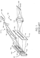
図1は、従来技術の光弁100を組み込んだイメージングヘッド115の光学システムを示す図である。光弁100は、シリコン基板102上に製造され、複数の変形可能なリボン要素101を含む。図示された実施形態においては、各リボン要素101が、穴(図示せず)を覆って懸架された窒化ケイ素リボンを含む。各リボン要素101には、さらに、反射性の金属材料、例えばアルミニウムが被覆され、これが反射表面及び電極として機能する。光弁100の後面は、共通電極(図示せず)を含み、この共通電極は通常接地に接続されている。
FIG. 1 is a diagram illustrating an optical system of an
ドライバ回路(図示せず)は、通常各リボン要素101に対応づけられ、これに選択的に電圧を印加する。図1の例では、リボン要素121は作動されたリボン要素の例を示している。ミラー121に対応するドライバは、リボン要素121の電極に電圧を印加することにより、リボン要素121及び光弁100の後面の共通電極に静電力を生成する。この静電力によりリボン要素121は穴の内部に向かって変形し、図示されるような湾曲した反射表面を生成する。リボン要素122は、非作動リボン要素の一例を示す。リボン要素122には電圧が印加されていないので、リボン要素123は穴に向かって変形することなく、図示されるような平坦な反射表面を維持する。
A driver circuit (not shown) is normally associated with each
イメージングヘッド115は、さらに、レーザ104とアナモルフィックビーム拡大器111とを含む。レーザ104からの光線105は、紫外線から赤外線までの広い波長範囲であってもよい。アナモルフィックビーム拡大器111は、1対のシリンドリカルレンズ108及び110を含む。ビーム拡大器111及びレーザ104は、レーザ104からの光線105がビーム拡大器111に向けられると、照射ライン106(図1では破線で示されている)が光弁100に生成されるように構成されている。図示される実施形態では、照射ライン106が光弁100のリボン要素101のすべてを横切って伸び、各リボン要素101が照射ライン106から光線の一部を受光している。光弁100に照射ライン106を生成する方法は、米国特許第5,517,359号(その記載内容が本願の一部としてここに援用されている)に記載されている。
The
イメージングヘッド115は、さらに、ストップ116とイメージングレンズ118とを含む。ストップ116は、透過領域114と非透過領域113とを有する。照射ライン106からの光線は、光弁100のリボン要素101から反射する。特定のリボン要素(例えば、リボン要素121)が電圧の印加によって変形している場合、その湾曲したミラー表面が反射した光線を集束し、その結果、反射した光線は透過領域114を通過してレンズ118の方向に進む。これに対し、特定のリボン要素(例えば、リボン要素122)が変形していない場合、その平坦なミラー表面によって反射された光線は拡散し、非透過領域113によってブロックされる。
The
イメージングレンズ118は光弁100をイメージングしてイメージング帯(imaging swath)120を形成する。イメージング帯120は、個々に変調された複数のビームまたはチャネル126を含む。イメージング帯120が基板(図示せず)上に集束されるように、基板をイメージングレンズ118に対して配置することができる。イメージング帯120が基板の所望するイメージング領域全体にスキャンされてこの領域に画像を形成することができる。特定のリボン要素101が作動されていれば、その表面から反射した光線が透過領域114を通過し、それに対応するチャネル126が十分な光線量を含み、基板を変更する。逆に、特定のリボン要素101が作動されていなければ、その表面から反射した光線の実質量が非透過領域113によって遮断され、対応するチャネルは基板を実質的に変える十分量の光線を含まない。
The
イメージングヘッド115及び光弁100の動作のさらなる詳細が、米国特許第6,147,789号(その記載内容を本願の一部としてここに援用する)に記載されている。
Further details of the operation of the
ここに記載される本発明の特定実施形態は、イメージングヘッド、例えばイメージングヘッド115に使用される光弁を提供する。本発明の光弁は、例えば、光弁100の代わりに使用できる。
Certain embodiments of the invention described herein provide a light valve for use with an imaging head, eg,
ディスプレイパネル用のカラーフィルタを製造する場合(または他の硬い基板をイメージングする場合)、イメージングヘッド、例えばイメージングヘッド115は、通常フラットベッドイメージング装置(「フラットベッドスキャナ」とも称される)において使用される。フラットベッドイメージング装置を使用する場合、通常、基板をフラットな方位に固定し、それから基板とイメージングヘッド、及び/または基板とイメージングヘッドとの組み合わせを互いに対して移動させて走査を行う。この走査には、通常、第1方向(「メイン走査方向」と呼ぶ)におけるイメージングヘッドと基板との相対移動を含む。走査には、さらに、イメージングヘッドの基板に対する(あるいはこの逆)第2方向(「サブ走査方向」と呼ぶ)のステッピング、及びその後に、イメージングヘッドの基板に対する(あるいはこの逆)再びメイン走査方向への移動を含んでもよい。この処理を、基板の所望イメージング領域が完全にイメージングされるまで繰り返してもよい。本発明との使用に適した高速フラットベッドスキャナが、米国特許公報第2004/004122号(その記載内容を本願の一部としてここに援用する)に開示されている。
When manufacturing color filters for display panels (or when imaging other rigid substrates), imaging heads, such as
ドラムベースのイメージング装置においては、可撓性の基板をドラムの内部または外部表面に固定してイメージングを行うことができる。通常、このようなドラムは円筒形である。走査は、ドラムをその軸を中心に回転させ、基板がイメージングヘッドに対してメイン走査方向に移動するようにする。走査には、さらに、イメージングヘッドをドラム及び基板に対して(あるいはこの逆)サブ走査方向にステッピングし、その後、ドラムを回転させて再びメイン走査方向における相対移動を生成してもよい。フラットベッドスキャナの場合と同様に、基板における所望のイメージング領域が完全にイメージングされるまでこの処理を繰り返すことができる。ドラムベースのイメージング装置を使用して、従来から剛性であると考えられている基板をイメージングすることができる。例えば、基板が十分に薄く、ドラムの直径が十分に大きければ、ガラス基板をドラムスキャナでイメージングすることができる。 In a drum-based imaging apparatus, imaging can be performed with a flexible substrate fixed to the interior or exterior surface of the drum. Usually, such a drum is cylindrical. Scanning rotates the drum about its axis so that the substrate moves in the main scanning direction relative to the imaging head. For scanning, the imaging head may be stepped with respect to the drum and the substrate (or vice versa) in the sub-scanning direction, and then the drum is rotated to generate relative movement in the main scanning direction again. As with the flatbed scanner, this process can be repeated until the desired imaging area on the substrate is fully imaged. A drum-based imaging device can be used to image a substrate that has traditionally been considered rigid. For example, if the substrate is thin enough and the drum diameter is large enough, the glass substrate can be imaged with a drum scanner.
すでに簡単に述べたように、光弁は通常そのリボン要素のそれぞれに対してドライバ回路を備える。多くの光弁では、このドライバの必要性が、光弁が収容できるリボン要素の数に関する限定要素となる。例えば、1つの光弁に関するドライバの数は通常、以下の要因により制限される。すなわち、多数のドライバを光弁に近接して設ける場合の空間的制限要素、ドライバ回路の切替により発生する熱の除去に関する熱除去制限要素、及び/またはドライバと対応するリボン要素との電気的接続に関する接続制限要素である。これらの制限により、さらに、光弁ベースのプリントヘッドにより同時にイメージングできるチャネルの数にも対応する制限が生じる。 As already mentioned briefly, a light valve usually comprises a driver circuit for each of its ribbon elements. In many light valves, the need for this driver becomes a limiting factor regarding the number of ribbon elements that the light valve can accommodate. For example, the number of drivers for one light valve is usually limited by the following factors: That is, a spatial restriction element when a large number of drivers are provided close to the light valve, a heat removal restriction element related to removal of heat generated by switching the driver circuit, and / or an electrical connection between the driver and the corresponding ribbon element Is a connection restriction element. These limitations also create a corresponding limitation on the number of channels that can be simultaneously imaged by a light valve based printhead.
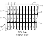
ディスプレイパネル用のカラーフィルタの製造には、種々の異なる空間パターンを有するイメージングカラー要素を含むことができる。「ストライプパターン」と呼ばれる1つの特定パターンが、図2−Aのカラーフィルタ10に示されている。カラーフィルタ10は基板18を含み、基板18には、赤カラー要素R、緑カラー要素G及び青カラー要素Bの細長ストライプ(列)12,14,16が交互にイメージングされている。個々のカラー要素R,G,Bは、不透明なマトリクス層20により境界を定められている。図2−Aの例では、マトリクス層20は、個々のカラー要素R,G,Bの2次元マトリクスパターンの輪郭を形成し、このマトリクスパターンにおいては、カラー要素の列12,14,16がそれぞれ1色を有し、カラー要素の行13,15,17が各色を交互に有している。マトリクス20は、フラットパネルディスプレイにおいて通常用いられるバックライトがカラー要素間に漏れるのを防ぐ。図示される実施形態では、マトリクス層20は、カラーフィルタ10に関連する回路(通常は薄膜トランジスタ(TFT))をマスキングするための領域22をさらに含む。
Manufacturing color filters for display panels can include imaging color elements having a variety of different spatial patterns. One particular pattern, referred to as a “striped pattern”, is shown in the
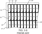
図2−Bは、「モザイクパターン」と呼ばれるカラー要素R,G,Bの別の空間パターンを有するカラーフィルタ24を示す。カラーフィルタ24のモザイク形状は、カラー要素の列12’,14’,16’と行13’,15’,17’のいずれもが各色を交互に有する個々のカラー要素R,G,Bの2次元マトリクスパターンを有する。カラーフィルタ24のモザイクパターンは、カラーフィルタ10のストライプパターンに対して改良された混色を提供できる。カラーフィルタ24のその他の特徴はカラーフィルタ10と同様である。
FIG. 2-B shows a
カラーフィルタを「デルタパターン」(図示せず)に製造することもできる。デルタパターンでは、赤、緑、青のカラー要素が互いに三角形の関係を有する空間パターンにカラー要素が形成されている。デルタパターンで製造されたカラーフィルタは、カラーフィルタのストライプパターン及びカラーフィルタ24のモザイクパターンに比べて改良された混色を提供できる。
The color filter can also be manufactured in a “delta pattern” (not shown). In the delta pattern, the color elements are formed in a spatial pattern in which the red, green, and blue color elements have a triangular relationship with each other. A color filter manufactured with a delta pattern can provide improved color mixing compared to the stripe pattern of the color filter and the mosaic pattern of the
フラットパネルディスプレイに使用されるカラーフィルタの製造に適した1タイプのイメージング装置では、染料ドナー要素が染料受け取り基板に近接して配置されている。イメージングヘッドがレーザを照射し、このレーザ照射が基板の表面を横切って走査されることにより、染料がドナー要素から受け取り基板に、画像に関連して転写される。カラーフィルタの赤、青、緑の部分は、別々のステップでイメージングしてもよい。この場合、各ステップが異なる着色染料ドナー要素を有する。このタイプのイメージング装置のイメージングヘッドは、本発明によるマルチチャネル光弁を備えることができる。 In one type of imaging device suitable for the manufacture of color filters used in flat panel displays, a dye donor element is placed proximate to the dye receiving substrate. The imaging head irradiates a laser, which is scanned across the surface of the substrate, thereby transferring dye from the donor element to the receiving substrate in relation to the image. The red, blue and green portions of the color filter may be imaged in separate steps. In this case, each step has a different colored dye donor element. The imaging head of this type of imaging device can comprise a multi-channel light valve according to the present invention.
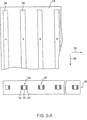
本発明の特定実施形態は、個々に変調可能な複数のチャネルを生成できる光弁を備え、これらのチャネルの2つ以上が異なる(不均一の)サイズを有する。図3−Aは、本発明の特定実施形態による光弁のチャネルパターン30を概略的に示している。光弁は、イメージングされている空間パターンに対応すべく選択された不均一のチャネルパターン30を生成するように構成されている。例えば、本発明による光弁は、離間配置されたチャネル群34、低解像度(すなわち、より大きいサイズの)チャネル32、及び高解像度(すなわち、より小さいサイズの)チャネル33を生成することができる。図3−Aに示される実施形態では、不均一チャネルパターン30は、離間して設けられた複数のチャネル群34を含み、各チャネル群34が1つの低解像度チャネル32と、この低解像度チャネル32のいずれかの側に位置する2つの高解像度チャネル33とを含む。ここで、チャネル群34、及び各チャネル群34内での低解像度チャネル32と高解像度チャネル33の配置は、基板18にイメージングされているストライプ空間パターンに一致する。
Certain embodiments of the invention comprise a light valve that can generate a plurality of individually modifiable channels, with two or more of these channels having different (non-uniform) sizes. FIG. 3A schematically illustrates a light
図3−Aは、基板18に対する赤のストライプ36の形成を概略的に示している。図示される実施形態では、チャネル群34どうしは、ストライプ36どうしの間隙に対応する距離を隔てて互いに配置されている。ただし、(以下にさらに説明するように)この間隙は必須ではない。各群34において、低解像度チャネル32がストライプ36の内部部分(端部から遠位部分)に対応し、高解像度チャネル33がストライプ36の端部に対応する。低解像度チャネル32がストライプ36の比較的大きい内部部分のイメージングを可能にし、高解像度チャネル33により、ストライプ36が良好なエッジ鮮明度を有することが確実になる。特に、高解像度チャネル33を含むことにより、ストライプ36の幅を、媒体(すなわち、基板18)または基板18上のイメージストライプ36に影響し得る他の条件に適するように正確に調整できる。さらに、低解像度チャネル32と高解像度チャネル33との組み合わせにより、結果として得られるイメージパターンをある範囲内で調整できる柔軟性を残しつつ、固定したマスク光弁によるイメージングを提供できる。
FIG. 3A schematically illustrates the formation of
図3−Aの実施形態においては、チャネルパターン30を矢印38で示されるメイン走査方向に走査することにより、ストライプ36が基板18にイメージングされる。メイン走査方向38における各パスの後、チャネルパターン30が、基板18に対し、矢印39で示されるサブ走査方向に進められる(ステッピングされる)。その後、新たなパスがメイン走査方向38に開始され、基板18の所望領域全体がイメージングされるまでこの処理が繰り返される。
In the embodiment of FIG. 3A, the
図3−Bには、前の処理部分(図3−A)において赤のストライプ36がイメージングされた後の緑のストライプ40のイメージングが概略的に示されている。図3−Bは、緑のストライプ40の意図される位置に一致するべく、チャネルパターン30のスタート位置が赤のストライプ36のイメージングに用いるスタート位置に対してサブ走査方向39にずらされていることを示している。それ以外の点については、緑のストライプ40のイメージングは、赤のストライプ36のイメージングと実質的に同様である。緑のストライプ40の後、青のストライプ(図示せず)を実質的に同様の処理でイメージングすることができる。
FIG. 3B schematically illustrates the imaging of the
図4は、本発明の特定実施形態による光弁57を示す。光弁57は、図3−A及び図3−Bのチャネルパターン30と同様のチャネルパターンを生成すべく構成されている。図4の実施形態の光弁57は、シリコン基板52上に形成された複数の窒化ケイ素リボン要素50を含む。各リボン要素50に対応する溝が基板52の上部表面にエッチングされている。また、基板材料をリボン要素50の下部からエッチングにより取り除くことで、リボン要素50が基板52において穴(図示せず)の上方に懸架した状態になる。各リボン要素50は金属材料56で被覆され、これが、電極及び反射層のいずれとしても機能する。光弁57は、基板52の下側部に共通電極を含み、この共通電極がシステム接地に接続される。
FIG. 4 shows a
光弁57は、複数のワイヤボンド接続60を含み、そのそれぞれが対応するリボン要素50の電極56に接続されている。光弁57は、さらに、複数のドライバ58を含み、これらのドライバ58がワイヤボンド接続60に電気的に接続されている。図示される実施形態においては、各ドライバ58は、1群の接続部60と、対応するリボン要素50群とに電気的に接続されている。光弁57の異なるリボン要素群が、異なる(不均一の)数の個別リボン要素50を含むことが効果的である。例えば、リボン要素群133Aは、すべてがドライバ58Aに電気的に接続された4つの個別リボン要素50を含み、リボン要素群132Bは、全てがドライバ58Bに電気的に接続された16の個別リボン要素50を含み、リボン要素群133Cは、すべてがドライバ58Cに電気的に接続された4つの個別リボン要素50を含む。
The
光弁57の動作は、(図1に)示され、すでに記載され、米国特許第6,147,789号にさらに詳細に説明される光弁100と同様である。リボン要素50の電極56に電圧が印加されると、電極56と共通電極62とのあいだに発生した静電力により、対応するリボン要素50が穴の内部に向かって変形し、これによって湾曲したミラーを形成する。上述したように、リボン要素がこのように変形すると、その反射面に入射した光線は集束され、この結果、ストップの透過領域を通過して透過し、基板をイメージングする。
The operation of the
ただし、本発明によれば、不均一な数の個別光弁要素を有する光弁要素群を、単一のドライバによって同時に駆動できる。例えば、ドライバ58Aは、要素群133Aの4つの個別リボン要素50の電極56に電圧を印加して、この要素群133Aの個別リボン要素50を変形させることができる。同様に、ドライバ58Bは、要素群132Bの個別リボン要素50の電極に独立的に電圧を印加し、この要素群132Bのリボン要素を変形させることができる。
However, according to the present invention, a group of light valve elements having a non-uniform number of individual light valve elements can be simultaneously driven by a single driver. For example, the
光弁57をイメージングヘッド(例えば、図1のイメージングヘッド115)において使用し、チャネルパターン30の高解像度チャネル33及び低解像度チャネル32(図3−A)と同様の高解像度チャネルと低解像度チャネルとを有するチャネルパターンを生成することができる。当業者であれば、より少数の個別リボン要素50を有するリボン要素群(例えば、群133A及び133C)を使用して高解像度チャネルを生成でき、より多数の個別リボン要素50を有するリボン要素群(例えば、群132B)を使用して低解像度チャネルを生成できることが理解できるであろう。単一のドライバ58に接続されている各リボン要素50群を、光弁57のチャネルと呼ぶことができる。したがって、光弁57は不均一のチャネルを複数含み、光弁57のより小さい(高解像度の)チャネルは、より少数の個別リボン要素50を有するリボン要素群に対応し、光弁57のより大きい(低解像度の)チャネルは、より多数の個別リボン要素50を有するリボン要素群に対応すると言える。
The
解像度の要件、イメージングされる媒体、イメージングされるパターン、及び個別リボン要素の大きさに応じて、光弁57は、より多数または少数の個別リボン要素50を有するチャネル(すなわち、リボン要素群)、あるいは単一の個別リボン要素50を含むことができる。かかるリボン要素群は、それぞれ独立して単一のドライバにより駆動できる。
Depending on the resolution requirements, the media being imaged, the pattern being imaged, and the size of the individual ribbon elements, the
本発明による光弁は、種々の光弁要素群の空間的配置及び各光弁要素群における個々の光弁要素の数が、イメージングされている空間パターンに一致すべく選択可能に構成できる。例えば、図4の光弁57は、相対的に少数の個別リボン要素50を有するリボン要素群133A及び133Cを、相対的に多数の個別リボン要素50を有するリボン要素群132Bの外側に有している。このようなリボン要素群の配置により、より大型の低解像度チャネルの外側に位置するより小型の高解像チャネルを生成することができ、すでに説明したように、この構成はストライプパターン、例えば図2−Aのストライプパターン、及び図3−A及び図3−Bのストライプ36及び40のイメージングに非常に適している。当業者であれば、リボン要素群のこの同じ構成が、モザイクパターン、例えば図2−Bのモザイクパターンにも非常に適することがわかるであろう。
The light valves according to the present invention can be configured such that the spatial arrangement of the various light valve element groups and the number of individual light valve elements in each light valve element group can be selected to match the spatial pattern being imaged. For example, the
本発明による光弁は、イメージングされている空間パターンにさらに対応するように互いに離間して設けられたチャネル(すなわち、光弁要素群)をさらに含む。例えば、光弁57は、互いに距離135を隔てて離間配置されたリボン要素群134Aと134Bとを含む。このようなリボン要素群の離間配置により、対応する間隔で離間して設けられた不均一サイズのチャネル群、例えば図3−Aのリボン要素群34を生成することができる。上述のように、このように離間して設けられた不均一サイズのチャネル群34は、離間して設けられた複数の特徴を有するパターン、例えば図3−A及び図3−Bの離間したストライプ36及び40のイメージングに非常に適している。当業者であれば、リボン要素間の間隙も不均一であってよいことがわかるであろう。
The light valve according to the present invention further includes channels (i.e., light valve element groups) spaced apart from one another to further correspond to the spatial pattern being imaged. For example, the
光弁57の不均一形状は、光弁が提供できる解像度のために、相対的に少数のドライバ58を含む。より詳細には、相対的に多数の個別リボン要素50を有するリボン要素群(すなわち、低解像度チャネルに対応するリボン要素群)が、単一ドライバに接続される。したがって、特定パターン、例えば図3−Aのストライプパターンのイメージングのために、光弁57は、少数の個別リボン要素50を有するリボン要素群(すなわち、高解像度チャネルに対応するリボン要素群)に関連する解像度を、より少数のドライバを用いて提供することができる。このようにドライバの数が低減するため、本発明による光弁においては、ドライバに基づく制限、例えば、スペーシングの要件、熱除去の要件、及び電気的接続の要件による制限が緩くなる。
The non-uniform shape of the
光弁57の特定形状(すなわち、低解像度チャネル132Bの外側に1つ以上の高解像度チャネル133A及び133Cを有する形状)は、本発明による不均一光弁の単なる1例を示しているにすぎない。上述のように、光弁57は、図2−Aのストライプパターン及び図2−Bのモザイクパターンのイメージングに非常に適している。当業者であれば、不均一のチャネル(すなわち、不均一数の個別光弁要素を有する光弁要素群)を有する光弁を使用して種々の異なるチャネルパターンが生成でき、ここで説明したストライプパターンに限定されないことがわかるであろう。あるイメージングパターンにおける特徴の規則性を認識するに際し、本発明の光弁は、所与数の光弁要素及び所与数のドライバに対していっそうのイメージング性能を提供する。本発明によれば、不均一な数の個別光弁要素を有する個々に変調可能な光弁要素群を含む不均一光弁を、イメージングされる空間パターンに低解像度の特徴の認識可能なパターンが含まれるどんな場合にも使用することができる。
The particular shape of the light valve 57 (ie, the shape having one or more
本発明の実施形態は、一般に、マルチチャネル光弁を含むいかなるイメージング装置にも適用可能である。さらに、本発明の実施形態は、フラットパネルディスプレイ用のカラーフィルタ製造方法のみならず、イメージングに関する他の多くの処理にも適用できる。イメージングに関する他の処理の限定的でない例には、半導体装置の製造及び「ラブオンチップ(Lab-on-a-chip)」製造のための生物医学イメージングを含む。 Embodiments of the present invention are generally applicable to any imaging device that includes a multi-channel light valve. Furthermore, the embodiment of the present invention can be applied not only to a color filter manufacturing method for a flat panel display but also to many other processes related to imaging. Non-limiting examples of other processes related to imaging include semiconductor device manufacturing and biomedical imaging for “Lab-on-a-chip” manufacturing.
前述の開示に鑑みて当業者には明らかなように、本発明の実施においては、その範囲を逸脱することなく多くの変更及び修正が可能である。以下に例を示す。
図4の実施形態における光弁57では、リボン要素50群は、イメージングされるパターンに対応する離間した位置に製造されている。例えば、群134Aは、群134Bから離間した位置に生成されている。別の実施形態では、光弁は、均一間隔で配置された複数のリボン要素を有するように製造され、要素群134A及び134Bは、その後、所望のリボン要素を所望のドライバに接続し、その他のリボン要素を接続しないでおくことにより形成される。例えば、均一間隔で配置されたリボン要素を有する光弁において、スペース135に位置するリボン要素はいずれも接続されないままにしてもよい。実際には、多くの光弁がまず接続部を設けずに製造され、続いて、ワイヤボンディングにより接続が行われる。本発明の光弁は、このように、基板上に製造し、その後、イメージングされるパターン(同様パターンの範囲)に応じて種々の光弁要素群を接続することにより構成される。
実施形態によっては、本発明による光弁は、不均一な数の個別光弁要素を有する光弁要素群に加え、あるいはこれらの要素群に代えて、不均一なサイズを有する光弁要素を含んでもよい。
他の光弁ベースのイメージングヘッドが当業界で知られている。これらのイメージングヘッドの光弁は、種々の代替技術を利用して、基板のイメージングに使用できる個別に変調可能な複数のチャネルを提供する。代替光弁の限定的でない例には、例えば、米国特許第5,517,359号に開示されているようなPLZT(チタン酸ジルコン酸ランタン鉛: lead lanthanum zirconate titanate)光弁、米国特許第6,169,565号に開示されているようなTIR(全反射)光弁、及び米国特許第5,611,592号に開示されているような格子光弁を含む。当業者であれば、本発明が、これらまたは別のタイプの他の光弁を使用して、また、これらまたは別のタイプの他の光弁を組み込んだイメージング装置において実施可能であることがわかるであろう。
上記の光弁の特定実施形態は、変形することによって湾曲したミラーまたは平坦なミラーを形成することができるリボン要素を含む。当業者であれば、本発明が、ミラータイプのリボン要素に代えて別の光弁要素を含む他のタイプの光弁に適用できることがわかるであろう。例えば、本発明による光弁は、レンズタイプの光弁要素または格子タイプの光弁要素を含んでもよい。本発明による光弁は、いかなるタイプの光弁要素を組み込んでもよい。
上記の好ましい実施形態では、不均一な数の個別光弁要素を有する光弁要素群が単一のドライバに電気的に接続されている。実施形態によっては、不均一な数の光弁要素を有する光弁要素群は、複数のドライバに電気的に接続されている。これら複数のドライバを同時に駆動し、1つの光弁要素群の個々の光弁要素をほぼ同時に駆動してもよい。
このように、本発明の範囲は、以下のクレイムによって定められる内容にしたがって解釈すべきである。
As will be apparent to those skilled in the art in view of the foregoing disclosure, many changes and modifications may be made in the practice of the invention without departing from the scope thereof. An example is shown below.
In the
In some embodiments, a light valve according to the present invention includes a light valve element having a non-uniform size in addition to or instead of a light valve element group having a non-uniform number of individual light valve elements. But you can.
Other light valve based imaging heads are known in the art. These imaging head light valves utilize a variety of alternative techniques to provide a plurality of individually modifiable channels that can be used to image the substrate. Non-limiting examples of alternative light valves include, for example, a PLZT (lead lanthanum zirconate titanate) light valve, US Pat. No. 6,517,359, as disclosed in US Pat. No. 5,517,359. , 169,565 and a grating light valve as disclosed in US Pat. No. 5,611,592. One skilled in the art will appreciate that the present invention can be practiced using other light valves of these or other types and in imaging devices incorporating these or other types of light valves. Will.
Certain embodiments of the light valve described above include a ribbon element that can be deformed to form a curved or flat mirror. One skilled in the art will appreciate that the present invention is applicable to other types of light valves that include other light valve elements instead of mirror type ribbon elements. For example, a light valve according to the present invention may comprise a lens type light valve element or a grating type light valve element. The light valve according to the present invention may incorporate any type of light valve element.
In the preferred embodiment described above, a group of light valve elements having a non-uniform number of individual light valve elements are electrically connected to a single driver. In some embodiments, the light valve element group having a non-uniform number of light valve elements is electrically connected to the plurality of drivers. The plurality of drivers may be driven simultaneously, and the individual light valve elements of one light valve element group may be driven almost simultaneously.
Thus, the scope of the present invention should be construed in accordance with the content defined by the following claims.
Claims (3)
前記チャネルの少なくとも2つが不均一なサイズを有し、該不均一なサイズが、イメージングされる規則的パターンに対応する、光弁。A light valve used in an imaging system, which includes a plurality of channels that are element groups composed of a plurality of light valve elements, and each channel is driven by an input signal of a single driver independently of each other channel. it is possible to, in response to the drive, the light received from the light source is reflected, and outputs the light as rays, light rays said output and said plurality of channels have a non-uniform size,
A light valve wherein at least two of the channels have a non-uniform size, the non-uniform size corresponding to a regular pattern to be imaged .
Applications Claiming Priority (2)
| Application Number | Priority Date | Filing Date | Title |
|---|---|---|---|
| US10/628,887 US7042624B2 (en) | 2003-07-29 | 2003-07-29 | Non-uniform light valve |
| PCT/CA2004/001410 WO2005012976A1 (en) | 2003-07-29 | 2004-07-28 | Non-uniform light valve |
Publications (3)
| Publication Number | Publication Date |
|---|---|
| JP2007500366A JP2007500366A (en) | 2007-01-11 |
| JP2007500366A5 JP2007500366A5 (en) | 2007-09-13 |
| JP4533377B2 true JP4533377B2 (en) | 2010-09-01 |
Family
ID=34103473
Family Applications (1)
| Application Number | Title | Priority Date | Filing Date |
|---|---|---|---|
| JP2006521358A Expired - Fee Related JP4533377B2 (en) | 2003-07-29 | 2004-07-28 | Uneven light valve |
Country Status (8)
| Country | Link |
|---|---|
| US (1) | US7042624B2 (en) |
| EP (1) | EP1664897B1 (en) |
| JP (1) | JP4533377B2 (en) |
| KR (1) | KR101045703B1 (en) |
| CN (1) | CN100434960C (en) |
| AT (1) | ATE511118T1 (en) |
| TW (1) | TW200530625A (en) |
| WO (1) | WO2005012976A1 (en) |
Families Citing this family (4)
| Publication number | Priority date | Publication date | Assignee | Title |
|---|---|---|---|---|
| KR100712215B1 (en) | 2005-08-25 | 2007-04-27 | 삼성에스디아이 주식회사 | Mask for LITI and LITI method using the same |
| KR20090034351A (en) * | 2006-07-28 | 2009-04-07 | 코닥 그래픽 커뮤니케이션즈 캐나다 캄파니 | Enhanced imaging of features |
| JP2011511312A (en) * | 2008-01-30 | 2011-04-07 | コダック グラフィック コミュニケーションズ カナダ カンパニー | Image formation of feature patterns with distorted edges |
| US8436882B2 (en) * | 2008-01-30 | 2013-05-07 | Kodak Graphic Communications Canada Company | Imaging features with skewed edges |
Family Cites Families (10)
| Publication number | Priority date | Publication date | Assignee | Title |
|---|---|---|---|---|
| US4374397A (en) * | 1981-06-01 | 1983-02-15 | Eastman Kodak Company | Light valve devices and electronic imaging/scan apparatus with locationally-interlaced optical addressing |
| US4965242A (en) * | 1989-12-11 | 1990-10-23 | Eastman Kodak Company | Method of making color filter array for liquid crystal display |
| US5049901A (en) * | 1990-07-02 | 1991-09-17 | Creo Products Inc. | Light modulator using large area light sources |
| WO1997034171A2 (en) * | 1996-02-28 | 1997-09-18 | Johnson Kenneth C | Microlens scanner for microlithography and wide-field confocal microscopy |
| US6143451A (en) * | 1996-11-26 | 2000-11-07 | E. I. Du Pont De Nemours And Company | Imaged laserable assemblages and associated processes with high speed and durable image-transfer characteristics for laser-induced thermal transfer |
| US6271957B1 (en) * | 1998-05-29 | 2001-08-07 | Affymetrix, Inc. | Methods involving direct write optical lithography |
| JP3706264B2 (en) * | 1998-12-21 | 2005-10-12 | 日本放送協会 | Projection type multi-screen display device |
| US6188519B1 (en) * | 1999-01-05 | 2001-02-13 | Kenneth Carlisle Johnson | Bigrating light valve |
| JP4308467B2 (en) * | 2001-12-27 | 2009-08-05 | 新光電気工業株式会社 | Exposure method and exposure apparatus |
| US6728023B1 (en) * | 2002-05-28 | 2004-04-27 | Silicon Light Machines | Optical device arrays with optimized image resolution |
-
2003
- 2003-07-29 US US10/628,887 patent/US7042624B2/en not_active Expired - Fee Related
-
2004
- 2004-07-28 KR KR1020067001937A patent/KR101045703B1/en not_active IP Right Cessation
- 2004-07-28 JP JP2006521358A patent/JP4533377B2/en not_active Expired - Fee Related
- 2004-07-28 AT AT04738017T patent/ATE511118T1/en not_active IP Right Cessation
- 2004-07-28 WO PCT/CA2004/001410 patent/WO2005012976A1/en active Application Filing
- 2004-07-28 EP EP04738017A patent/EP1664897B1/en not_active Not-in-force
- 2004-07-28 CN CNB2004800282977A patent/CN100434960C/en not_active Expired - Fee Related
- 2004-07-29 TW TW093122710A patent/TW200530625A/en unknown
Also Published As
| Publication number | Publication date |
|---|---|
| CN1860401A (en) | 2006-11-08 |
| KR101045703B1 (en) | 2011-06-30 |
| EP1664897A1 (en) | 2006-06-07 |
| US20050024706A1 (en) | 2005-02-03 |
| CN100434960C (en) | 2008-11-19 |
| ATE511118T1 (en) | 2011-06-15 |
| WO2005012976A1 (en) | 2005-02-10 |
| JP2007500366A (en) | 2007-01-11 |
| EP1664897A4 (en) | 2008-03-12 |
| US7042624B2 (en) | 2006-05-09 |
| EP1664897B1 (en) | 2011-05-25 |
| KR20060128818A (en) | 2006-12-14 |
| TW200530625A (en) | 2005-09-16 |
Similar Documents
| Publication | Publication Date | Title |
|---|---|---|
| KR101084417B1 (en) | Method for imaging regular patterns | |
| US6728023B1 (en) | Optical device arrays with optimized image resolution | |
| US8330783B2 (en) | Imaging patterns of features with skewed edges | |
| US8305409B2 (en) | Forming an image with a plurality of imaging heads | |
| US8233020B2 (en) | Enhanced imaging of features | |
| US8436882B2 (en) | Imaging features with skewed edges | |
| JP4533377B2 (en) | Uneven light valve | |
| US20100238260A1 (en) | Bidirectional imaging with varying intensities | |
| US20090309954A1 (en) | Methods and apparatus for selecting and applying non-contiguous features in a pattern | |
| TW200949309A (en) | Imaging patterns of features with varying resolutions |
Legal Events
| Date | Code | Title | Description |
|---|---|---|---|
| A521 | Request for written amendment filed |
Free format text: JAPANESE INTERMEDIATE CODE: A523 Effective date: 20070724 |
|
| A621 | Written request for application examination |
Free format text: JAPANESE INTERMEDIATE CODE: A621 Effective date: 20070724 |
|
| A131 | Notification of reasons for refusal |
Free format text: JAPANESE INTERMEDIATE CODE: A131 Effective date: 20091020 |
|
| A521 | Request for written amendment filed |
Free format text: JAPANESE INTERMEDIATE CODE: A523 Effective date: 20100114 |
|
| A131 | Notification of reasons for refusal |
Free format text: JAPANESE INTERMEDIATE CODE: A131 Effective date: 20100202 |
|
| A521 | Request for written amendment filed |
Free format text: JAPANESE INTERMEDIATE CODE: A523 Effective date: 20100427 |
|
| TRDD | Decision of grant or rejection written | ||
| A01 | Written decision to grant a patent or to grant a registration (utility model) |
Free format text: JAPANESE INTERMEDIATE CODE: A01 Effective date: 20100518 |
|
| A01 | Written decision to grant a patent or to grant a registration (utility model) |
Free format text: JAPANESE INTERMEDIATE CODE: A01 |
|
| A61 | First payment of annual fees (during grant procedure) |
Free format text: JAPANESE INTERMEDIATE CODE: A61 Effective date: 20100611 |
|
| R150 | Certificate of patent or registration of utility model |
Ref document number: 4533377 Country of ref document: JP Free format text: JAPANESE INTERMEDIATE CODE: R150 Free format text: JAPANESE INTERMEDIATE CODE: R150 |
|
| FPAY | Renewal fee payment (event date is renewal date of database) |
Free format text: PAYMENT UNTIL: 20130618 Year of fee payment: 3 |
|
| R250 | Receipt of annual fees |
Free format text: JAPANESE INTERMEDIATE CODE: R250 |
|
| R250 | Receipt of annual fees |
Free format text: JAPANESE INTERMEDIATE CODE: R250 |
|
| R250 | Receipt of annual fees |
Free format text: JAPANESE INTERMEDIATE CODE: R250 |
|
| R250 | Receipt of annual fees |
Free format text: JAPANESE INTERMEDIATE CODE: R250 |
|
| R250 | Receipt of annual fees |
Free format text: JAPANESE INTERMEDIATE CODE: R250 |
|
| S531 | Written request for registration of change of domicile |
Free format text: JAPANESE INTERMEDIATE CODE: R313531 |
|
| S111 | Request for change of ownership or part of ownership |
Free format text: JAPANESE INTERMEDIATE CODE: R313111 |
|
| R350 | Written notification of registration of transfer |
Free format text: JAPANESE INTERMEDIATE CODE: R350 |
|
| R350 | Written notification of registration of transfer |
Free format text: JAPANESE INTERMEDIATE CODE: R350 |
|
| R250 | Receipt of annual fees |
Free format text: JAPANESE INTERMEDIATE CODE: R250 |
|
| LAPS | Cancellation because of no payment of annual fees |