JP4530527B2 - Static semiconductor memory device - Google Patents
Static semiconductor memory device Download PDFInfo
- Publication number
- JP4530527B2 JP4530527B2 JP2000374261A JP2000374261A JP4530527B2 JP 4530527 B2 JP4530527 B2 JP 4530527B2 JP 2000374261 A JP2000374261 A JP 2000374261A JP 2000374261 A JP2000374261 A JP 2000374261A JP 4530527 B2 JP4530527 B2 JP 4530527B2
- Authority
- JP
- Japan
- Prior art keywords
- power supply
- memory cell
- level
- column
- switching element
- Prior art date
- Legal status (The legal status is an assumption and is not a legal conclusion. Google has not performed a legal analysis and makes no representation as to the accuracy of the status listed.)
- Expired - Lifetime
Links
- 239000004065 semiconductor Substances 0.000 title claims description 34
- 230000003068 static effect Effects 0.000 title claims description 18
- 230000015654 memory Effects 0.000 claims description 153
- 230000002950 deficient Effects 0.000 claims description 26
- 238000000034 method Methods 0.000 claims description 18
- 239000000758 substrate Substances 0.000 claims description 16
- 230000004044 response Effects 0.000 claims description 15
- 238000010586 diagram Methods 0.000 description 24
- 238000003860 storage Methods 0.000 description 16
- 229910052751 metal Inorganic materials 0.000 description 10
- 239000002184 metal Substances 0.000 description 10
- 239000000463 material Substances 0.000 description 7
- XUIMIQQOPSSXEZ-UHFFFAOYSA-N Silicon Chemical compound [Si] XUIMIQQOPSSXEZ-UHFFFAOYSA-N 0.000 description 5
- 229910052710 silicon Inorganic materials 0.000 description 5
- 239000010703 silicon Substances 0.000 description 5
- 230000000694 effects Effects 0.000 description 4
- 229910052782 aluminium Inorganic materials 0.000 description 3
- XAGFODPZIPBFFR-UHFFFAOYSA-N aluminium Chemical compound [Al] XAGFODPZIPBFFR-UHFFFAOYSA-N 0.000 description 3
- 239000003990 capacitor Substances 0.000 description 3
- 238000005520 cutting process Methods 0.000 description 2
- 230000007257 malfunction Effects 0.000 description 2
- 230000004048 modification Effects 0.000 description 2
- 238000012986 modification Methods 0.000 description 2
- 229910021420 polycrystalline silicon Inorganic materials 0.000 description 2
- 229920005591 polysilicon Polymers 0.000 description 2
- GAAKALASJNGQKD-UHFFFAOYSA-N LY-165163 Chemical compound C1=CC(N)=CC=C1CCN1CCN(C=2C=C(C=CC=2)C(F)(F)F)CC1 GAAKALASJNGQKD-UHFFFAOYSA-N 0.000 description 1
- 230000004913 activation Effects 0.000 description 1
- 238000007664 blowing Methods 0.000 description 1
- 230000007423 decrease Effects 0.000 description 1
- 230000007547 defect Effects 0.000 description 1
- 230000003111 delayed effect Effects 0.000 description 1
- 238000004519 manufacturing process Methods 0.000 description 1
- 239000000126 substance Substances 0.000 description 1
Images


Classifications
-
- G—PHYSICS
- G11—INFORMATION STORAGE
- G11C—STATIC STORES
- G11C29/00—Checking stores for correct operation ; Subsequent repair; Testing stores during standby or offline operation
- G11C29/70—Masking faults in memories by using spares or by reconfiguring
- G11C29/78—Masking faults in memories by using spares or by reconfiguring using programmable devices
- G11C29/785—Masking faults in memories by using spares or by reconfiguring using programmable devices with redundancy programming schemes
Description
【0001】
【発明の属する技術分野】
この発明はスタティック型半導体記憶装置に関し、特に、不良な行または列をスペア行または列で置換する冗長方式が採用されたスタティック型半導体記憶装置に関する。
【0002】
【従来の技術】
図10は、従来のスタティックランダムアクセスメモリ(以下、SRAMと称す)の構成を示す回路ブロック図である。
【0003】
図10において、このSRAMは、複数行複数列(図では4行4列)に配置された複数のメモリセルMCと、各行に対応して設けられたワード線WLと、各列に対応して設けられたビット線対BL,/BLとを備える。
【0004】
また、このSRAMは、各ビット線対BL,/BLに対応して設けられ、対応のビット線対BL,/BLを「H」レベルに充電するためのビット線負荷31,32と、データ入出力線対IO,/IOと、各ビット線対BL,/BLに対応して設けられ、対応のビット線対BL,/BLとデータ入出力線対IO,/IOとを接続するための列選択ゲート33と、各ビット線対BL,/BLに対応して設けられた列選択線CSLとを備える。
【0005】
ビット線負荷31,32は、それぞれ電源電位VDDのラインとビット線BL,/BLの一方端との間に接続され、各々のゲートがともに接地電位VSSのラインに接続された1対のPチャネルMOSトランジスタを含む。列選択ゲート33は、それぞれビット線BL,/BLの他方端とデータ入出力線IO,/IOの一方端との間に接続され、各々のゲートがともに列選択線CSLを介して列デコーダ37に接続された1対のNチャネルMOSトランジスタを含む。
【0006】
さらに、このSRAMは、行デコーダ34、制御回路36、列デコーダ37、書込回路38、および読出回路39を備える。行デコーダ34は、外部から与えられる行アドレス信号に従って複数のワード線WLのうちのいずれかのワード線WLを選択し、そのワード線WLを非選択レベルの「L」レベルから選択レベルの「H」レベルに立上げる。行デコーダ34は、各ワード線WLに対応して設けられ、対応のワード線WLを非選択レベルの「L」レベルにするためのNチャネルMOSトランジスタ35を含む。図10では、各NチャネルMOSトランジスタ35のゲートに電源電位VDDが与えられ、各ワード線WLが対応のNチャネルMOSトランジスタ35を介して接地されている状態が示される。制御回路36は、外部から与えられる制御信号に従ってSRAM全体を制御する。列デコーダ37は、外部から与えられる列アドレス信号に従って複数の列選択線CSLのうちのいずれかの列選択線CSLを選択し、その列選択線CSLを非選択レベルの「L」レベルから選択レベルの「H」レベルに立上げる。
【0007】
書込回路38および読出回路39は、ともにデータ入出力線対IO,/IOの他方端に接続される。書込回路38は、外部から与えられたデータDIを行デコーダ34および列デコーダ37によって選択されたメモリセルMCに書込む。読出回路39は、行デコーダ34および列デコーダ37によって選択されたメモリセルMCからの読出データDOを外部に出力する。
【0008】
次に、図10に示したSRAMの動作について説明する。書込動作時は、行アドレス信号に対応する行のワード線WLが行デコーダ34によって選択レベルの「H」レベルに立上げられ、その行の各メモリセルMCが活性化される。次いで、列アドレス信号に対応する列の列選択線CSLが列デコーダ37によって選択レベルの「H」レベルに立上げられ、その列の活性化されたメモリセルMCがビット線対BL,/BL、列選択ゲート33およびデータ入出力線対IO,/IOを介して書込回路38に接続される。
【0009】
書込回路38は、外部から与えられたデータDIに従ってデータ入出力線対IO,/IOのうちの一方を「H」レベルにするとともに他方を「L」レベルにし、活性化されたメモリセルMCにデータDIを書込む。ワード線WLおよび列選択線CSLが非選択レベルの「L」レベルに立下げられると、そのメモリセルMCにデータが記憶される。
【0010】
読出動作時は、列アドレス信号に対応する列の列選択線CSLが列デコーダ37によって選択レベルの「H」レベルに立上げられ、その列の各メモリセルMCがビット線対BL,/BL、列選択ゲート33およびデータ入出力線対IO,/IOを介して読出回路39に接続される。次いで、行アドレス信号に対応する行のワード線WLが行デコーダ34によって選択レベルの「H」レベルに立上げられ、その行の各メモリセルMCが活性化される。これにより、デコーダ37,34によって選択されたメモリセルMCが記憶しているデータに応じてビット線対BL,/BLのうちの一方からそのメモリセルMCに電流が流入し、データ入出力線対IO,/IOのうちの一方の電位が低下する。読出回路39は、データ入出力線IOと/IOの電位を比較し、比較結果に応じたデータDOを外部に出力する。
【0011】
図11(a)はメモリセルMCの構成を示す回路図である。図11(a)において、このメモリセルMCは、負荷トランジスタ(PチャネルMOSトランジスタ)41,42、ドライバトランジスタ(NチャネルMOSトランジスタ)43,44およびアクセストランジスタ(NチャネルMOSトランジスタ)45,46を含む。PチャネルMOSトランジスタ41,42は、それぞれメモリセル電源配線MVLと記憶ノードN1,N2との間に接続され、各々のゲートはそれぞれノードN2,N1に接続される。メモリセル電源配線MVLには、電源電位VDDが供給される。NチャネルMOSトランジスタ43,44は、それぞれ記憶ノードN1,N2とメモリセル接地配線MGLとの間に接続され、各々のゲートはそれぞれノードN2,N1に接続される。NチャネルMOSトランジスタ45,46は、それぞれ記憶ノードN1,N2とビット線BL,/BLとの間に接続され、各々のゲートはともにワード線WLに接続される。
【0012】
書込動作時は、書込データDIに応じてビット線BL,/BLのうちの一方が「H」レベルにされるとともに他方が「L」レベルにされる。次いで、ワード線WLが選択レベルの「H」レベルにされてNチャネルMOSトランジスタ45,46が導通し、ビット線BL,/BLのレベルがそれぞれ記憶ノードN1,N2に与えられる。記憶ノードN1,N2にそれぞれ「H」レベルおよび「L」レベルが与えられた場合は、MOSトランジスタ41,44が導通するとともにMOSトランジスタ42,43が非導通になり、記憶ノードN1,N2のレベルがMOSトランジスタ41〜44によってラッチされる。また、記憶ノードN1,N2にそれぞれ「L」レベルおよび「H」レベルが与えられた場合は、MOSトランジスタ42,43が導通するとともにMOSトランジスタ41,44が非導通になり、記憶ノードN1,N2のレベルがMOSトランジスタ41〜44によってラッチされる。ワード線WLが非選択レベルの「L」レベルにされると、NチャネルMOSトランジスタ45,46が非導通になって、記憶ノードN1,N2のレベルが保持される。
【0013】
読出動作時は、図10のビット線負荷31,32によってビット線BL,/BLの各々が「H」レベルに充電される。ワード線WLが選択レベルの「H」レベルにされると、NチャネルMOSトランジスタ45,46が導通する。記憶ノードN1,N2にそれぞれ「H」レベルおよび「L」レベルがラッチされている場合は、ビット線/BLからNチャネルMOSトランジスタ46,44を介してメモリセル接地線MGLに電流が流出し、ビット線BL,/BLはそれぞれ「H」レベルおよび「L」レベルになる。また、記憶ノードN1,N2にそれぞれ「L」レベルおよび「H」レベルがラッチされている場合は、ビット線BLからNチャネルMOSトランジスタ45,43を介してメモリセル接地線MGLに電流が流出し、ビット線BL,/BLがそれぞれ「L」レベルおよび「H」レベルになる。ビット線BLと/BLのレベルを比較することにより、メモリセルMCの記憶データが読出される。ワード線WLが非選択レベルの「L」レベルにされると、NチャネルMOSトランジスタ45,46が非導通になってデータの読出が終了する。
【0014】
図11(b)は、メモリセルMCのレイアウトを示す図である。シリコン基板の表面に、図中Y方向に延在する2本のゲート電極GE1,GE2が平行に形成されるとともに、図中X方向に延在するワード線WLが形成される。ゲート電極GE1,GE2およびワード線WLは、ポリシリコン層で形成される。ゲート電極GE1,GE2の一方端部の一方側から他方側にかけてそれぞれP型活性層PA1,PA2が形成される。ゲート電極GE1の他方端部の一方側から他方側およびワード線WLの一方端部の一方側から他方側にかけてN型活性層NA1が形成される。ゲート電極GE2の他方端部の一方側から他方側およびワード線WLの他方端部の一方側から他方側にかけてN型活性層NA2が形成される。
【0015】
P型活性層PA1とゲート電極GE1、P型活性層PA2とゲート電極GE2は、それぞれPチャネルMOSトランジスタ41,42を構成する。N型活性層NA1とゲート電極GE1、N型活性層NA2とゲート電極GE2は、それぞれNチャネルMOSトランジスタ43,44を構成する。N型活性層NA1とワード線WL、N型活性層NA2とワード線WLは、それぞれNチャネルMOSトランジスタ45,46を構成する。
【0016】
次に、複数のローカル配線LLが形成される。図11(b)において、ローカル配線LLと活性層が重なっている部分では、ローカル配線LLと活性層が導通している。活性層PA1,PA2の一方端部(PチャネルMOSトランジスタ41,42のソース)は、ともにメモリセル電源配線MVLに接続される。メモリセル電源配線MVLは、ローカル配線LL1で構成されている。
【0017】
P型活性層PA1の他方端部(PチャネルMOSトランジスタ41のドレイン)は、ローカル配線LL2を介してN型活性層NA1の中央部(NチャネルMOSトランジスタ43,45のドレイン)に接続される。P型活性層PA2の他方端部(PチャネルMOSトランジスタ42のドレイン)は、ローカル配線LL3を介してN型活性層NA2の中央部(NチャネルMOSトランジスタ44,46のドレイン)に接続される。ローカル配線LL2,LL3は、それぞれコンタクトホールCH,CHを介してゲート電極GE2,GE1に接続される。
【0018】
さらに、第1アルミ配線層によって、図中Y方向に延在するビット線BL,/BLおよびメモリセル接地線MGL,MGLが平行に形成される。N型活性層NA1,NA2の一方端部(NチャネルMOSトランジスタ43,44のソース)は、それぞれコンタクトホールCH,CHを介してメモリセル接地線MGL,MGLに接続される。N型活性層NA1,NA2の他方端部(NチャネルMOSトランジスタ45,46のドレイン)は、それぞれコンタクトホールCH,CHを介してビット線BL,/BLに接続される。
【0019】
メモリセルMCの基板は、図12に示すように、トリプルウェル構造にされている。すなわち、P型シリコン基板47の表面にN+型埋込層48が形成され、さらにその表面に複数(図では3つ)のN型ウェルNWが形成され、3つのN型ウェルNWの間にそれぞれ2つのP型ウェルPWが形成される。各メモリセルMCは、隣接するN型ウェルNWおよびP型ウェルPWの表面に形成される。図10で示したP型活性層PA1,PA2は、N型ウェルNWの表面に形成され、N型活性層NA1,NA2はP型ウェルPWの表面に形成される。図12では、4行4列に配置された16個のメモリセルMCが示されている。トリプルウェル構造では、P型シリコン基板47で発生した電子−ホール対がN+型埋込層でトラップされるため、ソフトエラーの発生が抑制される。
【0020】
さて、このようなSRAMでは、製造中にメモリセルMCに異物が付着し、(1)記憶ノードN1,N2間のショート、(2)記憶ノードN1またはN2とメモリセル電源配線MVL間のショート、(3)記憶ノードN1またはN2とメモリセル接地配線MGL間のショート、(4)記憶ノードN1またはN2とワード線WL間のショート、(5)記憶ノードN1またはN2とビット線BLまたは/BL間のショート、(6)ビット線BLまたは/BLとワード線WL間のショート、(7)ワード線WLとメモリセル電源配線MVL間のショート、(8)ビット線BLまたは/BLとメモリセル接地配線MGL間のショート、(9)メモリセル電源配線MVLとメモリセル接地配線MGL間のショートが発生する場合がある。図11で示したメモリセルMCでは、ビット線BL,/BLとメモリセル接地配線MGL,MGLが平行に隣接して配置されているので、特に(8)のショートが発生しやすい。
【0021】
このようなショートが発生したメモリセルMCは正常に動作しなくなる。そこで、SRAMでは、不良なメモリセルMCを含む行または列と置換するためのスペア行または列と、不良な行または列のアドレスをプログラムするためのプログラム回路を設けておき、不良な行または列のアドレスが入力された場合は不良な行または列の代わりにスペア行または列を選択することにより、不良品を救済する冗長方式が採用されている。
【0022】
しかし、単に不良な行または列をスペア行または列と置換するだけでは、ショートした部分にリーク電流が流れ続け、スタンバイ電流が規格値をオーバーしてしまう。そこで、スタンバイ電流を低減化するため、種々の方法が提案されている。
【0023】
図13の方法では、各メモリセル行に対応してヒューズ50が設けられる。ヒューズ50は、対応の行のメモリセル電源配線MVLと電源電位VDD′のラインとの間に接続され、対応の行が不良である場合はブローされる。ヒューズ50がブローされると、上記(1)〜(4)(7)(9)のショートがある場合でも、電源電位VDD′のラインからメモリセル電源配線MVLおよび不良メモリセルのショート部分に流出する電流が遮断されるので、スタンバイ電流が低減化される。このような方法は、たとえば特開平7−230699号公報に開示されている。
【0024】
【発明が解決しようとする課題】
しかし、この方法では、ヒューズ50のブローが不十分である場合は、スタンバイ電流の低減化も不十分になるという問題があった。
【0025】
また、図14は、図13に示した方法が適用されたSRAMをより詳細に示す図である。図14において、このSRAMでは、複数列(図では64列)ごとにウェル電源配線WVLおよびウェル接地配線WGLが設けられる。各ウェル電源配線WVLは、電源電位VDDを受け、コンタクトホールCHを介して図12の各N型ウェルNWに接続される。各ウェル接地配線WGLは、接地電位VSSを受け、コンタクトホールCHを介して図12の各P型ウェルPWに接続される。これにより、MOSトランジスタの活性層PAまたはNAからウェルNWまたはPWに電流が流出するのを防止することができる。各メモリセル電源配線MVLは、ヒューズ50を介して電源電位VDD′(VDD′=VDD)のラインに接続される。電源電位VDD′用のパッドと電源電位VDD用のパッドは別々に設けられている。これは、スタンバイ電流不良の解析を容易にするためである。
【0026】
しかし、このSRAMは、ラッチアップに弱いという問題がある。すなわち、図15(a)(b)に示すように、N型ウェルNWおよびP型ウェルPWはそれぞれ抵抗素子51,52を構成する。このSRAMでは、図14で示したように、ウェル電源配線WVL,WVL間の距離およびウェル接地配線WGL,WGL間の距離が長いので、抵抗素子51,52の各々の抵抗値は大きくなっている。また、PチャネルMOSトランジスタ41のP型活性層PA1とN型ウェルNWとP型ウェルPWとでPNPバイポーラトランジスタ53が構成され、N型ウェルNWとP型ウェルPWとNチャネルMOSトランジスタ43のN型活性層NA1とでNPNバイポーラトランジスタ54が構成される。
【0027】
何らかの原因でラッチアップトリガがN型ウェルNWまたはP型ウェルPWに発生してトランジスタ53,54のベース−エミッタ間電圧が順バイアスになると、トランジスタ53のコレクタ電流は抵抗素子52(P型ウェルPW)に流入してトランジスタ54のベース−エミッタ間順バイアス電圧を増大させ、トランジスタ54のコレクタ電流もトランジスタ53のベース−エミッタ間順バイアス電圧を増大させる。これにより、電源電位VDD,VDD′のラインから接地電位VSSのラインに大電流が流れ、SRAMが破壊されてしまう。なお、ヒューズ50の抵抗値は10Ω以下と小さいので、トランジスタ53に流れる電流がヒューズ50によって制限されることはない。
【0028】
また、図16の方法では、各メモリセル行に対応してプログラム回路60および電源電位供給回路66が設けられる。プログラム回路60は、ヒューズ61、NチャネルMOSトランジスタ62,63、PチャネルMOSトランジスタ64およびキャパシタ65を含む。ヒューズ61およびNチャネルMOSトランジスタ62と、MOSトランジスタ64,63とは、それぞれ電源電位VDDのラインと接地電位VSSのラインとの間に直列接続される。MOSトランジスタ64,63のゲートは、ともにヒューズ61およびNチャネルMOSトランジスタ62間のノードN61に接続される。ノードN61に現われる信号は、このプログラム回路60の出力信号φEとなる。NチャネルMOSトランジスタ62のゲートは、NチャネルMOSトランジスタ63のドレイン(ノードN63)に接続される。キャパシタ65は、電源電位VDDのラインとノードN63との間に接続される。電源電位供給回路66は、プログラム回路60の出力ノードN61と対応のメモリセル電源配線MVLとの間に直列接続された偶数段(図では2段)のインバータ67を含む。
【0029】
ヒューズ61がブローされていない場合は、電源電位VDDがヒューズ61を介してノードN61に与えられ、信号φEが「H」レベルになってメモリセル電源配線MVLに電源電位VDDが与えられる。ヒューズ61がブローされている場合は、電源投入時にキャパシタ65を介してノードN63に電源電位VDDが与えられ、MOSトランジスタ62,64が導通するとともにMOSトランジスタ63が非導通になり、信号φEが「L」レベルになってメモリセル電源配線MGLが接地される。したがって、(1)〜(4)(7)(9)のショートがある場合でもスタンバイ電流が低減化される。このような方法は、たとえば特開平7−230699号公報に開示されている。
【0030】
しかし、この方法では、ヒューズ61のブローが不十分である場合は、信号φEが「H」レベルになってメモリセル電源配線MVLに電源電位VDDが与えられるので、スタンバイ電流の低減化が図れないという問題がある。
【0031】
また、不良な行のメモリセル電源配線MVLを接地電位VSSに固定するので、スタンバイ時に「H」レベルになる信号の信号配線と接地電位VSSにされたメモリセル電源配線MVLとがショートしている場合は、スタンバイ電流不良が発生してしまう。
【0032】
また、図17の方法では、各メモリセル列に対応してヒューズ70が設けられる。ヒューズ70は、電源電位VDDのラインとPチャネルMOSトランジスタ31,32のソースとの間に介挿され、対応の列が不良である場合はブローされる。ヒューズ70がブローされると、(5)(6)(8)のショートがある場合でも電源電位VDDのラインからPチャネルMOSトランジスタ31,32およびビット線対BL,/BLを介して不良メモリセルのショート部分に流れる電流が遮断されるので、スタンバイ電流が低減化される。
【0033】
しかし、この方法でも、ヒューズ70のブローが不十分である場合は、スタンバイ電流の低減化も不十分になるという問題があった。
【0034】
また、図18の方法では、PチャネルMOSトランジスタ31,32のゲートが接地電位VSSの代わりに信号φEを受ける。スタンバイ時は、信号φEが非活性化レベルの「H」レベルになってPチャネルMOSトランジスタ31,32が非導通になる。したがって、(5)(6)(8)のショートがある場合でも、電源電位VDDのラインからPチャネルMOSトランジスタ31,32およびビット線対BL,/BLを介してそのメモリセルMCのショート部分に流れる電流が遮断されるので、スタンバイ電流が低減化される。アクティブ時は、信号φEが活性化レベルの「L」レベルになってPチャネルMOSトランジスタ31,32が導通し、図10で示したSRAMと同じ状態になる。
【0035】
しかし、この方法では、スタンバイ時は各ビット線対BL,/BLがフローティング状態にされるので、スタンバイモードから読出モードに移行したときに各ビット線対BL,/BLを「H」レベルに充電するための時間が必要となり、読出速度が遅延するという問題がある。
【0036】
また、図13〜図18で示した方法では、(1)〜(9)のショートのうちの一部のショートがあった場合にスタンバイ電流を低減化できても、他のショートがあった場合はスタンバイ電流を低減化できないという問題があった。たとえば図13の方法では、(1)〜(4)(7)(9)のショートがあった場合はスタンバイ電流を低減化できるが、(6)のショートがある場合は「H」レベルのビット線BL,/BLから「L」レベルのワード線WLに電流がリークし、スタンバイ電流を低減化できない。また図17の方法では、(5)(6)(8)のショートがあった場合はスタンバイ電流を低減化できるが、(1)〜(4)(7)(9)のショートがあった場合はメモリセル電源配線MVLから接地電位VSSのラインに電流がリークし、スタンバイ電流を低減化できない。
【0037】
それゆえに、この発明の主たる目的は、スタンバイ電流が小さく、ラッチアップに強いスタティック型半導体記憶装置を提供することである。
【0038】
【課題を解決するための手段】
この発明に係るスタティック型半導体記憶装置は、複数行複数列に配置された複数のメモリセルと、各行に対応して設けられたワード線と、各列に対応して設けられたビット線対とを備え、不良な行または列をスペア行または列で置換する冗長方式が採用されたスタティック型半導体記憶装置であって、各ワード線に対応して設けられて対応のワード線と基準電位のラインとの間に接続され、対応のワード線が選択されていない場合に導通して対応の各メモリセルを非活性状態にするための第1のスイッチング素子と、各行または列に対応して設けられ、その一方端が対応の行または列の各メモリセルの電源ノードに接続された電源配線と、各電源配線に対応して設けられて対応の電源配線の他方端と電源電位のラインとの間に接続され、第1のスイッチング素子の導通抵抗値よりも大きな予め定められた導通抵抗値を有する第2のスイッチング素子と、各行または列に対応して設けられ、対応の行または列が不良である場合にブローされるヒューズを含み、そのヒューズがブローされたことに応じて第2のスイッチング素子を非導通にするプログラム回路とを備えたものである。
【0039】
好ましくは、電源配線およびプログラム回路は各列に対応して設けられ、スタティック型半導体記憶装置は、さらに、各ビット線に対応して設けられ、その一方電極が対応のビット線に接続されたビット線負荷素子と、各列に対応して設けられて対応の列の各ビット線負荷素子の他方電極と電源電位のラインとの間に接続された第3のスイッチング素子とを備え、プログラム回路は、ヒューズがブローされたことに応じて第2のスイッチング素子とともに第3のスイッチング素子も非導通にする。
【0040】
また好ましくは、プログラム回路は、第1のノードと第1の電位のラインとの間に接続され、リセット信号が第1のレベルから第2のレベルに変化したことに応じて導通し、第1のノードの電位を第1の電位にリセットするための第4のスイッチング素子と、第1のノードと第2の電位のラインとの間にヒューズと直列接続され、リセット信号が第2のレベルから第1のレベルに変化したことに応じて導通し、ヒューズがブローされていない場合に第1のノードを第2の電位にするための第5のスイッチング素子と、リセット信号が第2のレベルから第1のレベルに変化してから予め定められた時間だけ経過したことに応じて第1のノードの電位をラッチし、ラッチした電位が第1の電位の場合に第2のスイッチング素子を非導通にするためのラッチ回路とを含む。
【0041】
また好ましくは、さらに、第1の導電形式の半導体基板と、半導体基板の表面に形成された第2の導電形式の半導体埋込層と、半導体埋込層の表面に形成された第1の導電形式の複数の第1のウェルと、半導体埋込層の表面に複数の第1のウェルの間にそれぞれ形成された第2の導電形式の複数の第2のウェルとが設けられ、複数のメモリセルは、複数の第1のウェルおよび複数の第2のウェルの表面に形成されている。
【0042】
また好ましくは、第2のスイッチング素子は、予め定められた導通抵抗値を有するトランジスタを含む。
【0043】
また好ましくは、第2のスイッチング素子は、予め定められた導通抵抗値を有する抵抗素子と、電源配線の他方端と電源電位のラインとの間に抵抗素子と直列接続されたトランジスタとを含む。
【0044】
【発明の実施の形態】
[実施の形態1]
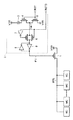
図1は、この発明の実施の形態1によるSRAMの要部を示す回路ブロック図であって、図13と対比される図である。
【0045】
図1において、このSRAMが図13のSRAMと異なる点は、ヒューズ50がPチャネルMOSトランジスタ1およびプログラム回路2で置換されている点である。PチャネルMOSトランジスタ1は、電源電位VDD′のラインと対応のメモリセル電源配線MVLとの間に接続され、そのゲートはプログラム回路2の出力信号φEを受ける。PチャネルMOSトランジスタ1は、比較的大きな予め定められた導通抵抗値(10KΩ程度以上)を有する。
【0046】
プログラム回路2は、ヒューズ3、PチャネルMOSトランジスタ4、NチャネルMOSトランジスタ5、トランスファゲート6およびインバータ7〜9を含む。ヒューズ3、PチャネルMOSトランジスタ4およびNチャネルMOSトランジスタ5は、電源電位VDDのラインと接地電位VSSのラインとの間に直列接続される。PチャネルMOSトランジスタ4およびNチャネルMOSトランジスタ5のゲートは、リセット信号RSTを受ける。リセット信号RSTは、たとえば電源投入時に予め定められた時間T1だけ「H」レベルになる信号である。
【0047】
トランスファゲート6およびインバータ8は、MOSトランジスタ4,5の間のノードN4とPチャネルMOSトランジスタ1のゲートとの間に直列接続される。信号RSTDは、トランスファゲート6のNチャネルMOSトランジスタ側のゲートに直接入力されるとともに、インバータ7を介してPチャネルMOSトランジスタ側のゲートに入力される。信号RSTDは、リセット信号RSTを予め定められた時間T2だけ遅延させた信号である。インバータ9は、インバータ8に逆並列に接続される。トランスファゲート6およびインバータ7〜9は、ラッチ回路を構成する。
【0048】
図2は、図1に示したプログラム回路2の動作を示すタイムチャートである。図2において、初期状態では、信号RST,RSTDはともに「L」レベルになっており、PチャネルMOSトランジスタ4が導通するとともにNチャネルMOSトランジスタ5およびトランスファゲート6は非導通になっている。ある時刻t1においてリセット信号RSTが「L」レベルから「H」レベルに立上げられると、PチャネルMOSトランジスタ4が非導通になるとともにNチャネルMOSトランジスタ5が導通し、ノードN4が「L」レベルにリセットされる。
【0049】
次いで時刻t2において信号RSTDが「L」レベルから「H」レベルに立上げられると、トランスファゲート6が導通して信号φEが「H」レベルにリセットされる。次に、時刻t3においてリセット信号RSTが「H」レベルから「L」レベルに立下げられると、PチャネルMOSトランジスタ4が導通するとともにNチャネルMOSトランジスタ5が非導通になる。
【0050】
このとき、ヒューズ3がブローされていない場合は、電源電位VDDがヒューズ3およびPチャネルMOSトランジスタ4を介してノードN4に与えられ、ノードN4が「L」レベルから「H」レベルに立上げられ、信号φEが「H」レベルから「L」レベルに立下げられる。また、ヒューズ3が十分にブローされている場合は、ノードN4は「L」レベルのまま変化せず、信号φEは「H」レベルのまま変化しない。また、ヒューズ3が不十分にブローされている場合は、不十分にブローされたヒューズ3が高い抵抗値を有するので、ノードN4の電位は徐々に上昇し、ノードN4の電位がインバータ8のしきい値電位を超えるのに長時間を要する。ノードN4の電位がインバータ8のしきい値電位を超えるまでは、信号φEは「H」レベルのまま変化しない。次いで時刻t4において信号RSTDが「H」レベルから「L」レベルに立下げられると、トランスファゲート6が非導通になり、信号φEのレベルがインバータ8,9によってラッチされる。
【0051】
したがって、ヒューズ3がブローされていない場合は信号φEが「L」レベルになり、ヒューズ3が十分にブローされている場合およびヒューズ3が不十分にブローされている場合は信号φEが「H」レベルになる。
【0052】
次に、このSRAMの使用方法について説明する。まず、各メモリセルMCが正常か否かをテストし、不良なメモリセルMCを含むメモリセル行をスペアのメモリセル行と置換するとともに、不良なメモリセルMCを含むメモリセル行に対応するプログラム回路2のヒューズ3をブローする。
【0053】
ヒューズ3がブローされていないメモリセル行では、プログラム回路2の出力信号φEが「L」レベルになってPチャネルMOSトランジスタ1が導通する。これにより、電源電位VDD′のラインからPチャネルMOSトランジスタ1を介してその行のメモリセル電源配線MVLに電源電位VDD′が与えられ、そのメモリセル行は正常に動作する。
【0054】
また、ヒューズ3が十分にブローされたメモリセル行およびヒューズ3が不十分にブローされたメモリセル行では、プログラム回路2の出力信号φEが「H」レベルになってPチャネルMOSトランジスタ1が非導通になる。これにより、その行のメモリセル電源配線MVLはフローティング状態にされ、その行のメモリセルMCにショート部分がある場合でもそのショート部分に電流は流れない。したがって、スタンバイ電流の低減化が図られる。
【0055】
また、不良なメモリセル行のメモリセル電源配線MVLを図16のSRAMのように接地するのではなくフローティング状態にする。したがって、スタンバイ時に「H」レベルになる信号を伝達する信号線とメモリセル電源配線MVLとがショートしている場合でも、その信号線とメモリセル電源配線MVLの間には電流は流れないので、スタンバイ電流の低減化が図られる。
【0056】
また、図3は、このSRAMの構成をより詳細に示す図であって、図14と対比される図である。図3において、このSRAMが図14のSRAMと異なる点は、各ヒューズ50がPチャネルMOSトランジスタ1で置換され、各メモリセル行に対応して図1で示したプログラム回路2が設けられている点である。図3では、図面の簡単化のため2つのメモリセル行のみが示されている。2つのプログラム回路2(図示せず)の出力信号φE1,φE2は、それぞれ2つのメモリセル行のPチャネルMOSトランジスタ1,1のゲートに入力される。
【0057】
このSRAMは、ラッチアップに強い構成になっている。すなわち、このSRAMでも、図15(b)で説明したように、ウェルNW,PWおよび活性層PA,NAによって抵抗素子51,52およびバイポーラトランジスタ53,54からなる放電回路が構成される。しかし、このSRAMでは、図4に示すように、電源電位VDD′のラインとNPNバイポーラトランジスタ53のエミッタとの間に高い導通抵抗値を有するPチャネルMOSトランジスタ1が接続されているので、ラッチアップ現象が生じても電源電位VDD′のラインから接地電位VSSのラインに流れる電流がPチャネルMOSトランジスタ1によって小さく制限される。たとえば、電源電位VDD′を4Vとし、ヒューズ50の抵抗値を10Ωとし、PチャネルMOSトランジスタ1の導通抵抗値を10KΩとすると、ラッチアップ時に、図15(b)の回路では400mAの電流が流れるのに対し図4の回路では400μAの電流しか流れない。したがって、このSRAMは従来のSRAMよりもラッチアップに強い構成といえる。
【0058】
さらに、このSRAMは、(7)および(9)のショートを検出しやすい構成となっている。すなわち、図5に示すように、メモリセル電源配線MVLとワード線WLが低い抵抗値の異物11によってショートされている(7)の場合について考える(異物12については後述する)。PチャネルMOSトランジスタ1および行デコーダ34のNチャネルMOSトランジスタ35(図10参照)が導通している場合は、メモリセル電源配線MVLの電位は、電源電位VDD′をPチャネルMOSトランジスタ1の導通抵抗値とNチャネルMOSトランジスタ35の導通抵抗値とで分圧した電位になる。ただし、異物11の抵抗値はNチャネルMOSトランジスタ35の導通抵抗値よりも十分に小さいものとする。
【0059】
したがって、PチャネルMOSトランジスタ1の導通抵抗値がNチャネルMOSトランジスタ35の導通抵抗値よりも十分に小さい場合は、メモリセル電源配線MVLの電位はほぼ電源電位VDD′となり、メモリセルMCの動作不良は生じない。このため、テストではこのメモリセル行は正常と判断され、スペアメモリセル行と置換されず、PチャネルMOSトランジスタ1は導通状態にされる。しかし、電源電位VDD′のラインからPチャネルMOSトランジスタ1、メモリセル電源配線MVL、異物11、ワード線WLおよびNチャネルMOSトランジスタ35を介して接地電位VSSのラインに電流がリークするので、スタンバイ電流不良が生じる。
【0060】
しかし、このSRAMではPチャネルMOSトランジスタ1の導通抵抗値をNチャネルMOSトランジスタ35の導通抵抗値よりも大きくするので、メモリセル電源配線MVLの電位は電源電位VDD′の1/2以下になり、メモリセルMCは正常に動作しない。このため、テストではこのメモリセル行は不良であると判断され、スペアメモリセル行と置換され、PチャネルMOSトランジスタ1は非導通にされる。したがって、異物11には電流は流れず、スタンバイ電流が低減化される。
【0061】
次に、メモリセル電源配線MVLとメモリセル接地配線MGLとが低い抵抗値の異物12によってショートされている(9)の場合について考える。PチャネルMOSトランジスタ1が導通している場合は、メモリセル電源配線MVLの電位は、電源電位VDD′をPチャネルMOSトランジスタ1の導通抵抗値と異物12の抵抗値とで分圧した電位になる。
【0062】
したがって、PチャネルMOSトランジスタ1の導通抵抗値が異物12の抵抗値よりも十分に小さい場合は、メモリセル電源配線MVLの電位はほぼ電源電位VDD′となり、メモリセルMCの動作不良は生じない。このため、テストではこのメモリセル行は正常と判断され、スペアメモリセル行と置換されず、PチャネルMOSトランジスタ1は導通状態にされる。したがって、電源電位VDD′のラインからPチャネルMOSトランジスタ1、メモリセル電源配線MVL、異物12およびメモリセル接地配線MGLを介して接地電位VSSのラインに電流がリークするので、スタンバイ電流不良が生じる。
【0063】
しかし、このSRAMでは、PチャネルMOSトランジスタ1の導通抵抗値を比較的高い値にするので、異物12の抵抗値がPチャネルMOSトランジスタ1の導通抵抗値よりも小さい場合は、メモリセル電源配線MVLの電位は電源電位VDD′の1/2以下になり、メモリセルMCは正常に動作しない。このため、テストではこのメモリセル行は不良であると判断され、スペアメモリセル行と置換され、PチャネルMOSトランジスタ1は非導通にされる。したがって、異物12には電流は流れず、スタンバイ電流が低減化される。
【0064】
なお、この実施の形態1では、電源電位VDD′のラインとメモリセル電源配線MVLとの間に高い導通抵抗値を有するPチャネルMOSトランジスタ1を接続したが、図6に示すように、電源電位VDD′のラインとメモリセル電源配線MVLとの間に低い導通抵抗値を有するPチャネルMOSトランジスタ13と高い抵抗値(10KΩ程度以上)を有する抵抗素子14とを直列接続しても同じ効果が得られる。この場合は、電源電位VDD′のラインとメモリセル電源配線MVLとの間の抵抗値を容易かつ正確に設定することができる。
【0065】
[実施の形態2]
図7は、この発明の実施の形態2によるSRAMの要部を示す回路ブロック図であって、図10と対比される図である。
【0066】
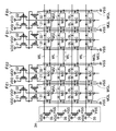
図7において、このSRAMが図10のSRAMと異なる点は、メモリセルMCが横長型であり、各ビット線対BL,/BLに対してPチャネルMOSトランジスタ21,22が追加されており、メモリセル電源配線MVLが各列に対応して設けられてビット線対BL,/BLと同じ方向に延在し、各メモリセル列に対応して図1のプログラム回路2(図示せず)が設けられている点である。
【0067】
PチャネルMOSトランジスタ21は、電源電位VDDのラインとPチャネルMOSトランジスタ31,32のソースとの間に接続される。PチャネルMOSトランジスタ22は、図1のPチャネルMOSトランジスタ1と同様に比較的高い抵抗値(10KΩ程度以上)を有し、電源電位VDD′のラインとメモリセル電源配線MVLとの間に接続される。それぞれn列(ただし、nは自然数である)に対応して設けられたn個のプログラム回路2の出力信号φE1〜φEnの各々は、対応の列のPチャネルMOSトランジスタ21,22のゲートに入力される。
【0068】
横長型メモリセルMCは、図8(a)に示すように、図11(a)(b)で示した縦長型メモリセルMCと同様に、負荷トランジスタ(PチャネルMOSトランジスタ)41,42、ドライバトランジスタ(NチャネルMOSトランジスタ)43,44およびアクセストランジスタ(NチャネルMOSトランジスタ)45,46を含む。横長型メモリセルMCと縦長型メモリセルMCでは、トランジスタ41〜46などのレイアウトが異なる。
【0069】
すなわち、横長型メモリセルMCは、図8(b)に示すように、1つのN型ウェルNWとその両側に配置されたP型ウェルPW,PWの表面に形成される。まず、N型ウェルNWから一方のP型ウェルPWにわたって図中X方向に延在するゲート電極GE1と、N型ウェルNWから他方のP型ウェルPWにわたって図中X方向に延在するゲート電極GE2と、一方のP型ウェルPW上に図中X方向に延在するゲート電極GE3と、他方のP型ウェルPW上に図中X方向に延在するゲート電極GE4とがポリシリコン層によって形成される。
【0070】
次いで、一方のP型ウェルPWにおいてゲート電極GE1,GE3を横切るようにしてN型活性層NA1が形成され、他方のP型ウェルPWにおいてゲート電極GE2,GE4を横切るようにしてN型活性層NA2が形成され、N型ウェルNWにおいてそれぞれゲート電極GE1,GE2を横切るようにしてP型活性層PA1,PA2が形成される。
【0071】
ゲート電極GE1とP型活性層PA1、ゲート電極GE2とP型活性層PA2は、それぞれPチャネルMOSトランジスタ41,42を構成する。ゲート電極GE1とN型活性層NA1、ゲート電極GE3とN型活性層NA1は、それぞれNチャネルMOSトランジスタ43,45を構成する。ゲート電極GE2とN型活性層NA2、ゲート電極GE4とN型活性層NA2は、それぞれNチャネルMOSトランジスタ44,46を構成する。
【0072】
次に、N型活性層NA1の中央部、P型活性層PA1の一方端部およびゲート電極GE2の一方端部にわたってローカル配線LL1が形成されるとともに、N型活性層NA2の中央部、P型活性層PA1の一方端部およびゲート電極GE1の一方端部にわたってローカル配線LL2が形成される。図8(b)において、ローカル配線LL1と活性層NA1,PA1とが重なっている部分は導通している。ローカル配線LL2と活性層NA2,PA2とが重なっている部分は導通している。ゲート電極GE2とローカル配線LL1、ゲート電極GE1とローカル配線LL2は、それぞれコンタクトホールCH,CHを介して互いに接続される。
【0073】
次に図8(c)に示すように、図中X方向に延在する複数のメタル配線MLが第1アルミ配線層によって形成され、さらにその上方に、図中Y方向に延在するメモリセル接地配線MGL、ビット線BL、メモリセル電源配線MVL、ビット線/BLおよびメモリセル接地線MGLが第2アルミ配線層によって形成される。複数のメタル配線MLのうちメモリセルMCの中央部を横切るメタル配線は、ワード線WLとなる。
【0074】
P型活性層PA1の一方端部(PチャネルMOSトランジスタ41のソース)は、コンタクトホールCH、メタル配線MLおよびビアホールVHを介してメモリセル電源配線MVLに接続される。P型活性層PA2の一方端部(PチャネルMOSトランジスタ42のソース)は、コンタクトホールCH、メタル配線MLおよびビアホールVHを介してメモリセル電源配線MVLに接続される。
【0075】
N型活性層NA1の一方端部(NチャネルMOSトランジスタ43のソース)は、コンタクトホールCH、メタル配線MLおよびビアホールVHを介してメモリセル接地配線MGLに接続される。N型活性層NA2の一方端部(NチャネルMOSトランジスタ44のソース)は、コンタクトホールCH、メタル配線MLおよびビアホールVHを介してメモリセル接地配線MGLに接続される。
【0076】
N型活性層NA1の他方端部(NチャネルMOSトランジスタ45のドレイン)は、コンタクトホールCH、メタル配線MLおよびビアホールVHを介してビット線BLに接続される。N型活性層NA2の他方端部(NチャネルMOSトランジスタ46のドレイン)は、コンタクトホールCH、メタル配線MLおよびビアホールVHを介してビット線/BLに接続される。ゲート電極GE3,GE4は、それぞれコンタクトホールCHを介してワード線WLに接続される。
【0077】
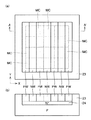
メモリセルMCの基板は、図9に示すように、トリプルウェル構造にされている。すなわち、P型シリコン基板23の表面にN+型埋込層24が形成され、さらにその表面に複数(図では4つ)のP型ウェルPWが形成され、4つのP型ウェルPWの間にそれぞれ3つのN型ウェルNWが形成される。各メモリセルMCは、N型ウェルNWとその両側に隣接するP型ウェルPWの表面に形成される。P型ウェルPWは、図中X方向に隣接する2つのメモリセルMCで共用される。図9では、4行3列に配置された12個のメモリセルMCが示されている。
【0078】
次に、このSRAMの使用法について説明する。まず、各メモリセルMCが正常か否かをテストし、不良なメモリセルMCを含むメモリセル列をスペアのメモリセル列と置換するとともに、不良なメモリセルMCを含むメモリセル列に対応するプログラム回路2のヒューズ3をブローする。
【0079】
ヒューズ3がブローされていないメモリセル列では、プログラム回路2の出力信号(たとえばφE1〜φEn−1)が「L」レベルになってPチャネルMOSトランジスタ21,22が導通する。これにより、電源電位VDDのラインからPチャネルMOSトランジスタ21,31,32を介してビット線BL,/BLに電源電位VDDが与えられるとともに、電源電位VDD′のラインからPチャネルMOSトランジスタ22を介してメモリセル電源配線MVLに電源電位VDD′が与えられ、各メモリセル列が正常に動作する。
【0080】
ヒューズ3がブローされたメモリセル列では、プログラム回路2の出力信号(この場合はφEn)が「H」レベルになってPチャネルMOSトランジスタ21,22が非導通になる。これにより、その列のビット線BL,/BLおよびメモリセル電源配線MVLはフローティング状態にされ、その列のメモリセルMCに(1)〜(9)のショートが発生している場合でもショート部分に電流は流れない。したがって、このSRAMでは、1つのヒューズ3をブローするだけで、(1)〜(9)のショートによって発生するリーク電流をなくすことができ、スタンバイ電流の低減化を図ることができる。
【0081】
今回開示された実施の形態はすべての点で例示であって制限的なものではないと考えられるべきである。本発明の範囲は上記した説明ではなくて特許請求の範囲によって示され、特許請求の範囲と均等の意味および範囲内でのすべての変更が含まれることが意図される。
【0082】
【発明の効果】
以上のように、この発明に係るスタティック型半導体記憶装置では、各ワード線に対応して設けられて対応のワード線と基準電位のラインとの間に接続され、対応のワード線が選択されていない場合に導通して対応の各メモリセルを非活性状態にするための第1のスイッチング素子と、各行または列に対応して設けられ、その一方端が対応の行または列の各メモリセルの電源ノードに接続された電源配線と、各電源配線に対応して設けられて対応の電源配線の他方端と電源電位のラインとの間に接続され、第1のスイッチング素子の導通抵抗値よりも大きな予め定められた導通抵抗値を有する第2のスイッチング素子と、各行または列に対応して設けられ、対応の行または列が不良である場合にブローされるヒューズを含み、そのヒューズがブローされたことに応じて第2のスイッチング素子を非導通にするプログラム回路とが設けられる。したがって、不良な行または列に対応するプログラム回路のヒューズを切断することにより、第2のスイッチング素子を非導通にしてその行または列の電源配線をフローティング状態にすることができる。よって、メモリセルのショート部分に電流がリークしたり、電源配線と信号線の間に電流が流れるのを防止することができ、スタンバイ電流の低減化を図ることができる。また、第2のスイッチング素子が第1のスイッチング素子の導通抵抗値よりも大きな所定の導通抵抗値を有するので、電源配線がワード線などとショートしていることを容易に検出することができ、その電源配線をフローティング状態にすることによりスタンバイ電流の低減化を図ることができる。また、第2のスイッチング素子が比較的大きな所定の導通抵抗値を有しているので、ラッチアップ現象が発生した場合でもリーク電流を抑制することができる。
【0083】
好ましくは、電源配線およびプログラム回路は各列に対応して設けられ、スタティック型半導体記憶装置は、さらに、各ビット線に対応して設けられ、その一方電極が対応のビット線に接続されたビット線負荷素子と、各列に対応して設けられて対応の列の各ビット線負荷素子の他方電極と電源電位のラインとの間に接続された第3のスイッチング素子とを備え、プログラム回路は、ヒューズがブローされたことに応じて第2のスイッチング素子とともに第3のスイッチング素子も非導通にする。この場合は、不良な列に対応する1つのヒューズを切断することにより、その列の電源配線およびビット線対から流出する電流を遮断することができる。
【0084】
また好ましくは、プログラム回路は、第1のノードと第1の電位のラインとの間に接続され、リセット信号が第1のレベルから第2のレベルに変化したことに応じて導通し、第1のノードの電位を第1の電位にリセットするための第4のスイッチング素子と、第1のノードと第2の電位のラインとの間にヒューズと直列接続され、リセット信号が第2のレベルから第1のレベルに変化したことに応じて導通し、ヒューズがブローされていない場合に第1のノードを第2の電位にするための第5のスイッチング素子と、リセット信号が第2のレベルから第1のレベルに変化してから予め定められた時間だけ経過したことに応じて第1のノードの電位をラッチし、ラッチした電位が第1の電位の場合に第2のスイッチング素子を非導通にするためのラッチ回路とを含む。この場合は、ヒューズが不十分にブローされている場合でも、ヒューズが十分にブローされている場合と同じ結果を得ることができる。
【0085】
また好ましくは、さらに、第1の導電形式の半導体基板と、半導体基板の表面に形成された第2の導電形式の半導体埋込層と、半導体埋込層の表面に形成された第1の導電形式の複数の第1のウェルと、半導体埋込層の表面に複数の第1のウェルの間にそれぞれ形成された第2の導電形式の複数の第2のウェルとが設けられ、複数のメモリセルは、複数の第1のウェルおよび複数の第2のウェルの表面に形成される。この場合は、半導体基板で発生した電子−ホール対が半導体埋込層に吸収されるので、ソフトエラーの発生を抑制することができる。
【0086】
また好ましくは、第2のスイッチング素子は、予め定められた導通抵抗値を有するトランジスタを含む。この場合は、第2のスイッチング素子を容易に構成できる。
【0087】
また好ましくは、第2のスイッチング素子は、予め定められた導通抵抗値を有する抵抗素子と、電源配線の他方端と電源電位のラインとの間に抵抗素子と直列接続されたトランジスタとを含む。この場合は、第2のスイッチング素子の導通抵抗値を容易かつ正確に設定できる。
【図面の簡単な説明】
【図1】 この発明の実施の形態1によるSRAMの要部を示す回路ブロック図である。
【図2】 図1に示したプログラム回路の動作を示すタイムチャートである。
【図3】 図1で説明したSRAMをより詳細に示す回路ブロック図である。
【図4】 図3に示したSRAMの効果を説明するための回路図である。
【図5】 図1に示したSRAMの効果を説明するための回路ブロック図である。
【図6】 実施の形態1の変更例を示す回路ブロック図である。
【図7】 この発明の実施の形態2によるSRAMの要部を示す回路ブロック図である。
【図8】 図7に示したメモリセルの構成およびレイアウトを示す図である。
【図9】 図8に示したメモリセルの基板を示す図である。
【図10】 従来のSRAMの全体構成を示す回路ブロック図である。
【図11】 図10に示したメモリセルの構成およびレイアウトを示す図である。
【図12】 図11に示したメモリセルの基板を示す図である。
【図13】 従来の他のSRAMの要部を示す回路ブロック図である。
【図14】 図13に示したSRAMをより詳細に示す回路ブロック図である。
【図15】 図14に示したSRAMの問題点を説明するための図である。
【図16】 従来のさらに他のSRAMの要部を示す回路ブロック図である。
【図17】 従来のさらに他のSRAMの要部を示す回路ブロック図である。
【図18】 従来のさらに他のSRAMの要部を示す回路ブロック図である。
【符号の説明】
1,4,13,21,22,41,42,64 PチャネルMOSトランジスタ、2,60 プログラム回路、3,50,61,70 ヒューズ、5,35,43〜46,62,63 NチャネルMOSトランジスタ、6 トランスファゲート、7〜9,67 インバータ、11,12 異物、14,51,52 抵抗素子、23,47 P型シリコン基板、24,48 N+型埋込層、31,32ビット線負荷、33 列選択ゲート、34 行デコーダ、36 制御回路、37 列デコーダ、38 書込回路、39 読出回路、53 PNPバイポーラトランジスタ、54 NPNバイポーラトランジスタ、66 電源電位供給回路、PW P型ウェル、NW N型ウェル、PA P型活性層、NA N型活性層、GE ゲート電極、MC メモリセル、WL ワード線、BL,/BL ビット線対、CSL 列選択線、IO,/IO データ入出力線対、MVL メモリセル電源配線、MGL メモリセル接地配線、WVL ウェル電源配線、WGL ウェル接地配線、CH コンタクトホール、VH ビアホール、LL ローカル配線、ML メタル配線。[0001]
BACKGROUND OF THE INVENTION
The present invention relates to a static semiconductor memory device, and more particularly to a static semiconductor memory device adopting a redundancy system in which a defective row or column is replaced with a spare row or column.
[0002]
[Prior art]
FIG. 10 is a circuit block diagram showing a configuration of a conventional static random access memory (hereinafter referred to as SRAM).
[0003]
In FIG. 10, this SRAM includes a plurality of memory cells MC arranged in a plurality of rows and a plurality of columns (4 rows and 4 columns in the figure), word lines WL provided corresponding to each row, and corresponding to each column. A provided bit line pair BL, / BL is provided.
[0004]
The SRAM is provided corresponding to each bit line pair BL, / BL,
[0005]
[0006]
The SRAM further includes a
[0007]
Write
[0008]
Next, the operation of the SRAM shown in FIG. 10 will be described. During the write operation, the word line WL in the row corresponding to the row address signal is raised to the “H” level of the selection level by the
[0009]
Write
[0010]
In the read operation, the column selection line CSL of the column corresponding to the column address signal is raised to the “H” level of the selection level by the
[0011]
FIG. 11A is a circuit diagram showing a configuration of the memory cell MC. In FIG. 11A, memory cell MC includes load transistors (P channel MOS transistors) 41 and 42, driver transistors (N channel MOS transistors) 43 and 44, and access transistors (N channel MOS transistors) 45 and 46. . P-
[0012]
During the write operation, one of bit lines BL, / BL is set to “H” level and the other is set to “L” level according to write data DI. Next, word line WL is set to the “H” level of the selection level, N
[0013]
In the read operation, each of bit lines BL and / BL is charged to “H” level by
[0014]
FIG. 11B shows a layout of the memory cell MC. Two gate electrodes GE1 and GE2 extending in the Y direction in the drawing are formed in parallel on the surface of the silicon substrate, and a word line WL extending in the X direction in the drawing is formed. Gate electrodes GE1, GE2 and word line WL are formed of a polysilicon layer. P-type active layers PA1 and PA2 are formed from one side to the other side of one end of the gate electrodes GE1 and GE2, respectively. An N-type active layer NA1 is formed from one side of the other end of the gate electrode GE1 to the other side and from one side of the one end of the word line WL to the other side. An N-type active layer NA2 is formed from one side to the other side of the other end of the gate electrode GE2 and from one side to the other side of the other end of the word line WL.
[0015]
The P-type active layer PA1 and the gate electrode GE1, and the P-type active layer PA2 and the gate electrode GE2 constitute P-
[0016]
Next, a plurality of local wirings LL are formed. In FIG. 11B, the local wiring LL and the active layer are conductive at the portion where the local wiring LL and the active layer overlap. One end portions of active layers PA1, PA2 (sources of P
[0017]
The other end of P-type active layer PA1 (the drain of P-channel MOS transistor 41) is connected to the central portion of N-type active layer NA1 (the drains of N-
[0018]
Further, bit lines BL, / BL and memory cell ground lines MGL, MGL extending in the Y direction in the figure are formed in parallel by the first aluminum wiring layer. One end portions of N-type active layers NA1, NA2 (sources of N-
[0019]
The substrate of the memory cell MC has a triple well structure as shown in FIG. That is, N on the surface of the P-type silicon substrate 47.+A type buried
[0020]
In such an SRAM, foreign matter adheres to the memory cell MC during manufacturing, and (1) a short circuit between the storage nodes N1 and N2, (2) a short circuit between the storage node N1 or N2 and the memory cell power supply wiring MVL, (3) Short circuit between storage node N1 or N2 and memory cell ground wiring MGL, (4) Short circuit between storage node N1 or N2 and word line WL, (5) Between storage node N1 or N2 and bit line BL or / BL (6) A short circuit between the bit line BL or / BL and the word line WL, (7) A short circuit between the word line WL and the memory cell power supply wiring MVL, (8) A bit line BL or / BL and the memory cell ground wiring A short circuit between the MGLs and (9) a short circuit between the memory cell power supply wiring MVL and the memory cell ground wiring MGL may occur. In the memory cell MC shown in FIG. 11, since the bit lines BL, / BL and the memory cell ground wirings MGL, MGL are arranged adjacent to each other in parallel, the short circuit (8) is particularly likely to occur.
[0021]
The memory cell MC in which such a short circuit occurs does not operate normally. Therefore, in the SRAM, a spare row or column for replacing the row or column including the defective memory cell MC and a program circuit for programming the address of the defective row or column are provided, and the defective row or column is provided. When the address is input, a redundancy method is adopted in which a defective product is relieved by selecting a spare row or column instead of a defective row or column.
[0022]
However, if a defective row or column is simply replaced with a spare row or column, leakage current continues to flow through the shorted portion, and the standby current exceeds the standard value. Therefore, various methods have been proposed to reduce the standby current.
[0023]
In the method of FIG. 13, a
[0024]
[Problems to be solved by the invention]
However, this method has a problem that the standby current is not sufficiently reduced when the blow of the
[0025]
FIG. 14 is a diagram showing the SRAM to which the method shown in FIG. 13 is applied in more detail. In FIG. 14, in this SRAM, a well power supply wiring WVL and a well ground wiring WGL are provided for each of a plurality of columns (64 columns in the figure). Each well power supply wiring WVL receives power supply potential VDD and is connected to each N-type well NW in FIG. 12 through contact hole CH. Each well ground wiring WGL receives a ground potential VSS and is connected to each P-type well PW in FIG. 12 through a contact hole CH. As a result, it is possible to prevent current from flowing from the active layer PA or NA of the MOS transistor to the well NW or PW. Each memory cell power supply wiring MVL is connected to a line of power supply potential VDD ′ (VDD ′ = VDD) through a
[0026]
However, this SRAM has a problem that it is vulnerable to latch-up. That is, as shown in FIGS. 15A and 15B, the N-type well NW and the P-type well PW constitute
[0027]
If for some reason a latch-up trigger occurs in the N-type well NW or P-type well PW and the base-emitter voltages of the
[0028]
In the method of FIG. 16, a
[0029]
When
[0030]
However, in this method, when the blow of the
[0031]
Further, since the memory cell power supply wiring MVL in the defective row is fixed to the ground potential VSS, the signal wiring of the signal that becomes “H” level during standby and the memory cell power supply wiring MVL set to the ground potential VSS are short-circuited. In this case, a standby current failure occurs.
[0032]
In the method of FIG. 17, a
[0033]
However, this method also has a problem that the standby current is not sufficiently reduced when the blow of the
[0034]
In the method of FIG. 18, the gates of P-
[0035]
However, in this method, each bit line pair BL, / BL is brought into a floating state during standby, so that each bit line pair BL, / BL is charged to "H" level when the standby mode is shifted to the read mode. There is a problem in that the time for reading is required and the reading speed is delayed.
[0036]
Further, in the method shown in FIGS. 13 to 18, when some of the shorts of (1) to (9) are short, the standby current can be reduced, but there is another short. Had a problem that the standby current could not be reduced. For example, in the method of FIG. 13, the standby current can be reduced when there is a short circuit of (1) to (4), (7), and (9), but when there is a short circuit of (6), the “H” level bit Current leaks from the lines BL, / BL to the “L” level word line WL, and the standby current cannot be reduced. In the method of FIG. 17, the standby current can be reduced when there is a short circuit of (5), (6), and (8), but when there is a short circuit of (1) to (4), (7), and (9). Current leaks from the memory cell power line MVL to the line of the ground potential VSS, and the standby current cannot be reduced.
[0037]
Therefore, a main object of the present invention is to provide a static semiconductor memory device having a small standby current and strong against latch-up.
[0038]
[Means for Solving the Problems]
A static semiconductor memory device according to the present invention includes a plurality of memory cells arranged in a plurality of rows and a plurality of columns, a word line provided corresponding to each row, and a bit line pair provided corresponding to each column. A static semiconductor memory device adopting a redundancy system that replaces a defective row or column with a spare row or column, and is provided corresponding to each word line and corresponding word line and reference potential line And a first switching element that is rendered conductive when the corresponding word line is not selected and deactivates each corresponding memory cell, and is provided corresponding to each row or column A power supply line having one end connected to the power supply node of each memory cell in the corresponding row or column, and a line between the other end of the corresponding power supply line and the power supply potential line provided corresponding to each power supply line Connected to the second The second switching element having a predetermined conduction resistance value larger than the conduction resistance value of the switching element is provided corresponding to each row or column, and blown when the corresponding row or column is defective A program circuit that includes a fuse and makes the second switching element non-conductive in response to the blow of the fuse.
[0039]
Preferably, the power supply wiring and the program circuit are provided corresponding to each column, and the static semiconductor memory device is further provided corresponding to each bit line, the bit of which one electrode is connected to the corresponding bit line A program circuit comprising: a line load element; and a third switching element provided corresponding to each column and connected between the other electrode of each bit line load element in the corresponding column and a power supply potential line. In response to the blow of the fuse, the third switching element is made nonconductive as well as the second switching element.
[0040]
Preferably, the program circuit is connected between the first node and the first potential line, and is turned on in response to the reset signal changing from the first level to the second level. A fourth switching element for resetting the potential of the node to the first potential and a fuse connected in series between the first node and the second potential line, and the reset signal from the second level A fifth switching element that conducts in response to the change to the first level and sets the first node to the second potential when the fuse is not blown, and the reset signal from the second level. The potential of the first node is latched in response to the elapse of a predetermined time after changing to the first level, and the second switching element is made non-conductive when the latched potential is the first potential To make And a latch circuit.
[0041]
More preferably, the semiconductor substrate of the first conductivity type, the second conductivity type semiconductor buried layer formed on the surface of the semiconductor substrate, and the first conductivity type formed on the surface of the semiconductor buried layer are further provided. A plurality of first wells of a type, and a plurality of second wells of a second conductivity type respectively formed between the plurality of first wells on the surface of the semiconductor buried layer, and a plurality of memories The cells are formed on the surfaces of the plurality of first wells and the plurality of second wells.
[0042]
Preferably, the second switching element includes a transistor having a predetermined conduction resistance value.
[0043]
Preferably, the second switching element includes a resistance element having a predetermined conduction resistance value, and a transistor connected in series with the resistance element between the other end of the power supply wiring and the power supply potential line..
[0044]
DETAILED DESCRIPTION OF THE INVENTION
[Embodiment 1]
FIG. 1 is a circuit block diagram showing a main part of the SRAM according to the first embodiment of the present invention, which is compared with FIG.
[0045]
In FIG. 1, the SRAM is different from the SRAM of FIG. 13 in that the
[0046]
Program circuit 2 includes a fuse 3, a P channel MOS transistor 4, an N
[0047]
[0048]
FIG. 2 is a time chart showing the operation of the program circuit 2 shown in FIG. In FIG. 2, in the initial state, signals RST and RSTD are both at "L" level, P channel MOS transistor 4 is turned on, and N
[0049]
Next, when signal RSTD is raised from “L” level to “H” level at time t2,
[0050]
At this time, if fuse 3 is not blown, power supply potential VDD is applied to node N4 via fuse 3 and P-channel MOS transistor 4, and node N4 is raised from "L" level to "H" level. , Signal φE falls from “H” level to “L” level. Further, when the fuse 3 is sufficiently blown, the node N4 remains unchanged at the “L” level, and the signal φE remains unchanged at the “H” level. When the fuse 3 is blown insufficiently, the insufficiently blown fuse 3 has a high resistance value, so that the potential of the node N4 gradually rises and the potential of the node N4 is reduced by the inverter 8. It takes a long time to exceed the threshold potential. Until the potential of node N4 exceeds the threshold potential of inverter 8, signal φE remains at “H” level. Next, when signal RSTD falls from “H” level to “L” level at time t 4,
[0051]
Therefore, the signal φE is at “L” level when the fuse 3 is not blown, and the signal φE is “H” when the fuse 3 is sufficiently blown and when the fuse 3 is blown insufficiently. Become a level.
[0052]
Next, a method of using this SRAM will be described. First, it is tested whether each memory cell MC is normal, a memory cell row including a defective memory cell MC is replaced with a spare memory cell row, and a program corresponding to the memory cell row including the defective memory cell MC The fuse 3 of the circuit 2 is blown.
[0053]
In the memory cell row where the fuse 3 is not blown, the output signal φE of the program circuit 2 becomes “L” level and the P-
[0054]
Further, in the memory cell row in which fuse 3 is sufficiently blown and the memory cell row in which fuse 3 is blown insufficiently, output signal φE of program circuit 2 attains an “H” level and P
[0055]
Further, the memory cell power supply wiring MVL of the defective memory cell row is set in a floating state instead of being grounded as in the SRAM of FIG. Therefore, even when a signal line that transmits a signal that goes to “H” level during standby and the memory cell power supply wiring MVL are short-circuited, no current flows between the signal line and the memory cell power supply wiring MVL. The standby current can be reduced.
[0056]
FIG. 3 is a diagram showing the configuration of this SRAM in more detail, and is a diagram contrasted with FIG. 3, the SRAM differs from the SRAM of FIG. 14 in that each
[0057]
This SRAM has a structure resistant to latch-up. That is, also in this SRAM, as described with reference to FIG. 15B, the wells NW and PW and the active layers PA and NA form a discharge circuit including the
[0058]
Further, this SRAM is configured to easily detect the short circuit of (7) and (9). That is, as shown in FIG. 5, consider the case (7) where the memory cell power supply wiring MVL and the word line WL are short-circuited by the low-resistance foreign material 11 (the
[0059]
Therefore, when the conduction resistance value of P-
[0060]
However, in this SRAM, the conduction resistance value of the P-
[0061]
Next, consider the case (9) in which the memory cell power supply wiring MVL and the memory cell ground wiring MGL are short-circuited by the
[0062]
Therefore, when the conduction resistance value of P-
[0063]
However, in this SRAM, the conduction resistance value of the P-
[0064]
In the first embodiment, the P
[0065]
[Embodiment 2]
FIG. 7 is a circuit block diagram showing a main part of the SRAM according to the second embodiment of the present invention, which is compared with FIG.
[0066]
In FIG. 7, this SRAM differs from the SRAM of FIG. 10 in that the memory cell MC is a horizontally long type, and P
[0067]
P
[0068]
As shown in FIG. 8A, the horizontally long memory cell MC includes load transistors (P-channel MOS transistors) 41 and 42, drivers, as in the vertically long memory cell MC shown in FIGS. Transistors (N channel MOS transistors) 43 and 44 and access transistors (N channel MOS transistors) 45 and 46 are included. The layout of the
[0069]
That is, the horizontally long memory cell MC is formed on the surface of one N-type well NW and P-type wells PW and PW arranged on both sides thereof, as shown in FIG. 8B. First, a gate electrode GE1 extending in the X direction from the N type well NW to one P type well PW, and a gate electrode GE2 extending from the N type well NW to the other P type well PW in the X direction in the drawing. A gate electrode GE3 extending in the X direction in the drawing on one P-type well PW and a gate electrode GE4 extending in the X direction in the drawing on the other P-type well PW are formed by a polysilicon layer. The
[0070]
Next, an N-type active layer NA1 is formed across the gate electrodes GE1 and GE3 in one P-type well PW, and an N-type active layer NA2 across the gate electrodes GE2 and GE4 in the other P-type well PW. P-type active layers PA1 and PA2 are formed in the N-type well NW so as to cross the gate electrodes GE1 and GE2, respectively.
[0071]
The gate electrode GE1 and the P-type active layer PA1, and the gate electrode GE2 and the P-type active layer PA2 constitute P-
[0072]
Next, a local wiring LL1 is formed across the central portion of the N-type active layer NA1, one end portion of the P-type active layer PA1, and one end portion of the gate electrode GE2, and the central portion of the N-type active layer NA2 A local wiring LL2 is formed across one end of the active layer PA1 and one end of the gate electrode GE1. In FIG. 8B, the portion where the local wiring LL1 and the active layers NA1 and PA1 overlap is conductive. The portion where the local wiring LL2 and the active layers NA2 and PA2 overlap is conductive. The gate electrode GE2 and the local wiring LL1, and the gate electrode GE1 and the local wiring LL2 are connected to each other through contact holes CH and CH, respectively.
[0073]
Next, as shown in FIG. 8C, a plurality of metal wirings ML extending in the X direction in the figure are formed by the first aluminum wiring layer, and further above, the memory cells extending in the Y direction in the figure Ground wiring MGL, bit line BL, memory cell power supply wiring MVL, bit line / BL and memory cell ground line MGL are formed by the second aluminum wiring layer. Of the plurality of metal wirings ML, the metal wiring crossing the central portion of the memory cell MC becomes the word line WL.
[0074]
One end portion of P-type active layer PA1 (the source of P-channel MOS transistor 41) is connected to memory cell power supply wiring MVL through contact hole CH, metal wiring ML, and via hole VH. One end portion of P-type active layer PA2 (the source of P-channel MOS transistor 42) is connected to memory cell power supply wiring MVL through contact hole CH, metal wiring ML, and via hole VH.
[0075]
One end of N-type active layer NA1 (the source of N-channel MOS transistor 43) is connected to memory cell ground wiring MGL via contact hole CH, metal wiring ML, and via hole VH. One end of N-type active layer NA2 (the source of N-channel MOS transistor 44) is connected to memory cell ground wiring MGL via contact hole CH, metal wiring ML, and via hole VH.
[0076]
The other end of N-type active layer NA1 (the drain of N-channel MOS transistor 45) is connected to bit line BL via contact hole CH, metal interconnection ML, and via hole VH. The other end of N-type active layer NA2 (the drain of N-channel MOS transistor 46) is connected to bit line / BL via contact hole CH, metal interconnection ML, and via hole VH. Gate electrodes GE3 and GE4 are each connected to word line WL through contact hole CH.
[0077]
The substrate of the memory cell MC has a triple well structure as shown in FIG. That is, N on the surface of the P-type silicon substrate 23.+A type buried
[0078]
Next, the usage of this SRAM will be described. First, it is tested whether each memory cell MC is normal, a memory cell column including a defective memory cell MC is replaced with a spare memory cell column, and a program corresponding to the memory cell column including the defective memory cell MC The fuse 3 of the circuit 2 is blown.
[0079]
In a memory cell column in which fuse 3 is not blown, the output signals (for example, φE1 to φEn-1) of program circuit 2 attain an “L” level, and P
[0080]
In the memory cell row in which the fuse 3 is blown, the output signal (in this case, φEn) of the program circuit 2 becomes “H” level, and the P-
[0081]
The embodiment disclosed this time should be considered as illustrative in all points and not restrictive. The scope of the present invention is defined by the terms of the claims, rather than the description above, and is intended to include any modifications within the scope and meaning equivalent to the terms of the claims.
[0082]
【The invention's effect】
As described above, in the static semiconductor memory device according to the present invention, a corresponding word line is selected corresponding to each word line and connected between the corresponding word line and the reference potential line. A first switching element for conducting each of the corresponding memory cells in an inactive state when there is not, and a first switching element corresponding to each row or column, one end of which is provided for each memory cell in the corresponding row or column A power supply wiring connected to the power supply node, and connected between the other end of the corresponding power supply wiring and the power supply potential line corresponding to each power supply wiring, and more than the conduction resistance value of the first switching element A second switching element having a large predetermined conduction resistance value and a fuse provided corresponding to each row or column and blown when the corresponding row or column is defective, A program circuit for the second switching element non-conductive in response to which the rows are provided. Therefore, by cutting the fuse of the program circuit corresponding to the defective row or column, the second switching element can be made non-conductive and the power supply wiring of that row or column can be brought into a floating state. Accordingly, it is possible to prevent a current from leaking to a short portion of the memory cell and a current from flowing between the power supply wiring and the signal line, and to reduce the standby current. Further, since the second switching element has a predetermined conduction resistance value larger than the conduction resistance value of the first switching element, it is possible to easily detect that the power supply wiring is short-circuited with a word line or the like, The standby current can be reduced by bringing the power supply wiring into a floating state. In addition, since the second switching element has a relatively large predetermined conduction resistance value, the leakage current can be suppressed even when the latch-up phenomenon occurs.
[0083]
Preferably, the power supply wiring and the program circuit are provided corresponding to each column, and the static semiconductor memory device is further provided corresponding to each bit line, the bit of which one electrode is connected to the corresponding bit line A program circuit comprising: a line load element; and a third switching element provided corresponding to each column and connected between the other electrode of each bit line load element in the corresponding column and a power supply potential line. In response to the blow of the fuse, the third switching element is made nonconductive as well as the second switching element. In this case, by cutting one fuse corresponding to the defective column, the current flowing out from the power supply wiring and the bit line pair in that column can be cut off.
[0084]
Preferably, the program circuit is connected between the first node and the first potential line, and is turned on in response to the reset signal changing from the first level to the second level. A fourth switching element for resetting the potential of the node to the first potential and a fuse connected in series between the first node and the second potential line, and the reset signal from the second level A fifth switching element that conducts in response to the change to the first level and sets the first node to the second potential when the fuse is not blown, and the reset signal from the second level. The potential of the first node is latched in response to the elapse of a predetermined time after changing to the first level, and the second switching element is made non-conductive when the latched potential is the first potential To make And a latch circuit. In this case, even when the fuse is blown insufficiently, the same result as when the fuse is blown sufficiently can be obtained.
[0085]
More preferably, the semiconductor substrate of the first conductivity type, the second conductivity type semiconductor buried layer formed on the surface of the semiconductor substrate, and the first conductivity type formed on the surface of the semiconductor buried layer are further provided. A plurality of first wells of a type, and a plurality of second wells of a second conductivity type respectively formed between the plurality of first wells on the surface of the semiconductor buried layer, and a plurality of memories The cells are formed on the surfaces of the plurality of first wells and the plurality of second wells. In this case, since electron-hole pairs generated in the semiconductor substrate are absorbed by the semiconductor buried layer, the occurrence of soft errors can be suppressed.
[0086]
Preferably, the second switching element includes a transistor having a predetermined conduction resistance value. In this case, the second switching element can be easily configured.
[0087]
Preferably, the second switching element includes a resistance element having a predetermined conduction resistance value, and a transistor connected in series with the resistance element between the other end of the power supply wiring and the power supply potential line. In this case, the conduction resistance value of the second switching element can be set easily and accurately..
[Brief description of the drawings]
FIG. 1 is a circuit block diagram showing a main part of an SRAM according to a first embodiment of the present invention;
FIG. 2 is a time chart showing the operation of the program circuit shown in FIG.
FIG. 3 is a circuit block diagram showing the SRAM described in FIG. 1 in more detail.
4 is a circuit diagram for explaining an effect of the SRAM shown in FIG. 3; FIG.
FIG. 5 is a circuit block diagram for explaining an effect of the SRAM shown in FIG. 1;
FIG. 6 is a circuit block diagram showing a modification of the first embodiment.
FIG. 7 is a circuit block diagram showing a main part of an SRAM according to a second embodiment of the present invention.
8 is a diagram showing the configuration and layout of the memory cell shown in FIG. 7;
9 is a diagram showing a substrate of the memory cell shown in FIG. 8. FIG.
FIG. 10 is a circuit block diagram showing an overall configuration of a conventional SRAM.
11 is a diagram showing the configuration and layout of the memory cell shown in FIG. 10;
12 is a diagram showing a substrate of the memory cell shown in FIG. 11. FIG.
FIG. 13 is a circuit block diagram showing a main part of another conventional SRAM.
FIG. 14 is a circuit block diagram showing the SRAM shown in FIG. 13 in more detail.
FIG. 15 is a diagram for explaining a problem of the SRAM shown in FIG. 14;
FIG. 16 is a circuit block diagram showing a main part of still another conventional SRAM.
FIG. 17 is a circuit block diagram showing a main part of still another conventional SRAM.
FIG. 18 is a circuit block diagram showing a main part of still another conventional SRAM.
[Explanation of symbols]
1, 4, 13, 21, 22, 41, 42, 64 P-channel MOS transistor, 2,60 program circuit, 3, 50, 61, 70 fuse, 5, 35, 43 to 46, 62, 63 N-channel MOS transistor , 6 Transfer gate, 7-9, 67 Inverter, 11, 12 Foreign object, 14, 51, 52 Resistance element, 23, 47 P-type silicon substrate, 24, 48 N+Type buried layer, 31, 32 bit line load, 33 column select gate, 34 row decoder, 36 control circuit, 37 column decoder, 38 write circuit, 39 read circuit, 53 PNP bipolar transistor, 54 NPN bipolar transistor, 66 power supply Potential supply circuit, PWP type well, NW N type well, PAPP type active layer, NAN type active layer, GE gate electrode, MC memory cell, WL word line, BL / BL bit line pair, CSL column selection line , IO, / IO data input / output line pair, MVL memory cell power supply wiring, MGL memory cell ground wiring, WVL well power supply wiring, WGL well ground wiring, CH contact hole, VH via hole, LL local wiring, ML metal wiring.
Claims (6)
各ワード線に対応して設けられて対応のワード線と基準電位のラインとの間に接続され、対応のワード線が選択されていない場合に導通して対応の各メモリセルを非活性状態にするための第1のスイッチング素子、
各行または列に対応して設けられ、その一方端が対応の行または列の各メモリセルの電源ノードに接続された電源配線、
各電源配線に対応して設けられて対応の電源配線の他方端と電源電位のラインとの間に接続され、前記第1のスイッチング素子の導通抵抗値よりも大きな予め定められた導通抵抗値を有する第2のスイッチング素子、および
各行または列に対応して設けられ、対応の行または列が不良である場合にブローされるヒューズを含み、該ヒューズがブローされたことに応じて前記第2のスイッチング素子を非導通にするプログラム回路を備える、スタティック型半導体記憶装置。A plurality of memory cells arranged in a plurality of rows and a plurality of columns, a word line provided corresponding to each row, and a bit line pair provided corresponding to each column, and a defective row or column as a spare row Or a static semiconductor memory device adopting a redundancy method of replacing by a column,
Provided corresponding to each word line, connected between the corresponding word line and the reference potential line, and conducts when the corresponding word line is not selected, and deactivates each corresponding memory cell. A first switching element for
Power supply wiring provided corresponding to each row or column, one end of which is connected to the power supply node of each memory cell in the corresponding row or column,
Provided corresponding to each power supply wiring, connected between the other end of the corresponding power supply wiring and the power supply potential line, and having a predetermined conduction resistance value larger than the conduction resistance value of the first switching element. A second switching element, and a fuse provided corresponding to each row or column and blown when the corresponding row or column is defective, and the second switching element in response to the blow of the fuse A static semiconductor memory device comprising a program circuit for making a switching element nonconductive.
前記スタティック型半導体記憶装置は、
さらに、各ビット線に対応して設けられ、その一方電極が対応のビット線に接続されたビット線負荷素子、および
各列に対応して設けられて対応の列の各ビット線負荷素子の他方電極と電源電位のラインとの間に接続された第3のスイッチング素子を備え、
前記プログラム回路は、前記ヒューズがブローされたことに応じて前記第2のスイッチング素子とともに前記第3のスイッチング素子も非導通にする、請求項1に記載のスタティック型半導体記憶装置。The power supply wiring and the program circuit are provided corresponding to each column,
The static semiconductor memory device includes:
Further, a bit line load element provided corresponding to each bit line and having one electrode connected to the corresponding bit line, and the other of each bit line load element provided corresponding to each column. A third switching element connected between the electrode and the power supply potential line;
2. The static semiconductor memory device according to claim 1, wherein the program circuit makes the third switching element nonconductive as well as the second switching element in response to the fuse being blown. 3.
第1のノードと第1の電位のラインとの間に接続され、リセット信号が第1のレベルから第2のレベルに変化したことに応じて導通し、前記第1のノードの電位を前記第1の電位にリセットするための第4のスイッチング素子、
前記第1のノードと第2の電位のラインとの間に前記ヒューズと直列接続され、前記リセット信号が前記第2のレベルから前記第1のレベルに変化したことに応じて導通し、前記ヒューズがブローされていない場合に前記第1のノードを前記第2の電位にするための第5のスイッチング素子、および
前記リセット信号が前記第2のレベルから前記第1のレベルに変化してから予め定められた時間だけ経過したことに応じて前記第1のノードの電位をラッチし、ラッチした電位が前記第1の電位の場合に前記第2のスイッチング素子を非導通にするためのラッチ回路を含む、請求項1または請求項2に記載のスタティック型半導体記憶装置。The program circuit includes:
The first node is connected between the first potential line and the first potential line. The reset signal is turned on in response to the change from the first level to the second level, and the potential of the first node is set to the first level. A fourth switching element for resetting to a potential of 1;
The fuse is connected in series between the first node and a second potential line, and conducts in response to the reset signal changing from the second level to the first level, and the fuse Is not blown, a fifth switching element for setting the first node to the second potential, and the reset signal from the second level to the first level in advance A latch circuit configured to latch the potential of the first node in response to elapse of a predetermined time and to turn off the second switching element when the latched potential is the first potential; The static semiconductor memory device according to claim 1, further comprising:
前記半導体基板の表面に形成された第2の導電形式の半導体埋込層、
前記半導体埋込層の表面に形成された第1の導電形式の複数の第1のウェル、および
前記半導体埋込層の表面に前記複数の第1のウェルの間にそれぞれ形成された第2の導電形式の複数の第2のウェルを備え、
前記複数のメモリセルは、前記複数の第1のウェルおよび前記複数の第2のウェルの表面に形成されている、請求項1から請求項3のいずれかに記載のスタティック型半導体記憶装置。Furthermore, a semiconductor substrate of the first conductivity type,
A semiconductor buried layer of a second conductivity type formed on the surface of the semiconductor substrate;
A plurality of first wells of a first conductivity type formed on the surface of the semiconductor buried layer, and a second well formed on the surface of the semiconductor buried layer between the plurality of first wells, respectively. Comprising a plurality of second wells of conductive type;
4. The static semiconductor memory device according to claim 1, wherein the plurality of memory cells are formed on surfaces of the plurality of first wells and the plurality of second wells. 5.
前記予め定められた導通抵抗値を有する抵抗素子、および
前記電源配線の他方端と前記電源電位のラインとの間に前記抵抗素子と直列接続されたトランジスタを含む、請求項1から請求項4のいずれかに記載のスタティック型半導体記憶装置。 The second switching element is
5. The resistance element having the predetermined conduction resistance value, and a transistor connected in series with the resistance element between the other end of the power supply wiring and the power supply potential line. The static semiconductor memory device according to any one of the above .
Priority Applications (3)
| Application Number | Priority Date | Filing Date | Title |
|---|---|---|---|
| JP2000374261A JP4530527B2 (en) | 2000-12-08 | 2000-12-08 | Static semiconductor memory device |
| US09/846,197 US6373760B1 (en) | 2000-12-08 | 2001-05-02 | Static type semiconductor memory device adopting a redundancy system |
| DE10135559A DE10135559A1 (en) | 2000-12-08 | 2001-07-20 | Static semiconductor memory device with a redundancy system |
Applications Claiming Priority (1)
| Application Number | Priority Date | Filing Date | Title |
|---|---|---|---|
| JP2000374261A JP4530527B2 (en) | 2000-12-08 | 2000-12-08 | Static semiconductor memory device |
Related Child Applications (1)
| Application Number | Title | Priority Date | Filing Date |
|---|---|---|---|
| JP2010095259A Division JP5143179B2 (en) | 2010-04-16 | 2010-04-16 | Semiconductor memory device |
Publications (3)
| Publication Number | Publication Date |
|---|---|
| JP2002176111A JP2002176111A (en) | 2002-06-21 |
| JP2002176111A5 JP2002176111A5 (en) | 2007-11-29 |
| JP4530527B2 true JP4530527B2 (en) | 2010-08-25 |
Family
ID=18843484
Family Applications (1)
| Application Number | Title | Priority Date | Filing Date |
|---|---|---|---|
| JP2000374261A Expired - Lifetime JP4530527B2 (en) | 2000-12-08 | 2000-12-08 | Static semiconductor memory device |
Country Status (3)
| Country | Link |
|---|---|
| US (1) | US6373760B1 (en) |
| JP (1) | JP4530527B2 (en) |
| DE (1) | DE10135559A1 (en) |
Families Citing this family (11)
| Publication number | Priority date | Publication date | Assignee | Title |
|---|---|---|---|---|
| US6724649B1 (en) * | 2002-12-19 | 2004-04-20 | Intel Corporation | Memory cell leakage reduction |
| JP4388274B2 (en) | 2002-12-24 | 2009-12-24 | 株式会社ルネサステクノロジ | Semiconductor memory device |
| JP4537668B2 (en) * | 2003-05-23 | 2010-09-01 | パナソニック株式会社 | Multi-port memory cell |
| US7773442B2 (en) * | 2004-06-25 | 2010-08-10 | Cypress Semiconductor Corporation | Memory cell array latchup prevention |
| US9842629B2 (en) * | 2004-06-25 | 2017-12-12 | Cypress Semiconductor Corporation | Memory cell array latchup prevention |
| US7365432B2 (en) * | 2004-08-23 | 2008-04-29 | Taiwan Semiconductor Manufacturing Company, Ltd. | Memory cell structure |
| KR100660899B1 (en) * | 2005-12-15 | 2006-12-26 | 삼성전자주식회사 | Fuse circuit capable of eliminating leakage current path in fuse circuit |
| US7961499B2 (en) * | 2009-01-22 | 2011-06-14 | Qualcomm Incorporated | Low leakage high performance static random access memory cell using dual-technology transistors |
| JP6353668B2 (en) | 2014-03-03 | 2018-07-04 | ルネサスエレクトロニクス株式会社 | Semiconductor memory device |
| JP6506925B2 (en) * | 2014-07-30 | 2019-04-24 | ローム株式会社 | Memory circuit |
| CN108242251B (en) * | 2016-12-23 | 2019-08-16 | 联华电子股份有限公司 | Dynamic random access memory |
Family Cites Families (12)
| Publication number | Priority date | Publication date | Assignee | Title |
|---|---|---|---|---|
| JPS59155954A (en) | 1983-02-24 | 1984-09-05 | Mitsubishi Electric Corp | Semiconductor memory unit |
| JPS6432670A (en) | 1988-06-15 | 1989-02-02 | Hitachi Ltd | Semiconductor memory circuit device |
| JPH0682807B2 (en) * | 1988-09-12 | 1994-10-19 | 株式会社東芝 | Semiconductor memory |
| JPH0652542B2 (en) | 1989-07-27 | 1994-07-06 | 株式会社田村電機製作所 | Shutter mechanism of card reader |
| JP3354267B2 (en) | 1994-02-18 | 2002-12-09 | 株式会社東芝 | Semiconductor memory |
| JPH08274266A (en) * | 1995-03-29 | 1996-10-18 | Hitachi Ltd | Fuse trimming circuit and semiconductor integrated circuit equipped therewith |
| KR0157339B1 (en) | 1995-06-28 | 1998-12-01 | 김광호 | Fault cell repair circuit of semiconductor memory |
| JP3758251B2 (en) * | 1995-11-06 | 2006-03-22 | セイコーエプソン株式会社 | Semiconductor memory device |
| JP3824343B2 (en) | 1996-03-29 | 2006-09-20 | 富士通株式会社 | Semiconductor device |
| JPH1011993A (en) | 1996-06-27 | 1998-01-16 | Mitsubishi Electric Corp | Semiconductor memory device |
| JP2978467B2 (en) * | 1998-03-16 | 1999-11-15 | 株式会社日立製作所 | Method for manufacturing semiconductor integrated circuit device |
| JP3401522B2 (en) * | 1998-07-06 | 2003-04-28 | 日本電気株式会社 | Fuse circuit and redundant decoder circuit |
-
2000
- 2000-12-08 JP JP2000374261A patent/JP4530527B2/en not_active Expired - Lifetime
-
2001
- 2001-05-02 US US09/846,197 patent/US6373760B1/en not_active Expired - Lifetime
- 2001-07-20 DE DE10135559A patent/DE10135559A1/en not_active Withdrawn
Also Published As
| Publication number | Publication date |
|---|---|
| US6373760B1 (en) | 2002-04-16 |
| DE10135559A1 (en) | 2002-06-27 |
| JP2002176111A (en) | 2002-06-21 |
Similar Documents
| Publication | Publication Date | Title |
|---|---|---|
| US10242733B2 (en) | Semiconductor memory device that can stably perform writing and reading without increasing current consumption even with a low power supply voltage | |
| US6574159B2 (en) | Semiconductor memory device and testing method therefor | |
| US7336533B2 (en) | Electronic device and method for operating a memory circuit | |
| US8693271B2 (en) | Method of stressing static random access memories for pass transistor defects | |
| US7038925B1 (en) | Static semiconductor memory device having T-type bit line structure | |
| JP3258676B2 (en) | Short circuit detector circuit for memory array | |
| JPH0756759B2 (en) | Static type semiconductor memory device | |
| US20090016144A1 (en) | Semiconductor memory device | |
| US5629943A (en) | Integrated circuit memory with double bitline low special test mode control from output enable | |
| JP4530527B2 (en) | Static semiconductor memory device | |
| US8542545B2 (en) | Repairing soft failures in memory cells in SRAM arrays | |
| US20040017709A1 (en) | Active restore weak write test mode | |
| JP3895838B2 (en) | Semiconductor memory device | |
| US6741510B2 (en) | Semiconductor memory device capable of performing burn-in test at high speed | |
| US6307772B1 (en) | Static type semiconductor memory device for lower current consumption | |
| JP5143179B2 (en) | Semiconductor memory device | |
| JP2002093195A (en) | Semiconductor memory and test method therefor | |
| US6556491B2 (en) | Semiconductor storage device and method of testing the same | |
| US8526253B2 (en) | Method of screening static random access memories for pass transistor defects | |
| JP2874935B2 (en) | Semiconductor memory device | |
| KR0165500B1 (en) | Fault cell identifying circuit for static random access memory | |
| JP2008251137A (en) | Semiconductor memory device | |
| JPH04209554A (en) | Row decoder circuit for semiconductor memory |
Legal Events
| Date | Code | Title | Description |
|---|---|---|---|
| A521 | Request for written amendment filed |
Free format text: JAPANESE INTERMEDIATE CODE: A523 Effective date: 20071017 |
|
| A621 | Written request for application examination |
Free format text: JAPANESE INTERMEDIATE CODE: A621 Effective date: 20071017 |
|
| A131 | Notification of reasons for refusal |
Free format text: JAPANESE INTERMEDIATE CODE: A131 Effective date: 20100216 |
|
| A977 | Report on retrieval |
Free format text: JAPANESE INTERMEDIATE CODE: A971007 Effective date: 20100218 |
|
| A711 | Notification of change in applicant |
Free format text: JAPANESE INTERMEDIATE CODE: A712 Effective date: 20100415 |
|
| A521 | Request for written amendment filed |
Free format text: JAPANESE INTERMEDIATE CODE: A523 Effective date: 20100416 |
|
| A521 | Request for written amendment filed |
Free format text: JAPANESE INTERMEDIATE CODE: A523 Effective date: 20100423 |
|
| TRDD | Decision of grant or rejection written | ||
| A01 | Written decision to grant a patent or to grant a registration (utility model) |
Free format text: JAPANESE INTERMEDIATE CODE: A01 Effective date: 20100601 |
|
| A01 | Written decision to grant a patent or to grant a registration (utility model) |
Free format text: JAPANESE INTERMEDIATE CODE: A01 |
|
| A61 | First payment of annual fees (during grant procedure) |
Free format text: JAPANESE INTERMEDIATE CODE: A61 Effective date: 20100608 |
|
| R150 | Certificate of patent or registration of utility model |
Ref document number: 4530527 Country of ref document: JP Free format text: JAPANESE INTERMEDIATE CODE: R150 Free format text: JAPANESE INTERMEDIATE CODE: R150 |
|
| FPAY | Renewal fee payment (event date is renewal date of database) |
Free format text: PAYMENT UNTIL: 20130618 Year of fee payment: 3 |
|
| FPAY | Renewal fee payment (event date is renewal date of database) |
Free format text: PAYMENT UNTIL: 20130618 Year of fee payment: 3 |
|
| FPAY | Renewal fee payment (event date is renewal date of database) |
Free format text: PAYMENT UNTIL: 20140618 Year of fee payment: 4 |
|
| S531 | Written request for registration of change of domicile |
Free format text: JAPANESE INTERMEDIATE CODE: R313531 |
|
| R350 | Written notification of registration of transfer |
Free format text: JAPANESE INTERMEDIATE CODE: R350 |
|
| EXPY | Cancellation because of completion of term |