JP4510176B2 - Method for improving effective signal in radio receiving unit - Google Patents
Method for improving effective signal in radio receiving unit Download PDFInfo
- Publication number
- JP4510176B2 JP4510176B2 JP18594599A JP18594599A JP4510176B2 JP 4510176 B2 JP4510176 B2 JP 4510176B2 JP 18594599 A JP18594599 A JP 18594599A JP 18594599 A JP18594599 A JP 18594599A JP 4510176 B2 JP4510176 B2 JP 4510176B2
- Authority
- JP
- Japan
- Prior art keywords
- signal
- amplifier
- rssi
- output voltage
- detection unit
- Prior art date
- Legal status (The legal status is an assumption and is not a legal conclusion. Google has not performed a legal analysis and makes no representation as to the accuracy of the status listed.)
- Expired - Fee Related
Links
Images


Classifications
-
- H—ELECTRICITY
- H04—ELECTRIC COMMUNICATION TECHNIQUE
- H04B—TRANSMISSION
- H04B1/00—Details of transmission systems, not covered by a single one of groups H04B3/00 - H04B13/00; Details of transmission systems not characterised by the medium used for transmission
- H04B1/06—Receivers
- H04B1/10—Means associated with receiver for limiting or suppressing noise or interference
- H04B1/109—Means associated with receiver for limiting or suppressing noise or interference by improving strong signal performance of the receiver when strong unwanted signals are present at the receiver input
-
- H—ELECTRICITY
- H03—ELECTRONIC CIRCUITRY
- H03G—CONTROL OF AMPLIFICATION
- H03G3/00—Gain control in amplifiers or frequency changers
- H03G3/20—Automatic control
- H03G3/30—Automatic control in amplifiers having semiconductor devices
- H03G3/3052—Automatic control in amplifiers having semiconductor devices in bandpass amplifiers (H.F. or I.F.) or in frequency-changers used in a (super)heterodyne receiver
- H03G3/3078—Circuits generating control signals for digitally modulated signals
Landscapes
- Engineering & Computer Science (AREA)
- Computer Networks & Wireless Communication (AREA)
- Signal Processing (AREA)
- Noise Elimination (AREA)
- Control Of Amplification And Gain Control (AREA)
- Amplifiers (AREA)
- Circuits Of Receivers In General (AREA)
Description
【0001】
【発明の属する技術分野】
本発明は、チャネルフィルタと、スイッチと、制御ユニットと、信号強度検知ユニットとを有する無線受信ユニットにおける有効信号を改善する方法から出発する。
【0002】
【従来の技術】
信号強度検知ユニットを使用して、入力信号とその後で得られる有効信号との比がどれだけの大きさか検知することが公知である。ここでの欠点は、共に増幅されるノイズ成分が信号強度検知ユニットの出力信号にエラーを生じさせるだけでなく、有効信号の品質も損なうことである。
【0003】
【発明が解決しようとする課題】
本発明の課題は、無線受信ユニットにおける有効信号改善のための方法を提供することである。
【0004】
【課題を解決するための手段】
この課題は本発明により、制御ユニットは、スイッチが第1の信号をチャネルフィルタの上流で、第2の信号をチャネルフィルタの下流で交互に信号強度検知ユニットに供給するように制御し、
信号強度検知ユニットの出力信号を制御ユニットに供給し、
該出力信号に依存して増幅器を制御するように構成して解決される。
【0005】
有利な改善実施例は従属請求項に記載されている。
【0006】
【発明の実施の形態】
出力信号は、改善すべき有効信号と直接的関係にある。出力信号が改善されれば、有効信号も改善される。出力信号が悪化すれば、有効信号も悪化する。
【0007】
それぞれ第1と第2の信号を信号検知増幅ユニットと、制御ユニットにより行われる比較器とに供給することにより、本発明の方法の適用によって改善された有効信号が得られるように増幅器が制御される。
【0008】
本発明の方法はさらに、第1の信号が有効信号成分とノイズ信号成分を含んでおり、ノイズ信号成分がチャネルフィルタにより取り出しろ波されることを特徴とする。
【0009】
ノイズ信号をチャネルフィルタにより除去することにより、ノイズ信号を伴う、または伴わない信号強度を評価することができる。
【0010】
さらに本発明の方法は、第1の増幅器により第1の信号をチャネルフィルタの上流で増幅し、第2の増幅器で第2の信号をチャネルフィルタの下流で増幅することを特徴とする。
【0011】
それぞれの信号を複数の増幅器により増幅することにより、2つの検知信号がどのように消失するかに依存して最適化を実行することができる。最適化はこの場合、十分に自動化して制御ユニットにより行うことができる。
【0012】
本発明の方法はさらに、増幅率調整が、有効信号Nとノイズ信号SおよびノイズRとの比N/(S+R)ができるだけ大きくなるように最適化されることを特徴とする。
【0013】
通常は第1の増幅器において大きな増幅率により動作され、これにより受信器ノイズが小さく保たれる。しかし本発明の方法により、第1の増幅器の増幅率が大きく、かつ強いノイズ信号が存在し、結果として小さな比N/(S+R)しか達成できないことを検出できる。この場合、出力信号の改善は、第1の増幅器の増幅率を低減し、第2の増幅器の増幅率を増大することにより得られる。
【0014】
本発明の方法はさらに、制御ユニットにより有効信号がノイズ信号よりも大きいことが検出されるときに、第1の増幅器で最大増幅率を調整し、第2の増幅器で比較的に小さな増幅率を調整することを特徴とする。
【0015】
さらに本発明は、第1の増幅器の増幅率が最小であるときに強いノイズが存在し、出力信号の比N/(S+R)が小さい場合には、周波数領域が変更されることを特徴とする。
【0016】
第1の増幅器の増幅率が小さくても、相変わらず出力信号の質が悪いときには、チャネルが変更され、有効信号をノイズと比較して増大させることにより出力信号が改善される。
【0017】
種々の信号を信号強度検知ユニットに供給するスイッチの代わりに、2つの信号強度検知ユニットを使用し、これらが連続的に2つの信号を制御ユニットに供給することも可能である。
【0018】
【実施例】
本発明を以下、図面に基づいて詳細に説明する。
【0019】
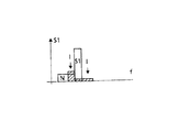
図1は、本発明の方法に対するブロック回路図を示す。入力信号ESは第1のバンドフィルタBF1,ミキサM、第1の制御可能な増幅器RV1,第2のバンドフィルタBF2を介して第2の制御可能な増幅器RV2に達する。この第2の増幅器の出力側に有効信号NSが発生する。有効信号NSは次にA/D変換器に供給される。第1のバンドフィルタBF1とミキサMとの間には、第3の制御可能な増幅器RV3を配置することもできる。この第3の増幅器は必ずしも必要ではないから、ここには破線で示されている。第3の制御可能な増幅器RV3は調整改善部として用いる。制御ユニットSEはメモリMを有している。メモリも破線で示されている。なぜならメモリは制御ユニットSEの外側に存在することもできるからである。制御ユニットSEはさらに第1の制御可能な増幅器RV1,PLL回路、スイッチS、第2の制御可能な増幅器RV2および信号強度検知ユニットRSSIと接続されている。PLL回路はさらにミキサと接続されている。第3の制御可能な増幅器RV3を使用する場合には、この増幅器も制御ユニットと接続される。スイッチSは、第1の切替位置において第1の信号S1を、第2のバンドフィルタBF2の上流で信号強度検知ユニットRSSIに供給し、第2の切替位置において第2の信号S2を、第2のバンドフィルタBF2の下流で信号強度検知ユニットRSSIに供給する。
【0020】
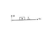
入力信号ESの供給される第1のバンドフィルタBF1には、概略的曲線が示されている。この曲線は902〜928MHzの帯域幅を示す。この帯域幅は複数の受信チャネルを含む。有効信号はこの帯域幅中にNにより、ノイズ信号はSにより示されている。ろ波された入力信号ESは次にミキサMに供給される。ミキサMは、この信号をPLL回路からの信号と混合し、混合した信号を第1の制御可能な増幅器VR1を介して第2のバンドフィルタBF2にさらに供給する。第2のバンドフィルタBF2はチャネル選択を行う。チャネル選択に用いるチャネルフィルタはここではバンドフィルタとして構成されている。スイッチSは制御ユニットSEにより制御され、まず第1の切替位置1に切り替えられる。この位置では、信号強度検知ユニットRSSIに、第1の信号S1が第2のバンドフィルタBFの上流で供給される。次に第2の切替位置2に切り替えられ、この位置では第2の信号S2が第2のバンドフィルタBF2の下流で信号強度検知ユニットRSSIに供給される。信号強度検知ユニットRSSIの出力信号ASは制御ユニットSEにも供給される。出力信号ASは電圧値であるから、以下、出力電圧の概念を使用する。制御線路ST1,ST2,および場合によりST3を介して、制御ユニットは制御可能な増幅器RV1〜RV3を調整することができ、また相応の増幅率を識別する。
【0021】
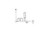
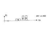
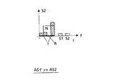
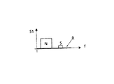
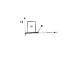
図1の機能を、図2から図23の線図に基づいて説明する。図2から図5は、信号強度測定の基本を示す。図2は、入力信号ESのスペクトルを入力周波数finに依存して示す。バンドフィルタBF1は、ISMバンド(Industrial Scientific Medical)の帯域幅を900MHzから930MHzの間に制限する。この帯域幅には有効信号Mとノイズ信号Sが存在する。図3は、有効信号Nとノイズ信号Sの第1のスペクトルS1を示す。ノイズ信号Sは有効信号Nより大きい。図4は、有効信号Nとこれより小さいノイズ信号SのスペクトルS2を示す。図5には、出力電圧ASが入力信号ESの信号強度に依存して示されている。出力電圧ASは、改善すべき有効信号NSと直接的比例関係にある。出力電圧ASが改善されれば、有効信号NSも改善される。出力電圧ASが悪化すれば、有効信号NSも悪化する。図3のスペクトルS1に対する出力電圧と、図4のスペクトルS2に対する出力電圧はそれぞれAS1とAS2により示されている。特性曲線Kは、信号強度検知ユニットRSSIの特性曲線経過を表す。図3のスペクトルS1に対する出力電圧AS1はバンドフィルタBF2の上流で得られた。図4のスペクトルS2に対する出力電圧AS2はバンドフィルタBF2の下流で得られた。出力電圧AS1が出力電圧AS2よりも大きい差の値が、隣接チャネルにおけるノイズ信号の強度に対する尺度である。
【0022】
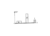
図6から図10は、複数のノイズ信号と小さな有効信号が存在する場合での増幅率調整最適化を示す。図6は、2つのノイズ信号S1とS2の存在することを示し、これらは有効信号Nよりも大きい。図7は、バンドフィルタBF2の上流での第1のスペクトルS1を示し、ハッチングにより相互変調積Iが、Rによりバックグランドノイズが示されている。図8には第2のスペクトルS2が示されており、このスペクトルはバンドフィルタBF2の下流で得られたものである。有効信号Nとノイズ信号S、バックグランドノイズRおよび相互変調積Iに対する比N/(S+R+I)が悪化していることがわかる。
【0023】
図9には、増幅率調整が最適に行われた後の経過が示されている。この増幅率調整は、第1の増幅器RV1の増幅率が比較的に低くなるように行われる。ノイズ信号S1,S2、有効信号Nおよび相互変調積Iの信号成分は小さくなる。しかし図10を図8と比較すると、ノイズ信号成分S1,S2と相互変調積Iが非常に小さくなっており、したがって比N/(S+R+I)は改善されている。信号強度検知器ユニットRSSIの出力電圧AS1は出力電圧AS2より格段に大きい。最適の増幅率調整はこの場合次の点で異なる。すなわち、まず比較的に低い増幅が行われ、続いて比較的に高い増幅が行われる点で異なる。図7〜図10からわかるように、このことにより比N/(S+R+I)が改善される。
【0024】
図11〜図17は、増幅率調整の改善に対する別の場合を示す。図11は、小さな有効信号Nと非常に小さなノイズ信号Sを示す。図12は、通常の増幅率によるスペクトルS1を示す。図13はスペクトルS2を示し、ここではバックグランドノイズRだけがノイズ成分として含まれていることがわかる。図14では、増幅器RV2によりさらに、有効信号NとバックグランドノイズRが増幅される。図15では、第1の増幅器RV1の増幅率が高められ、したがって有効信号Nが増大されるが、ノイズ信号Sも増大される。図16は、バンドフィルタBF2がノイズ信号Sを除去し、有効信号Nが完全に使用される例を示す。図17は、増幅器RV2によりさらに有効信号NとバックグランドノイズRが増幅される様子を示す。ここでは、バックグランドノイズが図14に示した大きさには増幅されない。これは増幅器RV1の増幅率を低減することにより得られる。この場合に、破線で示した第3の増幅器RV3を使用すれば、増幅器RV3の最大増幅によってバックグランドノイズをさらに低減することができる。このことが可能であるのは、出力電圧AS1が出力電圧AS2とほぼ同じ大きさだからである。
【0025】
図18〜図23は、隣接して大きなノイズ信号が存在するからチャネル変更した例を示す。図18は、入力信号ESを入力周波数finに依存して示す。帯域幅はBBにより示されている。ノイズ信号S1が有効信号Nに直接並んでいる。第1のスペクトルS1では、有効信号Nに相互変調積Iがかなりの割合で散乱していることがわかる。第2のスペクトルS2には、相互変調積Iが相変わらず存在している。出力電圧AS1は出力電圧AS2よりやや大きく、この場合はチャネルフィルタの上流で増幅器RV1の増幅率を比較的小さくする。図21は、チャネル変更を行った様子を示す。これにより、有効信号Nがノイズ信号Sから離れている。異なるチャネルはK1からK3により示されている。次に増幅器RV1の増幅率が比較的に小さくされ、これにより有効信号N、ノイズ信号S1および相互変調積Iが過度に大きくなることはない。図23のスペクトルS2は、有効信号Nがノイズ信号S1よりも格段に大きいことを示し、したがって出力電圧AS1は出力電圧AS2よりも格段に大きい。ここでは、チャネル変更によって出力電圧の改善の得られることが明らかである。
【0026】
図24は、図1に示された方法をアナログICに実現した実施例を示す。本発明に関連する構成部材には同じ部材符号が付してあり、機能は図1に示されたブロック回路と同じである。信号経路がIチャネルとQチャネルに分岐されていることがわかる。本発明の方法は、直交変調を行う通信システムにも適用することができる。制御ユニットはここでは別個に示されており、一方は第1の制御増幅器RV1とR’V1に対する増幅率コントロールユニットSE1に、他方は第2の制御可能な増幅器RV2と別の第2の制御可能な増幅器R’V2を制御する別のコントロールユニットSE2に配置されている。S、S’に対するそれぞれのスイッチは信号を信号強度検知ユニットRSSIに供給する。
【0027】
この回路の機能は、図1と図2から図23の線図に基づいて説明した機能に相応する。制御可能な増幅器RV3とミキサはこの図には示されておらず、考慮されていない。第1の制御可能な増幅器RV1,R’V1は、増幅器と第1のバンドフィルタBF1を有する。第2の制御可能な増幅器RV2,R’V2は複数の増幅器に分けられており、これにより比較的に大きな増幅率変化領域を可能にする。第1の制御可能な増幅器RV1,R’V1は、−6dBから+18dBの増幅率が可能であるように構成されている。
【0028】
第1の制御ユニットSE1は増幅係数Gain1とGain2により制御され、第2の制御ユニットSE2は電圧VAGCにより制御される。制御ユニットの一部はここの図示しないICに実現されている。この部分は、スイッチ位置をRSSIモードを介して制御する。したがってこの部分はスイッチ位置を知っており、信号強度検知ユニットRSSIがちょうどどのモードにあるかを知っている。すなわち、どの測定値ないし出力電圧がちょうど検出されるかを知っている。この部分は出力電圧ASを評価し、制御電圧Gain1、Gain2、VAGCを増幅率調整のために送出する。
【図面の簡単な説明】
【図1】本発明の方法に対するブロック回路図である。
【図2】特性曲線経過を示す線図である。
【図3】特性曲線経過を示す線図である。
【図4】特性曲線経過を示す線図である。
【図5】特性曲線経過を示す線図である。
【図6】特性曲線経過を示す線図である。
【図7】特性曲線経過を示す線図である。
【図8】特性曲線経過を示す線図である。
【図9】特性曲線経過を示す線図である。
【図10】特性曲線経過を示す線図である。
【図11】特性曲線経過を示す線図である。
【図12】特性曲線経過を示す線図である。
【図13】特性曲線経過を示す線図である。
【図14】特性曲線経過を示す線図である。
【図15】特性曲線経過を示す線図である。
【図16】特性曲線経過を示す線図である。
【図17】特性曲線経過を示す線図である。
【図18】特性曲線経過を示す線図である。
【図19】特性曲線経過を示す線図である。
【図20】特性曲線経過を示す線図である。
【図21】特性曲線経過を示す線図である。
【図22】特性曲線経過を示す線図である。
【図23】特性曲線経過を示す線図である。
【図24】本発明の方法に対する別のブロック回路図である。
【符号の説明】
ES 入力信号
BF1,BF2 バンドフィルタ
M ミキサ
NS 有効信号
RSSI 信号強度検知ユニット[0001]
BACKGROUND OF THE INVENTION
The invention starts from a method for improving the effective signal in a radio reception unit comprising a channel filter, a switch, a control unit and a signal strength detection unit.
[0002]
[Prior art]
It is known to use a signal strength detection unit to detect how large the ratio of the input signal and the subsequent effective signal is. The disadvantage here is that the noise components that are amplified together not only cause an error in the output signal of the signal strength detection unit, but also the quality of the effective signal.
[0003]
[Problems to be solved by the invention]
The object of the present invention is to provide a method for improving the effective signal in a radio receiving unit.
[0004]
[Means for Solving the Problems]
According to the present invention, the control unit controls the switch to supply the first signal to the signal strength detection unit alternately upstream of the channel filter and second signal downstream of the channel filter,
Supply the output signal of the signal strength detection unit to the control unit,
This is solved by configuring the amplifier to depend on the output signal.
[0005]
Advantageous refinements are described in the dependent claims.
[0006]
DETAILED DESCRIPTION OF THE INVENTION
The output signal is directly related to the effective signal to be improved. If the output signal is improved, the effective signal is also improved. If the output signal deteriorates, the effective signal also deteriorates.
[0007]
The amplifier is controlled to provide an improved effective signal by applying the method of the present invention by supplying the first and second signals, respectively, to the signal detection amplification unit and the comparator performed by the control unit. The
[0008]
The method of the present invention is further characterized in that the first signal includes an effective signal component and a noise signal component, and the noise signal component is extracted and filtered by the channel filter.
[0009]
By removing the noise signal by the channel filter, the signal strength with or without the noise signal can be evaluated.
[0010]
Furthermore, the method of the present invention is characterized in that the first amplifier amplifies the first signal upstream of the channel filter and the second amplifier amplifies the second signal downstream of the channel filter.
[0011]
By amplifying each signal with a plurality of amplifiers, optimization can be performed depending on how the two detection signals disappear. The optimization can then be carried out by the control unit with sufficient automation.
[0012]
The method of the invention is further characterized in that the amplification factor adjustment is optimized so that the ratio N / (S + R) of the effective signal N and the noise signal S and noise R is as large as possible.
[0013]
Normally, the first amplifier is operated with a large gain, thereby keeping the receiver noise small. However, by the method of the present invention, it can be detected that the amplification factor of the first amplifier is large and that there is a strong noise signal, so that only a small ratio N / (S + R) can be achieved. In this case, the improvement of the output signal is obtained by reducing the gain of the first amplifier and increasing the gain of the second amplifier.
[0014]
The method of the present invention further adjusts the maximum gain with the first amplifier and the relatively small gain with the second amplifier when the control unit detects that the valid signal is greater than the noise signal. It is characterized by adjusting.
[0015]
Furthermore, the present invention is characterized in that strong noise exists when the amplification factor of the first amplifier is minimum, and the frequency domain is changed when the ratio N / (S + R) of the output signal is small. .
[0016]
Even if the amplification factor of the first amplifier is small, when the quality of the output signal is still poor, the channel is changed, and the output signal is improved by increasing the effective signal compared to the noise.
[0017]
Instead of a switch for supplying various signals to the signal strength detection unit, it is also possible to use two signal strength detection units, which continuously supply two signals to the control unit.
[0018]
【Example】
Hereinafter, the present invention will be described in detail with reference to the drawings.
[0019]
FIG. 1 shows a block circuit diagram for the method of the present invention. The input signal ES reaches the second controllable amplifier RV2 via the first band filter BF1, the mixer M, the first controllable amplifier RV1, and the second band filter BF2. An effective signal NS is generated on the output side of the second amplifier. The valid signal NS is then supplied to the A / D converter. A third controllable amplifier RV3 can also be arranged between the first band filter BF1 and the mixer M. Since this third amplifier is not necessarily required, it is shown here in broken lines. The third controllable amplifier RV3 is used as an adjustment improvement unit. The control unit SE has a memory M. The memory is also indicated by a broken line. This is because the memory can exist outside the control unit SE. The control unit SE is further connected to a first controllable amplifier RV1, PLL circuit, a switch S, a second controllable amplifier RV2 and a signal strength detection unit RSSI. The PLL circuit is further connected to a mixer. If a third controllable amplifier RV3 is used, this amplifier is also connected to the control unit. The switch S supplies the first signal S1 to the signal strength detection unit RSSI upstream of the second band filter BF2 at the first switching position, and the second signal S2 to the second switching position at the second switching position. The signal strength detection unit RSSI is supplied downstream of the band filter BF2.
[0020]
A schematic curve is shown in the first band filter BF1 to which the input signal ES is supplied. This curve shows a bandwidth of 902-928 MHz. This bandwidth includes multiple receive channels. The valid signal is indicated by N in this bandwidth and the noise signal is indicated by S. The filtered input signal ES is then supplied to the mixer M. The mixer M mixes this signal with the signal from the PLL circuit, and further supplies the mixed signal to the second band filter BF2 via the first controllable amplifier VR1. The second band filter BF2 performs channel selection. Here, the channel filter used for channel selection is configured as a band filter. The switch S is controlled by the control unit SE and is first switched to the
[0021]
The function of FIG. 1 will be described based on the diagrams of FIGS. 2 to 5 show the basics of signal strength measurement. FIG. 2 shows the spectrum of the input signal ES as a function of the input frequency fin. The band filter BF1 limits the bandwidth of the ISM band (Industrial Scientific Medical) between 900 MHz and 930 MHz. An effective signal M and a noise signal S exist in this bandwidth. FIG. 3 shows the first spectrum S1 of the valid signal N and the noise signal S. The noise signal S is larger than the effective signal N. FIG. 4 shows the spectrum S2 of the valid signal N and the noise signal S smaller than this. FIG. 5 shows the output voltage AS depending on the signal strength of the input signal ES. The output voltage AS is directly proportional to the effective signal NS to be improved. If the output voltage AS is improved, the valid signal NS is also improved. If the output voltage AS deteriorates, the valid signal NS also deteriorates. The output voltage for spectrum S1 in FIG. 3 and the output voltage for spectrum S2 in FIG. 4 are denoted by AS1 and AS2, respectively. The characteristic curve K represents the curve of the characteristic curve of the signal strength detection unit RSSI. The output voltage AS1 for the spectrum S1 in FIG. 3 was obtained upstream of the band filter BF2. The output voltage AS2 for the spectrum S2 in FIG. 4 was obtained downstream of the band filter BF2. The difference value where the output voltage AS1 is greater than the output voltage AS2 is a measure for the strength of the noise signal in the adjacent channel.
[0022]
6 to 10 show amplification factor adjustment optimization in the case where there are a plurality of noise signals and a small effective signal. FIG. 6 shows that there are two noise signals S1 and S2, which are larger than the valid signal N. FIG. 7 shows the first spectrum S1 upstream of the band filter BF2, where the intermodulation product I is indicated by hatching and the background noise is indicated by R. FIG. 8 shows a second spectrum S2, which is obtained downstream of the band filter BF2. It can be seen that the ratio N / (S + R + I) to the effective signal N, the noise signal S, the background noise R, and the intermodulation product I is deteriorated.
[0023]
FIG. 9 shows a course after the gain adjustment is optimally performed. This amplification factor adjustment is performed so that the amplification factor of the first amplifier RV1 is relatively low. The signal components of the noise signals S1, S2, the effective signal N, and the intermodulation product I are small. However, comparing FIG. 10 with FIG. 8, the noise signal components S1 and S2 and the intermodulation product I are very small, and therefore the ratio N / (S + R + I) is improved. The output voltage AS1 of the signal strength detector unit RSSI is much larger than the output voltage AS2. The optimum gain adjustment in this case differs in the following points. That is, the difference is that a relatively low amplification is performed first, followed by a relatively high amplification. As can be seen from FIGS. 7-10, this improves the ratio N / (S + R + I).
[0024]
FIGS. 11-17 show another case for improving the gain adjustment. FIG. 11 shows a small valid signal N and a very small noise signal S. FIG. 12 shows a spectrum S1 with a normal amplification factor. FIG. 13 shows the spectrum S2, where it can be seen that only the background noise R is included as a noise component. In FIG. 14, the valid signal N and the background noise R are further amplified by the amplifier RV2. In FIG. 15, the amplification factor of the first amplifier RV1 is increased, so that the effective signal N is increased, but the noise signal S is also increased. FIG. 16 shows an example in which the band filter BF2 removes the noise signal S and the valid signal N is completely used. FIG. 17 shows how the valid signal N and the background noise R are further amplified by the amplifier RV2. Here, the background noise is not amplified to the magnitude shown in FIG. This is obtained by reducing the amplification factor of the amplifier RV1. In this case, if the third amplifier RV3 indicated by the broken line is used, the background noise can be further reduced by the maximum amplification of the amplifier RV3. This is possible because the output voltage AS1 is almost as large as the output voltage AS2.
[0025]
18 to 23 show an example in which the channel is changed because a large noise signal exists adjacently. FIG. 18 shows the input signal ES depending on the input frequency fin. The bandwidth is indicated by BB. The noise signal S1 is directly aligned with the effective signal N. In the first spectrum S1, it can be seen that the intermodulation product I is scattered in the effective signal N at a considerable rate. The intermodulation product I is still present in the second spectrum S2. The output voltage AS1 is slightly larger than the output voltage AS2, and in this case, the amplification factor of the amplifier RV1 is made relatively small upstream of the channel filter. FIG. 21 shows a state where a channel change is performed. Thereby, the effective signal N is separated from the noise signal S. Different channels are denoted by K1 to K3. Next, the amplification factor of the amplifier RV1 is made relatively small so that the effective signal N, the noise signal S1, and the intermodulation product I are not excessively increased. The spectrum S2 in FIG. 23 shows that the valid signal N is much larger than the noise signal S1, and therefore the output voltage AS1 is much larger than the output voltage AS2. Here, it is clear that improvement of the output voltage can be obtained by changing the channel.
[0026]
FIG. 24 shows an embodiment in which the method shown in FIG. 1 is implemented in an analog IC. Constituent members related to the present invention are denoted by the same reference numerals, and their functions are the same as those of the block circuit shown in FIG. It can be seen that the signal path is branched into an I channel and a Q channel. The method of the present invention can also be applied to a communication system that performs quadrature modulation. The control units are shown separately here, one for the gain control unit SE1 for the first control amplifiers RV1 and R′V1, and the other for the second controllable amplifier RV2 and another second controllable. It is arranged in a separate control unit SE2 that controls the amplifier R′V2. Each switch for S, S ′ supplies a signal to the signal strength detection unit RSSI.
[0027]
The function of this circuit corresponds to the function described on the basis of the diagrams of FIGS. 1 and 2 to 23. Controllable amplifier RV3 and mixer are not shown in this figure and are not considered. The first controllable amplifiers RV1, R′V1 have an amplifier and a first band filter BF1. The second controllable amplifiers RV2, R′V2 are divided into a plurality of amplifiers, thereby allowing a relatively large gain change region. The first controllable amplifiers RV1, R′V1 are configured to be capable of an amplification factor of −6 dB to +18 dB.
[0028]
The first control unit SE1 is controlled by the amplification coefficients Gain1 and Gain2, and the second control unit SE2 is controlled by the voltage VAGC. A part of the control unit is realized in an IC (not shown). This part controls the switch position via the RSSI mode. This part therefore knows the switch position and knows exactly which mode the signal strength detection unit RSSI is in. That is, it knows which measured value or output voltage is just detected. This part evaluates the output voltage AS and sends out control voltages Gain1, Gain2, and VAGC for adjusting the amplification factor.
[Brief description of the drawings]
FIG. 1 is a block circuit diagram for the method of the present invention.
FIG. 2 is a diagram showing the course of a characteristic curve.
FIG. 3 is a diagram showing the course of a characteristic curve.
FIG. 4 is a diagram showing the course of a characteristic curve.
FIG. 5 is a diagram showing the course of a characteristic curve.
FIG. 6 is a diagram showing the course of a characteristic curve.
FIG. 7 is a diagram showing a characteristic curve course;
FIG. 8 is a diagram showing the course of a characteristic curve.
FIG. 9 is a diagram showing the course of a characteristic curve.
FIG. 10 is a diagram showing the course of a characteristic curve.
FIG. 11 is a diagram showing the course of a characteristic curve.
FIG. 12 is a diagram showing the course of a characteristic curve.
FIG. 13 is a diagram showing the course of a characteristic curve.
FIG. 14 is a diagram showing the course of a characteristic curve.
FIG. 15 is a diagram showing the course of a characteristic curve.
FIG. 16 is a diagram showing the course of a characteristic curve.
FIG. 17 is a diagram showing the course of a characteristic curve.
FIG. 18 is a diagram showing the course of a characteristic curve.
FIG. 19 is a diagram showing the course of a characteristic curve.
FIG. 20 is a diagram showing the course of a characteristic curve.
FIG. 21 is a diagram showing the course of a characteristic curve.
FIG. 22 is a diagram showing the course of a characteristic curve.
FIG. 23 is a diagram showing the course of a characteristic curve.
FIG. 24 is another block circuit diagram for the method of the present invention.
[Explanation of symbols]
ES input signal BF1, BF2 Band filter M Mixer NS Valid signal RSSI Signal strength detection unit
Claims (4)
前記第1の制御可能な増幅器(RV1)はミキサ(M)とチャネルフィルタ(BF2)との間に接続されており、
前記第2の制御可能な増幅器(RV2)の入力端は前記チャネルフィルタ(BF2)の出力端に接続されており、
前記第3の制御可能な増幅器(RV3)は、前記第1のバンドパスフィルタ(BF1)と前記ミキサ(M)との間に接続されており、
前記制御ユニット(SE)は、前記第1から第3の制御可能な増幅器(RV1〜RV3)を制御する無線受信ユニットにおける有効信号を改善する方法において、
前記制御ユニット(SE)は前記スイッチ(S)を、当該スイッチ(S)がチャネルフィルタ(BF2)への入力信号(S1)と、該チャネルフィルタ(BF2)からの出力信号(S2)とを交互に前記信号強度検知ユニット(RSSI)に供給するように制御し、
前記スイッチ(S)が前記チャネルフィルタ(BF2)の前記入力信号(S1)を前記信号強度検知ユニット(RSSI)に供給するとき、該信号強度検知ユニット(RSSI)の出力は第1の出力電圧値(AS1)であり、
前記スイッチ(S)が前記チャネルフィルタ(BF2)の前記出力信号(S2)を前記信号強度検知ユニット(RSSI)に供給するとき、該信号強度検知ユニット(RSSI)の出力は第2の出力電圧値(AS2)であり、
前記第1の出力電圧値(AS1)と前記第2の出力電圧値(AS2)との差は、無線受信ユニットの受信隣接チャネルにおけるノイズ信号の強度に対する尺度であり、
前記信号強度検知ユニット(RSSI)の前記両出力電圧値(AS1,AS2)は出力信号として前記制御ユニット(SE)に供給され、
前記第1から第3の制御可能な増幅器(RV1,RV2,RV3)は前記制御ユニット(SE)により、前記信号強度検知ユニット(RSSI)の前記両出力電圧値(AS1,AS2)の関数として制御され、これにより前記有効信号が改善される、
ことを特徴とする、無線受信ユニットにおける有効信号を改善する方法。 First bandpass filter (BF1), mixer (M), channel filter (BF2), switch (S), control unit (SE), signal strength detection unit (RSSI), and first control A possible amplifier (RV1), a second controllable amplifier (RV2), and a third controllable amplifier (RV3) ;
The first controllable amplifier (RV1) is connected between a mixer (M) and a channel filter (BF2);
An input terminal of the second controllable amplifier (RV2) is connected to an output terminal of the channel filter (BF2) ;
The third controllable amplifier (RV3) is connected between the first bandpass filter (BF1) and the mixer (M);
In the method for improving the effective signal in the radio receiving unit for controlling the first to third controllable amplifiers (RV1 to RV3), the control unit (SE) comprises :
The control unit (SE) switches the switch (S), and the switch (S) alternately switches an input signal (S1) to the channel filter (BF2) and an output signal (S2) from the channel filter (BF2). To supply to the signal strength detection unit (RSSI),
When the switch (S) supplies the input signal (S1) of the channel filter (BF2) to the signal strength detection unit (RSSI), the output of the signal strength detection unit (RSSI) is a first output voltage value. (AS1),
When the switch (S) supplies the output signal (S2) of the channel filter (BF2) to the signal strength detection unit (RSSI), the output of the signal strength detection unit (RSSI) is a second output voltage value. (AS2),
The difference between the first output voltage value (AS1) and the second output voltage value (AS2) is a measure for the strength of the noise signal in the reception adjacent channel of the wireless reception unit;
The output voltage values (AS1, AS2) of the signal strength detection unit (RSSI) are supplied to the control unit (SE) as output signals,
The first to third controllable amplifiers (RV1, RV2 , RV3 ) are controlled by the control unit (SE) as a function of the output voltage values (AS1, AS2) of the signal strength detection unit (RSSI). This improves the effective signal,
A method for improving the useful signal in a radio receiving unit.
Applications Claiming Priority (2)
| Application Number | Priority Date | Filing Date | Title |
|---|---|---|---|
| DE19829500A DE19829500A1 (en) | 1998-07-02 | 1998-07-02 | Method for improving the useful signal in a radio receiving unit |
| DE19829500.6 | 1998-07-02 |
Publications (3)
| Publication Number | Publication Date |
|---|---|
| JP2000101372A JP2000101372A (en) | 2000-04-07 |
| JP2000101372A5 JP2000101372A5 (en) | 2006-08-17 |
| JP4510176B2 true JP4510176B2 (en) | 2010-07-21 |
Family
ID=7872703
Family Applications (1)
| Application Number | Title | Priority Date | Filing Date |
|---|---|---|---|
| JP18594599A Expired - Fee Related JP4510176B2 (en) | 1998-07-02 | 1999-06-30 | Method for improving effective signal in radio receiving unit |
Country Status (6)
| Country | Link |
|---|---|
| US (1) | US6370370B1 (en) |
| EP (1) | EP0969601B1 (en) |
| JP (1) | JP4510176B2 (en) |
| CN (1) | CN1151609C (en) |
| CA (1) | CA2276797C (en) |
| DE (2) | DE19829500A1 (en) |
Families Citing this family (17)
| Publication number | Priority date | Publication date | Assignee | Title |
|---|---|---|---|---|
| JP2000307972A (en) | 1999-04-26 | 2000-11-02 | Mitsubishi Electric Corp | Semiconductor integrated circuit |
| JP4608733B2 (en) * | 2000-05-10 | 2011-01-12 | 株式会社ニコン | Focus detection device |
| CN1270493C (en) * | 2000-09-25 | 2006-08-16 | 汤姆森特许公司 | Apparatus and method for optimizing the level of RF signals |
| US7710503B2 (en) | 2000-09-25 | 2010-05-04 | Thomson Licensing | Apparatus and method for optimizing the level of RF signals based upon the information stored on a memory |
| WO2002056490A2 (en) * | 2001-01-12 | 2002-07-18 | Qualcomm Inc | Direct conversion digital domain control |
| US6694129B2 (en) | 2001-01-12 | 2004-02-17 | Qualcomm, Incorporated | Direct conversion digital domain control |
| US6741844B2 (en) * | 2001-11-27 | 2004-05-25 | Motorola, Inc. | Receiver for audio enhancement and method therefor |
| US7212586B2 (en) * | 2002-01-18 | 2007-05-01 | Broadcom Corporation | Direct conversion RF transceiver for wireless communications |
| DE60315832T2 (en) * | 2002-06-07 | 2008-05-15 | Nxp B.V. | RECEPTION SIGNAL LEVEL INDICATION |
| US20040014438A1 (en) * | 2002-06-20 | 2004-01-22 | Abraham Hasarchi | System and method for excluding narrow band noise from a communication channel |
| US7460831B2 (en) | 2002-06-20 | 2008-12-02 | Dekolink Wireless Ltd. | System and method for excluding narrow band noise from a communication channel |
| US7042221B2 (en) * | 2002-07-31 | 2006-05-09 | Syracuse University | System and method for detecting a narrowband signal |
| US7596195B2 (en) * | 2004-03-31 | 2009-09-29 | Broadcom Corporation | Bandpass filter with reversible IQ polarity to enable a high side or low side injection receiver architecture |
| US7603098B2 (en) * | 2004-03-31 | 2009-10-13 | Broadcom Corporation | Programmable IF frequency filter for enabling a compromise between DC offset rejection and image rejection |
| US7778617B2 (en) * | 2007-03-30 | 2010-08-17 | Broadcom Corporation | Three stage algorithm for automatic gain control in a receiver system |
| KR20150070788A (en) * | 2013-12-17 | 2015-06-25 | 한국전자통신연구원 | Wideband rf receiver |
| US11437957B2 (en) * | 2021-02-01 | 2022-09-06 | Qualcomm Incorporated | Accelerated channel scanning with a two-point-modulated phase-locked loop |
Family Cites Families (13)
| Publication number | Priority date | Publication date | Assignee | Title |
|---|---|---|---|---|
| SE7512401L (en) * | 1974-11-07 | 1976-05-10 | Decca Ltd | DAMPING KIT FOR ANTENNA |
| DE2914092C2 (en) * | 1979-04-07 | 1983-02-10 | Rohde & Schwarz GmbH & Co KG, 8000 München | Arrangement for monitoring the overload of a high-frequency receiver |
| JPS59210734A (en) * | 1983-05-16 | 1984-11-29 | Toshiba Corp | Receiver |
| IL92021A (en) * | 1988-10-24 | 1994-06-24 | Hughes Aircraft Co | Automatic gain control (agc) for frequency hopping receiver |
| US5001776A (en) * | 1988-10-27 | 1991-03-19 | Motorola Inc. | Communication system with adaptive transceivers to control intermodulation distortion |
| JPH0338906A (en) * | 1989-07-05 | 1991-02-20 | Pioneer Electron Corp | Receiver |
| JPH03214931A (en) * | 1990-01-19 | 1991-09-20 | Matsushita Electric Ind Co Ltd | Receiver |
| US5339454A (en) * | 1991-08-05 | 1994-08-16 | Ford Motor Company | Automatic gain control for RF amplifier |
| DE4304819C2 (en) * | 1993-02-17 | 1994-11-17 | Vdo Schindling | Input circuit for a straight-ahead receiver |
| DE4319457C2 (en) * | 1993-06-11 | 1997-09-04 | Blaupunkt Werke Gmbh | Circuit arrangement for adjacent channel detection and suppression in an FM radio receiver |
| JP2821374B2 (en) * | 1994-08-31 | 1998-11-05 | 日本電気アイシーマイコンシステム株式会社 | Receiver |
| JPH08149021A (en) * | 1994-11-22 | 1996-06-07 | Nec Yamagata Ltd | Receiver front-end circuit |
| SE9601620L (en) * | 1996-04-29 | 1997-10-30 | Radio Design Innovation Tj Ab | Customizable radio receiver apparatus |
-
1998
- 1998-07-02 DE DE19829500A patent/DE19829500A1/en not_active Withdrawn
-
1999
- 1999-06-21 EP EP99111865A patent/EP0969601B1/en not_active Expired - Lifetime
- 1999-06-21 DE DE69937021T patent/DE69937021T2/en not_active Expired - Lifetime
- 1999-06-25 CN CNB991088867A patent/CN1151609C/en not_active Expired - Fee Related
- 1999-06-28 US US09/340,817 patent/US6370370B1/en not_active Expired - Lifetime
- 1999-06-30 CA CA2276797A patent/CA2276797C/en not_active Expired - Fee Related
- 1999-06-30 JP JP18594599A patent/JP4510176B2/en not_active Expired - Fee Related
Also Published As
| Publication number | Publication date |
|---|---|
| EP0969601A3 (en) | 2003-09-03 |
| CN1243361A (en) | 2000-02-02 |
| CA2276797C (en) | 2010-06-01 |
| EP0969601B1 (en) | 2007-09-05 |
| DE69937021T2 (en) | 2008-05-29 |
| CA2276797A1 (en) | 2000-01-02 |
| US6370370B1 (en) | 2002-04-09 |
| EP0969601A2 (en) | 2000-01-05 |
| DE69937021D1 (en) | 2007-10-18 |
| JP2000101372A (en) | 2000-04-07 |
| DE19829500A1 (en) | 2000-01-13 |
| CN1151609C (en) | 2004-05-26 |
Similar Documents
| Publication | Publication Date | Title |
|---|---|---|
| JP4510176B2 (en) | Method for improving effective signal in radio receiving unit | |
| US7383023B2 (en) | Communication apparatus | |
| JP4611496B2 (en) | Power amplifier circuit for load adjustment of adjacent and next adjacent channel power control | |
| JP4204589B2 (en) | Automatic gain controller | |
| US9037105B2 (en) | Dynamic gain assignment in analog baseband circuits | |
| CN101461134A (en) | Wide dynamic range amplifier gain control | |
| US20050020227A1 (en) | High frequency variable gain amplification device, control device, high frequency variable gain frequency-conversion device, and communication device | |
| KR100193842B1 (en) | Power Control Circuit and Method of Wireless Communication System | |
| JP4047274B2 (en) | Power adjustment type transmitter structure | |
| EP1710920A1 (en) | Receiving modulated radio signals | |
| US7929936B2 (en) | Receiver arrangement with AC coupling | |
| CN113258947A (en) | Device and method for reducing false signal amplitude of receiver | |
| JP3562472B2 (en) | Feed forward amplifier | |
| JP2001028553A (en) | Radio equipment and method for controlling thereof | |
| JPH03108817A (en) | Transmission output controller | |
| US20240348208A1 (en) | Power amplifier circuit and radio frequency circuit | |
| JP2001007669A (en) | Automatic gain control system | |
| JP5050341B2 (en) | Tuner circuit | |
| JPH05129845A (en) | Linear power amplifier | |
| KR100283172B1 (en) | Linearity improvement device and method of communication terminal | |
| JPS6220408A (en) | Automatic gain controller | |
| JPH0548346A (en) | Linear power amplifier circuit | |
| JP2689290B2 (en) | Wireless transmitter | |
| JPH0923176A (en) | Diversity device | |
| JP3515177B2 (en) | Station detection circuit |
Legal Events
| Date | Code | Title | Description |
|---|---|---|---|
| A521 | Request for written amendment filed |
Free format text: JAPANESE INTERMEDIATE CODE: A523 Effective date: 20060629 |
|
| A621 | Written request for application examination |
Free format text: JAPANESE INTERMEDIATE CODE: A621 Effective date: 20060629 |
|
| A131 | Notification of reasons for refusal |
Free format text: JAPANESE INTERMEDIATE CODE: A131 Effective date: 20090227 |
|
| A521 | Request for written amendment filed |
Free format text: JAPANESE INTERMEDIATE CODE: A523 Effective date: 20090527 |
|
| A131 | Notification of reasons for refusal |
Free format text: JAPANESE INTERMEDIATE CODE: A131 Effective date: 20090722 |
|
| A601 | Written request for extension of time |
Free format text: JAPANESE INTERMEDIATE CODE: A601 Effective date: 20091019 |
|
| A602 | Written permission of extension of time |
Free format text: JAPANESE INTERMEDIATE CODE: A602 Effective date: 20091022 |
|
| A521 | Request for written amendment filed |
Free format text: JAPANESE INTERMEDIATE CODE: A523 Effective date: 20100119 |
|
| TRDD | Decision of grant or rejection written | ||
| A01 | Written decision to grant a patent or to grant a registration (utility model) |
Free format text: JAPANESE INTERMEDIATE CODE: A01 Effective date: 20100401 |
|
| A01 | Written decision to grant a patent or to grant a registration (utility model) |
Free format text: JAPANESE INTERMEDIATE CODE: A01 |
|
| A61 | First payment of annual fees (during grant procedure) |
Free format text: JAPANESE INTERMEDIATE CODE: A61 Effective date: 20100430 |
|
| FPAY | Renewal fee payment (event date is renewal date of database) |
Free format text: PAYMENT UNTIL: 20130514 Year of fee payment: 3 |
|
| R150 | Certificate of patent or registration of utility model |
Free format text: JAPANESE INTERMEDIATE CODE: R150 |
|
| FPAY | Renewal fee payment (event date is renewal date of database) |
Free format text: PAYMENT UNTIL: 20140514 Year of fee payment: 4 |
|
| R250 | Receipt of annual fees |
Free format text: JAPANESE INTERMEDIATE CODE: R250 |
|
| R250 | Receipt of annual fees |
Free format text: JAPANESE INTERMEDIATE CODE: R250 |
|
| LAPS | Cancellation because of no payment of annual fees |