JP4509571B2 - Security elements and security documents with security elements - Google Patents
Security elements and security documents with security elements Download PDFInfo
- Publication number
- JP4509571B2 JP4509571B2 JP2003567680A JP2003567680A JP4509571B2 JP 4509571 B2 JP4509571 B2 JP 4509571B2 JP 2003567680 A JP2003567680 A JP 2003567680A JP 2003567680 A JP2003567680 A JP 2003567680A JP 4509571 B2 JP4509571 B2 JP 4509571B2
- Authority
- JP
- Japan
- Prior art keywords
- document
- layer
- security
- semi
- finished product
- Prior art date
- Legal status (The legal status is an assumption and is not a legal conclusion. Google has not performed a legal analysis and makes no representation as to the accuracy of the status listed.)
- Expired - Fee Related
Links
- 230000000694 effects Effects 0.000 claims abstract description 79
- 239000000758 substrate Substances 0.000 claims abstract description 41
- 239000011265 semifinished product Substances 0.000 claims description 31
- 229910052751 metal Inorganic materials 0.000 claims description 20
- 239000002184 metal Substances 0.000 claims description 20
- 239000000463 material Substances 0.000 claims description 19
- 238000010521 absorption reaction Methods 0.000 claims description 16
- 238000000034 method Methods 0.000 claims description 10
- 239000004922 lacquer Substances 0.000 claims description 7
- 230000002745 absorbent Effects 0.000 claims description 5
- 239000002250 absorbent Substances 0.000 claims description 5
- 238000000151 deposition Methods 0.000 claims description 3
- 238000004519 manufacturing process Methods 0.000 claims description 3
- 239000000047 product Substances 0.000 claims 1
- 239000010410 layer Substances 0.000 description 160
- 238000010586 diagram Methods 0.000 description 12
- 230000008859 change Effects 0.000 description 7
- 238000007740 vapor deposition Methods 0.000 description 7
- 230000000007 visual effect Effects 0.000 description 6
- 238000000576 coating method Methods 0.000 description 5
- 239000011241 protective layer Substances 0.000 description 5
- PXHVJJICTQNCMI-UHFFFAOYSA-N Nickel Chemical compound [Ni] PXHVJJICTQNCMI-UHFFFAOYSA-N 0.000 description 4
- KDLHZDBZIXYQEI-UHFFFAOYSA-N Palladium Chemical compound [Pd] KDLHZDBZIXYQEI-UHFFFAOYSA-N 0.000 description 4
- 239000000853 adhesive Substances 0.000 description 4
- 230000001070 adhesive effect Effects 0.000 description 4
- 239000012790 adhesive layer Substances 0.000 description 4
- 229910052782 aluminium Inorganic materials 0.000 description 4
- XAGFODPZIPBFFR-UHFFFAOYSA-N aluminium Chemical compound [Al] XAGFODPZIPBFFR-UHFFFAOYSA-N 0.000 description 4
- 229920003023 plastic Polymers 0.000 description 4
- 239000011248 coating agent Substances 0.000 description 3
- 150000001875 compounds Chemical class 0.000 description 3
- 230000001795 light effect Effects 0.000 description 3
- 230000003287 optical effect Effects 0.000 description 3
- 239000004033 plastic Substances 0.000 description 3
- XEEYBQQBJWHFJM-UHFFFAOYSA-N Iron Chemical compound [Fe] XEEYBQQBJWHFJM-UHFFFAOYSA-N 0.000 description 2
- UQSXHKLRYXJYBZ-UHFFFAOYSA-N Iron oxide Chemical compound [Fe]=O UQSXHKLRYXJYBZ-UHFFFAOYSA-N 0.000 description 2
- 230000005540 biological transmission Effects 0.000 description 2
- 238000005229 chemical vapour deposition Methods 0.000 description 2
- 238000009500 colour coating Methods 0.000 description 2
- 238000010438 heat treatment Methods 0.000 description 2
- 230000002452 interceptive effect Effects 0.000 description 2
- 229910052759 nickel Inorganic materials 0.000 description 2
- 229910052763 palladium Inorganic materials 0.000 description 2
- 238000005240 physical vapour deposition Methods 0.000 description 2
- 239000002985 plastic film Substances 0.000 description 2
- 229920006255 plastic film Polymers 0.000 description 2
- BASFCYQUMIYNBI-UHFFFAOYSA-N platinum Chemical compound [Pt] BASFCYQUMIYNBI-UHFFFAOYSA-N 0.000 description 2
- 229910052709 silver Inorganic materials 0.000 description 2
- 239000004332 silver Substances 0.000 description 2
- 238000004544 sputter deposition Methods 0.000 description 2
- 229910018072 Al 2 O 3 Inorganic materials 0.000 description 1
- OKTJSMMVPCPJKN-UHFFFAOYSA-N Carbon Chemical compound [C] OKTJSMMVPCPJKN-UHFFFAOYSA-N 0.000 description 1
- VYZAMTAEIAYCRO-UHFFFAOYSA-N Chromium Chemical compound [Cr] VYZAMTAEIAYCRO-UHFFFAOYSA-N 0.000 description 1
- 240000006829 Ficus sundaica Species 0.000 description 1
- KRHYYFGTRYWZRS-UHFFFAOYSA-M Fluoride anion Chemical compound [F-] KRHYYFGTRYWZRS-UHFFFAOYSA-M 0.000 description 1
- 239000004831 Hot glue Substances 0.000 description 1
- ZOKXTWBITQBERF-UHFFFAOYSA-N Molybdenum Chemical compound [Mo] ZOKXTWBITQBERF-UHFFFAOYSA-N 0.000 description 1
- OAICVXFJPJFONN-UHFFFAOYSA-N Phosphorus Chemical compound [P] OAICVXFJPJFONN-UHFFFAOYSA-N 0.000 description 1
- 229910004298 SiO 2 Inorganic materials 0.000 description 1
- VYPSYNLAJGMNEJ-UHFFFAOYSA-N Silicium dioxide Chemical compound O=[Si]=O VYPSYNLAJGMNEJ-UHFFFAOYSA-N 0.000 description 1
- BQCADISMDOOEFD-UHFFFAOYSA-N Silver Chemical compound [Ag] BQCADISMDOOEFD-UHFFFAOYSA-N 0.000 description 1
- 229910010413 TiO 2 Inorganic materials 0.000 description 1
- RTAQQCXQSZGOHL-UHFFFAOYSA-N Titanium Chemical compound [Ti] RTAQQCXQSZGOHL-UHFFFAOYSA-N 0.000 description 1
- 229910045601 alloy Inorganic materials 0.000 description 1
- 239000000956 alloy Substances 0.000 description 1
- 229910052799 carbon Inorganic materials 0.000 description 1
- 229910052804 chromium Inorganic materials 0.000 description 1
- 239000011651 chromium Substances 0.000 description 1
- BIJOYKCOMBZXAE-UHFFFAOYSA-N chromium iron nickel Chemical compound [Cr].[Fe].[Ni] BIJOYKCOMBZXAE-UHFFFAOYSA-N 0.000 description 1
- 229910017052 cobalt Inorganic materials 0.000 description 1
- 239000010941 cobalt Substances 0.000 description 1
- GUTLYIVDDKVIGB-UHFFFAOYSA-N cobalt atom Chemical compound [Co] GUTLYIVDDKVIGB-UHFFFAOYSA-N 0.000 description 1
- 230000002301 combined effect Effects 0.000 description 1
- 230000001419 dependent effect Effects 0.000 description 1
- 230000008021 deposition Effects 0.000 description 1
- 239000003989 dielectric material Substances 0.000 description 1
- 238000010894 electron beam technology Methods 0.000 description 1
- 238000004049 embossing Methods 0.000 description 1
- 239000011888 foil Substances 0.000 description 1
- 229910052732 germanium Inorganic materials 0.000 description 1
- GNPVGFCGXDBREM-UHFFFAOYSA-N germanium atom Chemical compound [Ge] GNPVGFCGXDBREM-UHFFFAOYSA-N 0.000 description 1
- PCHJSUWPFVWCPO-UHFFFAOYSA-N gold Chemical compound [Au] PCHJSUWPFVWCPO-UHFFFAOYSA-N 0.000 description 1
- 229910052737 gold Inorganic materials 0.000 description 1
- 239000010931 gold Substances 0.000 description 1
- 230000006872 improvement Effects 0.000 description 1
- AMGQUBHHOARCQH-UHFFFAOYSA-N indium;oxotin Chemical compound [In].[Sn]=O AMGQUBHHOARCQH-UHFFFAOYSA-N 0.000 description 1
- 230000006698 induction Effects 0.000 description 1
- 230000003993 interaction Effects 0.000 description 1
- 229910052742 iron Inorganic materials 0.000 description 1
- 238000000608 laser ablation Methods 0.000 description 1
- 150000002736 metal compounds Chemical class 0.000 description 1
- 229910001512 metal fluoride Inorganic materials 0.000 description 1
- 229910044991 metal oxide Inorganic materials 0.000 description 1
- 150000004706 metal oxides Chemical class 0.000 description 1
- 229910052976 metal sulfide Inorganic materials 0.000 description 1
- 229910052750 molybdenum Inorganic materials 0.000 description 1
- 239000011733 molybdenum Substances 0.000 description 1
- 229910052758 niobium Inorganic materials 0.000 description 1
- 239000010955 niobium Substances 0.000 description 1
- GUCVJGMIXFAOAE-UHFFFAOYSA-N niobium atom Chemical compound [Nb] GUCVJGMIXFAOAE-UHFFFAOYSA-N 0.000 description 1
- 150000004767 nitrides Chemical class 0.000 description 1
- 229910052698 phosphorus Inorganic materials 0.000 description 1
- 239000011574 phosphorus Substances 0.000 description 1
- 229910052697 platinum Inorganic materials 0.000 description 1
- 229910052573 porcelain Inorganic materials 0.000 description 1
- 238000003825 pressing Methods 0.000 description 1
- 230000008569 process Effects 0.000 description 1
- 238000004080 punching Methods 0.000 description 1
- 150000003346 selenoethers Chemical class 0.000 description 1
- 238000009958 sewing Methods 0.000 description 1
- 229910021332 silicide Inorganic materials 0.000 description 1
- FVBUAEGBCNSCDD-UHFFFAOYSA-N silicide(4-) Chemical compound [Si-4] FVBUAEGBCNSCDD-UHFFFAOYSA-N 0.000 description 1
- 229910052814 silicon oxide Inorganic materials 0.000 description 1
- 238000009751 slip forming Methods 0.000 description 1
- 239000010936 titanium Substances 0.000 description 1
- 229910052719 titanium Inorganic materials 0.000 description 1
- 238000002834 transmittance Methods 0.000 description 1
- 239000012780 transparent material Substances 0.000 description 1
- WFKWXMTUELFFGS-UHFFFAOYSA-N tungsten Chemical compound [W] WFKWXMTUELFFGS-UHFFFAOYSA-N 0.000 description 1
- 229910052721 tungsten Inorganic materials 0.000 description 1
- 239000010937 tungsten Substances 0.000 description 1
- 229910052720 vanadium Inorganic materials 0.000 description 1
- GPPXJZIENCGNKB-UHFFFAOYSA-N vanadium Chemical compound [V]#[V] GPPXJZIENCGNKB-UHFFFAOYSA-N 0.000 description 1
Images


Classifications
-
- G—PHYSICS
- G03—PHOTOGRAPHY; CINEMATOGRAPHY; ANALOGOUS TECHNIQUES USING WAVES OTHER THAN OPTICAL WAVES; ELECTROGRAPHY; HOLOGRAPHY
- G03H—HOLOGRAPHIC PROCESSES OR APPARATUS
- G03H1/00—Holographic processes or apparatus using light, infrared or ultraviolet waves for obtaining holograms or for obtaining an image from them; Details peculiar thereto
- G03H1/02—Details of features involved during the holographic process; Replication of holograms without interference recording
-
- B—PERFORMING OPERATIONS; TRANSPORTING
- B42—BOOKBINDING; ALBUMS; FILES; SPECIAL PRINTED MATTER
- B42D—BOOKS; BOOK COVERS; LOOSE LEAVES; PRINTED MATTER CHARACTERISED BY IDENTIFICATION OR SECURITY FEATURES; PRINTED MATTER OF SPECIAL FORMAT OR STYLE NOT OTHERWISE PROVIDED FOR; DEVICES FOR USE THEREWITH AND NOT OTHERWISE PROVIDED FOR; MOVABLE-STRIP WRITING OR READING APPARATUS
- B42D25/00—Information-bearing cards or sheet-like structures characterised by identification or security features; Manufacture thereof
- B42D25/20—Information-bearing cards or sheet-like structures characterised by identification or security features; Manufacture thereof characterised by a particular use or purpose
- B42D25/29—Securities; Bank notes
-
- G—PHYSICS
- G03—PHOTOGRAPHY; CINEMATOGRAPHY; ANALOGOUS TECHNIQUES USING WAVES OTHER THAN OPTICAL WAVES; ELECTROGRAPHY; HOLOGRAPHY
- G03H—HOLOGRAPHIC PROCESSES OR APPARATUS
- G03H1/00—Holographic processes or apparatus using light, infrared or ultraviolet waves for obtaining holograms or for obtaining an image from them; Details peculiar thereto
- G03H1/0005—Adaptation of holography to specific applications
- G03H1/0011—Adaptation of holography to specific applications for security or authentication
-
- G—PHYSICS
- G03—PHOTOGRAPHY; CINEMATOGRAPHY; ANALOGOUS TECHNIQUES USING WAVES OTHER THAN OPTICAL WAVES; ELECTROGRAPHY; HOLOGRAPHY
- G03H—HOLOGRAPHIC PROCESSES OR APPARATUS
- G03H1/00—Holographic processes or apparatus using light, infrared or ultraviolet waves for obtaining holograms or for obtaining an image from them; Details peculiar thereto
- G03H1/02—Details of features involved during the holographic process; Replication of holograms without interference recording
- G03H1/0252—Laminate comprising a hologram layer
- G03H1/0256—Laminate comprising a hologram layer having specific functional layer
-
- B—PERFORMING OPERATIONS; TRANSPORTING
- B42—BOOKBINDING; ALBUMS; FILES; SPECIAL PRINTED MATTER
- B42D—BOOKS; BOOK COVERS; LOOSE LEAVES; PRINTED MATTER CHARACTERISED BY IDENTIFICATION OR SECURITY FEATURES; PRINTED MATTER OF SPECIAL FORMAT OR STYLE NOT OTHERWISE PROVIDED FOR; DEVICES FOR USE THEREWITH AND NOT OTHERWISE PROVIDED FOR; MOVABLE-STRIP WRITING OR READING APPARATUS
- B42D25/00—Information-bearing cards or sheet-like structures characterised by identification or security features; Manufacture thereof
- B42D25/30—Identification or security features, e.g. for preventing forgery
- B42D25/328—Diffraction gratings; Holograms
-
- G—PHYSICS
- G03—PHOTOGRAPHY; CINEMATOGRAPHY; ANALOGOUS TECHNIQUES USING WAVES OTHER THAN OPTICAL WAVES; ELECTROGRAPHY; HOLOGRAPHY
- G03H—HOLOGRAPHIC PROCESSES OR APPARATUS
- G03H1/00—Holographic processes or apparatus using light, infrared or ultraviolet waves for obtaining holograms or for obtaining an image from them; Details peculiar thereto
- G03H1/02—Details of features involved during the holographic process; Replication of holograms without interference recording
- G03H1/024—Hologram nature or properties
- G03H1/0244—Surface relief holograms
-
- G—PHYSICS
- G03—PHOTOGRAPHY; CINEMATOGRAPHY; ANALOGOUS TECHNIQUES USING WAVES OTHER THAN OPTICAL WAVES; ELECTROGRAPHY; HOLOGRAPHY
- G03H—HOLOGRAPHIC PROCESSES OR APPARATUS
- G03H1/00—Holographic processes or apparatus using light, infrared or ultraviolet waves for obtaining holograms or for obtaining an image from them; Details peculiar thereto
- G03H1/02—Details of features involved during the holographic process; Replication of holograms without interference recording
- G03H1/0276—Replicating a master hologram without interference recording
- G03H1/028—Replicating a master hologram without interference recording by embossing
-
- G—PHYSICS
- G03—PHOTOGRAPHY; CINEMATOGRAPHY; ANALOGOUS TECHNIQUES USING WAVES OTHER THAN OPTICAL WAVES; ELECTROGRAPHY; HOLOGRAPHY
- G03H—HOLOGRAPHIC PROCESSES OR APPARATUS
- G03H1/00—Holographic processes or apparatus using light, infrared or ultraviolet waves for obtaining holograms or for obtaining an image from them; Details peculiar thereto
- G03H1/04—Processes or apparatus for producing holograms
- G03H1/18—Particular processing of hologram record carriers, e.g. for obtaining blazed holograms
- G03H2001/187—Trimming process, i.e. macroscopically patterning the hologram
-
- G—PHYSICS
- G03—PHOTOGRAPHY; CINEMATOGRAPHY; ANALOGOUS TECHNIQUES USING WAVES OTHER THAN OPTICAL WAVES; ELECTROGRAPHY; HOLOGRAPHY
- G03H—HOLOGRAPHIC PROCESSES OR APPARATUS
- G03H1/00—Holographic processes or apparatus using light, infrared or ultraviolet waves for obtaining holograms or for obtaining an image from them; Details peculiar thereto
- G03H1/22—Processes or apparatus for obtaining an optical image from holograms
- G03H1/2202—Reconstruction geometries or arrangements
- G03H2001/2223—Particular relationship between light source, hologram and observer
- G03H2001/2228—Particular relationship between light source, hologram and observer adapted for reflection and transmission reconstruction
-
- G—PHYSICS
- G03—PHOTOGRAPHY; CINEMATOGRAPHY; ANALOGOUS TECHNIQUES USING WAVES OTHER THAN OPTICAL WAVES; ELECTROGRAPHY; HOLOGRAPHY
- G03H—HOLOGRAPHIC PROCESSES OR APPARATUS
- G03H1/00—Holographic processes or apparatus using light, infrared or ultraviolet waves for obtaining holograms or for obtaining an image from them; Details peculiar thereto
- G03H1/22—Processes or apparatus for obtaining an optical image from holograms
- G03H1/2202—Reconstruction geometries or arrangements
- G03H2001/2223—Particular relationship between light source, hologram and observer
- G03H2001/2231—Reflection reconstruction
-
- G—PHYSICS
- G03—PHOTOGRAPHY; CINEMATOGRAPHY; ANALOGOUS TECHNIQUES USING WAVES OTHER THAN OPTICAL WAVES; ELECTROGRAPHY; HOLOGRAPHY
- G03H—HOLOGRAPHIC PROCESSES OR APPARATUS
- G03H1/00—Holographic processes or apparatus using light, infrared or ultraviolet waves for obtaining holograms or for obtaining an image from them; Details peculiar thereto
- G03H1/22—Processes or apparatus for obtaining an optical image from holograms
- G03H1/2202—Reconstruction geometries or arrangements
- G03H2001/2223—Particular relationship between light source, hologram and observer
- G03H2001/2234—Transmission reconstruction
-
- G—PHYSICS
- G03—PHOTOGRAPHY; CINEMATOGRAPHY; ANALOGOUS TECHNIQUES USING WAVES OTHER THAN OPTICAL WAVES; ELECTROGRAPHY; HOLOGRAPHY
- G03H—HOLOGRAPHIC PROCESSES OR APPARATUS
- G03H2223/00—Optical components
- G03H2223/12—Amplitude mask, e.g. diaphragm, Louver filter
-
- G—PHYSICS
- G03—PHOTOGRAPHY; CINEMATOGRAPHY; ANALOGOUS TECHNIQUES USING WAVES OTHER THAN OPTICAL WAVES; ELECTROGRAPHY; HOLOGRAPHY
- G03H—HOLOGRAPHIC PROCESSES OR APPARATUS
- G03H2250/00—Laminate comprising a hologram layer
- G03H2250/34—Colour layer
-
- G—PHYSICS
- G03—PHOTOGRAPHY; CINEMATOGRAPHY; ANALOGOUS TECHNIQUES USING WAVES OTHER THAN OPTICAL WAVES; ELECTROGRAPHY; HOLOGRAPHY
- G03H—HOLOGRAPHIC PROCESSES OR APPARATUS
- G03H2250/00—Laminate comprising a hologram layer
- G03H2250/36—Conform enhancement layer
-
- G—PHYSICS
- G03—PHOTOGRAPHY; CINEMATOGRAPHY; ANALOGOUS TECHNIQUES USING WAVES OTHER THAN OPTICAL WAVES; ELECTROGRAPHY; HOLOGRAPHY
- G03H—HOLOGRAPHIC PROCESSES OR APPARATUS
- G03H2250/00—Laminate comprising a hologram layer
- G03H2250/42—Reflective layer
Abstract
Description
【技術分野】
【0001】
本発明はセキュリティー素子、およびかかるセキュリティー素子を備えたセキュリティー・ドキュメント、特に、例えば銀行券のような有価証書に関するものである。また、本発明はかかるセキュリティー・ドキュメントの半製品に関するものでもある。特に、本発明はセキュリティー・ドキュメントに埋め込まれる所謂ウィンドウ・スレッドと呼ばれるセキュリティー・スレッド、およびセキュリティー・ドキュメントに貼付されるラベルまたは転写素子に関するものである。
【背景技術】
【0002】
本発明においてセキュリティー・ドキュメントという用語は特に銀行券を意味するが、小切手、小切手保証カード、クレジット・カード、身分証明書、パスポート、入場券、公共交通機関の乗車券等も含んでいる。前記セキュリティー・ドキュメントの半製品には、例えば、未印刷のセキュリティー・ペーパーおよびその他のセキュリティー・ドキュメントが該当する。
【0003】
一般に、前記セキュリティー・ドキュメントには、偽造防止および本物の証として、セキュリティー・スレッドが埋め込まれているか、またはセキュリティー・ラベルまたはセキュリティー転写素子が貼付されている。ウィンドウ・スレッド式のセキュリティー・スレッドは、例えば、銀行券のような有価証書に関連して広く知られているが、基本的には、小切手カード等にも適している。ウィンドウ・スレッドはセキュリティー・ドキュメントの基材に埋め込まれ周期的に表面に現れるため、これ等の“ウィンドウ領域”において視覚的に認識することができる。半透明の基材においては、所謂入射光/透過光効果により、透過光において、セキュリティー・スレッドは周囲の材料に対比して黒い縞模様として見える。しかし、入射光においては、セキュリティー・スレッドはウィンドウ領域においてのみ識別することができる。
【0004】
1つの表面にのみ現れる簡単なウィンドウ・スレッドと両面に現れる両面ウィンドウ・スレッドとの区別があり、以下、有価証書の両面に同時に現れる両面ウィンドウ・スレッドの1つの特別な場合をルックスルー・ウィンドウ・スレッドと呼ぶ。ルックスルー・ウィンドウ・スレッドは有価証書の穴または透明領域を越えて延びている。別の両面ウィンドウ・スレッドに、以下交互ウィンドウ・スレッドと呼ぶ、ドキュメントの表面または裏面に交互に現れるセキュリティー・スレッドがある。一般に、セキュリティー・スレッドとは別に、ドキュメントのギャップ、例えば、穴を越えて延びている所謂転写素子をセキュリティー素子として利用することができる。
【0005】
セキュリティー素子は、非常な努力を払わなければ偽造することができない複雑かつ目視および/または自動検査可能なセキュリティー機能を備えている。偽造防止機能を更に強化するため、かかるセキュリティー素子は、多くの場合、組み合わせることにより新たな効果をもたらすことができる幾つかの異なるセキュリティー機能を備えている。
【0006】
セキュリティー素子にしばしば見受けられる1つのセキュリティー機能に、視角および/または透過光あるいは入射光における観察によって色彩効果が変化する多層2色コーティングがある。この現象は、層材料の選択吸収特性と相まった層構造体の多重反射光および/または多重透過光の重複による干渉効果に基づくものである。視角による色彩の変化はカラーシフト効果とも呼ばれている。一方、入射光と透過光で交互に見たときの色彩の変化を以下色彩変化効果と呼ぶ。
【0007】
カラーシフト効果を有するセキュリティー素子に関連した光干渉コーティングが、例えば、特許文献1、特許文献2、特許文献3、および特許文献4に記載されている。層構造体の種類および層の数に応じ、2、3、4あるいはそれ以上の視角による色彩効果が得られる。かかるカラーシフト効果層の反射および透過特性は、幾つかの要因、特に、屈折率、吸収係数、層厚、および層構造体の層数に依存する。しかし、例えば、特許文献5に記載されているように、セキュリティー素子の干渉層を一体化し、全体を細分化して印刷用インクを混合することも同様に知られている。
【0008】
2色コーティングを有するセキュリティー素子が既に提案されているが、既存のセキュリティー素子と比較して、改良の必要性が依然として存在している。
【特許文献1】
欧州特許第0395410号明細書
【特許文献2】
欧州特許第0341002号明細書
【特許文献3】
国際公開第01/03945号パンフレット
【特許文献4】
米国特許第3858977号明細書
【特許文献5】
国際公開第00/31571号パンフレット
【発明の開示】
【発明が解決しようとする課題】
【0009】
従って、本発明の課題はセキュリティー素子を提供することであり、特に、従来の技術と比較して偽造防止機能を強化したセキュリティー・スレッドまたは転写素子を提供することである。
【課題を解決するための手段】
【0010】
前記課題は独立請求項の特徴を有する本発明のセキュリティー素子、セキュリティー・ドキュメント、および半製品によって解決される。従属請求項は本発明の特定の開発成果および実施の形態を示している。多層セキュリティー素子は、異なる角度から見たとき、前面および裏面の両方にカラーシフト効果をもたらす干渉層構造体を備えている。ここにおいて、セキュリティー素子の前面および裏面のカラーシフト効果は、同じようにすることも異なるようにすることもできる。
【0011】
複雑な多層構造体、およびそれによる再現が殆んど不可能なカラーシフト効果および色彩変化効果により、大変な努力を払わなければセキュリティー素子の偽造は不可能である。
【0012】
前記多層干渉構造体は少なくとも2つの多層干渉素子(I1、I2)、および少なくとも1つの反射層Rを備えている。
【0013】
前記多層干渉素子は吸収層と誘電体層とを重畳して形成され、幾つかの吸収層および誘電体層を交互に配することができる。吸収層と誘電体層とを交互に配する代わりに、屈折率が大きく異なる誘電体層のみを隣接して配置することによりカラーシフト効果を得ることもできる。しかし、吸収層を使用するとカラーシフト効果がより明らかになるため有利である。
【0014】
基本的に、干渉素子I1、I2は多層構造にすることができるが、各々が少なくとも2つの層、即ち、外側に配されている1つの吸収層A1またはA2、および対応する吸収層と内側に配されている反射層Rとの間に1つの誘電体層D1またはD2を備えていることが好ましい。一般に、吸収層A1、A2は、好ましくは厚さ4〜20nmのクロム、鉄、金、アルミニウム、またはチタンのような材料から成る金属層である。ニッケルクロム鉄化合物のような化合物、またはバナジウム、パラジウム、あるいはモリブデンのようなレアメタルも吸収層の材料として用いることができる。更に別の適材は、例えば、特許文献3に記載されており、例えば、ニッケル、コバルト、タングステン、ニオブ、アルミニウム、金属フッ化物、金属酸化物、金属硫化物、金属窒化物、金属炭化物、金属リン化物、金属セレン化物、金属珪化物のような金属化合物およびこれらの化合物、炭素、ゲルマニウム、陶性合金、酸化鉄等である。
【0015】
干渉素子の吸収層A1、A2は、干渉層構造体において、同一または異なる厚さを有することができると共に/または同一または異なる吸収材料から成ることができる。
【0016】
誘電体層D1、D2は、例えば、SiO2,MgF、SiOx(1<x<2)およびAl2O3のような屈折率が1.7未満の透明材料が主として用いられる。基本的に、蒸着可能な大半の透明化合物が使用可能であり、特にZrO2、ZnS、TiO2、およびインジウム錫酸化物(ITO)のような屈折率の高いコーティング材料も使用できる。誘電体層D1、D2に適する別の材料は、例えば、特許文献3に記載されている。誘電体層D1、D2の層厚は100〜1000nmの範囲であり、200〜500nmが好ましい。
【0017】
干渉素子の誘電体層は、干渉層構造体において、同一または異なる厚さを有することができると共に/または同一または異なる誘電体材料から成ることができる。
【0018】
干渉素子は干渉層構造体において異なるカラーシフト効果をもたらすよう設計されていることが好ましい。
【0019】
吸収層A1、A2の代わりに、誘電体層を用いることもできるが、隣接誘電体層の屈折率nが大きく異なり、一方においてn<1.7、他方においてn>1.7であり明確なカラーシフト効果が得られるようにする必要がある。前記構造体において明確なカラーシフト効果を得るためには幾つかの誘電体層が必要であり、そのために製造コストが非常に高くなるので吸収層を使用することが好ましい。
【0020】
干渉素子I1、I2の吸収層A1、A2、誘電体層D1、D2、および反射層Rは、セキュリティー素子1の構成要素となるか、または単に仲介担体としてのみ機能し、後にセキュリティー素子が目的物に貼付されるときに除去される基体Sの上に真空蒸着法によって形成されることが好ましい。
【0021】
殆んどの蒸着法が前記層の形成に適している。蒸発槽、抵抗加熱による蒸着、誘導加熱による蒸着、あるいは電子ビーム蒸着、スパッタリング(DCまたはAC)およびアーク蒸着による物理気相成長法(PVD)が1つのグループを形成する。更に、前記蒸着は、例えば、反応プラズマ中におけるスパッタリングまたはその他のプラズマ励起蒸着法のような化学気相成長法(CVD)によっても可能である。基本的には、前記誘電体層を印刷することもできる。
【0022】
反射層Rは、例えば、アルミニウム、銀、ニッケル、プラチナ、あるいはパラジウムから成る金属層であることが好ましく、銀、アルミニウム、あるいはその他光を強く反射する材料から成ることが好ましい。反射層Rの反射特性が優れていればいるほど、より著しいカラーシフト効果と、ときにより用いられるレリーフ構造体の卓越した回折効果が得られる。
【0023】
反射層は厚さに応じ不透明にも半透明にもすることができる。本明細書において、“半透明”という用語は、反射層の光透過率が90%未満、好ましくは80〜20%であることを意味する。
【0024】
前記セキュリティー素子は反射層によって分離された2つの干渉素子を備え、各々の素子が視角によるカラーシフト効果をもたらすことが好ましい。半透明反射層を用いると色彩変化効果も得られる可能性がある。セキュリティー素子が、好ましくは透明の基体を備えている場合には、干渉素子および反射層Rは基体の同じ面に配される。2つの干渉層を基体のそれぞれ別の面に配する場合には、2つの反射層を用いる必要がある。この場合、セキュリティー素子の層は、干渉素子(I1)、反射層(R1)、基体(S)、反射層(R2)、および干渉素子(I2)の順となる。
【0025】
干渉素子の構造は同じであっても異なっていてもよく、従って、セキュリティー素子を見る側に応じた色の相互作用が同じであっても異なっていてもよいが、異なるカラーシフト効果が好ましい。異なるカラーシフト効果は、例えば、各々の干渉素子および反射層に異なる材料を使用すると共に/または各々の干渉素子または反射層の個々の層厚を違えることによって得られる。干渉素子の背後に配されている反射金属層によって、カラーシフト効果による色強度が最大限向上するため、本セキュリティー素子は目視検査が容易である。
【0026】
更に、前記セキュリティー素子は、特に、少なくとも部分的に反射層に重複する回折構造体を備えることができる。前記反射層は、前記回折構造体の視覚効果も増大するため、本セキュリティー素子も目視検査が容易である。
【0027】
回折構造体として、例えば、回折パターン、透過ホログラム、体積ホログラム、あるいは反射ホログラムがあるが、格子構造体も考えられる。格子構造体は干渉素子および反射層を担持する基体の構成要素であることが好ましいが、適切な層と層との間に配するか、また付加層に配することもできる。前記付加層は、例えば、ラッカー層である。
【0028】
前記回折構造体は、セキュリティー素子を形成する透明プラスチック基体表面に、とりわけエンボス加工を施し、反射ホログラムとして配し、前記反射層が前記反射ホログラムの反射背面を成すことが好ましい。反射層を挟んでいる2つの干渉素子は、いずれもプラスチック基体のレリーフ構造体がエンボス加工されている面、または反対側の平坦な面の一方に配することができる。しかし、前記干渉層は前記基体の両面に配しても差支えない。この場合、前記基体は前記レリーフ構造体を有している面およびその反対側の平坦な面にそれぞれ1つの反射層を備える必要がある。従って、異なる視覚効果を有する幾つかの形態が考えられ、多かれ少なかれ、使用目的に応じて選択することができる。
【0029】
いずれの観察面においても、前記セキュリティー素子の視覚効果は実質的に干渉素子の色彩効果によって決定される。回折構造体が別に用いられている場合には、少なくとも1つの観察面において、または適切な層構成により両方の観察面において、視覚上の外観はこれらの回折構造体の視覚効果によって実質的に決定される。この場合、前記2つのセキュリティー機能が互いに重複する。
【0030】
従って、前記セキュリティー素子は、各々の観察面において、特に目視検査可能な独特のセキュリティー特性を識別することができるため、特に両面セキュリティー・スレッドとして適している。前記両面セキュリティー・スレッドは、セキュリティー・ドキュメントの対向する表面の異なる場所に現れるか、または少なくとも目に見える交互セキュリティー・スレッドとして使用することができる。しかし、前記セキュリティー・スレッドは、特に薄い領域または透明領域においてドキュメントの両方の側から見えるか、またはドキュメントの穴を越えて延びているルックスルー・ウィンドウ・スレッドとして使用することもできる。
【0031】
しかし、前記セキュリティー素子は、例えば、セキュリティー・ドキュメント表面の穴の上に配されるラベルまたはパッチのような転写素子としても適している。前記ドキュメントを一方の側から見ると、カラーシフト効果を有するパッチとしての視覚的印象を受ける。前記ドキュメントの穴を通し別の側から前記パッチの一部を見ると、別のカラーシフト効果または、場合により、同じカラーシフト効果が現れる。場合により備えられている回折模様が、両方の側から見えるか、または一方の側からのみ見ることができるかについては、セキュリティー素子の層構造そのものに依存する。
【0032】
本明細書において“転写素子”という用語は、例えば、プラスチック・フィルムのような別の担体層上に、後にセキュリティー・ペーパーに取り付けられたときと逆の順序に形成され、所望の外形を有する接着層またはラッカー層を用いてセキュリティー・ペーパーに転写されるセキュリティー素子を意味する。セキュリティー素子の形状には制限がなく、輪つなぎ飾り等の繊細な構造体まで可能である。前記セキュリティー素子は、有価証書の縁部と平行に延びるストライプとして形成される場合が多い。転写した後、転写素子の担体層はセキュリティー素子の層構造体から剥離するか、またはそのまま保護層として残すことができる。
【0033】
個々に分離され輪郭を有している個別素子として転写素子を担体層に形成することができる。別の方法として、担体層上に転写素子の層系列を連続的に形成する。互いに距離を置いて配されている個別転写素子または連続した層構造体を備えている前記担体層を以下“転写材料”と呼び、担体層上に配されている層系列を“転写層”と呼ぶ。
【0034】
連続転写層の場合、転写材料は接着層によってセキュリティー・ペーパーに接着される。前記接着層はそれぞれのエンボス加工具によって活性化されるため、活性化された転写層領域のみがセキュリティー・ペーパーに接着される。他の領域は担体層と共にすべて剥離される。別の方法として、前記接着層を転写するセキュリティー素子の形状と同じにすることができる。接着剤としてホットメルト接着剤を用いることが好ましい。しかし、反応性ラッカーのようなその他すべての接着剤を使用することができる。
【0035】
本発明に基づいて形成されるセキュリティー素子は、別のセキュリティー機能、特に、反射層および/または干渉素子を局部的に除去したネガティブまたはポジティブ筆跡と組み合せることができる。多層干渉素子構造体においては、少なくとも1つの層からすべての層に至るまで局部的に除去することができる。例えば、少なくとも1つの吸収層および少なくとも1つの誘電体層を備える干渉素子においては、前記ギャップが吸収層に設けられることが好ましい。セキュリティー素子に2つの干渉素子が配される場合、各々の素子を別の設計とすることができる。例えば、1つの干渉素子に数字を組み込んで吸収層のギャップによって見えるようにし、別の干渉素子に文字を組み込んで吸収層のギャップによって見えるようにすることができる。ここにおいて、設計に関わる制限は一切ない。前記筆跡は英数字であることが好ましいが、これに限定されるものではない。本発明においては、表示可能なすべてのパターン、記号、または符号を含んでいる。層構造体のギャップにより、更なる入射光/透過光効果が得られる。二重干渉コーティングにより前記効果は特に顕著となる。何故なら、簡単な干渉コーティングと比較して、パターン、記号、あるいは符号が入射光において更に見え難くなるからである。しかし、透過光においては、前記ギャップは暗い周囲を背景に明るい領域として識別することができる。
【0036】
反射層、および状況に応じ干渉素子を局部的に除去することにより、個別層の設計に応じてセキュリティー素子が部分的に透明または半透明になる。
【発明を実施するための最良の形態】
【0037】
以下、前記特性および個々の形態におけるそれぞれの効果について添付図面を参照しながら説明する。図は本発明を分かり易くするためのものであり、必ずしも実際の寸法に対応しているとは限らない。
【0038】
個々の図に関する技術的説明は、その図に示されている特定の実施の形態に限定されるものではなく、本発明の一般的構想の説明にも当てはまるものである。
【0039】
図1は、2つのセキュリティー素子2および4を備えている、例えば、紙製の銀行券またはプラスチック製の身分証明書のようなセキュリティー・ドキュメント1を示す図である。第1セキュリティー素子2は、ドキュメント1表面の穴またはその他の透明領域3の上に、例えば、接着剤によってラベルまたは転写素子として貼付されているパッチである。第2セキュリティー素子4は、交互ウィンドウ・スレッドまたはルックスルー・ウィンドウ・スレッドとしてドキュメント1に埋め込まれている両面ウィンドウ・セキュリティー・スレッドである。
【0040】
図2〜4は、セキュリティー素子2および4の貼付および埋め込み方法の例を示している。図2は図1のセキュリティー・ドキュメント1のパッチを貫いて延びているII−II線断面図である。ドキュメント1の穴3を囲む領域にパッチ2に覆われているプリント模様5がある。前記穴は、例えば、製紙の段階、または後に紙を押し抜くことにより作成することができる。セキュリティー素子2の層構造体の金属反射層により、プリント模様5はパッチ2の下に隠されている。従って、本発明の1つの好ましい実施の形態において、前記領域の反射層を半透明にするかまたは反射層を設けないことにより、パッチ2が透明または少なくとも半透明になり下に隠れているプリント模様5が少なくとも特定の視角において識別できるようにしている。前記とは別に、パッチ2の穴3の領域は両方の側から見ることができる。
【0041】
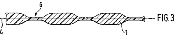
図3は、ルックスルー・ウィンドウ・スレッドとしての図1のウィンドウ・セキュリティー・スレッドを示す図である。例えば、銀行券であるドキュメント1は、更に、非常に薄く形成され極端な場合には穴であるウィンドウ領域6を有しているため、セキュリティー・スレッド4は両方の側から見ることができる。従って、ルックスルー・ウィンドウ領域6は、ルックスルー・ウィンドウ・スレッド4に対し、パッチ2に対する穴3と同じ機能を有している。
【0042】
図4は、例えば、プラスチック製の身分証明書であるドキュメント1の交互両面ウィンドウ・セキュリティー・スレッドとしての図1のウィンドウ・セキュリティー・スレッド4を示す図である。前記のようなカードに、例えば、フラップを打ち抜くことができる。前記カードを曲げることによりセキュリティー・スレッド4を縫うようにして前記フラップを通過させ、次いでカードが自身の弾性によって平面に戻ることができるため、交互両面ウィンドウ・スレッドとしてスレット4をカードに組み込むことができる。
【0043】
両面交互ウィンドウ・スレッドを、例えば、銀行券に埋め込む方法は、当業者周知である。
【0044】
図5〜8は、本発明のセキュリティー素子2または4の各種層構成を示す部分断面図である。
【0045】
図5は、金属不透明反射層Rを挟んで2つの干渉素子I1およびI2が基体Sの一方の面に隣接して重畳されている層構成を示す図である。前記基体の反対側の表面にはホログラフィック・レリーフ・パターン8がエンボス加工されている。別の方法として、レリーフ・パターン8は、基体のいずれか一方の面に配される別のラッカー層にエンボス加工することもできる。機械的負荷に弱いレリーフ構造体8は、光学保護層Cによって周囲のストレスから保護されている。
【0046】
各々が1つの吸収層と誘電体層とから成る干渉素子I1およびI2は、例えば、視角による緑色とマゼンタとの間の2色カラーシフト効果を呈する。各々の吸収層A1およびA2、並びに誘電体層D1およびD2がそれぞれ同じ材料から成り、層の厚さが同じであれば、セキュリティー素子は前面および裏面において同じカラーシフト効果を呈する。
【0047】
前記のようなセキュリティー・ドキュメントを上部干渉素子I1の側から見ると、金属反射層Rによって鮮明なカラーシフト効果が現れる。前記観察方向からはホログラム効果は生じない。前記セキュリティー素子を反対側、即ち、基体側から見ると、カラーシフト効果のみならず、回折構造体8による回折効果も現れる。従って、図5の層構造体は全体として、1つの観察面においてホログラム効果とカラーシフト効果とが組み合わされた効果が得られ、他方の観察面において回折効果が重複されていないカラーシフト効果が得られる。
【0048】
図6は本発明の第2の実施の形態による前記と同様の層構成を示す図である。この層構成においては、レリーフ構造体8が下部干渉素子I2に直接隣接している点が図5の層構成と異なっている。干渉素子I1およびI2は、それぞれ層厚が1μm未満(図は単に層構成を図解しているに過ぎない)であるため、反射層Rは表面に層が蒸着されるレリーフ構造体8と同じレリーフ・パターンを有している。その結果、図5の層構造体とは異なり、レリーフ構造体8によるホログラム効果が両方の観察面に現れる。図6の層構成において、干渉素子I1およびI2が同様に形成されている場合、回折効果およびカラーシフト効果が両方の面において殆んど同じであるため、特に両面セキュリティー・スレッドとして適している。従って、セキュリティー・スレッドを埋め込む場合、面を気にする必要がない。
【0049】
図7は、干渉素子I1とI2とがそれぞれ基体Sの対向する面に配されている、本発明のセキュリティー素子の第3の実施の形態による層構成を示す図である。この実施の形態においては、2つの金属反射層R1およびR2がそれぞれ基体の1つの面に配されている。即ち、反射層R2がレリーフ構造体を備えている基体の面に配され、反射層R1がレリーフ構造体8と反対側の平坦な面に配されている。その結果、この場合も図5の実施の形態同様、ホログラム効果は一方の側にのみ現れる。干渉素子I1が担持されている側からセキュリティー素子を見ると、回折効果は現れないが、干渉素子I2が担持されている側から見ると現れる。しかし、本実施の形態においては、干渉素子I2がレリーフ構造体8の前に配されているため、セキュリティー素子の両面にカラーシフト効果が現れる。干渉素子I1およびI2の構造を違えることにより、異なるカラーシフト効果を得ることができる。本実施の形態のセキュリティー素子を作製する場合、基体の各々の面にそれぞれの層を蒸着することができる。しかし、各々が1つの反射層および干渉層を有する2つのフィルムを最初に蒸着し、次いで、蒸着面が外を向くようにしてこれらのフィルムを積層することもできる。
【0050】
別の実施の形態において、図7の基体両面に回折構造体をエンボス加工し、回折効果が両方の観察面に現れるようにすることができる。この場合、異なる回折構造体を基体の各々の面にエンボス加工することにより、視角によって異なる回折パターンが現れるようにすることもできる。
【0051】
図8は、金属反射層Rがギャップ9を有し、セキュリティー素子のギャップ9領域が透明または少なくとも半透明になるようにした、図5の層構造を有する本発明の実施の形態を示す図である。これにより、入射光/透過光効果が得られる。前記セキュリティー素子を、例えば、セキュリティー・スレッドとして銀行券に埋め込むと、記号、パターン、あるいは符号形状を成すことができるギャップ9は入射光において殆んど知覚できない。しかし、これらのギャップ9は透過光で見ると明るい領域としてセキュリティー・スレッドの別の暗く見える部分から浮き出て見える。基体S側から見ると、入射光および透過光においてカラーシフト効果が現れる。更に、透過光において前記ギャップを識別することができる。回折構造体8により、入射光または透過光において、反射層を背景とする領域に回折効果が現れる。透過光において、前記ギャップ領域の回折効果が完全に弱まる。前記基体と反対の側から見ると回折効果は現れない。入射光および透過光において、カラーシフト効果が知覚され、透過光において更に前記ギャップが知覚される。
【0052】
一般に、および本明細書に記載のすべての実施の形態において、基体Sは透明であることが好ましく、有色透明または有色透明にコーティングしたものも可能である。基体Sはレリーフ構造体がエンボス加工され、干渉素子I1、I2、および反射金属層が干渉素子I1とI2との間にコーティングされた後、帯、スレッド、またはラベル状に切断される軟質プラスチック・フィルムであることが好ましい。また、基体Sは転写フィルムに存在し、転写方法、例えば、箔押しによってドキュメントに転写することができる。それ故、図5〜8の層構造体に保護層、特に接着層、およびカバー層を付加し、カバー層を除去した後セキュリティー素子をラベルとして目的物に接着するか、または転写方法によって転写素子として転写することができる。
【0053】
反射層Rのギャップ9はレーザー・アブレーションによって形成することができる。しかし、金属反射層Rを蒸着する前に可溶性インクを用いて基体Sに印刷を施し、その後のプロセスにおいて前記可溶性インクを上に重畳されている金属反射層Rと共に除去することができる。ギャップ9を形成するための別の多くの方法は当業者周知である。
【0054】
基体Sのコーティングが終了してからギャップ9領域の金属層Rを除去することにより、反射層Rのみならず、隣接する干渉素子I1、および状況に応じて干渉素子I2も除去することができる。このようにして、透過光においてギャップが完全に無色に見えるようにすることができる。
【0055】
図9は図5の層構成から基体のレリーフ・パターンおよび保護層Cを除いた本発明の実施の形態を示す図である。金属反射層Rが半透明であるため、セキュリティー素子そのものが半透明である。このことは、本実施の形態において、セキュリティー素子の両面においてカラーシフト効果および、場合により、更に色彩変化効果が現れることを意味している。干渉素子I1およびI2の設計が異なる場合には、異なるカラーシフト効果または色彩変化効果をもたらし、反射層Rの半透明性によりこれらの効果が互いに重複し、セキュリティー素子が複雑な外観を呈することができる。干渉素子I1が“マゼンタ”から“緑色”に変化するカラーシフト効果を有し、干渉素子I2が“緑色”から“黄色”に変化するカラーシフト効果を有し、観察者が干渉層構造体を特定の側から見ると、両方の効果が現れるが、これらの効果は互いに重複しそれぞれの色が混ぜ合わされた総合効果として現れる。デザインにもよるが、通常、観察者に近い側の干渉素子は、観察者から遠い側の干渉素子と比較して前記総合効果のより大きな部分を占め、半透明層によって効果が弱められる。
【図面の簡単な説明】
【0056】
【図1】 穴の上に貼付されているセキュリティー素子、およびウィンドウ・スレッドとして一体化されているセキュリティー素子を備えたセキュリティー・ドキュメントを示す図。
【図2】 図1のセキュリティー・ドキュメントのII−II線断面図。
【図3】 ルックスルー・ウィンドウ・スレッドを備えた図1のセキュリティー・ドキュメントのIII−III線断面図。
【図4】 両面交互ウィンドウ・セキュリティー・スレッドを備えた図1のセキュリティー・ドキュメントのIV−IV線断面図。
【図5】 第1の実施の形態によるセキュリティー素子の層構成を示す図。
【図6】 第2の実施の形態によるセキュリティー素子の層構成を示す図。
【図7】 第3の実施の形態によるセキュリティー素子の層構成を示す図。
【図8】 反射層にギャップを有している図5のセキュリティー素子の層構成を示す図。
【図9】 第4の実施の形態によるセキュリティー素子の層構成を示す図。
【符号の説明】
【0057】
1 セキュリティー・ドキュメント
2、4 セキュリティー素子
3 穴
5 プリント模様
6 ウィンドウ領域
8 レリーフ・パターン
A1、A2 吸収層
D1、D2 誘電体層
I1、12 干渉素子
S 基体
C 光学保護層【Technical field】
[0001]
The present invention relates to a security element and a security document provided with such a security element, in particular a value certificate such as a bank note. The invention also relates to a semi-finished product of such a security document. In particular, the present invention relates to a security thread called a so-called window thread embedded in a security document, and a label or transfer element attached to the security document.
[Background]
[0002]
In the present invention, the term “security document” particularly means a bank note, but also includes a check, a check guarantee card, a credit card, an identification card, a passport, an admission ticket, a public transport ticket, and the like. Examples of the semi-finished product of the security document include unprinted security paper and other security documents.
[0003]
In general, the security document is embedded with a security thread or a security label or a security transfer element as an anti-counterfeiting and authentic proof. A window thread type security thread is widely known in connection with a security certificate such as a bank note, but is basically suitable for a check card or the like. Since window threads are embedded in the security document substrate and periodically appear on the surface, they can be visually recognized in these “window areas”. In a translucent substrate, due to the so-called incident / transmitted light effect, in the transmitted light, the security thread appears as a black striped pattern compared to the surrounding material. However, for incident light, security threads can only be identified in the window area.
[0004]
There is a distinction between simple window threads that appear only on one surface and double-sided window threads that appear on both sides, and in the following one special case of double-sided window threads that appear simultaneously on both sides of a certificate is a look-through window. Called a thread. The look-through window thread extends beyond the hole or transparent area of the certificate. Another double-sided window thread is a security thread that appears alternately on the front or back side of the document, hereinafter referred to as an alternating window thread. In general, apart from a security thread, a so-called transfer element that extends beyond a document gap, eg, a hole, can be used as a security element.
[0005]
The security element has a complex and visually and / or automatically inspectable security function that cannot be counterfeited without great effort. In order to further enhance the anti-counterfeiting function, such security elements often have several different security functions that can be combined to produce new effects.
[0006]
One security feature often found in security elements is a multi-layer, two-color coating whose color effect changes with viewing angle and / or observation in transmitted or incident light. This phenomenon is based on the interference effect due to the overlap of the multiple reflected light and / or multiple transmitted light of the layer structure combined with the selective absorption characteristics of the layer material. The change in color depending on the viewing angle is also called the color shift effect. On the other hand, a change in color when viewed alternately with incident light and transmitted light is hereinafter referred to as a color change effect.
[0007]
Optical interference coatings related to security elements having a color shift effect are described in, for example,
[0008]
Although security elements having a two-color coating have already been proposed, there remains a need for improvement compared to existing security elements.
[Patent Document 1]
European Patent No. 0395410
[Patent Document 2]
European Patent No. 034002
[Patent Document 3]
International Publication No. 01/03945 Pamphlet
[Patent Document 4]
US Pat. No. 3,858,977
[Patent Document 5]
International Publication No. 00/31571 Pamphlet
DISCLOSURE OF THE INVENTION
[Problems to be solved by the invention]
[0009]
Accordingly, an object of the present invention is to provide a security element, and in particular, to provide a security thread or transfer element that has an enhanced anti-counterfeit function as compared with the prior art.
[Means for Solving the Problems]
[0010]
The object is solved by a security element, security document and semi-finished product according to the invention having the features of the independent claims. The dependent claims indicate specific development results and embodiments of the present invention. The multilayer security element comprises an interference layer structure that provides a color shift effect on both the front and back surfaces when viewed from different angles. Here, the color shift effects of the front surface and the back surface of the security element can be the same or different.
[0011]
Due to the complex multi-layer structure and the color shift and color change effects that are almost impossible to reproduce, it is impossible to forge the security element without great efforts.
[0012]
The multilayer interference structure comprises at least two multilayer interference elements (I 1 , I 2 ), And at least one reflective layer R.
[0013]
The multilayer interference element is formed by overlapping an absorption layer and a dielectric layer, and several absorption layers and dielectric layers can be alternately arranged. Instead of alternately arranging the absorption layer and the dielectric layer, it is possible to obtain a color shift effect by arranging only the dielectric layers having greatly different refractive indexes adjacent to each other. However, the use of an absorption layer is advantageous because the color shift effect becomes more apparent.
[0014]
Basically, interference element I 1 , I 2 Can have a multilayer structure, but each has at least two layers, i.e. one absorbent layer A arranged on the outside 1 Or A 2 And one dielectric layer D between the corresponding absorbing layer and the reflective layer R disposed inside 1 Or D 2 It is preferable to provide. In general, absorption layer A 1 , A 2 Is a metal layer made of a material such as chromium, iron, gold, aluminum or titanium, preferably 4 to 20 nm thick. A compound such as a nickel chromium iron compound or a rare metal such as vanadium, palladium, or molybdenum can also be used as the material of the absorption layer. Further suitable materials are described in, for example,
[0015]
Absorption layer A of interference element 1 , A 2 Can have the same or different thickness in the interference layer structure Ki And / or can consist of the same or different absorbent materials.
[0016]
Dielectric layer D 1 , D 2 For example, SiO 2 , MgF, SiOx (1 <x <2) and Al 2 O 3 A transparent material having a refractive index of less than 1.7 is mainly used. Basically, most transparent compounds that can be deposited can be used, in particular ZrO. 2 , ZnS, TiO 2 And high refractive index coating materials such as indium tin oxide (ITO) can also be used. Dielectric layer D 1 , D 2 Another material suitable for is described in
[0017]
The dielectric layer of the interference element can have the same or different thickness in the interference layer structure. Ki And / or can be made of the same or different dielectric materials.
[0018]
The interference elements are preferably designed to provide different color shift effects in the interference layer structure.
[0019]
Absorbent layer A 1 , A 2 Alternatively, a dielectric layer can be used, but the refractive index n of the adjacent dielectric layer is greatly different, n <1.7 on one side and n> 1.7 on the other side, and a clear color shift effect is obtained. Need to be able to. In order to obtain a clear color shift effect in the structure, several dielectric layers are required, which makes it very expensive to manufacture, so it is preferable to use an absorbing layer.
[0020]
Interference element I 1 , I 2 Absorption layer A 1 , A 2 , Dielectric layer D 1 , D 2 , And the reflective layer R, which serves as a component of the
[0021]
Most vapor deposition methods are suitable for forming the layer. Evaporator, vapor deposition by resistance heating, vapor deposition by induction heating, or physical vapor deposition (PVD) by electron beam vapor deposition, sputtering (DC or AC) and arc vapor deposition form one group. Further, the vapor deposition can be performed by chemical vapor deposition (CVD), such as sputtering in reactive plasma or other plasma enhanced vapor deposition. Basically, the dielectric layer can also be printed.
[0022]
The reflective layer R is preferably a metal layer made of, for example, aluminum, silver, nickel, platinum, or palladium, and is preferably made of silver, aluminum, or another material that strongly reflects light. The better the reflective properties of the reflective layer R, the more pronounced color shift effect and the superior diffraction effect of the relief structure used sometimes.
[0023]
The reflective layer can be opaque or translucent depending on the thickness. In this specification, the term “translucent” means that the light transmittance of the reflective layer is less than 90%, preferably 80 to 20%.
[0024]
Preferably, the security element includes two interference elements separated by a reflective layer, and each element provides a color shift effect depending on the viewing angle. If a translucent reflective layer is used, a color change effect may also be obtained. If the security element comprises a preferably transparent substrate, the interference element and the reflective layer R are arranged on the same surface of the substrate. When two interference layers are arranged on different surfaces of the substrate, it is necessary to use two reflection layers. In this case, the layer of the security element is an interference element (I 1 ), Reflective layer (R 1 ), Substrate (S), reflective layer (R) 2 ), And interference elements (I 2 ) In that order.
[0025]
The structure of the interference element may be the same or different, and therefore the color interaction depending on the viewing side of the security element may be the same or different, but different color shift effects are preferred. Different color shift effects can be obtained, for example, by using different materials for each interference element and reflective layer and / or by varying the individual layer thickness of each interference element or reflective layer. Since the reflective metal layer disposed behind the interference element maximizes the color intensity due to the color shift effect, the security element can be easily visually inspected.
[0026]
Furthermore, the security element can in particular comprise a diffractive structure that at least partially overlaps the reflective layer. Since the reflection layer also increases the visual effect of the diffractive structure, the security element can be easily visually inspected.
[0027]
Examples of the diffractive structure include a diffraction pattern, a transmission hologram, a volume hologram, and a reflection hologram, but a grating structure is also conceivable. The grating structure is preferably a component of the substrate carrying the interference element and the reflective layer, but can also be arranged between suitable layers or in additional layers. The additional layer is, for example, a lacquer layer.
[0028]
The diffractive structure is preferably embossed on the surface of the transparent plastic substrate forming the security element and arranged as a reflection hologram, and the reflection layer forms the reflection back surface of the reflection hologram. The two interference elements sandwiching the reflective layer can be arranged either on the surface on which the relief structure of the plastic substrate is embossed or on the opposite flat surface. However, the interference layer may be disposed on both sides of the substrate. In this case, it is necessary that the base has one reflective layer on each of the surface having the relief structure and the flat surface on the opposite side. Thus, several forms with different visual effects are conceivable and can be selected more or less depending on the intended use.
[0029]
In any observation plane, the visual effect of the security element is substantially determined by the color effect of the interference element. If diffractive structures are used separately, the visual appearance is substantially determined by the visual effect of these diffractive structures, at least on one viewing surface, or on both viewing surfaces with appropriate layer configuration. Is done. In this case, the two security functions overlap each other.
[0030]
Accordingly, the security element is particularly suitable as a double-sided security thread because it can identify unique security characteristics that can be visually inspected on each observation surface. The double-sided security thread may appear at different locations on opposite surfaces of the security document, or at least be used as a visible alternating security thread. However, the security thread can also be used as a look-through window thread that is visible from both sides of the document, particularly in thin or transparent areas, or that extends beyond a hole in the document.
[0031]
However, the security element is also suitable as a transfer element such as a label or patch placed over a hole in the security document surface. When the document is viewed from one side, it receives a visual impression as a patch having a color shift effect. Viewing a portion of the patch through the hole in the document from another side will show another color shift effect, or possibly the same color shift effect. Whether the optional diffraction pattern is visible from both sides or only from one side depends on the layer structure of the security element itself.
[0032]
As used herein, the term “transfer element” refers to an adhesive that is formed on another carrier layer, such as a plastic film, in the reverse order that it was later attached to the security paper and has the desired profile. Means a security element that is transferred to a security paper using a layer or lacquer layer. There are no restrictions on the shape of the security element, and it is possible to use delicate structures such as a looping ornament. The security element is often formed as a stripe that extends parallel to the edge of the certificate. After the transfer, the carrier layer of the transfer element can be peeled off from the layer structure of the security element or left as a protective layer.
[0033]
The transfer elements can be formed in the carrier layer as individual elements which are individually separated and have contours. Alternatively, a layer sequence of transfer elements is continuously formed on the carrier layer. The carrier layer having individual transfer elements or continuous layer structures arranged at a distance from each other is hereinafter referred to as “transfer material”, and the layer sequence arranged on the carrier layer is referred to as “transfer layer”. Call.
[0034]
In the case of a continuous transfer layer, the transfer material is adhered to the security paper by an adhesive layer. Since the adhesive layer is activated by the respective embossing tool, only the activated transfer layer region is adhered to the security paper. All other areas are peeled off with the carrier layer. Alternatively, the shape of the security element to which the adhesive layer is transferred can be made the same. It is preferable to use a hot melt adhesive as the adhesive. However, all other adhesives such as reactive lacquers can be used.
[0035]
Security elements formed in accordance with the present invention can be combined with other security features, particularly negative or positive handwriting with the reflective layer and / or interference elements removed locally. In the multilayer interference element structure, it can be locally removed from at least one layer to all layers. For example, in an interference element including at least one absorption layer and at least one dielectric layer, the gap is preferably provided in the absorption layer. When two interference elements are arranged in the security element, each element can be designed differently. For example, a number can be incorporated into one interfering element so that it is visible through the gap in the absorbing layer, and a letter can be incorporated into another interfering element so that it is visible through the gap in the absorbing layer. Here, there are no design-related restrictions. The handwriting is preferably alphanumeric, but is not limited thereto. In the present invention, all patterns, symbols or symbols that can be displayed are included. Due to the gap in the layer structure, further incident / transmitted light effects are obtained. The effect is particularly pronounced by the double interference coating. This is because patterns, symbols, or signs are more difficult to see in incident light compared to simple interference coatings. However, in transmitted light, the gap can be identified as a bright area against a dark surrounding.
[0036]
Depending on the reflective layer and the local removal of the interference element depending on the situation, the security element becomes partially transparent or translucent depending on the design of the individual layers.
BEST MODE FOR CARRYING OUT THE INVENTION
[0037]
Hereinafter, the characteristics and respective effects in the individual embodiments will be described with reference to the accompanying drawings. The drawings are provided to facilitate understanding of the present invention and do not necessarily correspond to actual dimensions.
[0038]
The technical description for an individual figure is not limited to the specific embodiment shown in that figure, but also applies to the description of the general concept of the invention.
[0039]
FIG. 1 shows a
[0040]
2 to 4 show examples of the attaching and embedding methods of the
[0041]
FIG. 3 is a diagram illustrating the window security thread of FIG. 1 as a look-through window thread. For example, the
[0042]
FIG. 4 is a diagram illustrating the window security thread 4 of FIG. 1 as an alternating double-sided window security thread for
[0043]
Methods for embedding double-sided alternating window threads, for example, in banknotes are well known to those skilled in the art.
[0044]
5 to 8 are partial cross-sectional views showing various layer configurations of the
[0045]
FIG. 5 shows two interference elements I sandwiching a metal opaque reflective layer R. 1 And I 2 2 is a diagram showing a layer configuration in which is superimposed adjacent to one surface of a substrate S. FIG. A
[0046]
Interference elements I each consisting of one absorption layer and a dielectric layer 1 And I 2 Exhibits, for example, a two-color color shift effect between green and magenta depending on the viewing angle. Each absorption layer A 1 And A 2 , And dielectric layer D 1 And D 2 Are made of the same material and have the same layer thickness, the security element exhibits the same color shifting effect on the front and back surfaces.
[0047]
The above-described security document is transferred to the upper interference element I. 1 When viewed from the side, the metal reflection layer R exhibits a clear color shift effect. The hologram effect does not occur from the viewing direction. When the security element is viewed from the opposite side, that is, from the substrate side, not only the color shift effect but also the diffraction effect by the
[0048]
FIG. 6 is a diagram showing a layer structure similar to that described above according to the second embodiment of the present invention. In this layer structure, the
[0049]
FIG. 7 shows the interference element I 1 And I 2 FIG. 6 is a diagram showing a layer configuration according to the third embodiment of the security element of the present invention, in which each is arranged on the opposing surface of the substrate S. In this embodiment, two metal reflective layers R1 and R2 are respectively disposed on one surface of the substrate. That is, the reflective layer R 2 Is disposed on the surface of the substrate having the relief structure, and the reflective layer R 1 Is arranged on a flat surface opposite to the
[0050]
In another embodiment, diffractive structures can be embossed on both sides of the substrate of FIG. 7 so that the diffraction effect appears on both viewing surfaces. In this case, different diffractive structures may be embossed on each surface of the substrate so that different diffraction patterns appear depending on the viewing angle.
[0051]
FIG. 8 is a diagram showing an embodiment of the present invention having the layer structure of FIG. 5 in which the metal reflective layer R has a gap 9 and the gap 9 region of the security element is transparent or at least translucent. is there. Thereby, the incident light / transmitted light effect is obtained. When the security element is embedded in a bank note as a security thread, for example, the gap 9 that can form a symbol, pattern, or code shape is hardly perceivable in incident light. However, these gaps 9 appear to emerge from another dark portion of the security thread as a bright area when viewed in transmitted light. When viewed from the substrate S side, a color shift effect appears in incident light and transmitted light. Furthermore, the gap can be identified in the transmitted light. Due to the
[0052]
In general, and in all embodiments described herein, the substrate S is preferably transparent, and may be colored transparent or colored transparent coated. The substrate S is embossed with a relief structure, and the interference element I 1 , I 2 , And the reflective metal layer is the interference element I 1 And I 2 It is preferably a soft plastic film that is coated between the two and then cut into strips, threads, or labels. The substrate S is present on the transfer film and can be transferred to the document by a transfer method, for example, foil pressing. Therefore, a protective layer, in particular, an adhesive layer and a cover layer are added to the layer structure of FIGS. Can be transferred as.
[0053]
The gap 9 of the reflective layer R can be formed by laser ablation. However, it is possible to print the substrate S using the soluble ink before depositing the metal reflective layer R, and to remove the soluble ink together with the metal reflective layer R superimposed thereon in a subsequent process. Many other methods for forming the gap 9 are well known to those skilled in the art.
[0054]
By removing the metal layer R in the gap 9 region after the coating of the substrate S is completed, not only the reflective layer R but also the adjacent interference element I 1 And, depending on the situation, interference element I 2 Can also be removed. In this way, the gap can be made completely colorless in the transmitted light.
[0055]
FIG. 9 is a diagram showing an embodiment of the present invention in which the relief pattern of the substrate and the protective layer C are removed from the layer configuration of FIG. Since the metal reflective layer R is translucent, the security element itself is translucent. This means that in this embodiment, a color shift effect and, in some cases, a color change effect appears on both sides of the security element. Interference element I 1 And I 2 If the designs are different, different color shift effects or color change effects are brought about, and these effects overlap each other due to the translucency of the reflective layer R, and the security element can have a complicated appearance. Interference element I 1 Has a color shift effect that changes from “magenta” to “green”, and the interference element I 2 Has a color shift effect that changes from “green” to “yellow”, and when the observer sees the interference layer structure from a certain side, both effects appear, but these effects overlap each other and each color Appears as a combined effect. Although depending on the design, the interference element on the side closer to the observer usually occupies a larger portion of the total effect than the interference element on the side far from the observer, and the effect is weakened by the translucent layer.
[Brief description of the drawings]
[0056]
FIG. 1 shows a security document with a security element affixed over a hole and a security element integrated as a window thread.
FIG. 2 is a cross-sectional view of the security document of FIG. 1 taken along line II-II.
3 is a cross-sectional view taken along line III-III of the security document of FIG. 1 with a look-through window thread.
FIG. 4 is a view of the security document of FIG. 1 with a double-sided alternating window security thread. IV − IV FIG.
FIG. 5 is a diagram showing a layer configuration of a security element according to the first embodiment.
FIG. 6 is a diagram showing a layer configuration of a security element according to a second embodiment.
FIG. 7 is a diagram showing a layer configuration of a security element according to a third embodiment.
8 is a diagram showing a layer configuration of the security element of FIG. 5 having a gap in the reflective layer.
FIG. 9 is a diagram showing a layer configuration of a security element according to a fourth embodiment.
[Explanation of symbols]
[0057]
1 Security document
2, 4 Security element
3 holes
5 Print pattern
6 Window area
8 Relief pattern
A 1 , A 2 Absorption layer
D 1 , D 2 Dielectric layer
I 1 1 2 Interference element
S substrate
C Optical protective layer
Claims (29)
前記2つの面を見たとき、それぞれ識別可能であると共にカラーシフト効果が該両面に現れるよう前記セキュリティー素子が取り付けられており、
前記セキュリティー素子が、カラーシフト効果を備えた少なくとも2つの多層干渉素子および該少なくとも2つの多層干渉素子に挟まれた少なくとも1つの反射層を有していることを特徴とするドキュメントまたは半製品。A security document comprising opposing first and second surfaces and a security element (2, 4), or a semi-finished product of the security document,
The security element is attached so that each of the two surfaces can be identified and a color shift effect appears on the two surfaces when viewed.
A document or semi-finished product, wherein the security element has at least two multilayer interference elements having a color shift effect and at least one reflective layer sandwiched between the at least two multilayer interference elements .
該転写材料が、カラーシフト効果を備えた少なくとも2つの多層干渉素子および少なくとも1つの反射層を有しているとともに、
担体層、
反射層(R)、および
該反射層(R)の両面に備えられた、カラーシフト効果を有する多層干渉素子(I1、I2)
を有して成るか、または
担体層、
基体(S)、および
該基体(S)の両面に備えられた、反射層(R1、R2)およびカラーシフト効果を有する多層干渉素子(I1、I2)であって、該基体(S)と該多層干渉素子(I 1 、I 2 )とで該反射層(R 1 、R 2 )を挟むように設けた多層干渉素子(I 1 、I 2 )
を有して成ることを特徴とする材料。A transfer material for attaching a security element to a certificate,
The transfer material has at least two multilayer interference elements with color shift effect and at least one reflective layer;
Carrier layer,
Reflective layer (R), and multilayer interference element (I 1 , I 2 ) having a color shift effect provided on both sides of reflective layer (R)
Or comprising a carrier layer,
Substrate (S), and provided on both surfaces of the base body (S), a reflective layer (R 1, R 2) and a multilayer interference element with a color shift effect (I 1, I 2), said substrate ( S) and multilayer interference element (I 1, I 2) the de the reflective layer (R 1, multilayer interference element provided so as to sandwich the R 2) (I 1, I 2)
A material characterized by comprising:
担体層を提供するステップ、および
少なくとも1つの反射層およびカラーシフト効果を有する少なくとも2つの多層干渉素子を、該多層干渉素子で該反射層を挟むように蒸着するステップ
の各ステップを有して成ることを特徴とする方法。A method for producing a transfer material for attaching a security element to a certificate,
Providing a carrier layer, and depositing at least one reflective layer and at least two multilayer interference elements having a color shift effect so as to sandwich the reflective layer between the multilayer interference elements. A method characterized by that.
Applications Claiming Priority (2)
| Application Number | Priority Date | Filing Date | Title |
|---|---|---|---|
| DE10206357A DE10206357A1 (en) | 2002-02-14 | 2002-02-14 | Security element and security document with such a security element |
| PCT/EP2003/001383 WO2003068525A1 (en) | 2002-02-14 | 2003-02-12 | Security element and security document with one such security element |
Publications (3)
| Publication Number | Publication Date |
|---|---|
| JP2005516829A JP2005516829A (en) | 2005-06-09 |
| JP2005516829A5 JP2005516829A5 (en) | 2006-04-13 |
| JP4509571B2 true JP4509571B2 (en) | 2010-07-21 |
Family
ID=27634997
Family Applications (1)
| Application Number | Title | Priority Date | Filing Date |
|---|---|---|---|
| JP2003567680A Expired - Fee Related JP4509571B2 (en) | 2002-02-14 | 2003-02-12 | Security elements and security documents with security elements |
Country Status (11)
| Country | Link |
|---|---|
| US (1) | US7699350B2 (en) |
| EP (1) | EP1476315B2 (en) |
| JP (1) | JP4509571B2 (en) |
| CN (1) | CN100567022C (en) |
| AT (1) | ATE556862T1 (en) |
| AU (1) | AU2003208837B2 (en) |
| CA (1) | CA2476213C (en) |
| DE (1) | DE10206357A1 (en) |
| RU (1) | RU2297919C2 (en) |
| UA (1) | UA76591C2 (en) |
| WO (1) | WO2003068525A1 (en) |
Families Citing this family (78)
| Publication number | Priority date | Publication date | Assignee | Title |
|---|---|---|---|---|
| US20070195392A1 (en) * | 1999-07-08 | 2007-08-23 | Jds Uniphase Corporation | Adhesive Chromagram And Method Of Forming Thereof |
| CN1666888B (en) * | 2000-01-21 | 2011-12-14 | 光学涂层实验公司 | Optically variable security devices |
| US11768321B2 (en) | 2000-01-21 | 2023-09-26 | Viavi Solutions Inc. | Optically variable security devices |
| TWI334382B (en) | 2003-07-14 | 2010-12-11 | Flex Products Inc | Vacuum roll coated security thin film interference products with overt and/or covert patterned layers |
| DE102004003984A1 (en) † | 2004-01-26 | 2005-08-11 | Giesecke & Devrient Gmbh | Lattice image with one or more grid fields |
| AT504587A1 (en) * | 2004-02-16 | 2008-06-15 | Hueck Folien Gmbh | IMPACT-SAFE SAFETY FEATURE WITH COLOR TIP EFFECT |
| DE102004014778A1 (en) * | 2004-03-26 | 2005-10-13 | Leonard Kurz Gmbh & Co. Kg | Security and / or value document |
| EP2287011B1 (en) * | 2004-04-30 | 2017-06-28 | Giesecke & Devrient GmbH | Security element and process for manufacturing it |
| DE102004031043A1 (en) * | 2004-06-25 | 2006-01-12 | Giesecke & Devrient Gmbh | Security element with introduced motives |
| DE102004032565A1 (en) * | 2004-07-05 | 2006-02-16 | Giesecke & Devrient Gmbh | Security element with color shift effect |
| AU2005274464C1 (en) * | 2004-08-12 | 2013-07-25 | Giesecke+Devrient Currency Technology Gmbh | Security element comprising a support |
| JP4564535B2 (en) | 2004-09-15 | 2010-10-20 | クレイン アンド カンパニー インコーポレーテッド | Security device and new anti-counterfeit product using this device |
| CN1600988A (en) * | 2004-09-24 | 2005-03-30 | 孙显林 | Anti-fraud material |
| DE102004049118A1 (en) | 2004-10-07 | 2006-04-13 | Giesecke & Devrient Gmbh | Security element and method for its production |
| EP1652688A1 (en) | 2004-10-29 | 2006-05-03 | Arjowiggins Security | Security device |
| DE102005022018A1 (en) * | 2005-05-12 | 2006-11-16 | Giesecke & Devrient Gmbh | Security paper and process for its production |
| DE102005027380B4 (en) * | 2005-06-14 | 2009-04-30 | Ovd Kinegram Ag | The security document |
| FR2893424B1 (en) | 2005-11-16 | 2008-01-25 | Arjowiggins Soc Par Actions Si | OPTICAL STRUCTURE, IN PARTICULAR FOR A DOCUMENT OF SECURITY AND / OR VALUE. |
| DE102005061749A1 (en) | 2005-12-21 | 2007-07-05 | Giesecke & Devrient Gmbh | Optically variable security element for making valuable objects safe has an achromatic reflecting micro-structure taking the form of a mosaic made from achromatic reflecting mosaic elements |
| CA2580321C (en) * | 2006-03-06 | 2014-11-04 | Jds Uniphase Corporation | Security devices incorporating optically variable adhesive |
| US8139292B2 (en) * | 2006-04-12 | 2012-03-20 | Toyo Seikan Kaisha, Ltd. | Structural body, a method for reading a structural color and/or diffraction light, and a truth/false discriminating method |
| JP2008083599A (en) * | 2006-09-28 | 2008-04-10 | Toppan Printing Co Ltd | Optical element and display body using the same |
| JP5140994B2 (en) * | 2006-11-10 | 2013-02-13 | 大日本印刷株式会社 | Anti-counterfeiting material and printing substrate provided with the same |
| DE102006055680A1 (en) * | 2006-11-23 | 2008-05-29 | Giesecke & Devrient Gmbh | Security element with metallization |
| RU2326006C1 (en) | 2006-12-21 | 2008-06-10 | Федеральное Государственное Унитарное Предприятие "Гознак" (Фгуп "Гознак") | Protective element (alternatives), method of making it, counterfeit protected material and valuable document |
| CN101269610B (en) * | 2007-03-21 | 2012-06-27 | 中钞特种防伪科技有限公司 | Optical false proof element and product having the false proof element |
| DE102007019522A1 (en) † | 2007-04-25 | 2008-10-30 | Giesecke & Devrient Gmbh | Through security element |
| DE102007023560B4 (en) * | 2007-05-21 | 2009-02-05 | Ovd Kinegram Ag | Multi-layer body |
| DE102007034716A1 (en) * | 2007-07-23 | 2009-01-29 | Giesecke & Devrient Gmbh | security element |
| JP5467478B2 (en) * | 2007-08-01 | 2014-04-09 | クレイン セキュリティー テクノロジーズ インコーポレーテッド | Improved micro-optical security device |
| US9739917B2 (en) * | 2007-08-12 | 2017-08-22 | Toyota Motor Engineering & Manufacturing North America, Inc. | Red omnidirectional structural color made from metal and dielectric layers |
| US10870740B2 (en) | 2007-08-12 | 2020-12-22 | Toyota Jidosha Kabushiki Kaisha | Non-color shifting multilayer structures and protective coatings thereon |
| US10048415B2 (en) | 2007-08-12 | 2018-08-14 | Toyota Motor Engineering & Manufacturing North America, Inc. | Non-dichroic omnidirectional structural color |
| US9612369B2 (en) | 2007-08-12 | 2017-04-04 | Toyota Motor Engineering & Manufacturing North America, Inc. | Red omnidirectional structural color made from metal and dielectric layers |
| US10690823B2 (en) | 2007-08-12 | 2020-06-23 | Toyota Motor Corporation | Omnidirectional structural color made from metal and dielectric layers |
| JP2009078458A (en) * | 2007-09-26 | 2009-04-16 | Toyoda Gosei Co Ltd | Apparatus housing and apparatus decoration with interference color film |
| DE102008013167A1 (en) * | 2008-03-07 | 2009-09-10 | Giesecke & Devrient Gmbh | Security element and method for its production |
| DE102008028187A1 (en) * | 2008-06-12 | 2009-12-17 | Giesecke & Devrient Gmbh | Security element with optically variable element. |
| DE102008030694A1 (en) | 2008-07-01 | 2010-01-07 | Giesecke & Devrient Gmbh | Method for producing a security element with double-sided extrusion coating |
| US8498033B2 (en) * | 2008-09-05 | 2013-07-30 | Jds Uniphase Corporation | Optical device exhibiting color shift upon rotation |
| US8180267B2 (en) * | 2009-03-03 | 2012-05-15 | Eastman Kodak Company | Electrophotographically produced barrier images using an intermediate transfer member |
| US8301062B2 (en) * | 2009-03-03 | 2012-10-30 | Eastman Kodak Company | Electrophotographically produced barrier images |
| JP5545289B2 (en) * | 2009-06-18 | 2014-07-09 | 凸版印刷株式会社 | Optical element manufacturing method |
| DE102009035361A1 (en) * | 2009-07-30 | 2011-02-03 | Giesecke & Devrient Gmbh | Security element for an object to be protected and to be protected object with such a security element |
| DE102009041583A1 (en) * | 2009-09-15 | 2011-03-17 | Giesecke & Devrient Gmbh | Thin-film element with interference layer structure |
| FR2952585A1 (en) * | 2009-11-16 | 2011-05-20 | Oberthur Technologies | SECURITY DOCUMENT INCORPORATING PATTERNS WITH VARIABLE OPTICAL EFFECT |
| DE102009056934A1 (en) * | 2009-12-04 | 2011-06-09 | Giesecke & Devrient Gmbh | Security element, value document with such a security element and manufacturing method of a security element |
| DE102010047250A1 (en) * | 2009-12-04 | 2011-06-09 | Giesecke & Devrient Gmbh | Security element, value document with such a security element and manufacturing method of a security element |
| US20100194093A1 (en) * | 2009-12-23 | 2010-08-05 | Bank Of Canada | Security devices, their production and use |
| DE102010009976A1 (en) | 2010-03-03 | 2011-09-08 | Giesecke & Devrient Gmbh | Value document with register-accurately positioned security element |
| DE102010031713A1 (en) * | 2010-07-21 | 2012-01-26 | Giesecke & Devrient Gmbh | Optically variable security element with tilting image |
| DE102011005518A1 (en) * | 2011-03-14 | 2012-09-20 | Bundesdruckerei Gmbh | Security element with a 3D color effect and verification method and verification device for such a security element |
| DE102011108242A1 (en) | 2011-07-21 | 2013-01-24 | Giesecke & Devrient Gmbh | Optically variable element, in particular security element |
| RU2626949C2 (en) * | 2011-10-14 | 2017-08-02 | ЗДиТиЭл, ИНК. | Protective element or document with protective sign with, at least, one sign dynamic effect sign |
| US9658375B2 (en) | 2012-08-10 | 2017-05-23 | Toyota Motor Engineering & Manufacturing North America, Inc. | Omnidirectional high chroma red structural color with combination metal absorber and dielectric absorber layers |
| US9664832B2 (en) | 2012-08-10 | 2017-05-30 | Toyota Motor Engineering & Manufacturing North America, Inc. | Omnidirectional high chroma red structural color with combination semiconductor absorber and dielectric absorber layers |
| US9678260B2 (en) | 2012-08-10 | 2017-06-13 | Toyota Motor Engineering & Manufacturing North America, Inc. | Omnidirectional high chroma red structural color with semiconductor absorber layer |
| JP6186837B2 (en) * | 2013-04-24 | 2017-08-30 | 凸版印刷株式会社 | Display body, article with display body, and method for determining authenticity thereof |
| CN103745657A (en) * | 2013-12-12 | 2014-04-23 | 中山市美高力印刷有限公司 | Commodity label embedded with anti-fake band |
| GB201400910D0 (en) * | 2014-01-20 | 2014-03-05 | Rue De Int Ltd | Security elements and methods of their manufacture |
| DE112015001639B4 (en) | 2014-04-01 | 2023-12-14 | Toyota Jidosha Kabushiki Kaisha | NON-COLOR-SHIFTING MULTI-LAYER STRUCTURES |
| US9810824B2 (en) | 2015-01-28 | 2017-11-07 | Toyota Motor Engineering & Manufacturing North America, Inc. | Omnidirectional high chroma red structural colors |
| US20180181061A1 (en) * | 2015-06-26 | 2018-06-28 | Fedrigoni Spa | Security element with pattern and double-sided holographic effect |
| DE102016007649A1 (en) * | 2016-06-22 | 2017-12-28 | Giesecke+Devrient Currency Technology Gmbh | Optically variable security element |
| DE102016014230A1 (en) | 2016-11-30 | 2018-05-30 | Giesecke & Devrient Gmbh | Value document, method of manufacturing the same and value document system |
| CN111880256B (en) | 2017-09-29 | 2022-03-08 | 耐克创新有限合伙公司 | Structurally colored articles and methods of making and using structurally colored articles |
| GB2567165B (en) * | 2017-10-04 | 2020-08-26 | De La Rue Int Ltd | Improvements in security sheets comprising security elements |
| DE102017011917A1 (en) | 2017-12-21 | 2019-06-27 | Giesecke+Devrient Currency Technology Gmbh | Method for producing a multilayer film security element |
| JP6966743B2 (en) * | 2018-01-15 | 2021-11-17 | 独立行政法人 国立印刷局 | Anti-counterfeit medium with windows |
| JP6966744B2 (en) * | 2018-01-15 | 2021-11-17 | 独立行政法人 国立印刷局 | Anti-counterfeit medium with windows |
| US20210037946A1 (en) | 2018-06-15 | 2021-02-11 | Lg Chem, Ltd. | Decoration member |
| WO2019240561A1 (en) | 2018-06-15 | 2019-12-19 | 주식회사 엘지화학 | Decoration member |
| EP3969947A1 (en) | 2019-06-26 | 2022-03-23 | Nike Innovate C.V. | Structurally-colored articles and methods for making and using structurally-colored articles |
| US11612208B2 (en) | 2019-07-26 | 2023-03-28 | Nike, Inc. | Structurally-colored articles and methods for making and using structurally-colored articles |
| US11241062B1 (en) | 2020-08-07 | 2022-02-08 | Nike, Inc. | Footwear article having repurposed material with structural-color concealing layer |
| US11129444B1 (en) | 2020-08-07 | 2021-09-28 | Nike, Inc. | Footwear article having repurposed material with concealing layer |
| RU2759482C1 (en) * | 2020-12-29 | 2021-11-15 | Акционерное Общество "Научно-Производственное Объединение "Криптен" | Multilayer protective optical diffraction device, a method for manufacturing the specified device, a protected product containing the specified multilayer protective optical diffraction device |
| US20220244436A1 (en) * | 2021-01-29 | 2022-08-04 | Toyota Motor Engineering & Manufacturing North America, Inc. | Five-layer thin film structures comprising a metallic iron absorber |
Family Cites Families (23)
| Publication number | Priority date | Publication date | Assignee | Title |
|---|---|---|---|---|
| US3858977A (en) | 1972-01-18 | 1975-01-07 | Canadian Patents Dev | Optical interference authenticating means |
| US4705300A (en) * | 1984-07-13 | 1987-11-10 | Optical Coating Laboratory, Inc. | Thin film optically variable article and method having gold to green color shift for currency authentication |
| US4838648A (en) † | 1988-05-03 | 1989-06-13 | Optical Coating Laboratory, Inc. | Thin film structure having magnetic and color shifting properties |
| US5278590A (en) | 1989-04-26 | 1994-01-11 | Flex Products, Inc. | Transparent optically variable device |
| US5142383A (en) * | 1990-01-25 | 1992-08-25 | American Banknote Holographics, Inc. | Holograms with discontinuous metallization including alpha-numeric shapes |
| GB2274428B (en) † | 1993-01-20 | 1996-08-21 | Portals | Security threads |
| AT401365B (en) | 1993-10-11 | 1996-08-26 | Oesterr Nationalbank | SECURITIES |
| US5424119A (en) * | 1994-02-04 | 1995-06-13 | Flex Products, Inc. | Polymeric sheet having oriented multilayer interference thin film flakes therein, product using the same and method |
| EP0756945A1 (en) * | 1995-07-31 | 1997-02-05 | National Bank Of Belgium | Colour copy protection of security documents |
| DE19548528A1 (en) * | 1995-12-22 | 1997-06-26 | Giesecke & Devrient Gmbh | Security document with a security element and method for its production |
| JP3262008B2 (en) * | 1996-07-31 | 2002-03-04 | 特種製紙株式会社 | Anti-counterfeit paper |
| DE19731968A1 (en) * | 1997-07-24 | 1999-01-28 | Giesecke & Devrient Gmbh | Security document |
| US6157489A (en) * | 1998-11-24 | 2000-12-05 | Flex Products, Inc. | Color shifting thin film pigments |
| GB2347646B (en) † | 1999-03-12 | 2001-01-31 | Rue De Int Ltd | Improvements in security elements |
| US6761959B1 (en) | 1999-07-08 | 2004-07-13 | Flex Products, Inc. | Diffractive surfaces with color shifting backgrounds |
| JP4352544B2 (en) * | 1999-12-21 | 2009-10-28 | 凸版印刷株式会社 | Threaded anti-counterfeit paper |
| CN1666888B (en) | 2000-01-21 | 2011-12-14 | 光学涂层实验公司 | Optically variable security devices |
| JP2001315472A (en) † | 2000-05-02 | 2001-11-13 | Dainippon Printing Co Ltd | Information recording medium and card having light diffracting structure, and light diffracting structure body |
| US6686027B1 (en) * | 2000-09-25 | 2004-02-03 | Agra Vadeko Inc. | Security substrate for documents of value |
| US6572784B1 (en) * | 2000-11-17 | 2003-06-03 | Flex Products, Inc. | Luminescent pigments and foils with color-shifting properties |
| US6841238B2 (en) * | 2002-04-05 | 2005-01-11 | Flex Products, Inc. | Chromatic diffractive pigments and foils |
| US6749936B2 (en) * | 2001-12-20 | 2004-06-15 | Flex Products, Inc. | Achromatic multilayer diffractive pigments and foils |
| DE10226114A1 (en) † | 2001-12-21 | 2003-07-03 | Giesecke & Devrient Gmbh | Security element for security papers and documents of value |
-
2002
- 2002-02-14 DE DE10206357A patent/DE10206357A1/en not_active Ceased
-
2003
- 2003-02-12 JP JP2003567680A patent/JP4509571B2/en not_active Expired - Fee Related
- 2003-02-12 RU RU2004127575/12A patent/RU2297919C2/en not_active IP Right Cessation
- 2003-02-12 AU AU2003208837A patent/AU2003208837B2/en not_active Ceased
- 2003-02-12 WO PCT/EP2003/001383 patent/WO2003068525A1/en active IP Right Grant
- 2003-02-12 EP EP03706485.4A patent/EP1476315B2/en not_active Expired - Lifetime
- 2003-02-12 CA CA2476213A patent/CA2476213C/en not_active Expired - Fee Related
- 2003-02-12 US US10/504,586 patent/US7699350B2/en not_active Expired - Fee Related
- 2003-02-12 AT AT03706485T patent/ATE556862T1/en active
- 2003-02-12 CN CN03803744.0A patent/CN100567022C/en not_active Expired - Fee Related
- 2003-12-02 UA UA20040907455A patent/UA76591C2/en unknown
Also Published As
| Publication number | Publication date |
|---|---|
| AU2003208837B2 (en) | 2007-06-28 |
| RU2004127575A (en) | 2005-06-27 |
| UA76591C2 (en) | 2006-08-15 |
| CN100567022C (en) | 2009-12-09 |
| EP1476315A1 (en) | 2004-11-17 |
| JP2005516829A (en) | 2005-06-09 |
| AU2003208837A1 (en) | 2003-09-04 |
| US20050127663A1 (en) | 2005-06-16 |
| US7699350B2 (en) | 2010-04-20 |
| WO2003068525A1 (en) | 2003-08-21 |
| DE10206357A1 (en) | 2003-08-28 |
| CA2476213C (en) | 2011-01-11 |
| ATE556862T1 (en) | 2012-05-15 |
| EP1476315B1 (en) | 2012-05-09 |
| RU2297919C2 (en) | 2007-04-27 |
| EP1476315B2 (en) | 2019-05-01 |
| CN1630587A (en) | 2005-06-22 |
| CA2476213A1 (en) | 2003-08-21 |
Similar Documents
| Publication | Publication Date | Title |
|---|---|---|
| JP4509571B2 (en) | Security elements and security documents with security elements | |
| JP4308020B2 (en) | Security documents and security elements for security documents | |
| US8603615B2 (en) | Security element | |
| RU2313456C2 (en) | Protective element with color kipp effect and magnetic properties, object with such a protective element, and method for manufacturing such protective element and such object | |
| JP4574986B2 (en) | Security elements for security papers and certificates | |
| JP4660187B2 (en) | Optically variable element with thin film layer arrangement | |
| US9308774B2 (en) | Security element comprising a screened layer | |
| AU2014210898C1 (en) | Security devices and methods of manufacture thereof | |
| US20070211317A1 (en) | Security Element with a Color Shift Tilt Effect | |
| US7744129B2 (en) | Areal security element and method for producing it | |
| JP2005514248A5 (en) | ||
| CN111867851A (en) | Security element, method for producing a security element and data carrier provided with a security element | |
| RU2711314C2 (en) | Security element and security document | |
| CN112888574B (en) | Security element and data carrier provided with a security element |
Legal Events
| Date | Code | Title | Description |
|---|---|---|---|
| A521 | Request for written amendment filed |
Free format text: JAPANESE INTERMEDIATE CODE: A523 Effective date: 20060210 |
|
| A621 | Written request for application examination |
Free format text: JAPANESE INTERMEDIATE CODE: A621 Effective date: 20060210 |
|
| A131 | Notification of reasons for refusal |
Free format text: JAPANESE INTERMEDIATE CODE: A131 Effective date: 20090120 |
|
| A601 | Written request for extension of time |
Free format text: JAPANESE INTERMEDIATE CODE: A601 Effective date: 20090420 |
|
| A602 | Written permission of extension of time |
Free format text: JAPANESE INTERMEDIATE CODE: A602 Effective date: 20090427 |
|
| A601 | Written request for extension of time |
Free format text: JAPANESE INTERMEDIATE CODE: A601 Effective date: 20090520 |
|
| A602 | Written permission of extension of time |
Free format text: JAPANESE INTERMEDIATE CODE: A602 Effective date: 20090527 |
|
| A601 | Written request for extension of time |
Free format text: JAPANESE INTERMEDIATE CODE: A601 Effective date: 20090622 |
|
| A602 | Written permission of extension of time |
Free format text: JAPANESE INTERMEDIATE CODE: A602 Effective date: 20090701 |
|
| A521 | Request for written amendment filed |
Free format text: JAPANESE INTERMEDIATE CODE: A523 Effective date: 20090716 |
|
| A131 | Notification of reasons for refusal |
Free format text: JAPANESE INTERMEDIATE CODE: A131 Effective date: 20090915 |
|
| A521 | Request for written amendment filed |
Free format text: JAPANESE INTERMEDIATE CODE: A523 Effective date: 20091215 |
|
| TRDD | Decision of grant or rejection written | ||
| A01 | Written decision to grant a patent or to grant a registration (utility model) |
Free format text: JAPANESE INTERMEDIATE CODE: A01 Effective date: 20100330 |
|
| A01 | Written decision to grant a patent or to grant a registration (utility model) |
Free format text: JAPANESE INTERMEDIATE CODE: A01 |
|
| A61 | First payment of annual fees (during grant procedure) |
Free format text: JAPANESE INTERMEDIATE CODE: A61 Effective date: 20100428 |
|
| FPAY | Renewal fee payment (event date is renewal date of database) |
Free format text: PAYMENT UNTIL: 20130514 Year of fee payment: 3 |
|
| R150 | Certificate of patent or registration of utility model |
Free format text: JAPANESE INTERMEDIATE CODE: R150 |
|
| R250 | Receipt of annual fees |
Free format text: JAPANESE INTERMEDIATE CODE: R250 |
|
| R250 | Receipt of annual fees |
Free format text: JAPANESE INTERMEDIATE CODE: R250 |
|
| R250 | Receipt of annual fees |
Free format text: JAPANESE INTERMEDIATE CODE: R250 |
|
| R250 | Receipt of annual fees |
Free format text: JAPANESE INTERMEDIATE CODE: R250 |
|
| R250 | Receipt of annual fees |
Free format text: JAPANESE INTERMEDIATE CODE: R250 |
|
| S111 | Request for change of ownership or part of ownership |
Free format text: JAPANESE INTERMEDIATE CODE: R313113 |
|
| R350 | Written notification of registration of transfer |
Free format text: JAPANESE INTERMEDIATE CODE: R350 |
|
| LAPS | Cancellation because of no payment of annual fees |