JP4502736B2 - Multi-layer flexible signal transmission detector circuit for multi-slice CT - Google Patents
Multi-layer flexible signal transmission detector circuit for multi-slice CT Download PDFInfo
- Publication number
- JP4502736B2 JP4502736B2 JP2004212468A JP2004212468A JP4502736B2 JP 4502736 B2 JP4502736 B2 JP 4502736B2 JP 2004212468 A JP2004212468 A JP 2004212468A JP 2004212468 A JP2004212468 A JP 2004212468A JP 4502736 B2 JP4502736 B2 JP 4502736B2
- Authority
- JP
- Japan
- Prior art keywords
- detector
- flexible
- flexible circuit
- layer
- circuit
- Prior art date
- Legal status (The legal status is an assumption and is not a legal conclusion. Google has not performed a legal analysis and makes no representation as to the accuracy of the status listed.)
- Expired - Fee Related
Links
- 230000008054 signal transmission Effects 0.000 title description 4
- 230000005540 biological transmission Effects 0.000 claims description 39
- 239000000758 substrate Substances 0.000 claims description 33
- 238000003384 imaging method Methods 0.000 claims description 14
- 230000008878 coupling Effects 0.000 claims description 6
- 238000010168 coupling process Methods 0.000 claims description 6
- 238000005859 coupling reaction Methods 0.000 claims description 6
- 230000004044 response Effects 0.000 claims description 3
- 239000010410 layer Substances 0.000 description 97
- 238000002591 computed tomography Methods 0.000 description 13
- 238000013170 computed tomography imaging Methods 0.000 description 10
- 238000000034 method Methods 0.000 description 10
- 239000000463 material Substances 0.000 description 9
- 238000010586 diagram Methods 0.000 description 6
- 238000004519 manufacturing process Methods 0.000 description 6
- 239000011810 insulating material Substances 0.000 description 5
- 238000012546 transfer Methods 0.000 description 4
- 230000008901 benefit Effects 0.000 description 3
- 239000000919 ceramic Substances 0.000 description 3
- 239000004020 conductor Substances 0.000 description 3
- 230000007246 mechanism Effects 0.000 description 3
- 230000005855 radiation Effects 0.000 description 3
- 229920005989 resin Polymers 0.000 description 3
- 239000011347 resin Substances 0.000 description 3
- PXHVJJICTQNCMI-UHFFFAOYSA-N Nickel Chemical compound [Ni] PXHVJJICTQNCMI-UHFFFAOYSA-N 0.000 description 2
- 239000004696 Poly ether ether ketone Substances 0.000 description 2
- 239000004697 Polyetherimide Substances 0.000 description 2
- 239000004642 Polyimide Substances 0.000 description 2
- 238000013461 design Methods 0.000 description 2
- 238000009413 insulation Methods 0.000 description 2
- 229920002530 polyetherether ketone Polymers 0.000 description 2
- 229920001601 polyetherimide Polymers 0.000 description 2
- 229920000139 polyethylene terephthalate Polymers 0.000 description 2
- 239000005020 polyethylene terephthalate Substances 0.000 description 2
- 229920001721 polyimide Polymers 0.000 description 2
- 238000012545 processing Methods 0.000 description 2
- RYGMFSIKBFXOCR-UHFFFAOYSA-N Copper Chemical compound [Cu] RYGMFSIKBFXOCR-UHFFFAOYSA-N 0.000 description 1
- 239000004593 Epoxy Substances 0.000 description 1
- BQCADISMDOOEFD-UHFFFAOYSA-N Silver Chemical compound [Ag] BQCADISMDOOEFD-UHFFFAOYSA-N 0.000 description 1
- 230000001133 acceleration Effects 0.000 description 1
- 239000000853 adhesive Substances 0.000 description 1
- 238000004026 adhesive bonding Methods 0.000 description 1
- 230000001070 adhesive effect Effects 0.000 description 1
- 238000003491 array Methods 0.000 description 1
- 230000002238 attenuated effect Effects 0.000 description 1
- 229910052802 copper Inorganic materials 0.000 description 1
- 239000010949 copper Substances 0.000 description 1
- 230000003247 decreasing effect Effects 0.000 description 1
- 238000001514 detection method Methods 0.000 description 1
- 238000011161 development Methods 0.000 description 1
- 238000005553 drilling Methods 0.000 description 1
- 238000005516 engineering process Methods 0.000 description 1
- 238000005530 etching Methods 0.000 description 1
- 230000006870 function Effects 0.000 description 1
- 238000002955 isolation Methods 0.000 description 1
- 238000002595 magnetic resonance imaging Methods 0.000 description 1
- 238000005259 measurement Methods 0.000 description 1
- 239000012528 membrane Substances 0.000 description 1
- 238000012986 modification Methods 0.000 description 1
- 230000004048 modification Effects 0.000 description 1
- 229910052759 nickel Inorganic materials 0.000 description 1
- 238000012633 nuclear imaging Methods 0.000 description 1
- 239000011112 polyethylene naphthalate Substances 0.000 description 1
- -1 polyethylene terephthalate Polymers 0.000 description 1
- 238000002601 radiography Methods 0.000 description 1
- 238000000926 separation method Methods 0.000 description 1
- 229910052709 silver Inorganic materials 0.000 description 1
- 239000004332 silver Substances 0.000 description 1
- 239000002356 single layer Substances 0.000 description 1
- 125000006850 spacer group Chemical group 0.000 description 1
- 238000004611 spectroscopical analysis Methods 0.000 description 1
- 238000003860 storage Methods 0.000 description 1
- 229920001169 thermoplastic Polymers 0.000 description 1
- 229920005992 thermoplastic resin Polymers 0.000 description 1
- 239000004416 thermosoftening plastic Substances 0.000 description 1
- 238000002604 ultrasonography Methods 0.000 description 1
Images


Classifications
-
- G—PHYSICS
- G01—MEASURING; TESTING
- G01T—MEASUREMENT OF NUCLEAR OR X-RADIATION
- G01T1/00—Measuring X-radiation, gamma radiation, corpuscular radiation, or cosmic radiation
- G01T1/16—Measuring radiation intensity
- G01T1/24—Measuring radiation intensity with semiconductor detectors
- G01T1/249—Measuring radiation intensity with semiconductor detectors specially adapted for use in SPECT or PET
Description
本発明は、一般的にマルチスライス・コンピュータ断層撮影(CT)イメージング・システムに関し、より具体的には、コンピュータ断層撮影イメージング・システム内の検出器アレイからの信号伝送のための装置及びシステム、並びに当該装置及びシステムを用いて画像を再構成する方法に関する。 The present invention relates generally to multi-slice computed tomography (CT) imaging systems, and more specifically to an apparatus and system for signal transmission from a detector array in a computed tomography imaging system, and The present invention relates to a method for reconstructing an image using the apparatus and system.
X線イメージング・システムの性能を向上させる取り組みが継続的になされている。これは、コンピュータ断層撮影(CT)イメージング・システムにおいて特に当てはまる。CTイメージング・システムは通常、扇状のX線ビームを患者などの撮像中の対象物を透過して放射線検出器のアレイに投射するX線源を含む。ビームは、一般に「イメージング平面」と呼ばれるX−Y平面内に位置するようにコリメートされる。検出器アレイで受信されるビームからの放射線強度は、対象物によるX線の減弱量に左右される。各検出器からの減弱測定値は、別個に収集されて、伝送プロファイルが生成される。 There are ongoing efforts to improve the performance of X-ray imaging systems. This is especially true in computed tomography (CT) imaging systems. CT imaging systems typically include an x-ray source that projects a fan-shaped x-ray beam through an object being imaged, such as a patient, onto an array of radiation detectors. The beam is collimated to lie in the XY plane, commonly referred to as the “imaging plane”. The intensity of radiation from the beam received at the detector array depends on the amount of X-ray attenuation by the object. The attenuation measurements from each detector are collected separately to generate a transmission profile.
検出器アレイは、X線ビームを受信する何百個もの検出器ダイオードを含むことができる。一般的な検出器アレイは、受信した信号情報を各検出器ダイオードから支持体及びデータ収集システムへ転送する、何百もの並列微細線接続を含む一連の可撓性伝送回路又は伝送ケーブルに結合されている。 The detector array can include hundreds of detector diodes that receive an x-ray beam. A typical detector array is coupled to a series of flexible transmission circuits or transmission cables containing hundreds of parallel microwire connections that transfer received signal information from each detector diode to the support and data acquisition system. ing.
単一の可撓性伝送回路層を有する可撓性伝送回路は、非導電性セラミック基板とフォトダイオードとの間に結合されることが多い。可撓性伝送回路は、大量のワイヤ結合接続によりフォトダイオードに結合される。ワイヤ結合接続は、本質的にシステムを複雑にし、ダイオードと単一の可撓性回路間の伝送可能接続数を制限する。 A flexible transmission circuit having a single flexible transmission circuit layer is often coupled between a non-conductive ceramic substrate and a photodiode. The flexible transmission circuit is coupled to the photodiode by a large number of wire bond connections. Wire-coupled connections inherently complicate the system and limit the number of transmittable connections between a diode and a single flexible circuit.
また、可撓性伝送回路の所与の量の使用可能スペース内における信号伝送線の数の増加と共に、単一層の可撓性回路と検出器ダイオードとの間の各線のルーティングの柔軟性が制限されることになる。 Also, with the increase in the number of signal transmission lines within a given amount of usable space of a flexible transmission circuit, the flexibility of routing each line between the single layer flexible circuit and the detector diode is limited. Will be.
CTイメージング・システムの特定のダイオードにおける、1つの撮像範囲当たりのスライス数及び受信可能範囲の大きさに対応する画像解像度並びに画像受信可能範囲は、検出器アレイとデータ収集システムとの間で使用可能な並列伝送可能信号接続の数に直接関係がある。従って、顧客は高品質画像を有するX線スキャンを望んでおり、これには高レベルの画像解像度が要求されることから、可撓性伝送回路の電気的歩留まり及び電気性能の向上が望まれている。
従って、CTイメージング・システムの検出器アレイとデータ収集システムとの間の並列生成検出器信号を増大させた数で転送することができる伝送装置を提供すること、すなわち、簡単に述べれば、上述のように電気的歩留まり及び電気性能を向上させることが望ましい。伝送装置が使用可能な回路レイアウト・スペースを最大化し、ルーティング・パターンの柔軟性を向上させ、製造を比較的簡単になり、電気性能を向上させることもまた望ましい。 Accordingly, providing a transmission device capable of transferring an increased number of parallel generated detector signals between a detector array of a CT imaging system and a data acquisition system, ie, briefly described above. Thus, it is desirable to improve the electrical yield and electrical performance. It is also desirable to maximize the circuit layout space that the transmission equipment can use, increase the flexibility of routing patterns, make manufacturing relatively simple, and improve electrical performance.
本発明は、コンピュータ断層撮影(CT)イメージング・システム内の検出器アレイからの信号を伝送するための装置及びシステム、並びに当該装置及びシステムを用いて画像を再構成する方法を提供する。X線イメージング・システム用の可撓性検出器アレイ伝送回路が提供され、該回路は、検出器に電気的に結合された導電性基板層を含むことができる。単一指向性導電層もまた、該基板層に電気的に結合されている。1つ又はそれ以上の可撓性回路層が、単一指向性導電層に電気的に結合され、検出器により生成されたX線信号をデータ収集システムへ配向する。 The present invention provides an apparatus and system for transmitting signals from a detector array in a computed tomography (CT) imaging system and a method for reconstructing an image using the apparatus and system. A flexible detector array transmission circuit for an x-ray imaging system is provided, which circuit can include a conductive substrate layer electrically coupled to the detector. A unidirectional conductive layer is also electrically coupled to the substrate layer. One or more flexible circuit layers are electrically coupled to the unidirectional conductive layer and direct the x-ray signal generated by the detector to the data acquisition system.
本発明のいくつかの利点の1つは、本発明が複数の可撓性回路層を有する可撓性検出器アレイ伝送回路を提供する点である。これにより、可撓性回路層当たりの全体のピッチ密度が低減され、更に、絶縁抵抗の増大及び/又は信号キャパシタンスの減少などの電気的歩留まりが増大する。このようにすることにより、本発明はまた、可撓性検出器アレイ伝送回路の電気性能の向上及び製造の容易性をもたらす。本発明は、所与の検出領域に対する解像可能性を向上させ、且つ撮像範囲の可能性全体を向上させながら、可撓性検出器アレイ伝送回路内の相互接続数を最小化する。 One of the several advantages of the present invention is that it provides a flexible detector array transmission circuit having a plurality of flexible circuit layers. This reduces the overall pitch density per flexible circuit layer and further increases electrical yield, such as increased insulation resistance and / or decreased signal capacitance. By doing so, the present invention also provides improved electrical performance and ease of manufacture of the flexible detector array transmission circuit. The present invention minimizes the number of interconnects in a flexible detector array transmission circuit while improving the resolution potential for a given detection area and improving the overall imaging range potential.
本発明の別の利点は、本発明が検出器アレイの整合用の剛体部材及びCTガントリの回転中に受ける加速力に耐えるための機械的構造を提供するだけでなく、電気的接続のルーティングを配向する電線導管を提供する。従って、本発明は、ルーティング・パターンの柔軟性を向上させる。 Another advantage of the present invention is that it provides a mechanical structure for the present invention to withstand the acceleration forces experienced during rotation of the CT gantry as well as a rigid member for alignment of the detector array, as well as routing electrical connections. An oriented electrical conduit is provided. Thus, the present invention improves the flexibility of the routing pattern.
本発明自体は、これに伴う利点と共に、添付の図面と併せてなされる以下の詳細な説明を参照することにより最もよく理解される。 The invention itself, together with the attendant advantages, is best understood by reference to the following detailed description taken in conjunction with the accompanying drawings.
次に、本発明をより完全に理解するために、添付の図面により詳細に示す実施形態を参照し、以下に本発明の実施例として説明する。 For a more complete understanding of the present invention, reference will now be made to the embodiments illustrated in more detail in the accompanying drawings and will be described as examples of the invention.
可撓性伝送回路は、異方性導電フィルム(ACF)層を含み、ダイオードと、可撓性伝送回路と基板とを結合し、これらの間の接続を形成することができる。当該技術分野で知られているように、ACFは、単一の軸又は単一の方向に沿ってのみ電気的接続を形成するZ軸導電フィルムである。従って、ACF層は、ACF層内における信号の相互干渉がなく、受信信号をダイオードから可撓性回路へ転送する。 The flexible transmission circuit can include an anisotropic conductive film (ACF) layer to couple the diode, the flexible transmission circuit and the substrate, and form a connection therebetween. As is known in the art, an ACF is a Z-axis conductive film that forms an electrical connection only along a single axis or direction. Therefore, the ACF layer transfers the received signal from the diode to the flexible circuit without any mutual interference of signals in the ACF layer.
可撓性伝送回路では、接続間の使用可能ピッチ間隔及び現在の可撓性回路製造技術により、ACF層を介してダイオードと単一の可撓性回路間を伝送することができる個々の分離信号接続の数を制限することができる。現在の製造技術では、特定量の使用可能スペースに対し、間に誘電性絶縁材料を有する所与の最大数の微細線接続を提供することだけが可能である。換言すれば、微細線間の分離及び絶縁を維持しながら近接して微細線を離間させることができる方法に関しては、製造限界がある。所与の量の使用可能間隔に対する接続の数が多くなるほど、可撓性伝送回路の電気性能が低下し、製造がより困難なものとなる。 In flexible transmission circuits, the individual separated signals that can be transmitted between a diode and a single flexible circuit via the ACF layer, depending on the available pitch spacing between connections and current flexible circuit manufacturing techniques. You can limit the number of connections. Current manufacturing techniques can only provide a given maximum number of fine line connections with a dielectric insulating material between them for a certain amount of usable space. In other words, there is a manufacturing limit with respect to a method in which the fine lines can be closely spaced while maintaining separation and insulation between the fine lines. The greater the number of connections for a given amount of usable spacing, the lower the electrical performance of the flexible transmission circuit and the more difficult to manufacture.
現在の技術は、接続間に最大約30ミクロンの間隔を有する接続を提供することができる。一方で、現在のダイオードは、高密度ピクセレーションを有し、ACF層及び単一の可撓性回路の物理的伝送限界及び絶縁限界を超える大量の並列信号伝送を行うことができる。 Current technology can provide connections with a maximum spacing of about 30 microns between connections. On the other hand, current diodes have high density pixelation and can perform large amounts of parallel signal transmission beyond the physical and isolation limits of the ACF layer and a single flexible circuit.
種々の種類の検出器ダイオードが存在する。コンピュータ断層撮影(CT)用途においては、フロントライト・ダイオードが、検出器アレイに一般的に用いられている。近年のバックライト・ダイオードの開発により、現在では、検出器アレイ内にはフロントライト・ダイオードではなくバックライト・ダイオードを用いることが求められている。フロントライト・ダイオードのように側方からではなく、ダイオードの裏側を通じて信号を取り出すことができることから、バックライト・ダイオードが、一般的には好ましい。フロントライト・ダイオードは、信号が側方から取り出されるので、本質的に画素密度が制限される。ダイオードの側部ではなく、増大した画素密度に対して裏側を外れて利用可能なより大きなルーティング・スペースがある。裏側を通じて信号を受け取る際に、バックライト・ダイオードは、X線システムのZ方向に「並べる」か、又は積層して、より幅広い撮像可能範囲を提供することができる。例えば、単一のフロントライト・ダイオードの代わりに、一対のバックライト・ダイオードを用いることにより、2倍の撮像可能範囲を得ることができる。フロントライト・ダイオード及びバックライト・ダイオードの解像度は、供給者の画素サイズ能力の関数であるが、バックライト・ダイオードと組み合わせて以下に詳細に説明する本発明の構成を用いることにより、所与の撮像可能範囲に対して画素量を増大させることができる。 There are various types of detector diodes. In computed tomography (CT) applications, front light diodes are commonly used in detector arrays. Due to the recent development of backlight diodes, it is now required to use a backlight diode rather than a frontlight diode in the detector array. Backlight diodes are generally preferred because the signal can be extracted through the back side of the diode rather than from the side like a front light diode. Front light diodes are inherently limited in pixel density because the signal is taken from the side. There is more routing space available off the back for increased pixel density, rather than on the side of the diode. In receiving signals through the backside, the backlight diodes can be “aligned” or stacked in the Z direction of the X-ray system to provide a wider imageable range. For example, a double imaging range can be obtained by using a pair of backlight diodes instead of a single frontlight diode. The resolution of the front light diode and the back light diode is a function of the pixel size capability of the supplier, but by using the inventive configuration described in detail below in combination with the back light diode, a given The pixel amount can be increased with respect to the imageable range.
本発明の一実施形態において、多層可撓性回路と共にバックライト・ダイオードが用いられ、解像度及び撮像可能範囲が増大した検出器アレイ回路が提供される。以下に更に詳細に説明するが、多層可撓性回路と共に使用されるバックライト・ダイオードは、増大した数のX線信号を受信して、データ収集システムに送ることができる。 In one embodiment of the present invention, a backlight diode is used with a multilayer flexible circuit to provide a detector array circuit with increased resolution and imageable range. As described in more detail below, a backlight diode used with a multilayer flexible circuit can receive and send an increased number of x-ray signals to a data acquisition system.
以下の図において、同じ参照数字は同じ要素を示すために用いられる。本発明を、CTイメージング・システム内の検出器アレイからの信号を伝送する装置及びシステムに関して説明するが、以下の装置及びシステムは、種々の目的に適合することができ、磁気共鳴イメージング(MRI)システム、CTシステム、放射線撮影システム、X線イメージング・システム、超音波システム、核イメージング・システム、磁気共鳴分光システム、及び他の当該技術分野で公知の用途に限定されるものではない。 In the following figures, the same reference numerals are used to denote the same elements. Although the present invention will be described with respect to an apparatus and system for transmitting signals from a detector array in a CT imaging system, the following apparatus and system may be adapted for various purposes and may be magnetic resonance imaging (MRI). It is not limited to systems, CT systems, radiography systems, X-ray imaging systems, ultrasound systems, nuclear imaging systems, magnetic resonance spectroscopy systems, and other applications known in the art.
以下の説明において、種々の操作パラメータ及び構成要素は、1つの構成された実施形態に関して説明される。これらの特定のパラメータ及び構成要素は例証として含まれており、限定を意味するものではない。 In the following description, various operating parameters and components are described with respect to one configured embodiment. These specific parameters and components are included as examples and are not meant to be limiting.
また、以下の説明において、用語「可撓性回路層」は、可撓性回路ケーブルに結合された層又はその内部にある層を意味する。層自体は可撓性とすることができるが、必須ではない。例えば、本発明の可撓性回路層は、間に可撓性又は剛体の絶縁材料を有する複数の信号線を含むことができる。可撓性回路又は可撓性回路ケーブルは、1つ又はそれ以上の可撓性回路層を含むことができる。可撓性回路層及び可撓性回路ケーブルを一体化して単一の装置に形成することができる。例証として、可撓性回路層は、ポリイミド材料で形成することができる絶縁層上に、信号ルーティングを含むことができる。可撓性回路ケーブルは、共に積層されて1つのケーブルを形成する複数の可撓性回路層を有する。 Also, in the following description, the term “flexible circuit layer” means a layer bonded to or inside a flexible circuit cable. The layer itself can be flexible but is not required. For example, the flexible circuit layer of the present invention can include a plurality of signal lines having a flexible or rigid insulating material therebetween. A flexible circuit or flexible circuit cable can include one or more flexible circuit layers. The flexible circuit layer and the flexible circuit cable can be integrated into a single device. By way of example, the flexible circuit layer can include signal routing on an insulating layer that can be formed of a polyimide material. A flexible circuit cable has a plurality of flexible circuit layers that are laminated together to form a cable.
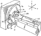
ここで図1を参照すると、本発明の一実施形態による可撓性検出器アレイ伝送回路12を用いたマルチスライスCTイメージング・システム10の図が示されている。イメージング・システム10は、X線源18と検出器アレイ組立体20とを含む回転する内部部分16を有するガントリ14を含む。X線源18は、X線のビームを検出器組立体20に向けて投射する。線源18及び検出器組立体20は、作動的に並進可能なテーブル22の周りを回転する。テーブル22は、ヘリカル・スキャンを実行するために、z軸に沿って、線源18と検出器組立体20との間を並進する。ビームは、患者ボア24内の内科患者23を透過後、検出器組立体20で検出され、CT画像を生成するのに用いられる投影データが生成される。
Referring now to FIG. 1, a diagram of a multi-slice CT imaging system 10 using a flexible detector
ここで図2を参照すると、本発明の一実施形態によるシステム10のブロック線図が示されている。線源18及び検出器組立体20は、中心軸30を中心として回転する。ビーム32は、複数の検出器素子34により受信される。各検出器素子34は、入射X線ビーム32の強度に対応する電気信号又はX線信号を生成し、バックライト・ダイオードの形態もしくは当該技術分野で公知の別の形態とすることができる。ビーム32が患者23を透過する際に、ビーム32が減弱される。ガントリの中央部分の回転、及び線源18の動作は、制御機構36により管理される。制御機構36は、線源18に電力及びタイミング信号を供給するX線制御装置38と、ガントリの中央部分の回転速度及び位置を制御するガントリ・モータ制御装置40とを含む。データ収集システム(DAS)42は、可撓性伝送回路12を介して、検出器素子34からのアナログ・データをサンプリングし、後続の処理のために、アナログ・データをデジタル信号に変換する。画像再構成装置44は、DAS42からサンプリング及びデジタル化されたX線データを受信し、高速画像再構成を実行する。主制御装置46は、CT画像を大容量記憶装置48内に格納する。
Referring now to FIG. 2, a block diagram of the system 10 according to one embodiment of the present invention is shown. The
主制御装置46は更に、オペレータ・コンソール50を介して、オペレータから指令及び走査パラメータを受信する。ディスプレイ52により、オペレータは、主制御装置46からの再構成画像及び他のデータを観察することができる。オペレータが供給した指令及びパラメータは、主制御装置46により、DAS42、X線制御装置38、及びガントリ・モータ制御装置40の操作に用いられる。更に、主制御装置46は、テーブルモータ制御装置54を操作してテーブル22を並進させ、患者12をガントリ14内に位置付ける。
The
X線制御装置38、ガントリ・モータ制御装置40、画像再構成装置44、主制御装置46、及びテーブルモータ制御装置54は、中央演算処理装置、メモリ(RAM及び/又はROM)、及び関連する入力バス及び出力バスを有するコンピュータなどのマイクロプロセッサベースであるのが好ましい。X線制御装置38、ガントリ・モータ制御装置40、画像再構成装置44、主制御装置46、及びテーブルモータ制御装置54は、中央制御装置の一部としてもよく、又は、図に示すように、各々を独立型構成要素としてもよい。
X-ray controller 38, gantry motor controller 40,
ここで図3を参照すると、本発明の一実施形態による検出器組立体20が示されている。検出器組立体は、一対のレール60と、一連の可撓性伝送回路12(説明を簡単にするために1つのみを示しているが)とを含む。各可撓性伝送回路12は、穴62を貫通して延びる留め具(図示せず)によりレール60に結合されている。コリメータ64が、散乱X線を除去して受信されたX線をシンチレータ66に集束し、シンチレータ66が、受信したX線を光エネルギに変換する。図2における検出器34のうちの1つのような検出器68が、光エネルギを受け取ってX線信号を生成し、X線信号は、1つ又はそれ以上の導電性基板層70及び可撓性回路ケーブル72を通って伝送される。可撓性回路ケーブル72は、基板層70に結合されている。一対のスペーサ・ブロック74が、レール60と基板層70との間に結合され、シンチレータ66に当接し且つ隣接するような外形にされている。一対のフレックス・クランプ/リテイナ76が、可撓性回路ケーブル72を保持し、張力を緩和する。可撓性伝送回路12及びそこに含まれる構成要素を以下に更に詳細に説明する。
Referring now to FIG. 3, a
図3の実施形態において、各可撓性回路ケーブル72は、図4において最もよく分かる複数の可撓性回路層77を有することができる。回路ケーブル72は、可撓性伝送回路12の左側78及び右側79へ向かって、フレックス・クランプ76を通り且つその上に折り重なって誘導され、「T」字形の構成を形成する。回路ケーブル72は、フレックス・クランプ76と基板層70との間にある。もちろん、当該技術分野で公知の他の構成を用いてもよい。
In the embodiment of FIG. 3, each
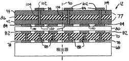
ここで図4及び図5を参照すると、本発明の一実施形態による可撓性伝送回路12の断面図及び平面図が示されている。可撓性伝送回路12は、検出器結合パッド78を介して検出器34に電気的に結合された基板層70を含む。基板層70は、以下に述べる多くの目的に役立つ。1つ又はそれ以上の単一指向性導電層80(1つのみを示す)が、基板結合パッド82を介して基板層70に電気的に結合され、基板層70と可撓性回路層77との間に単一指向性の電気的結合を形成する。可撓性回路層77は、可撓性回路結合パッド84を介して、単一指向性層80に電気的に結合され、生成されたX線信号を検出器68からデータ収集システム42へ配向する。可撓性回路層77は、可撓性回路層77間に配置された1つ又はそれ以上の絶縁層86(1つのみを示す)により互いに結合され且つ絶縁されている。
4 and 5, there are shown a cross-sectional view and a plan view of the
特定数の基板層70、単一指向性層80、可撓性回路層77、及び絶縁層86が図3〜図5に示されているが、任意の数の各層を用いることができる。
Although a particular number of substrate layers 70,
基板層70は、検出器68と可撓性回路層77との間の電気接続部の整合及び結合に対する平坦で剛直の支持体を与える。剛直状態の基板層70は、CTシステム10内に加えられる回転力に耐えることができ、検出器68及びシンチレータ66をレール60に整合させる装置を提供する。基板層70は、検出器結合パッド78と基板結合パッド82との間の電気的接続の直接ルーティング用の電気バイア88の第1のセットを提供する。電気バイア88とは、当該技術分野で知られているように、エッチング又はドリルにより層内に穴を形成し、次いで該穴を導電性材料で充填したものを指す。基板層70は、種々の電気ルーティング・パターンを形成することができ、これによりルーティング設計のみならず、可撓性伝送回路設計にも柔軟性をもたらす。
基板層70は、セラミック、有機エポキシ、プリント回路基板材料、又は、当該技術分野で公知の他の同様の基板材料を含む種々の材料で形成することができる。
単一指向性層80は、単一の軸90に沿って、基板結合パッド82と可撓性回路結合パッド84との間に、直接的電気接触を形成する。単一指向性層80は、当該技術分野で知られているように、1つ又はそれ以上の異方性のデバイスを含むことができる。異方性デバイスは、異方性導電樹脂フィルム、異方性導電樹脂メンブレインの形態とするか、又は、当該技術分野で公知の同様の形態とすることができる。
本発明の一実施形態により示される可撓性回路層77は、第1の可撓性回路層92と、第2の可撓性回路層94とを含むことができる。可撓性回路層92及び94は、検出器68からDAS42へX線信号を伝送する、並列の複数の導電性の信号線96又は信号接続部を含む。図示の実施形態において、導電線96は、可撓性回路層77の各々の間に分割されており、これにより各可撓性回路層77内に存在する導電線がより少なくなっている。所望量の電気性能を提供するのに十分なピッチを維持しながら、決められた量の検出器アレイ領域98に対し、所与の数の導電線を該領域に結合することができる。本発明は、信号線の数を可撓性回路層77間に分割することにより、1つの可撓性回路層77当たりの信号線の数を増やすことが可能となり、同時に、先行技術の可撓性伝送回路を上回るピッチの増大が得られ、従って電気性能の向上をもたらす。
The
当該技術分野で知られているように、高密度の微細な信号線を提供することとは対照的に、所与の領域内に高密度の結合パッドを形成することは比較的容易である。この理由により、及び複数の可撓性回路層の使用により、本発明は、検出器組立体20とDAS42との間の増大したX線信号の並列伝送に対する関連する信号線と共に、決められた領域内で作動結合パッドの数を増やすことができる。
As is known in the art, it is relatively easy to form a high density bond pad within a given area as opposed to providing a high density fine signal line. For this reason, and through the use of multiple flexible circuit layers, the present invention provides a defined area with associated signal lines for parallel transmission of increased X-ray signals between
第1のセットの可撓性回路結合パッド100は、第2のセットの電気バイア104を使用することにより、第2のセットの可撓性回路結合パッド102に結合されている。電気バイア104が、可撓性回路層77及び絶縁層86を通して形成されており、線96の分割されたそれぞれの部分を、第1の可撓性回路結合パッド100の指定されたそれぞれの部分に結合されている。線96は、第2の可撓性回路層94に結合されている。
The first set of flexible
第1のセットの可撓性回路結合パッド100は、単一指向性層80を通じて基板回路結合パッド82に電気的に結合されている。基板層70を用いない用途においては、可撓性回路結合パッド100は、単一指向性層80を通じ、且つ直接的に検出器結合パッド78に結合される。
The first set of flexible
可撓性回路層77は、可撓性回路ケーブル72(1つのみ図5に示す)内で結合される。可撓性回路ケーブル72及び可撓性回路層77は、図示のように単一のユニットとして一体的に形成してもよく、又は、間に結合された別個のデバイスとしてもよい。可撓性回路層77は、銅、銀、及びニッケル、並びに当該技術分野で公知の他の導電性材料を含む種々の材料で形成することができる。
The
絶縁層86は、可撓性回路層72間を分離及び絶縁する。絶縁層86は、ポリイミド層の形態とすることができ、熱可塑性樹脂、セラミック、及び当該技術分野で公知の他の絶縁材料などの材料を含むことができる。熱可塑性樹脂は、ポリエーテルイミド(PEI)、ポリエーテルエーテルケトン(PEEK)、ポリエチレンナフタレート(PEN)、ポリエチレンテレフタレート(PET)、又は当該技術分野で公知の他の同様の樹脂材料を含むことができる。 The insulating layer 86 separates and insulates between the flexible circuit layers 72. Insulating layer 86 can be in the form of a polyimide layer and can include materials such as thermoplastics, ceramics, and other insulating materials known in the art. The thermoplastic resin may include polyetherimide (PEI), polyetheretherketone (PEEK), polyethylene naphthalate (PEN), polyethylene terephthalate (PET), or other similar resin materials known in the art. it can.
線96は、絶縁層86の一体部分とするか又は絶縁層86の材料と同様の材料で形成することができる絶縁材料97により分離される。絶縁材料はまた、接着性材料を含むことができ、線96の配列と、可撓性回路層77及び可撓性回路ケーブル72の形状とを維持するのを支援し、並びにこれらの使用の耐久性を付与することができる。
Lines 96 are separated by an insulating material 97 that can be an integral part of insulating layer 86 or formed of a material similar to that of insulating layer 86. The insulating material can also include an adhesive material to help maintain the alignment of the wires 96 and the shape of the
検出器結合パッド78、基板結合パッド82、及び可撓性回路結合パッド84は、導電性パッドの形態とすることができ、従って、当該技術分野で公知の種々の導電性材料で形成することができる。図5において、可撓性回路結合パッドは、1つおきの結合パッドが第1の可撓性回路結合パッド100のうちの1つであって、第1の可撓性回路層92に対応し、残りの結合パッドの各々が第2の可撓性回路層94に対応する第2の可撓性回路結合パッド102のうちの1つであるような、交互配列で示されている。任意の数の可撓性回路結合パッド84の横列及び縦列が存在することができる。
The
可撓性伝送回路12は、当該技術分野で公知の熱技術及び圧力技術を用いて形成することができる。可撓性伝送回路12はまた、可撓性回路層77の接着結合により形成してもよい。
The
ここで図6を参照すると、本発明の一実施形態によるマルチスライスCTイメージング・システム10に対する画像再構成法を示す論理フロー図が示されている。 Referring now to FIG. 6, a logic flow diagram illustrating an image reconstruction method for a multi-slice CT imaging system 10 according to one embodiment of the present invention is shown.
ステップ120で、線源18が、X線ビーム32を発生する。ステップ122で、検出器組立体20が、患者23のヘリカル・スキャンを実行し、X線ビーム32を受信し、X線信号の形態の投影データを生成する。
In
ステップ124で、基板層70が、第1のセットのバイア88を通じて、X線信号を、単一指向性層80へルーティング及び転送する。ステップ126で、単一指向性層80が、X線信号を、基板層70から可撓性回路層77へ、一方向に転送する。ステップ128で、可撓性回路層が、X線信号を、単一指向性層80からDAS42へルーティングする。ステップ130で、X線信号に応答して画像が再構成される。
At
上述のステップは、例証となる実施例であることを意味し、各ステップは、用途に応じて、同期して、連続して、同時に、又は異なる順序で実行することができる。 The above steps are meant to be illustrative examples, and each step can be performed synchronously, sequentially, simultaneously, or in a different order, depending on the application.
本発明は、複数の可撓性回路層及び基板層を有する可撓性検出器アレイ伝送回路を提供する。本発明は、複数の可撓性回路層を用いることにより、可撓性回路層内の信号線間のピッチを増大し、歩留まりを高め、電気性能を向上させる。本発明は、基板層を用いることにより、ルーティング・パターンの柔軟性をも向上させることができる。 The present invention provides a flexible detector array transmission circuit having a plurality of flexible circuit layers and a substrate layer. The present invention uses a plurality of flexible circuit layers to increase the pitch between signal lines in the flexible circuit layer, increase the yield, and improve the electrical performance. The present invention can also improve the flexibility of the routing pattern by using the substrate layer.
本発明を、1つ又はそれ以上の実施形態に関して説明してきたが、説明してきた特定の機構及び技法は本発明の原理の単なる例証であり、添付の特許請求の範囲によって定義される本発明の精神及び範囲から逸脱することなく、多くの修正を、説明した本方法及び装置に対して行うことができることを理解すべきである。 Although the invention has been described in terms of one or more embodiments, the specific mechanisms and techniques described are merely illustrative of the principles of the invention and are defined by the scope of the invention as defined by the appended claims. It should be understood that many modifications can be made to the described method and apparatus without departing from the spirit and scope.
120 X線ビームを発生する
122 X線信号を生成する
124 X線信号を、基板層を介して検出器から単一指向性層へ転送する
126 X線信号を、基板層から可撓性回路層へ、一方向に転送する
128 X線信号を、可撓性回路層を通してデータ収集システムへルーティングする
130 X線信号に応答して画像を再構成する
120 Generate
Claims (8)
前記少なくとも1つの単一指向性導電層80に電気的に結合される複数の可撓性回路層77と、
前記複数の可撓性回路層77間に配置された少なくとも1つの絶縁層86と、
を備え、
前記複数の可撓性回路層77の各層が、前記少なくとも1つの検出器68により生成されたX線信号をデータ収集システム42へ配向する、X線イメージング・システム10用の可撓性検出器アレイ伝送回路12。 At least one unidirectional conductive layer 80 electrically coupled to at least one detector 68;
A plurality of flexible circuit layers 77 electrically coupled to the at least one unidirectional conductive layer 80;
At least one insulating layer 86 disposed between the plurality of flexible circuit layers 77;
With
A flexible detector array for the X-ray imaging system 10, wherein each layer of the plurality of flexible circuit layers 77 directs the X-ray signal generated by the at least one detector 68 to the data acquisition system 42. Transmission circuit 12;
前記X線ビーム32を受信して投影データを生成する少なくとも1つの検出器68と、
可撓性検出器アレイ伝送回路12と、
を備えるX線イメージング・システム10であって、
前記可撓性検出器アレイ伝送回路12が、前記少なくとも1つの検出器68に複数のパッドを介して電気的に結合された少なくとも1つの単一指向性導電層80と、前記少なくとも1つの単一指向性導電層80に電気的に結合された複数の可撓性回路層77と、前記複数の可撓性回路層77間に配置された少なくとも1つの絶縁層86とを含み、
前記X線イメージング・システム10が更に、
前記可撓性検出器アレイ伝送回路12に電気的に結合された、前記少なくとも1つの検出器68から前記投影データを受信して前記投影データに応答して画像を再構成する画像再構成装置44と、
を備えるシステム。 A source 18 for generating an X-ray beam 32;
At least one detector 68 that receives the x-ray beam 32 and generates projection data;
A flexible detector array transmission circuit 12;
An X-ray imaging system 10 comprising:
The flexible detector array transmission circuit 12 includes at least one unidirectional conductive layer 80 electrically coupled to the at least one detector 68 via a plurality of pads; and the at least one single A plurality of flexible circuit layers 77 electrically coupled to the directional conductive layer 80; and at least one insulating layer 86 disposed between the plurality of flexible circuit layers 77;
The X-ray imaging system 10 further includes:
An image reconstruction device 44, which is electrically coupled to the flexible detector array transmission circuit 12, receives the projection data from the at least one detector 68 and reconstructs an image in response to the projection data. When,
A system comprising:
The system of claim 6 , further comprising at least one conductive substrate layer 70 electrically coupled to the at least one detector 68 and the at least one unidirectional conductive layer 80.
Applications Claiming Priority (1)
| Application Number | Priority Date | Filing Date | Title |
|---|---|---|---|
| US10/604,449 US7010088B2 (en) | 2003-07-22 | 2003-07-22 | Multi-slice CT multi-layer flexible signal transmission detector circuit |
Publications (3)
| Publication Number | Publication Date |
|---|---|
| JP2005040610A JP2005040610A (en) | 2005-02-17 |
| JP2005040610A5 JP2005040610A5 (en) | 2009-10-22 |
| JP4502736B2 true JP4502736B2 (en) | 2010-07-14 |
Family
ID=34062266
Family Applications (1)
| Application Number | Title | Priority Date | Filing Date |
|---|---|---|---|
| JP2004212468A Expired - Fee Related JP4502736B2 (en) | 2003-07-22 | 2004-07-21 | Multi-layer flexible signal transmission detector circuit for multi-slice CT |
Country Status (4)
| Country | Link |
|---|---|
| US (1) | US7010088B2 (en) |
| JP (1) | JP4502736B2 (en) |
| DE (1) | DE102004035405A1 (en) |
| IL (1) | IL162905A (en) |
Families Citing this family (15)
| Publication number | Priority date | Publication date | Assignee | Title |
|---|---|---|---|---|
| WO2007039840A2 (en) * | 2005-10-05 | 2007-04-12 | Koninklijke Philips Electronics, N.V. | Computed tomography detector using thin circuits |
| US7455454B2 (en) * | 2006-10-03 | 2008-11-25 | General Electric Company | X-ray detector methods and apparatus |
| JP5503883B2 (en) * | 2009-03-06 | 2014-05-28 | 株式会社東芝 | X-ray CT apparatus and X-ray detection apparatus |
| WO2010122433A2 (en) * | 2009-04-22 | 2010-10-28 | Koninklijke Philips Electronics N.V. | Imaging measurement system with a printed organic photodiode array |
| WO2011030240A2 (en) * | 2009-09-08 | 2011-03-17 | Koninklijke Philips Electronics N.V. | Imaging measurement system with a printed photodetector array |
| JP5436121B2 (en) * | 2009-09-28 | 2014-03-05 | キヤノン株式会社 | Imaging apparatus and radiation imaging system |
| US8610079B2 (en) * | 2009-12-28 | 2013-12-17 | General Electric Company | Robust radiation detector and method of forming the same |
| CN104067146A (en) * | 2011-12-27 | 2014-09-24 | 皇家飞利浦有限公司 | Flexible connectors for pet detectors |
| WO2013176657A1 (en) * | 2012-05-22 | 2013-11-28 | Analogic Corporaton | Detection system and detector array interconnect assemblies |
| US9788804B2 (en) * | 2014-07-22 | 2017-10-17 | Samsung Electronics Co., Ltd. | Anatomical imaging system with improved detector block module |
| US9603574B2 (en) | 2014-12-17 | 2017-03-28 | General Electric Company | Reconfigurable electronic substrate |
| DE102014226985B4 (en) * | 2014-12-23 | 2024-02-08 | Carl Zeiss Microscopy Gmbh | Method for analyzing an object, computer program product and particle beam device for carrying out the method |
| US10764361B2 (en) * | 2015-12-28 | 2020-09-01 | Netsapiens, Inc. | Distributed server architecture session count system and methods |
| JP7166833B2 (en) * | 2018-08-03 | 2022-11-08 | キヤノンメディカルシステムズ株式会社 | Radiation detector and radiation detector module |
| CN114886453A (en) * | 2022-07-12 | 2022-08-12 | 芯晟捷创光电科技(常州)有限公司 | CT detection module based on front-illuminated photodiode array and corresponding CT machine |
Citations (3)
| Publication number | Priority date | Publication date | Assignee | Title |
|---|---|---|---|---|
| JP2001318155A (en) * | 2000-02-28 | 2001-11-16 | Toshiba Corp | Radiation detector and x-ray ct device |
| JP2002257936A (en) * | 2001-03-02 | 2002-09-11 | Hamamatsu Photonics Kk | Radiation detection module |
| US6475824B1 (en) * | 1998-10-07 | 2002-11-05 | Lg. Philips Lcd Co., Ltd. | X-ray detector and method of fabricating the same |
Family Cites Families (3)
| Publication number | Priority date | Publication date | Assignee | Title |
|---|---|---|---|---|
| US6343171B1 (en) | 1998-10-09 | 2002-01-29 | Fujitsu Limited | Systems based on opto-electronic substrates with electrical and optical interconnections and methods for making |
| US6299713B1 (en) | 1999-07-15 | 2001-10-09 | L. M. Bejtlich And Associates, Llc | Optical radiation conducting zones and associated bonding and alignment systems |
| US6859514B2 (en) * | 2003-03-14 | 2005-02-22 | Ge Medical Systems Global Technology Company Llc | CT detector array with uniform cross-talk |
-
2003
- 2003-07-22 US US10/604,449 patent/US7010088B2/en not_active Expired - Lifetime
-
2004
- 2004-07-07 IL IL162905A patent/IL162905A/en unknown
- 2004-07-21 JP JP2004212468A patent/JP4502736B2/en not_active Expired - Fee Related
- 2004-07-21 DE DE102004035405A patent/DE102004035405A1/en not_active Withdrawn
Patent Citations (3)
| Publication number | Priority date | Publication date | Assignee | Title |
|---|---|---|---|---|
| US6475824B1 (en) * | 1998-10-07 | 2002-11-05 | Lg. Philips Lcd Co., Ltd. | X-ray detector and method of fabricating the same |
| JP2001318155A (en) * | 2000-02-28 | 2001-11-16 | Toshiba Corp | Radiation detector and x-ray ct device |
| JP2002257936A (en) * | 2001-03-02 | 2002-09-11 | Hamamatsu Photonics Kk | Radiation detection module |
Also Published As
| Publication number | Publication date |
|---|---|
| DE102004035405A1 (en) | 2005-02-10 |
| IL162905A (en) | 2009-07-20 |
| JP2005040610A (en) | 2005-02-17 |
| US7010088B2 (en) | 2006-03-07 |
| IL162905A0 (en) | 2005-11-20 |
| US20050018810A1 (en) | 2005-01-27 |
Similar Documents
| Publication | Publication Date | Title |
|---|---|---|
| JP4502736B2 (en) | Multi-layer flexible signal transmission detector circuit for multi-slice CT | |
| US6115448A (en) | Photodiode array for a scalable multislice scanning computed tomography system | |
| JP5432448B2 (en) | Computerized tomography detector module configuration | |
| JP5951261B2 (en) | Multi-slice CT detector with tileable packaging structure | |
| JP5455620B2 (en) | Radiation detector and apparatus including the detector | |
| US7379528B2 (en) | Radiation detector with shielded electronics for computed tomography | |
| JP2008286800A (en) | Radiation detector, radiation detection system, and x-ray ct apparatus having radiation detector | |
| US20080253507A1 (en) | Computed Tomography Detector Using Thin Circuits | |
| EP1355382A2 (en) | High density flex interconnect for CT detectors | |
| JP2001318155A (en) | Radiation detector and x-ray ct device | |
| JP2007078369A (en) | Radiation ray detection module, printed substrate and positron emission tomography apparatus | |
| US10488531B2 (en) | Detection system and detector array interconnect assemblies | |
| US20060256922A1 (en) | X-ray CT apparatus | |
| JP4512851B2 (en) | X-ray beam detector module, flexible electrical cable, mounting bracket and method of manufacturing the same | |
| JP4564141B2 (en) | X-ray CT system | |
| JP2008122116A (en) | Radiation detector and x-ray tomography | |
| JP4831300B2 (en) | Multi-die back-illuminated diode module assembly | |
| EP2367028B1 (en) | Radioactive ray detecting apparatus, method of manufacturing the same, and imaging system | |
| JP4341088B2 (en) | Elastomer connection for computed tomography systems | |
| US6235993B1 (en) | Cable for computed tomography system | |
| JP2016035449A (en) | X-ray computer tomography apparatus and x-ray detector | |
| US20220323028A1 (en) | Packaging for ct scanner for spectral imaging | |
| CN115462821A (en) | CT detector module | |
| JP2006116342A (en) | X-ray ct system |
Legal Events
| Date | Code | Title | Description |
|---|---|---|---|
| A521 | Request for written amendment filed |
Free format text: JAPANESE INTERMEDIATE CODE: A523 Effective date: 20070719 |
|
| A621 | Written request for application examination |
Free format text: JAPANESE INTERMEDIATE CODE: A621 Effective date: 20070719 |
|
| A521 | Request for written amendment filed |
Free format text: JAPANESE INTERMEDIATE CODE: A523 Effective date: 20090908 |
|
| RD02 | Notification of acceptance of power of attorney |
Free format text: JAPANESE INTERMEDIATE CODE: A7422 Effective date: 20090908 |
|
| RD04 | Notification of resignation of power of attorney |
Free format text: JAPANESE INTERMEDIATE CODE: A7424 Effective date: 20090908 |
|
| A131 | Notification of reasons for refusal |
Free format text: JAPANESE INTERMEDIATE CODE: A131 Effective date: 20090915 |
|
| A521 | Request for written amendment filed |
Free format text: JAPANESE INTERMEDIATE CODE: A523 Effective date: 20091029 |
|
| A131 | Notification of reasons for refusal |
Free format text: JAPANESE INTERMEDIATE CODE: A131 Effective date: 20100105 |
|
| A521 | Request for written amendment filed |
Free format text: JAPANESE INTERMEDIATE CODE: A523 Effective date: 20100303 |
|
| TRDD | Decision of grant or rejection written | ||
| A01 | Written decision to grant a patent or to grant a registration (utility model) |
Free format text: JAPANESE INTERMEDIATE CODE: A01 Effective date: 20100330 |
|
| A01 | Written decision to grant a patent or to grant a registration (utility model) |
Free format text: JAPANESE INTERMEDIATE CODE: A01 |
|
| A61 | First payment of annual fees (during grant procedure) |
Free format text: JAPANESE INTERMEDIATE CODE: A61 Effective date: 20100420 |
|
| R150 | Certificate of patent or registration of utility model |
Ref document number: 4502736 Country of ref document: JP Free format text: JAPANESE INTERMEDIATE CODE: R150 Free format text: JAPANESE INTERMEDIATE CODE: R150 |
|
| FPAY | Renewal fee payment (event date is renewal date of database) |
Free format text: PAYMENT UNTIL: 20130430 Year of fee payment: 3 |
|
| FPAY | Renewal fee payment (event date is renewal date of database) |
Free format text: PAYMENT UNTIL: 20130430 Year of fee payment: 3 |
|
| FPAY | Renewal fee payment (event date is renewal date of database) |
Free format text: PAYMENT UNTIL: 20140430 Year of fee payment: 4 |
|
| R250 | Receipt of annual fees |
Free format text: JAPANESE INTERMEDIATE CODE: R250 |
|
| R250 | Receipt of annual fees |
Free format text: JAPANESE INTERMEDIATE CODE: R250 |
|
| R250 | Receipt of annual fees |
Free format text: JAPANESE INTERMEDIATE CODE: R250 |
|
| R250 | Receipt of annual fees |
Free format text: JAPANESE INTERMEDIATE CODE: R250 |
|
| R250 | Receipt of annual fees |
Free format text: JAPANESE INTERMEDIATE CODE: R250 |
|
| R250 | Receipt of annual fees |
Free format text: JAPANESE INTERMEDIATE CODE: R250 |
|
| R250 | Receipt of annual fees |
Free format text: JAPANESE INTERMEDIATE CODE: R250 |
|
| R250 | Receipt of annual fees |
Free format text: JAPANESE INTERMEDIATE CODE: R250 |
|
| LAPS | Cancellation because of no payment of annual fees |