JP4475692B2 - Bus signal noise reduction method - Google Patents
Bus signal noise reduction method Download PDFInfo
- Publication number
- JP4475692B2 JP4475692B2 JP23984598A JP23984598A JP4475692B2 JP 4475692 B2 JP4475692 B2 JP 4475692B2 JP 23984598 A JP23984598 A JP 23984598A JP 23984598 A JP23984598 A JP 23984598A JP 4475692 B2 JP4475692 B2 JP 4475692B2
- Authority
- JP
- Japan
- Prior art keywords
- bus
- impedance
- signal
- output
- clamping device
- Prior art date
- Legal status (The legal status is an assumption and is not a legal conclusion. Google has not performed a legal analysis and makes no representation as to the accuracy of the status listed.)
- Expired - Fee Related
Links
Images

Classifications
-
- H—ELECTRICITY
- H03—ELECTRONIC CIRCUITRY
- H03K—PULSE TECHNIQUE
- H03K5/00—Manipulating of pulses not covered by one of the other main groups of this subclass
- H03K5/125—Discriminating pulses
- H03K5/1252—Suppression or limitation of noise or interference
-
- H—ELECTRICITY
- H04—ELECTRIC COMMUNICATION TECHNIQUE
- H04L—TRANSMISSION OF DIGITAL INFORMATION, e.g. TELEGRAPHIC COMMUNICATION
- H04L25/00—Baseband systems
- H04L25/02—Details ; arrangements for supplying electrical power along data transmission lines
Description
【0001】
【発明の属する技術分野】
本発明は、電子回路に関するものである。本発明は特に、集積回路の入力/出力回路に関するものである。さらに詳細に言えば、本発明はいくつかの集積回路間において相互接続された高速信号のオーバシュート及びアンダーシュートを低減するための回路に関するものである。
【0002】
【従来の技術】
複数の集積回路の全てが共通信号に接続される場合が多い。この1つの例として、複数のDRAMチップに接続されたマイクロプロセッサにおけるデータ・ラインがある。プリント回路基板のレイアウトを単純化するために、これらのチップの全てを接続するトレースを主トランク・ラインとして経路指定し、小さい「スタブ」を該トランクから分岐させて、これに各個別のデバイスを接続することが可能である。これは、バスと呼ばれることが多い。この構成は便利ではあるが、厳しいグリッチ及び信号の完全性の問題が生じる可能性がある。これは特に、信号の立ち上がりまたは立ち下がり時間が、スタブを伝わる信号の伝搬時間より短い場合に当てはまる。信号の完全性の問題が生じるのは、高速の立ち上がりまたは立ち下がり信号がスタブの端部の開回路インピーダンスにより反射され、スタブに沿って伝搬し、トランク・ラインに戻される場合である。これらの反射は、バスの全ての位置において動的に所望の信号電圧に加えられるか、あるいは所望の信号電圧から減じられるので、グリッチが生じ、セトリング時間が長くなる可能性がある。
【0003】
【発明が解決しようとする課題】
従って、本発明の目的は、バス全体の速度が遅くなる原因となる信号の立ち上がりまたは立ち下がりの低速化を誘発することなく、さらに、バスのノイズ・イミュニティが低下する原因となるバスにおける電圧のスイングの縮小化をもたらすことのない、バス・スタブにおける反射を低減する改良された方法を提供することにある。
【0004】
【課題を解決するための手段】
本発明は、バスにおいてローからハイへの遷移またはハイからローへの遷移が生じると、これを検知することによって、各バス毎の反射を低減させる。遷移を検出すると、短い時間期間にわたって信号を新規(遷移後)電圧にクランプする、インピーダンス整合されたクランプ装置が起動する。このクランプ作用によって、反射波のエネルギが減少し、バスの電圧を変化させる反射波の影響が低下する。バス・スタブの端部における各非駆動装置がこのクランプ作用を実施する。これによって、信号の完全性に及ぼされる全てのスタブの影響が最小限に抑えられる。
【0005】
【実施例】
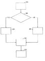
図2には、反射波のエネルギを低減させるために実施されるステップが示されている。以下にその内容を列記する。
202:まず、バスに遷移が生じると、スタブの端部に接続された装置がそれを検出する。
204:前記装置は、ハイからローへの遷移であるか、または、ローからハイへの遷移であるかを判定する。
206:ハイからローへの遷移であれば、前記装置は、第1のインピーダンスを介してバスをロー論理レベルにクランプするクランプ装置をオンにする。
208:ローからハイへの遷移であれば、前記装置は、第2のインピーダンスを介してバスをハイ論理レベルにクランプするクランプ装置をオンにする。
210:その後、前記装置は、それぞれのクランプ装置をオン状態にする時間期間だけ待機する。
212:その時間期間が経過すると、オンにされていたクランプ装置がオフにされる。
【0006】
図1は、図2のステップを実施する回路の概略図である。パッド102は、バスに電気的に接続されている。ドライバ104は、バスの駆動が可能な装置に設けられているであろう任意の出力ドライバである。ドライバ104の出力は、バスを駆動するためにパッド102に接続される。
【0007】
その入力がパッド102に接続された受信器106は、バスの論理レベルを検知する。受信器106の出力は、ボックス150内に示されたパルス発生器回路に接続されている。パルス発生器回路150は、受信器106の出力変化に応答し、2つの出力CHまたはCLの一方からパルスを送り出す。受信器106の出力が、バスにロー論理レベルからハイ論理レベルへの遷移が生じたことを表している場合、パルス発生器回路150はCH出力にパルスを送り出す。受信器106の出力がバスにハイ論理レベルからロー論理レベルへの遷移が生じたことを表している場合、パルス発生器回路150はCL出力にパルスを送り出す。
【0008】
望ましい実施態様の場合、受信器106の出力は、NANDゲート108の第1の入力、NORゲート110の第1の入力、及び、遅延装置112の入力に接続される。遅延装置112の出力はインバータ128の入力に接続される。インバータ128の出力はNANDゲート108の第2の入力及びNORゲート110の第2の入力に接続される。NANDゲート108の出力はノードCHである。NORゲート110の出力はノードCLである。NANDゲート108の出力、すなわちノードCHは、pチャネル電界効果トランジスタ(PFET)114のゲートに接続される。PFET114のドレインはハイ論理レベルを画定する電源に接続される。図1の場合、これは正電源VDDである。PFET114のソースは、パッド102に接続される。パッド102に接続されたバス・スタブにおける反射を最小限に抑えるために、PFET114の寸法は、PFET114がオンになったときのそのインピーダンスがパッド102に接続されたバス・スタブのインピーダンスに近似するように選択するのが望ましい。
【0009】
遅延装置112は、いくつかの方法で構成することが可能である。遅延装置の入力と出力の間に接続された抵抗器と、その出力から負電源GNDに接続されたコンデンサから構成されるRCネットワークを利用することが可能である。直列に接続された複数のインバータを利用することも可能である。これらのインバータは、インバータの速度を調整して、プロセス、電圧、及び温度の変動を補償する補償回路に接続することが可能である。駆動の競合を回避するために、遅延装置がもたらす遅延量は、バスのサイクル時間より短くすべきである。
【0010】
NORゲート110の出力、すなわちノードCLは、2つのnチャネル電界効果トランジスタ(NFET)116及び118のゲートに接続される。NFET116のドレインは正の電源電圧VDDに接続される。NFET116のソースはパッド102に接続される。NFET118のドレインは、パッド102に接続される。NFET118のソースはアースに接続される。
【0011】
NFET116及び118を直列に接続すると、該NFETが両方ともオンになると、パッドの電圧をセットする抵抗分割器が形成される。この抵抗分割器は、バスをプログラマブル電圧レベルにクランプする働きをし、クランプ電圧が、負の電源電圧ではない、バスのロー論理レベルを画定する電圧に整合できるようにする。バスのロー論理レベルを画定する電圧が負の電源電圧に等しい場合は、抵抗分割器を単一トランジスタに置き換えることも可能である。パッド102に接続されたバス・スタブにおける反射を最小限に抑えるため、NFET116及び118の寸法は、NFET116及び118がオンになった時の、その並列インピーダンスが、パッド102に接続されたバス・スタブのインピーダンスに近似するように選択することが望ましい。当該技術者には明らかなように、NFET116及び118から構成される抵抗分割器のテブナンの等価回路は、バスのロー論理レベルに等しい電圧源と、並列をなすNFET116及び118のインピーダンスになる。同様に、当該技術者には明らかなように、バスにおけるハイ論理レベルを画定する電圧が、正の電源電圧でなければ、2つのPFETから構成される電圧分割器の代わりにPFET114を用いて、バスにおけるハイ論理レベルに等しい電圧源と、第2のインピーダンスから構成されるテブナンの等価回路を形成することも可能である。
【0012】
CLが切換わる時にNFET116及び118のゲート・キャパシタンスによってバスに放出される電荷を補償するようにするのも望ましい。この補償は、インバータ120及びコンデンサ122によって実施することが可能である。インバータ120に対する入力はノードCLに接続される。インバータ120の出力はコンデンサ122の端子の1つに接続される。コンデンサ122のもう1つの端子はパッド102に接続される。ノードCLが切換わると、インバータ120の出力はそれとは逆方向に切換わる。この結果、コンデンサ122は、NFET116及び118のゲート・キャパシタンスによってパッド102に付加される電荷またはパッド102から除去される電荷とは逆になるように、パッド102に電荷を付加するか、または、パッド102から電荷を除去する。こうして、パッド102、ひいてはバスに放出される電荷の少なくとも一部は、インバータ120及びコンデンサ122によって補償される。同様に、CHが切換わるときにPFET114のゲート・コンデンサによってバスに放出される電荷を補償することが望ましい場合もある。これは、その入力がCH及びもう1つのコンデンサに接続されたインバータによって実施可能である。
【0013】
もちろん、請求の範囲に記載の発明は、望ましい実施態様によって限定されるべきものではなく、本発明の概念の範囲及び精神の内に他の修正及び変更を包含するものである。例えば、本発明の説明は、複数のスタブを備えたバスにおける信号のクランプに関連して行われてきた。しかし、ある2点間を結ぶ、スタブのない信号ラインにおいても容易に利用することが可能である。解説した実施態様は、例証のためのものとみなすべきであって、限定とみなすべきではなく、本発明の範囲は、以上の説明よってではなく、特許請求の範囲によって明らかにされている。
【0014】
〔実施態様〕
なお、本発明の実施態様の例を以下に示す。
【0015】
〔実施態様1〕 信号のノイズを低減する方法であって、
(a)第1の電圧レベルから第2の電圧レベルへの信号の遷移を検出するステップ(202)と、
(b)前記第2の電圧レベルが第1の電圧範囲内にある場合、第1のクランプ装置をオンにするステップであって、
前記第1の電圧範囲はロー論理レベルを画定することと、
前記第1のクランプ装置は前記信号に接続されることと、
前記第1のクランプ装置は、オンになると、第1の電圧源と、前記信号と論理基準電圧の間に直列に接続された第1のインピーダンスから構成される第1のテブナンの等価回路を形成すること
を特徴とするステップ(206)と、
(c)前記第2の電圧レベルが第2の電圧範囲内にある場合、第2のクランプ装置をオンにするステップであって、
前記第2の電圧範囲はハイ論理レベルを画定することと、
前記第2のクランプ装置は前記信号に接続されることと、
前記第2のクランプ装置は、オンになると、第2の電圧源と、前記信号と論理基準電圧の間に直列に接続された第2のインピーダンスから構成される第2のテブナンの等価回路を形成すること
を特徴とするステップ(208)と、
(d)前記第1のクランプ装置と前記第2のクランプ装置の一方がオンになっている時間期間にわたって待機するステップ(210)と、
(e)オンになっている前記第1のクランプ装置と前記第2のクランプ装置の前記一方をオフにするステップ(212)と
を設けて成る方法。
【0016】
〔実施態様2〕 信号のノイズを低減するための装置であって、
受信器出力と受信器入力を備えた受信器(106)であって、前記受信器入力が前記信号に接続され、前記受信器出力が、前記信号がロー論理レベルかハイ論理レベルかを示す受信器(106)と、
パルス発生器入力、クランプ・ハイ出力(CH)、及びクランプ・ロー出力(CL)を備えたパルス発生器(150)であって、前記パルス発生器入力が前記受信器出力に結合され、前記クランプ・ハイ出力が前記パルス発生器入力に応答して、前記パルス発生器入力が前記信号がロー論理レベルからハイ論理レベルに遷移したことを示した時に、第1のパルスを発生し、さらに、前記クランプ・ロー出力が前記パルス発生器入力に応答して、前記パルス発生器入力が前記信号がハイ論理レベルからロー論理レベルに遷移したことを示した時に第2のパルスを発生するように構成されたパルス発生器(150)と、
前記クランプ・ハイ出力に結合されて、オンになると、前記信号と第1の電源ノードの間に無限でない第1のインピーダンスを生じる第1のクランプ装置(114)であって、前記第1のパルスの期間だけオンになる第1のクランプ装置(114)と、
前記クランプ低出力に結合されて、オンになると、前記信号と第2の電源ノードとの間に無限でない第2のインピーダンスを生じる第2のクランプ装置(118)であって、前記第2のパルスの期間だけオンになる第2のクランプ装置(118)と
を設けて成る装置。
【0017】
〔実施態様3〕 前記クランプ・ロー出力に結合されて、オンになると、前記信号と前記第1の電源ノードの間に無限でない第3のインピーダンスを生じ、前記第2のパルスの期間だけオンになる第3のクランプ装置(116)がさらに含まれていることを特徴とする、実施態様2に記載の装置。
【0018】
〔実施態様4〕 前記クランプ・ハイ出力に結合されて、オンになると、前記信号と前記第2の電源ノードの間に無限でない第4のインピーダンスを生じ、前記第1のパルスの間だけオンになる第4のクランプ装置がさらに含まれていることを特徴とする、実施態様2または実施態様3に記載の装置。
【0019】
〔実施態様5〕 前記パルス発生器に、遅延入力と遅延出力を備えた遅延装置(112)が含まれていることと、
前記遅延出力は、一定の時間期間遅延された後、前記遅延入力に続いて振舞うことと、
前記遅延入力が前記受信器出力に結合されること
を特徴とする、実施態様2乃至実施態様4のいずれか一項に記載の装置。
【0020】
〔実施態様6〕 前記パルス発生器に、NANDゲート(108)とNORゲート(110)が含まれることと、
前記NANDゲート(108)と前記NORゲート(110)はともに、前記受信器出力と前記遅延出力の両方に結合される入力を備えることを特徴とする、実施態様2乃至実施態様5のいずれか一項に記載の装置。
【0021】
〔実施態様7〕 前記NANDゲート(108)がNAND出力を備え、前記NORゲート(110)がNOR出力を備えることと、
前記NAND出力が前記クランプ・ハイ出力を備え、前記NOR出力が前記クランプ・ロー出力を備えることを特徴とする、実施態様6に記載の装置。
【0022】
〔実施態様8〕 前記第1のクランプ装置(114)は電界効果トランジスタであり、前記第2のクランプ装置(118)は電界効果トランジスタであることを特徴とする、実施態様2に記載の装置。
【0023】
〔実施態様9〕 前記第3のクランプ装置(116)は電界効果トランジスタであり、前記第4のクランプ装置は電界効果トランジスタであることを特徴とする、実施態様3または実施態様4に記載の装置。
【0024】
〔実施態様10〕 前記第1のクランプ装置(114)は電界効果トランジスタであり、前記第2のクランプ装置(118)は電解効果トランジスタであり、前記第3のクランプ装置(116)は電界効果トランジスタであり、前記第4のクランプ装置は電界効果トランジスタであることを特徴とする、実施態様5乃至実施態様7のいずれか一項に記載の装置。
【図面の簡単な説明】
【図1】本発明を実施する回路の概略図である。
【図2】反射波のエネルギを低減させるために、本発明によって実施されるステップを表した流れ図である。
【符号の説明】
102 パッド
104 ドライバ
106 受信器
108 NANDゲート
110 NORゲート
112 遅延装置
114 PFET
116 NFET
118 NFET
120 インバータ
122 コンデンサ
128 インバータ
150 パルス発生器[0001]
BACKGROUND OF THE INVENTION
The present invention relates to an electronic circuit. The invention particularly relates to input / output circuits of integrated circuits. More particularly, the present invention relates to a circuit for reducing overshoot and undershoot of high speed signals interconnected between several integrated circuits.
[0002]
[Prior art]
In many cases, all of a plurality of integrated circuits are connected to a common signal. One example of this is a data line in a microprocessor connected to multiple DRAM chips. To simplify the layout of the printed circuit board, the trace connecting all of these chips is routed as the main trunk line, and a small "stub" is branched from the trunk to each individual device. It is possible to connect. This is often called a bus. While this arrangement is convenient, severe glitches and signal integrity problems can arise. This is especially true when the signal rise or fall time is shorter than the signal propagation time through the stub. A signal integrity problem arises when a fast rising or falling signal is reflected by the open circuit impedance at the end of the stub, propagates along the stub, and returns to the trunk line. These reflections are dynamically added to or subtracted from the desired signal voltage at all locations on the bus, resulting in glitches and increased settling time.
[0003]
[Problems to be solved by the invention]
Accordingly, it is an object of the present invention to induce a reduction in the voltage on the bus that causes a decrease in bus noise immunity without inducing a slow rise or fall in the signal that causes the overall bus speed to slow. It is an object to provide an improved method of reducing reflections on a bus stub without causing a reduction in swing.
[0004]
[Means for Solving the Problems]
The present invention reduces reflection for each bus by detecting when a low-to-high transition or a high-to-low transition occurs on the bus. When a transition is detected, an impedance matched clamping device is activated that clamps the signal to a new (post-transition) voltage for a short period of time. By this clamping action, the energy of the reflected wave is reduced, and the influence of the reflected wave that changes the voltage of the bus is reduced. Each non-drive device at the end of the bus stub performs this clamping action. This minimizes the effect of all stubs on the signal integrity.
[0005]
【Example】
FIG. 2 shows the steps performed to reduce the energy of the reflected wave. The contents are listed below.
202: First, when a transition occurs on the bus, a device connected to the end of the stub detects it.
204: The device determines whether it is a high-to-low transition or a low-to-high transition.
206: If a transition from high to low, the device turns on a clamping device that clamps the bus to a low logic level via the first impedance.
208: If low-to-high transition, the device turns on the clamping device that clamps the bus to a high logic level via the second impedance.
210: The device then waits for a period of time to turn on the respective clamping device.
212: When the time period elapses, the clamp device that was turned on is turned off.
[0006]
FIG. 1 is a schematic diagram of a circuit that implements the steps of FIG. The
[0007]
A
[0008]
In the preferred embodiment, the output of the
[0009]
The
[0010]
The output of NOR
[0011]
Connecting
[0012]
It is also desirable to compensate for the charge released into the bus by the gate capacitance of
[0013]
Of course, the claimed invention is not to be limited by the preferred embodiments, but includes other modifications and variations within the scope and spirit of the inventive concept. For example, the present invention has been described with reference to signal clamping in a bus with multiple stubs. However, it can be easily used even in a signal line that does not have a stub and connects between two points. The described embodiments are to be regarded as illustrative and not restrictive, and the scope of the invention is defined by the appended claims rather than by the foregoing description.
[0014]
Embodiment
Examples of embodiments of the present invention are shown below.
[0015]
Embodiment 1 A method for reducing noise in a signal,
(A) detecting a signal transition from a first voltage level to a second voltage level (202);
(B) turning on the first clamping device if the second voltage level is within the first voltage range,
The first voltage range defines a low logic level;
The first clamping device is connected to the signal;
When the first clamping device is turned on, it forms an equivalent circuit of a first Thevenin consisting of a first voltage source and a first impedance connected in series between the signal and a logic reference voltage. A step (206) characterized by:
(C) turning on the second clamping device if the second voltage level is within a second voltage range,
The second voltage range defines a high logic level;
The second clamping device is connected to the signal;
When the second clamping device is turned on, it forms an equivalent circuit of a second voltage source and a second Thevenin composed of a second impedance connected in series between the signal and a logic reference voltage. A step (208) characterized by:
(D) waiting (210) for a period of time during which one of the first clamping device and the second clamping device is on;
(E) providing a step (212) of turning off the one of the first clamping device and the second clamping device that are turned on.
[0016]
Embodiment 2 An apparatus for reducing signal noise, comprising:
A receiver (106) comprising a receiver output and a receiver input, wherein the receiver input is connected to the signal and the receiver output indicates whether the signal is a low logic level or a high logic level. A vessel (106);
A pulse generator (150) comprising a pulse generator input, a clamp high output (CH), and a clamp low output (CL), wherein the pulse generator input is coupled to the receiver output, the clamp Generating a first pulse when a high output is responsive to the pulse generator input and the pulse generator input indicates that the signal has transitioned from a low logic level to a high logic level; and Configured to generate a second pulse when a clamp low output is responsive to the pulse generator input and the pulse generator input indicates that the signal has transitioned from a high logic level to a low logic level. A pulse generator (150);
A first clamping device (114) coupled to the clamp high output that produces a non-infinite first impedance between the signal and a first power supply node when turned on, the first pulse A first clamping device (114) which is turned on only for a period of
A second clamp device (118) coupled to the clamp low output that produces a non-infinite second impedance between the signal and a second power supply node when turned on, the second pulse And a second clamping device (118) which is turned on only for a period of time.
[0017]
Embodiment 3 When coupled to the clamp low output and turned on, a non-infinite third impedance is produced between the signal and the first power supply node, and is turned on only for the duration of the second pulse. The apparatus of embodiment 2, further comprising a third clamping device (116) comprising:
[0018]
[Embodiment 4] When coupled to the clamp high output and turned on, a non-infinite fourth impedance is produced between the signal and the second power supply node, and is turned on only during the first pulse. The apparatus of embodiment 2 or embodiment 3, further comprising a fourth clamping device.
[0019]
Embodiment 5 The pulse generator includes a delay device (112) having a delay input and a delay output;
The delayed output behaves following the delayed input after being delayed for a period of time;
5. The apparatus according to any one of embodiments 2-4, wherein the delay input is coupled to the receiver output.
[0020]
Embodiment 6 The pulse generator includes a NAND gate (108) and a NOR gate (110);
Any one of embodiments 2-5, wherein the NAND gate (108) and the NOR gate (110) comprise inputs coupled to both the receiver output and the delayed output. The device according to item.
[0021]
Embodiment 7 The NAND gate (108) comprises a NAND output, and the NOR gate (110) comprises a NOR output;
7. The apparatus of embodiment 6, wherein the NAND output comprises the clamp high output and the NOR output comprises the clamp low output.
[0022]
[Embodiment 8] The apparatus of embodiment 2, wherein the first clamping device (114) is a field effect transistor and the second clamping device (118) is a field effect transistor.
[0023]
[Embodiment 9] The device according to embodiment 3 or embodiment 4, wherein the third clamping device (116) is a field effect transistor and the fourth clamping device is a field effect transistor. .
[0024]
[Embodiment 10] The first clamping device (114) is a field effect transistor, the second clamping device (118) is a field effect transistor, and the third clamping device (116) is a field effect transistor. 8. The device according to any one of embodiments 5 to 7, wherein the fourth clamping device is a field effect transistor.
[Brief description of the drawings]
FIG. 1 is a schematic diagram of a circuit implementing the present invention.
FIG. 2 is a flow diagram illustrating the steps performed by the present invention to reduce reflected wave energy.
[Explanation of symbols]
102
116 NFET
118 NFET
120
Claims (2)
(a)送信ラインのバス・スタブにおける、第1の論理レベルから第2の論理レベルへの前記信号の遷移を検出し、及び、
(b)クランプ装置をオンにするようパルス駆動し、その結果、前記バス・スタブのインピーダンスにほぼ等しいインピーダンスを有した該クランプ装置を介して、該クランプ装置が前記バス・スタブを、前記第2の論理レベルに等価な電圧に接続する
ことを含み、
前記クランプ装置のインピーダンスが前記バス・スタブのインピーダンスにほぼ等しくなるように寸法が定められた1つか又は複数のFETを、前記クランプ装置が含むことからなる、方法。A method for reducing noise on a signal,
(A) detecting a transition of the signal from a first logic level to a second logic level in a bus stub of the transmission line; and
(B) pulsing the clamp device to turn on, so that the clamp device causes the bus stub to pass through the clamp device having an impedance substantially equal to the impedance of the bus stub; It looks including that with the logical level equivalent voltage,
The method wherein the clamping device comprises one or more FETs dimensioned such that the impedance of the clamping device is approximately equal to the impedance of the bus stub .
前記信号を受け取る受信器と、
前記受信器の出力に接続されたパルス発生器であって、送信ラインのバス・スタブにおける、第1の論理レベルから第2の論理レベルへの前記信号の遷移を、前記受信器が検出した時に、パルスを発生させる、パルス発生器
とを備え、
前記バス・スタブのインピーダンスにほぼ等しいインピーダンスを有したクランプ装置を介して、前記パルス発生器が、前記バス・スタブを、前記第2の論理レベルに等価な電圧に接続し、該クランプ装置のインピーダンスが前記バス・スタブのインピーダンスにほぼ等しくなるように寸法が定められた1つか又は複数のFETを、該クランプ装置が含むことからなる、装置。An apparatus for reducing noise on a signal,
A receiver for receiving the signal;
A pulse generator connected to the output of the receiver when the receiver detects a transition of the signal from a first logic level to a second logic level in a bus stub of a transmission line. A pulse generator, and a pulse generator,
Via a clamping device having a substantially equal impedance to the impedance of the bus stub, said pulse generator, said bus stub, connected to an equivalent voltage to the second logic level, the impedance of the clamping device A device wherein the clamping device includes one or more FETs dimensioned to be approximately equal to the impedance of the bus stub .
Applications Claiming Priority (2)
| Application Number | Priority Date | Filing Date | Title |
|---|---|---|---|
| US08/932,438 US5949825A (en) | 1997-09-17 | 1997-09-17 | Regenerative clamp for multi-drop busses |
| US932,438 | 1997-09-17 |
Publications (2)
| Publication Number | Publication Date |
|---|---|
| JPH11154045A JPH11154045A (en) | 1999-06-08 |
| JP4475692B2 true JP4475692B2 (en) | 2010-06-09 |
Family
ID=25462319
Family Applications (1)
| Application Number | Title | Priority Date | Filing Date |
|---|---|---|---|
| JP23984598A Expired - Fee Related JP4475692B2 (en) | 1997-09-17 | 1998-08-26 | Bus signal noise reduction method |
Country Status (3)
| Country | Link |
|---|---|
| US (1) | US5949825A (en) |
| EP (1) | EP0903853A3 (en) |
| JP (1) | JP4475692B2 (en) |
Families Citing this family (13)
| Publication number | Priority date | Publication date | Assignee | Title |
|---|---|---|---|---|
| US6275088B1 (en) * | 1997-09-30 | 2001-08-14 | Intel Corporation | Method and apparatus for dynamic impedance clamping of a digital signal delivered over a transmission line |
| US6694444B1 (en) * | 2000-06-30 | 2004-02-17 | Intel Corporation | System and method for reducing over-shoot and ringback by delaying input and establishing a synchronized pulse over which clamping is applied |
| JP4803891B2 (en) * | 2001-03-09 | 2011-10-26 | キヤノン株式会社 | Serial communication device, serial communication method, storage medium and program for serial communication |
| US20030160630A1 (en) * | 2002-02-27 | 2003-08-28 | Adrian Earle | Bidirectional edge accelerator circuit |
| US6756862B2 (en) * | 2002-06-21 | 2004-06-29 | Hewlett-Packard Development Company, L.P. | Six-drop bus with matched response |
| US6744332B2 (en) * | 2002-06-21 | 2004-06-01 | Hewlett-Packard Development Company, L.P. | Four-drop bus with matched response |
| US7138821B2 (en) * | 2002-11-18 | 2006-11-21 | Koninklijke Philips Electronics N.V. | Digital filter circuit and method for blocking a transmission line reflection signal |
| US7212058B2 (en) * | 2004-03-10 | 2007-05-01 | Power Integrations, Inc. | Method and apparatus for robust mode selection with low power consumption |
| JP5394318B2 (en) * | 2010-05-20 | 2014-01-22 | 株式会社日本自動車部品総合研究所 | Differential communication device |
| JP5498527B2 (en) * | 2011-05-16 | 2014-05-21 | 株式会社日本自動車部品総合研究所 | Ringing suppression circuit |
| DE102012208124B4 (en) | 2011-05-16 | 2016-11-24 | Denso Corporation | Ringing suppression circuit |
| JP5543402B2 (en) * | 2011-05-16 | 2014-07-09 | 株式会社日本自動車部品総合研究所 | Ringing suppression circuit |
| JP6538768B2 (en) * | 2016-08-23 | 2019-07-03 | 株式会社Soken | Ringing suppression circuit and ringing suppression method |
Family Cites Families (7)
| Publication number | Priority date | Publication date | Assignee | Title |
|---|---|---|---|---|
| US4647797A (en) * | 1984-08-23 | 1987-03-03 | Ncr Corporation | Assist circuit for improving the rise time of an electronic signal |
| US5345113A (en) * | 1993-05-19 | 1994-09-06 | Unisys Corporation | Control module for reducing ringing in digital signals on a transmission line |
| US5585740A (en) * | 1993-12-10 | 1996-12-17 | Ncr Corporation | CMOS low output voltage bus driver with controlled clamps |
| US5514979A (en) * | 1994-11-28 | 1996-05-07 | Unisys Corporation | Methods and apparatus for dynamically reducing ringing of driver output signal |
| US5485107A (en) * | 1995-01-09 | 1996-01-16 | Unisys Corporation | Backplane driver circuit |
| GB9502646D0 (en) * | 1995-02-10 | 1995-03-29 | Texas Instruments Ltd | Bus maintenance circuit |
| US5546016A (en) * | 1995-07-03 | 1996-08-13 | Intel Corporation | MOS termination for low power signaling |
-
1997
- 1997-09-17 US US08/932,438 patent/US5949825A/en not_active Expired - Fee Related
-
1998
- 1998-08-25 EP EP98306793A patent/EP0903853A3/en not_active Withdrawn
- 1998-08-26 JP JP23984598A patent/JP4475692B2/en not_active Expired - Fee Related
Also Published As
| Publication number | Publication date |
|---|---|
| JPH11154045A (en) | 1999-06-08 |
| EP0903853A3 (en) | 2000-11-29 |
| EP0903853A2 (en) | 1999-03-24 |
| US5949825A (en) | 1999-09-07 |
Similar Documents
| Publication | Publication Date | Title |
|---|---|---|
| US5486782A (en) | Transmission line output driver | |
| JP4475692B2 (en) | Bus signal noise reduction method | |
| US5568062A (en) | Low noise tri-state output buffer | |
| EP0493873B1 (en) | CMOS output buffer circuit with ground bounce reduction | |
| US6218854B1 (en) | Data line termination circuits and integrated circuit devices including attenuation circuit and charge/discharge circuit | |
| EP3723291A1 (en) | Transmitter circuit having a pre-emphasis driver circuit | |
| JPS62160819A (en) | Driver circuit | |
| US5418486A (en) | Universal digital filter for noisy lines | |
| US6225824B1 (en) | High speed output buffer for high/low voltage operation | |
| KR100259070B1 (en) | Data output buffer circuit | |
| KR100486301B1 (en) | Termination circuit for reducing consumption of power | |
| JP3024774B2 (en) | Circuit element | |
| US8604828B1 (en) | Variable voltage CMOS off-chip driver and receiver circuits | |
| EP0431624B1 (en) | Output circuit having large current driving capability without producing undesirable voltage fluctuations | |
| US6239619B1 (en) | Method and apparatus for dynamic termination logic of data buses | |
| US5852372A (en) | Apparatus and method for signal handling on GTL-type buses | |
| US5534790A (en) | Current transition rate control circuit | |
| US6400771B1 (en) | Driver circuit for a high speed transceiver | |
| JP3713881B2 (en) | Semiconductor integrated circuit | |
| US6294942B2 (en) | Method and apparatus for providing self-terminating signal lines | |
| US5600261A (en) | Output enable access for an output buffer | |
| US6940313B2 (en) | Dynamic bus repeater with improved noise tolerance | |
| KR100260358B1 (en) | Output buffer circuit | |
| EP0615341B1 (en) | Apparatus for rejecting false edges of an input signal | |
| KR100356796B1 (en) | Output buffer circuit in semiconductor device |
Legal Events
| Date | Code | Title | Description |
|---|---|---|---|
| RD03 | Notification of appointment of power of attorney |
Free format text: JAPANESE INTERMEDIATE CODE: A7423 Effective date: 20041119 |
|
| RD04 | Notification of resignation of power of attorney |
Free format text: JAPANESE INTERMEDIATE CODE: A7424 Effective date: 20041208 |
|
| A521 | Request for written amendment filed |
Free format text: JAPANESE INTERMEDIATE CODE: A523 Effective date: 20050727 |
|
| A621 | Written request for application examination |
Free format text: JAPANESE INTERMEDIATE CODE: A621 Effective date: 20050727 |
|
| A977 | Report on retrieval |
Free format text: JAPANESE INTERMEDIATE CODE: A971007 Effective date: 20080220 |
|
| A131 | Notification of reasons for refusal |
Free format text: JAPANESE INTERMEDIATE CODE: A131 Effective date: 20080226 |
|
| A601 | Written request for extension of time |
Free format text: JAPANESE INTERMEDIATE CODE: A601 Effective date: 20080526 |
|
| A602 | Written permission of extension of time |
Free format text: JAPANESE INTERMEDIATE CODE: A602 Effective date: 20080529 |
|
| A521 | Request for written amendment filed |
Free format text: JAPANESE INTERMEDIATE CODE: A523 Effective date: 20080821 |
|
| A131 | Notification of reasons for refusal |
Free format text: JAPANESE INTERMEDIATE CODE: A131 Effective date: 20090331 |
|
| A601 | Written request for extension of time |
Free format text: JAPANESE INTERMEDIATE CODE: A601 Effective date: 20090630 |
|
| A602 | Written permission of extension of time |
Free format text: JAPANESE INTERMEDIATE CODE: A602 Effective date: 20090703 |
|
| A521 | Request for written amendment filed |
Free format text: JAPANESE INTERMEDIATE CODE: A523 Effective date: 20090924 |
|
| TRDD | Decision of grant or rejection written | ||
| A01 | Written decision to grant a patent or to grant a registration (utility model) |
Free format text: JAPANESE INTERMEDIATE CODE: A01 Effective date: 20100302 |
|
| A01 | Written decision to grant a patent or to grant a registration (utility model) |
Free format text: JAPANESE INTERMEDIATE CODE: A01 |
|
| A61 | First payment of annual fees (during grant procedure) |
Free format text: JAPANESE INTERMEDIATE CODE: A61 Effective date: 20100309 |
|
| R150 | Certificate of patent or registration of utility model |
Free format text: JAPANESE INTERMEDIATE CODE: R150 |
|
| FPAY | Renewal fee payment (event date is renewal date of database) |
Free format text: PAYMENT UNTIL: 20130319 Year of fee payment: 3 |
|
| FPAY | Renewal fee payment (event date is renewal date of database) |
Free format text: PAYMENT UNTIL: 20130319 Year of fee payment: 3 |
|
| S111 | Request for change of ownership or part of ownership |
Free format text: JAPANESE INTERMEDIATE CODE: R313113 |
|
| FPAY | Renewal fee payment (event date is renewal date of database) |
Free format text: PAYMENT UNTIL: 20130319 Year of fee payment: 3 |
|
| R350 | Written notification of registration of transfer |
Free format text: JAPANESE INTERMEDIATE CODE: R350 |
|
| FPAY | Renewal fee payment (event date is renewal date of database) |
Free format text: PAYMENT UNTIL: 20140319 Year of fee payment: 4 |
|
| LAPS | Cancellation because of no payment of annual fees |