JP4470744B2 - High frequency signal receiver and electronic device using the same - Google Patents
High frequency signal receiver and electronic device using the same Download PDFInfo
- Publication number
- JP4470744B2 JP4470744B2 JP2005012293A JP2005012293A JP4470744B2 JP 4470744 B2 JP4470744 B2 JP 4470744B2 JP 2005012293 A JP2005012293 A JP 2005012293A JP 2005012293 A JP2005012293 A JP 2005012293A JP 4470744 B2 JP4470744 B2 JP 4470744B2
- Authority
- JP
- Japan
- Prior art keywords
- output
- unit
- gain
- input
- amplifier
- Prior art date
- Legal status (The legal status is an assumption and is not a legal conclusion. Google has not performed a legal analysis and makes no representation as to the accuracy of the status listed.)
- Expired - Fee Related
Links
Images


Description
本発明は、高周波信号を受信する高周波信号受信装置に関するものである。 The present invention relates to a high frequency signal receiving apparatus that receives a high frequency signal.
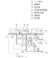
以下、従来の高周波信号受信装置について図面を用いて説明する。図6は、従来の高周波信号受信装置のブロック図である。図6において、アンテナ1は、約90MHzから770MHzまでのテレビ放送の放送信号(高周波信号の一例として用いた)が入力される。電子チューナ2は、入力端子2aから入力された放送信号を中間周波信号へと変換し、出力端子2bより出力するものである。
Hereinafter, a conventional high-frequency signal receiving device will be described with reference to the drawings. FIG. 6 is a block diagram of a conventional high-frequency signal receiving apparatus. In FIG. 6, the
電子チューナ2は、入力端子へ入力された放送信号が供給される増幅器3と、この増幅器3の出力と、局部発振器4からの信号とを混合する混合器5と、この混合器の出力が接続されたフィルタ6とを有していた。 The electronic tuner 2 is connected to an amplifier 3 to which a broadcast signal input to an input terminal is supplied, a mixer 5 that mixes an output of the amplifier 3 and a signal from the local oscillator 4, and an output of the mixer. Filter 6.
なお、局部発振器4には、PLL回路7がループ接続されている。さらに、局部発振器4と混合器5との間には、増幅器8が挿入されているものである。 Note that a PLL circuit 7 is loop-connected to the local oscillator 4. Further, an amplifier 8 is inserted between the local oscillator 4 and the mixer 5.
なお、この出願の発明に関連する先行技術文献情報としては、例えば、特許文献1、特許文献2が知られている。
しかしながらこのような従来の高周波信号受信装置を、温度変化幅の大きな自動車へ搭載される機器などへ用いた場合、局部発振器4の出力信号のレベルや増幅器3や増幅器8の利得が、温度変化により変動する。 However, when such a conventional high-frequency signal receiving apparatus is used in a device mounted on an automobile having a large temperature change range, the level of the output signal of the local oscillator 4 and the gains of the amplifier 3 and the amplifier 8 depend on the temperature change. fluctuate.
特に高温環境下においては、局部発振器4の出力レベルや増幅器3や増幅器8の利得が小さくなるので、混合器5へ入力される信号レベルが小さくなり、混合器5から出力される中間周波信号のNFが悪くなるという問題を有している。一方低温ではその逆に混合器5へ入力される信号のレベルが大きくなるので、混合器5が歪むこともある。 Particularly in a high temperature environment, the output level of the local oscillator 4 and the gains of the amplifier 3 and the amplifier 8 are reduced, so that the signal level input to the mixer 5 is reduced and the intermediate frequency signal output from the mixer 5 is reduced. There is a problem that NF deteriorates. On the other hand, at a low temperature, the level of the signal input to the mixer 5 increases, and the mixer 5 may be distorted.
そこで本発明は、この問題を解決したもので、温度変化に対しても安定して受信できる高周波信号受信装置を提供することを目的としたものである。 SUMMARY OF THE INVENTION The present invention solves this problem, and an object of the present invention is to provide a high-frequency signal receiving apparatus that can stably receive a temperature change.
この目的を達成するために本発明の高周波信号受信装置は、第2の増幅部の出力を供給する利得検出部と、この利得検出部の出力と前記第2の増幅部との間に利得制御部を設ける。そして、利得制御部は、利得検出部が検出した第2の増幅部の出力に応じて、第1の増幅部の利得を制御するものである。これにより、利得制御部は、利得検出部で検出された信号レベルが予め定められたレベルより小さい場合に、前記第1の増幅部の利得を大きくする方向へ制御するものである。 In order to achieve this object, a high frequency signal receiving apparatus according to the present invention includes a gain detection unit that supplies an output of a second amplification unit, and gain control between the output of the gain detection unit and the second amplification unit. Provide a part. The gain control unit controls the gain of the first amplifying unit according to the output of the second amplifying unit detected by the gain detecting unit. Thus, the gain control unit controls the gain of the first amplification unit to be increased when the signal level detected by the gain detection unit is smaller than a predetermined level.
以上のように本発明によれば、第2の増幅部の出力を供給する利得検出部と、この利得検出部の出力と前記第2の増幅部との間に挿入された利得制御部とを設け、前記利得検出部で検出された信号レベルが予め定められたレベルより小さい場合に、利得制御部が前記第1の増幅部の利得を大きくする方向へ制御するものである。 As described above, according to the present invention, the gain detection unit that supplies the output of the second amplification unit, and the gain control unit that is inserted between the output of the gain detection unit and the second amplification unit are provided. And when the signal level detected by the gain detector is smaller than a predetermined level, the gain controller controls the gain of the first amplifying unit to increase.
これにより、利得検出部が第2の増幅部から出力される信号の実際の出力レベルを検出し、この出力レベルが小さければ第1の増幅部の利得を制御するので、混合器へ入力されるレベルが安定する。 As a result, the gain detection unit detects the actual output level of the signal output from the second amplification unit, and if the output level is small, the gain of the first amplification unit is controlled, so that it is input to the mixer. Level stabilizes.
なお、利得制御部は、利得検出部で検出した出力信号のレベルが小さい場合、第1の増幅部の利得を大きくするので、特に高温時に出力レベルが小さくなることを防ぐことができる。従って、高温下においても安定して高周波信号を受信できる高周波信号受信装置を実現できる。特に高温環境下において、弱電界の放送を受信する場合の受信感度を良くできる。 Since the gain control unit increases the gain of the first amplification unit when the level of the output signal detected by the gain detection unit is small, the output level can be prevented from decreasing particularly at high temperatures. Therefore, it is possible to realize a high-frequency signal receiving apparatus that can stably receive a high-frequency signal even at high temperatures. In particular, in a high temperature environment, it is possible to improve the reception sensitivity when receiving a broadcast of a weak electric field.
このような高周波信号受信装置を、温度環境の厳しい自動車などに搭載すれば、たとえ機器が高温になっても、混合器の入力信号が小さくならないので、安定して受信できる自動車用受信機を実現できる。 If such a high-frequency signal receiver is installed in a car with a severe temperature environment, the input signal of the mixer does not become small even if the equipment gets hot, thus realizing a car receiver that can receive signals stably. it can.
近年、自動車の移動中における退屈凌ぎなどのために、後部座席にも液晶表示器などを設置し、それらの表示装置でテレビ放送などを視聴できるカーナビゲーション機器(以降カーナビという)などが登場してきている。そしてそのために、カーナビには、テレビ放送を受信するための高周波信号受信装置が内蔵されている。また、カーナビでは画面を見易くするためや、地図以外にも多くの情報を一度に表示するために、表示装置は大型化してきており、受信画像品質の良し悪しが、鮮明に判るようになってきている。従って、受信したテレビ放送に対し高画質化が求められることとなり、このような高周波信号受信装置に搭載される電子チューナに対しても、高い受信感度が求められるようになってきている。 In recent years, car navigation devices (hereinafter referred to as car navigation systems) that have installed liquid crystal displays in the rear seats and can be used to watch TV broadcasts, etc., have emerged in order to overcome boredom while moving cars. Yes. For this purpose, the car navigation system has a built-in high-frequency signal receiver for receiving television broadcasts. In addition, in order to make the screen easier to see in car navigation systems and to display a lot of information other than maps at once, display devices have become larger and the quality of received images has become clear. ing. Therefore, high image quality is required for the received television broadcast, and high reception sensitivity is also required for an electronic tuner mounted on such a high-frequency signal receiving apparatus.
さらに、カーナビなどのように自動車へ搭載される機器は、特に温度環境が厳しい。一般的にカーナビなどは、フロントガラスなどからの直射日光に直下に曝される場所に設置されるので、温度環境は非常に厳しい。そのためにこのような機器へ搭載される電子チューナには、広い温度範囲に対しても安定して受信できることが求められる。しかしこれまでの電子チューナは、屋内で使用されるテレビに用いられるものであったので、自動車のような広い温度範囲において安定した受信ができるものではなかった。そこで、本発明は、これらの要求を実現できる高周波信号受信装置を提供するためのものである。 Furthermore, devices mounted on automobiles such as car navigation systems have particularly severe temperature environments. In general, a car navigation system or the like is installed in a place exposed to direct sunlight from a windshield or the like, so the temperature environment is very severe. Therefore, an electronic tuner mounted on such a device is required to be able to receive stably over a wide temperature range. However, conventional electronic tuners have been used for televisions used indoors, and thus cannot be stably received over a wide temperature range like automobiles. Accordingly, the present invention is to provide a high-frequency signal receiving apparatus that can realize these requirements.
(実施の形態1)
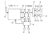
以下、実施の形態1におけるTV放送受信機(電子機器の一例として用いたものであり、上述したカーナビなども含むものである)について図面を用いて説明する。図2は、本実施の形態におけるTV放送受信機のブロック図である。図2において従来の構成と同じものは同じ番号を用いて、その説明は簡略化している。
(Embodiment 1)
Hereinafter, a TV broadcast receiver according to Embodiment 1 (used as an example of an electronic device and including the above-described car navigation system) will be described with reference to the drawings. FIG. 2 is a block diagram of the TV broadcast receiver in the present embodiment. In FIG. 2, the same components as those in the conventional configuration are denoted by the same reference numerals, and the description thereof is simplified.
アンテナ1は、90MHzから770MHzの周波数のテレビ放送波(高周波信号の一例として用いた)を受信する。アンテナ1で受信したテレビ放送波は、電子チューナ11(高周波信号受信装置の一例として用いた)の入力端子11aへ入力される。この電子チューナ11は、入力されたテレビ放送波の中から希望する周波数のチャンネルのみを選局し、500kHzの中間周波信号へ変換して出力端子11bから復調部12へ出力する。この復調部12は、電子チューナ11から出力された中間周波信号を復調する復調器12aと、この復調器12aの出力が接続され、復調された信号の誤り訂正を行う誤り訂正器12bとを有している。復調部12の出力は、復号部15へ接続され、復号部15によって音声データと映像データが再生される。なお、復調部12には、復調器12aの出力が供給された検波器13と、誤り訂正器12bの出力が接続され、誤り訂正器12bから出力される誤り率の値を判定する判定器14とを含んでいる。そして検波器13の出力は、電子チューナ11のAGC端子11cへ出力される。
The
復号部15で再生された映像データは、映像データ出力端子15aを介して表示部16へ供給される。ここで表示部16には、映像を表示させる液晶表示器16bと、この液晶表示器16bに接続された液晶駆動回路16aとを含み、液晶駆動回路16aでは復号部15から入力された映像データを蓄積し、1フレーム分の映像データが蓄積されると液晶表示器16bへ出力する。
The video data reproduced by the
一方、復号部15で再生された音声データは、音声データ出力端子15bから音声出力部17へ出力される。ここで音声出力部17は、スピーカ駆動回路17aと、このスピーカ駆動回路17aの出力が接続されたスピーカ17bとを含み、スピーカ駆動回路17aでは入力された音声データを音声信号へ変換し、スピーカ17bへ出力する。
On the other hand, the audio data reproduced by the
さらに、本実施の形態では、検波器13の出力と判定器14の出力とが接続されたマイクロコンピュータ18(以降マイコンと言う)を設け、このマイコン18から出力される制御信号は、電子チューナ11のデータ端子11dへと供給されている。なおマイコン18には、各種データを格納したメモリ19や、TV放送受信機への指令を入力する入力器20(入力キーやタッチパネルなど)などが接続されている。
Further, in the present embodiment, a microcomputer 18 (hereinafter referred to as a microcomputer) to which the output of the detector 13 and the output of the determiner 14 are connected is provided, and a control signal output from the
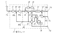
次に、本実施の形態における電子チューナ11の構成について、図面を用いて詳細に説明する。図1は、本実施の形態における電子チューナのブロック図である。図1において、フィルタ21には、入力端子11aに供給されたテレビ放送波が供給される。このフィルタ21は、テレビ放送波以外の不要な信号が、電子チューナ11へ供給されることを防ぐために設けられている。例えば、携帯電話などで利用されている800MHz帯の周波数信号を減衰するノッチフィルタなど、数種類のフィルタを含んでいる。
Next, the configuration of the electronic tuner 11 in the present embodiment will be described in detail with reference to the drawings. FIG. 1 is a block diagram of an electronic tuner according to the present embodiment. In FIG. 1, a television broadcast wave supplied to the
なお、このフィルタ21では、電子チューナ11の妨害となる不要な信号を充分に減衰させる。本実施の形態では、例えば携帯電話に利用される800MHz帯域の周波数信号を約60dB減衰させている。このようにすれば、後述する増幅部22と混合器23との間などへ別途フィルタなどを設けなくても良く、増幅部22と混合器23などを1つの集積回路24へ集積化することも可能となり、電子チューナ11の小型化を図ることができる。
The
増幅部22は、フィルタ21の出力が、集積回路24の端子24aを介して入力され、この入力されたテレビ放送波を増幅する。なお、増幅部22には、入力信号を約20dB増幅する低雑音増幅器を用いている。
The
増幅部22の出力は、利得制御増幅器25へ接続され、この利得制御増幅器25は、利得制御端子25aへ入力される制御信号により利得が変化するものである。なお、本実施の形態における利得制御増幅器25は、最大で約50dB変化するようにしている。
The output of the amplifying
利得制御増幅器25の出力は増幅部26へ接続されている。増幅部26は約10dBの増幅度を有し、増幅部22と同じ構成を有したものを用いている。混合器23の一方の入力には、増幅部26の出力が接続される。一方混合器23の他方の入力には、局部発振器27で発振した信号が、増幅部28を介して接続されている。なお、局部発振器27では約940MHzから1540MHzまでの信号を発振する。混合器23では、増幅部28で増幅された局部発振器27の発振信号と、増幅部26で増幅されたTV放送波とを混合し、500kHzの中間周波信号へと変換している。なお、本実施の形態における増幅部28には、入力された発振信号を約5dB増幅する低雑音増幅器を用いている。
The output of the
検波器29は、混合器23の出力が接続され、混合器23から出力された信号の総和の信号レベルに応じた直流電圧を出力する。AGC制御器30は、検波器29から出力された電圧が、予め定められたしきい値電圧より大きい場合に、その電圧差に応じた制御電圧を利得制御端子25aへ出力する。これによりいわゆるRFAGC回路が構成される。そしてこのRFAGC回路は、TV放送波のレベルが−50dBm以上である場合に動作する。ただし、TV放送波のレベルがそれ以下である場合は、利得制御増幅器25の利得は最大の利得で増幅するように制御されている。
The
なお、本実施の形態では、混合器23から出力された信号を検波したが、これは混合器23へ入力前のTV放送波の信号レベルを検波しても良い。この場合、混合器23へ注入されるTV放送信号のレベルを検出するので、混合器23が大きなレベルの妨害信号により歪まないように制御することが可能となる。
In this embodiment, the signal output from the
また、検波器29と混合器23との間に中間周波信号以外の周波数の信号を除去するフィルタ(後述する中間周波フィルタ31を用いても良い)を挿入しても良い。この場合、検波器29は希望チャンネル信号のレベルを検出できるので、希望チャンネルのTV放送波のレベルを精度良く制御できる。あるいは、これらを組み合わせて用いても良い。つまり、混合器23入力前のTV放送波のレベルと、希望チャンネル信号のレベルの双方を検波し、それらの信号のレベルに応じた各々の電圧をAGC制御器30へ入力する。この場合、妨害信号の有無などに応じ、さらに精度良い制御が可能となり、妨害などに対しても良好な受信感度を有した電子チューナ11が実現できる。
Further, a filter for removing a signal having a frequency other than the intermediate frequency signal (an
中間周波フィルタ31は、混合器23の出力が接続されている。この中間周波フィルタ31は、混合器23の出力から500kHzの周波数の中間周波信号のみを取り出すものである。
The output of the
なお、本実施の形態において、中間周波フィルタ31は集積回路の外に設けたが、これは集積回路に集積化しても良い。これによりさらなる小型化が可能となる。また、本実施の形態においては、BPFを用いたがLPFを用いても良い。これによりTV放送波のロスを少なくできる。
In the present embodiment, the
また、本実施の形態におけるIF周波数は、500kHzとしているが、携帯部分受信(1セグメント)の場合、約216kHzから約600kHzの範囲で中間周波数を選択すれば良い。これは、1segの周波数帯域が432kHzであるので、その周波数帯域半分の216kHz以上であることが必要となる。一方、上限の周波数は、復調LSIの対応周波数で決まるが周波数が高いと復調器に含まれたA/D変換回路などの消費電力が大きくなる。従って、本実施の形態におけるIF周波数は、500kHzとしている。これにより、消費電力を小さくできるので、携帯機器において機器の使用可能時間を長くできる。 Further, the IF frequency in the present embodiment is set to 500 kHz, but in the case of portable partial reception (one segment), an intermediate frequency may be selected in the range of about 216 kHz to about 600 kHz. Since the frequency band of 1 seg is 432 kHz, it is necessary that the frequency band is 216 kHz or more, which is half that frequency band. On the other hand, the upper limit frequency is determined by the corresponding frequency of the demodulation LSI, but if the frequency is high, power consumption of an A / D conversion circuit included in the demodulator increases. Therefore, the IF frequency in the present embodiment is set to 500 kHz. Thereby, since power consumption can be made small, the usable time of an apparatus can be lengthened in a portable apparatus.
さらに、本実施の形態では、携帯部分受信(1セグメント)時の中間周波数を適用しているが、携帯部分受信(3セグメント)および固定受信(13セグメント)にも適用可能であり、それぞれの周波数帯域幅は1296kHz、5.57MHzと携帯部分受信(1セグメント)と比較し周波数帯域幅が広くなるため、本実施の形態よりも中間周波数は高い構成となる。利得制御増幅器32は、中間周波フィルタの出力が接続され、利得制御端子32aへ供給される制御電圧に応じて利得が変化する。なお、本実施の形態における利得制御増幅器32は、最大で約20dB変化するようにしている。そして、この利得制御増幅器32の出力は、集積回路24の出力端子24bと、電子チューナ11の出力端子11bとを介して復調部12(図2に示す)へ出力される。
Furthermore, in this embodiment, the intermediate frequency at the time of mobile partial reception (1 segment) is applied, but it can also be applied to mobile partial reception (3 segments) and fixed reception (13 segments), and each frequency Since the bandwidth is 1296 kHz, 5.57 MHz, and the frequency bandwidth is wider than that of portable part reception (one segment), the intermediate frequency is higher than that of the present embodiment. The output of the intermediate frequency filter is connected to the
AGC制御器33は、復調部12内に集積化された検波器13の出力が、電子チューナ11のAGC端子11cと集積回路24の端子24cを介して供給される。ここで、検波器13は、復調器12aで復調された信号のレベルを検波し、その信号のレベルに応じた直流電圧を出力する。従って、AGC制御器33は、検波器13から出力された電圧が、予め定められたしきい値電圧より大きい場合に、その電圧差に応じた制御電圧を利得制御端子32aへ出力する。これによりいわゆるIFAGC回路が構成される。
The output of the detector 13 integrated in the demodulator 12 is supplied to the
そしてこのIFAGC回路は、TV放送波のレベルが−110dBmから−50dBmの間である場合に動作する。そして、TV放送波の−110dBm以下である場合に、利得制御増幅器25の利得は最大の利得で増幅し、−50dBm以上である場合に、利得制御増幅器25の利得は最小の利得で増幅するように制御されている。
The IFAGC circuit operates when the level of the TV broadcast wave is between −110 dBm and −50 dBm. When the TV broadcast wave is −110 dBm or less, the gain of the
次に、検波器34(利得検出部の一例として用いた)は、増幅部28の出力が接続され、増幅部28で増幅された発振信号のレベルに応じた電圧を出力する。利得制御部35には、この検波器34の出力が接続され、この検波器34から出力された電圧と予め定められた基準電圧との差に応じた制御信号を出力する。そして、この利得制御部35から出力された制御信号は、増幅部22と、増幅部26及び増幅部28とへ供給され、それらの利得を変化させている。
Next, the detector 34 (used as an example of the gain detection unit) is connected to the output of the
なお、マイコン18(図2に示す)の出力は、電子チューナ11のデータ端子11dを介して集積回路24のデータ端子24dと端子24eとへ接続されている。そして、データ端子24dは、局部発振器27にループ接続されたPLL回路36へ接続される。一方、端子24eは利得制御部35へ接続されている。
The output of the microcomputer 18 (shown in FIG. 2) is connected to the
なお、本実施の形態では、以上に説明した電子チューナ11中のフィルタ21と中間周波フィルタ31以外は集積回路24内に集積化されている。これにより小型な電子チューナを実現できる。
In the present embodiment, the components other than the
以上のように構成されたTV放送受信機において、まずは、常温の温度環境下(例えば25℃)で、かつ通常に受信が可能な電界強度(いわゆる中電界といい、例えば放送波のレベルとして−60dBm)のTV放送を受信する場合における電子チューナ11の動作を説明する。 In the TV broadcast receiver configured as described above, first, an electric field intensity (so-called medium electric field) that can be normally received under a normal temperature environment (for example, 25 ° C.), for example, as a broadcast wave level − The operation of the electronic tuner 11 when receiving a 60 dBm TV broadcast will be described.
アンテナ1で受信された高周波信号からフィルタ21でTV放送波以外の不要な信号を除去する。そして増幅部22は、TV放送波を約20dB増幅する。利得制御増幅器25を含むRFAGC回路により規定のレベルへ調節された信号は、混合器23へ供給される。この混合器23では、TV放送波と局部発振器27の出力と混合するものである。なお、局部発振器27は、PLL回路がマイコン18からの選局データによって制御され、受信希望チャンネルの周波数が500kHzの中間周波信号となるような周波数を発振する。
An unnecessary signal other than the TV broadcast wave is removed from the high-frequency signal received by the
そしてさらに、利得制御増幅器32を含むIFAGC回路によって、復調器12aでの復調信号のレベルが一定となるように制御される。このようにして一定の信号レベルとされ、復調器で正常に復調されたTV放送信号は、誤り訂正器12bで誤りが訂正され、復号部15でH.264など伸長されて、元の映像信号と音声信号とが正常に再生される。これにより液晶表示器16bとスピーカ17bとから正常な画像と音声が出力される訳である。
Further, the IFAGC circuit including the
一方、放送局からの距離が遠い場所でTV放送を受信するような場合、TV放送波の電界強度は弱い(いわゆる弱電界であり、例えば、−100dBm)。例えば、本実施の形態においてIFAGCが動作を開始するレベル(−110dBmであり、以下このレベルをIFAGC動作点という)のTV放送波を受信する場合、利得制御増幅器25、利得制御増幅器32の利得は、共に最大となる。これにより弱電界のTV放送波を受信した場合の中間周波信号のレベルも、中電界である場合と同じレベルとなり、正常に受信が可能となる。
On the other hand, when a TV broadcast is received at a location far from the broadcast station, the electric field intensity of the TV broadcast wave is weak (so-called weak electric field, for example, −100 dBm). For example, in the present embodiment, when receiving a TV broadcast wave at a level at which IFAGC starts operating (−110 dBm, this level is hereinafter referred to as an IFAGC operating point), the gains of the
次に、高温環境下(例えば85℃)において、IFAGC動作点のTV放送波を受信する場合について説明する。一般的に増幅器は、温度に応じて利得が変動する。具体的には、高い温度において、利得が小さくなり、低い温度において、利得が大きくなる。 Next, a case where a TV broadcast wave at the IFAGC operating point is received in a high temperature environment (for example, 85 ° C.) will be described. In general, the gain of an amplifier varies with temperature. Specifically, the gain decreases at a high temperature and increases at a low temperature.
従って、高温下において増幅部22、26に用いる増幅器の利得は、減少する。また、局部発振器27には差動増幅器などを有しているので、局部発振器27の出力信号自体のレベルも小さくなる。この状況下で、例えばIFAGC動作点のTV放送波を受信する場合、利得制御増幅器25、32は、既に最大利得となっているので、増幅部22、26の利得減少分や、局部発振器27の信号レベル低下分を補うことはできない。
Therefore, the gain of the amplifier used for the
一方、低温環境下においては、逆に大きなレベルの信号が入力された場合に問題が発生する。つまり、RFAGCやIFAGCが共に最小利得で制御されている状態において、温度が低い(例えば−40℃)場合、増幅部28の利得や、局部発振器27の信号レベルが大きくなり、混合器23などへ入力される信号のレベルは大きくなる。これにより増幅部22、26や混合器23が飽和し、TV放送信号に歪みが発生し易くなる。
On the other hand, in a low temperature environment, a problem occurs when a large level signal is input. That is, in the state where both RFAGC and IFAGC are controlled with the minimum gain, when the temperature is low (for example, −40 ° C.), the gain of the
そこで本発明における利得制御部35は、検波された増幅部28の出力信号のレベルに応じ、増幅部28の利得をフィードバック制御するものである。これにより、増幅部28から出力された信号レベルが小さければ、増幅部22、26、28の利得を大きくし、逆にその信号レベルが大きければ、増幅部22、26、28の利得を小さくするものである。
Therefore, the
具体的には、増幅部28の出力を検波器34へ供給する。検波器34では、増幅部28から出力される実際の信号の信号レベルを検出する。そして、この検波器34の出力を利得制御部35へ供給する。検波器34は、入力された信号のレベルに応じた電圧の信号を出力するので、利得制御部35は、検波器34の出力電圧と予め定められた基準電圧とを差動増幅器などにより比較することで、常温との温度差に対応する電圧差を得ることができる。そしてこの電圧差に対応した制御信号を増幅部22、26、28へ供給することにより、これらの増幅部22、26、28の利得を変化させるわけである。これにより、温度が低くなった場合においても、増幅部28からの出力が小さくなることを防ぐことができる。従って、低温環境下においても弱電界のTV放送波を感度良く受信することができる。
Specifically, the output of the amplifying
なお、本実施の形態では、常温状態において検波器34が出力すべき電圧値を基準電圧として設定している。これにより、温度変動がある場合においても、常に常温と同じ状態の信号レベルを維持できる。
In the present embodiment, the voltage value to be output by the
以上の構成により、混合器23へ入力される発振信号のレベルは、温度の変化に対して変動し難くなる。従って、中間周波信号や復調信号のレベルは、温度環境による影響が小さくなるので、温度変化に対しNFや受信感度が良好であり、かつ歪みなどが発生し難い電子チューナを実現できる。
With the above configuration, the level of the oscillation signal input to the
つまりこれにより、特に温度環境の厳しい自動車などに搭載される高周波信号受信装置などにおいて、温度環境が変化しても安定した受信品質でTV放送の受信ができるTV放送受信機を提供できることとなる。従って特に、本発明の電子チューナ11は、特にカーナビへ内蔵されるテレビ放送受信用チューナなどへ用いると良い。 In other words, this makes it possible to provide a TV broadcast receiver that can receive TV broadcasts with stable reception quality even when the temperature environment changes, such as in a high-frequency signal receiver mounted in a car or the like having a particularly severe temperature environment. Therefore, in particular, the electronic tuner 11 of the present invention is preferably used for a TV broadcast receiving tuner built in a car navigation system.
本実施の形態では、局部発振器27に接続された増幅部28の利得を安定化させているが、これは、上述したように局部発振器27と増幅部28が共に温度変動による影響を受けやすいので、温度に対する信号レベルの変化量も大きいためである。これにより温度変動に対する検波器34の感度が良くなる。従って、温度変動に対して精度の良い制御が可能となる。
In the present embodiment, the gain of the amplifying
なお、本実施の形態では、利得制御部35は、増幅部22や増幅部26も同様に制御している。これは、温度が高いと利得が小さくなり、温度が低いと利得が大きくなるからである。つまり、温度に対し増幅部22、26は、増幅部28と同じ傾向で利得変化するためであるので、利得制御部35は、検波器34からの出力が基準値より大きい場合には、増幅部22、26および増幅部28の利得が小さくなる方向へ制御する。逆に、利得制御部35は、検波器34からの出力が基準値より小さい場合には、増幅部22、26および増幅部28の利得が大きくなる方向へ制御する。
In the present embodiment, the
これにより、増幅部22、26も温度変動による利得変動を小さくできるので、電子チューナ11は、さらに温度変化に対して中間周波信号や復調信号のレベルが安定する。従って温度変化による受信品質への影響を受け難いTV放送受信機を実現できる。なお、本実施の形態ではTV放送受信機を例に説明したが、局部発振回路が内蔵されているGPS、携帯電話用無線装置、Bluetooth、W−LAN等の高周波信号受信装置においても適用可能である。
As a result, since the
また、本実施の形態においてマイコン18には、復調器12aの信号レベルを検波する検波器13と、誤り訂正器12bでのビット誤り率を判定する判定器14の出力が接続されている。マイコン18はこれらの情報から、受信品質が悪いと判定した場合に、利得制御部35を動作させる旨の信号を送出する。この信号は、利得制御部35の電源供給端子に設けられたスイッチ(図示せず)へ供給される。これにより、このスイッチをオンとすることで、利得制御部35が動作し、増幅部22、26、28を制御する。このように、受信品質が良い場合には、利得制御部35をオフとすることにより、消費電力を減らしている。これは、特にバッテリや電池駆動するような携帯型のTV放送受信機において有用となる。
In the present embodiment, the
さらに、増幅部22、26、28には、例えば低雑音増幅器と利得制御増幅器との直列接続体を用いることや、低雑音増幅器と定電流源回路による構成などを用いれば良い。例えば、利得制御増幅器を用いた場合には、増幅部の利得可変範囲が大きく、かつ精度良く制御可能であるので、温度変動が広くても安定した受信が可能となる。
Further, for the amplifying
さらにまた、利得制御部35の基準電圧は、マイコン18に接続されたメモリ19に記憶させている。これにより、各個体毎に、当該の個体に最適な基準電圧の設定が可能となるので、最適なレベルで制御が可能となる。
Furthermore, the reference voltage of the
さらに加えて、本実施の形態では、アンテナ1と電子チューナ11、復調部12は、全て1系統であり、増幅部28は、1つの混合器23へのみ信号を供給している。しかし、カーナビなどのような移動体機器へ搭載される高周波信号受信装置においては、アンテナ1、電子チューナ11や復調部12を2系統以上用いるダイバーシティ方式が用いられるが、本発明は、このようなダイバーシティ方式に用いても良い。つまり、もうひとつの電子チューナ(図示せず)に対して局部発振器27、増幅部28を共用し、利得制御部35はこの増幅部28を制御するものである。これにより、局部発振器が1つでよいので低価格な高周波受信装置を実現することができる。そして、双方の電子チューナは、温度変化に対して混合器への入力信号レベルの変化は小さくなる。
In addition, in this embodiment, the
また、本実施の形態において利得制御部35は、増幅部28、22、26の利得を制御したが、これ以外に有した増幅部に対して制御する構成としても良い。そのようにすれば、さらに温度変化に対する信号レベル変化が小さくなるので、良好なNFを実現できる。
In this embodiment, the
(実施の形態2)
以下、実施の形態2について図面を用いて説明する。図3は、本実施の形態における利得制御部と増幅部のブロック図であり、図1や図2と同じものは同じ番号を用い、その説明は簡略化している。なお、本実施の形態における利得制御部41と増幅部42とは、実施の形態1における利得制御部35と増幅部28との他の実施の形態を示すものであるので、その部分に関して詳細に説明する。
(Embodiment 2)
The second embodiment will be described below with reference to the drawings. FIG. 3 is a block diagram of the gain control unit and the amplification unit in the present embodiment. The same components as those in FIGS. 1 and 2 are denoted by the same reference numerals, and the description thereof is simplified. The
まず、本実施の形態における利得制御部41について説明する。端子43には、検波器34の出力が接続される。一方端子44には、基準電圧が供給されている。なお、基準電圧は、常温時における検波器34の出力電圧と同じ電圧としている。差動増幅器45は、端子43と端子44から入力された電圧を比較し、その差に応じた差電圧を出力する。加算器46は、電源に接続された端子47から供給される電源電圧と差電圧とを加算し、端子48から出力する。
First, the
そして、利得制御部41は、端子43から入力された検波器34の出力電圧が、予め定めた基準電圧よりも小さい場合には、その差電圧分だけ端子48から出力する電圧を大きくし、逆に、利得制御部41は、端子43から入力された検波器34の出力電圧が、予め定めた基準電圧よりも大きい場合には、その差電圧分だけ端子48から出力する電圧を小さくする。
When the output voltage of the
次に、増幅部42について説明する。増幅部42には、局部発振器27と混合器23との間に挿入された増幅器51と、定電流源回路52とを含んでいる。この定電流源回路52は、電源供給端子53へ電圧を供給すると、一定の電流が定電流出力端子54から出力されるものである。そして、定電流出力端子54を増幅器51の電源端子51aへ接続している。
Next, the
では、定電流源回路52(電源電圧依存型の定電流源回路の一例として用いた)について説明する。電源供給端子53へ供給された電源電圧は、抵抗55を介してトランジスタ56のベースとトランジスタ57のコレクタに供給される。一方定電流出力端子54は、トランジスタ56、58のコレクタに接続される。トランジスタ56のエミッタ出力は、トランジスタ57、58のベースへ接続されている。なお、これらトランジスタ56、57、58のエミッタとグランドとの間には、夫々抵抗59、60、61が挿入されている。
Now, the constant current source circuit 52 (used as an example of a power source voltage dependent constant current source circuit) will be described. The power supply voltage supplied to the
次に、この増幅部42の動作について説明する。この定電流源回路52は、電源供給端子53に供給される電圧に応じ、定電流出力端子54から出力される電流が変化する(本発明では、このような定電流源回路を電源電圧依存型の定電流源回路と呼ぶ。)。ただしこの場合、抵抗55、抵抗59、60、61との関係は(数1)の関係とする。
Next, the operation of the amplifying

このようにすれば、トランジスタ57とトランジスタ58とのコレクタ電流は、等しくなり、定電流出力端子54へ流れる電流は、(数2)の関係で示される。
By doing so, the collector currents of the
以上のように、定電流源回路52は、電源供給端子53に供給される電圧に応じ、定電流出力端子54から出力される電流が変化することとなる。そこで、利得制御部41の端子48を電源供給端子53へ接続する。これにより、利得制御部41が、電源供給端子53へ供給する電圧を変化させることによって、増幅器51へ供給する電流を変化させることができる訳である。
As described above, the constant
このような構成とすることで、例えば温度が常温から高くなった場合、局部発振器27の信号レベルや、増幅器51の利得が小さくなるので、増幅器51から出力される信号のレベルも小さくなる。そこで、利得制御部41は、検波器34から入力された電圧により増幅器51から出力された信号レベルが小さくなったことを検出する。そして利得制御部41では、差動増幅器45が、常温時の検波器の出力レベルを基準電圧として、この基準電圧と検波器34の出力電圧との差電圧を加算器46へ出力し、この加算器46で差電圧と電源電圧とを合成する。これにより、定電流源回路52の電源供給端子53へ供給する電圧を大きくする。
With such a configuration, for example, when the temperature is increased from room temperature, the signal level of the
定電流源回路52は、電源電圧依存型の定電流源回路を用いているので、電源供給端子53へ供給する電圧を大きくすると、定電流出力端子54から出力する電流が大きくなる。従って、増幅器51の電源端子51aへ供給する電流が大きくなり、増幅器51の利得が大きくなるわけである。
Since the constant
逆に温度が常温よりも低温である場合には、増幅器51から出力される信号レベルが大きくなり、電源供給端子53へ供給する電圧を小さくするので、定電流出力端子54から出力される電流は小さくなる。従って、利得制御部41は、増幅器51の電源端子51aへ供給する電流を小さくするので、増幅器51の利得が小さくなる方向へ制御されるわけである。
Conversely, when the temperature is lower than room temperature, the signal level output from the
なお、定電流源回路52には、電源電圧依存型の定電流源回路を用いているので、電源電圧による電流の変動はあるが、温度による定電流出力端子に流れる電流の変化は小さい。従って、温度変化に対して定電流源回路52の変動を小さくできる。さらに、利得制御部41は、増幅器51の利得をフィードバック制御しているので、電源電圧変動などに対して、増幅器51の出力レベルを安定させることができる。
Since the constant
また、この増幅部42は、実施の形態1における増幅部22や、増幅部26に用いても良い。この場合、利得制御部41の端子を増幅部22や増幅部26の電源端子へ接続する。ただし、増幅部42とは必要とされる利得などが異なるので、その場合には、端子48と夫々の増幅部22、26との間に、それぞれの増幅部22、26に適した抵抗値の抵抗を挿入する。
Further, the
(実施の形態3)
以下に実施の形態3について図面を用いて説明する。図4は、本実施の形態における増幅部と利得制御部とのブロック図である。図4において、図1から図3と同じものは同じ番号を用いて、その説明は簡略化している。なお、本実施の形態における利得制御部71と増幅部72とは、実施の形態1における利得制御部35と増幅部28との他の実施の形態を示すものであるので、その部分に関して詳細に説明する。
(Embodiment 3)
Embodiment 3 will be described below with reference to the drawings. FIG. 4 is a block diagram of the amplification unit and gain control unit in the present embodiment. 4, the same components as those in FIGS. 1 to 3 are denoted by the same reference numerals, and the description thereof is simplified. The
まず、本実施の形態における利得制御部71について説明する。端子73には、検波器34の出力が接続される。一方端子74には、基準電圧が供給されている。なお、この基準電圧は、常温時における検波器34の出力電圧と同じ電圧であり、この基準値が、メモリ75に格納されている。差動増幅器76は、端子73と端子74から入力された電圧を比較し、その差に応じた差電圧を出力する。判定器77は、差動増幅器76の出力が接続され、差電圧に応じた制御信号を発生させ、この制御信号を端子78から出力する。
First, the
次に、増幅部72について説明する。増幅部72には、局部発振器27と混合器23との間に挿入された増幅器81と、定電流源回路82とを含んでいる。この定電流源回路82は、電源供給端子83へ電圧を供給すると、一定の電流が定電流出力端子84から出力されるものである。そして、定電流出力端子84を増幅器81の電源端子81aへ接続している。
Next, the
では、定電流源回路82(ベース・エミッタ電圧依存型の定電流源回路の一例として用いた)について説明する。電源供給端子83へ供給された電源電圧は、抵抗85を介してトランジスタ86のベースと、トランジスタ87のコレクタとベースとへ供給される。トランジスタ87のエミッタが、トランジスタ88のコレクタとベースとへ接続され、このトランジスタ88は、エミッタ接地されている。
The constant current source circuit 82 (used as an example of a base / emitter voltage dependent constant current source circuit) will be described. The power supply voltage supplied to the
トランジスタ86のコレクタは、定電流出力端子84へ接続される。一方、トランジスタ86のエミッタには、切替えスイッチ89の共通端子89aが接続されている。そしてこの切替えスイッチの端子89b、89c、89dとグランドとの間の夫々には抵抗90、91、92が挿入されている。利得制御部71の端子78は、切替えスイッチ89の切替え制御端子89eへ接続されている。
The collector of the
次に、この増幅部72の動作について説明する。この定電流源回路82は、電源供給端子83に供給される電圧によらず、定電流出力端子84から出力される電流は一定となる。ただし、トランジスタ86、87、88のベース・エミッタ間の電圧に応じて、定電流出力端子84から出力される電流が変化する(本発明では、このような定電流源回路をベース・エミッタ電圧依存型の定電流源回路と呼ぶ。)。
Next, the operation of the amplifying
このようにすれば、トランジスタ86、87、88のベース・エミッタ間の電圧は、等しくなり、定電流出力端子84へ流れる電流は、(数3)の関係で示される。
In this way, the base-emitter voltages of the
従って、この定電流源回路82において、定電流出力端子84から出力される電流を変化させるためには、トランジスタ86のエミッタ抵抗の値を変化させれば良い訳である。そこで、エミッタ抵抗90、91、92を切替えるために、切替えスイッチ89の切替え制御端子89eと利得制御部71の端子78とを接続する。そして判定器77には、メモリ75を接続し、このメモリ75には、差動増幅器76からの差電圧の値と切替えスイッチとの関連が、テーブルとして格納されている。これにより、判定器77は、テーブルから差動増幅器76の差電圧に応じた制御信号を発生させ、切替えスイッチ89を切替えるものである。
Therefore, in the constant
これにより、利得制御部71から出力された制御信号によって、切替えスイッチ89が切替えられることとなり、増幅器81へ供給する電流を変化させることができる訳である。
As a result, the
このような構成とすることで、例えば温度が常温から高くなった場合、局部発振器27の信号レベルや、増幅器81の利得が小さくなるので、増幅器81から出力される信号のレベルも小さくなる。そこで、利得制御部71は、検波器34から入力された電圧により増幅器81から出力された信号レベルが小さくなったことを検出する。そして利得制御部71では、差動増幅器76が、常温時の検波器の出力レベルを基準電圧として、この基準電圧と検波器34の出力電圧との差電圧を判定器77へ出力し、この判定器77で差電圧に応じて、切替えスイッチ89を切替える為の制御信号を出力する。そして、抵抗90、91、92の中の適した抵抗値を有した抵抗を選択する。
With such a configuration, for example, when the temperature is increased from room temperature, the signal level of the
このように、定電流源回路82は、ベース・エミッタ電圧依存型の定電流源回路を用いているので、トランジスタ86のエミッタ抵抗を小さくすると、定電流出力端子84から出力する電流が大きくなる。従って、判定器77は、増幅器81から出力される信号のレベルが小さい場合には、常温時に選択していた抵抗よりも小さな抵抗値の抵抗を選択するように指示をする。これにより、定電流出力端子から出力される電流が大きくなるので、増幅器81の電源端子81aへ供給される電流が大きくなり、増幅器81の利得が大きくなるわけである。
Thus, the constant
逆に温度が常温よりも低温である場合、増幅器81から出力される信号のレベルが大きくなる。そしてこのような場合、判定器77は、常温時に選択していた抵抗よりも大きな抵抗値の抵抗を選択するように指示をする。これにより、定電流出力端子から出力される電流が小さくなるので、増幅器81の電源端子81aへ供給される電流を小さくし、増幅器81の利得は、小さくなる方向へ制御されるわけである。
On the contrary, when the temperature is lower than the normal temperature, the level of the signal output from the
なお、定電流源回路82には、ベース・エミッタ電圧依存型の定電流源回路を用いているので、温度による電流の変動はあるが、電源電圧による定電流出力端子に流れる電流の変化は小さい。従って、電源電圧の変動に対して定電流源の変動を小さくできる。さらに、利得制御部71は、増幅器81の利得をフィードバック制御しているので、温度変化に対しても、増幅器81の出力レベルを安定させることができる。
Since the constant
なお、基準値をメモリ75へ格納しているので、常温時の増幅器81の利得ばらつきや、常温時の局部発振器27の発振レベルばらつきなど、個体ばらつきに応じて基準値を設定できる。これにより、常温時の増幅器81の利得ばらつきや、常温時の局部発振器27の発振レベルばらつきなどがあっても、混合器23へ供給する信号のレベルを一定のレベルに保つことができる。従って、個体毎に、NFを最適にすることができる。
Since the reference value is stored in the
また、この増幅部72は、実施の形態1における増幅部22や、増幅部26に用いても良い。この場合、利得制御部71の端子を増幅部22や増幅部26の電源端子へ接続する。ただし、増幅部42とは必要とされる利得などが異なるので、その場合には、メモリ75に夫々の増幅部22、26から出力するためのテーブルを個別に持たせても良い。あるいは、トランジスタ86のエミッタ抵抗の値で調整しても良い。
Further, the
(実施の形態4)
以下の実施の形態4について図面を用いて説明する。図5は、本実施の形態における高周波信号受信装置のブロック図である。図5において図1や図2と同じものは同じ番号を用いて、その説明は簡略化している。
(Embodiment 4)
The following fourth embodiment will be described with reference to the drawings. FIG. 5 is a block diagram of the high frequency signal receiving apparatus according to the present embodiment. In FIG. 5, the same components as those in FIGS. 1 and 2 are denoted by the same reference numerals, and the description thereof is simplified.
本実施の形態における電子チューナ11では、フィルタ21の出力が接続された増幅部101は、集積回路102外に構成している。なお増幅部101の電源端子101aには、利得制御部35の出力が端子102dを介して接続されている。ここで、増幅部101は、集積回路102とは異なったプロセスで作成したものである。これにより、増幅部101には、特に高周波特性を重要視し、例えばガリウム・砒素などによる増幅器を使用できるので、NFなどの良好な高周波信号受信装置を実現できる。
In the electronic tuner 11 according to the present embodiment, the
一方、集積回路102には低価格なプロセスを用いることも可能となるので、低価格な電子チューナ11を実現できる。さらに集積化されているので、小型の電子チューナを実現できる。
On the other hand, since it is possible to use a low-cost process for the
なお、本実施の形態では、増幅部101が集積回路102外に出されている分、実施の形態1に比べてサイズが大きくなる。そこで、この面積増加を補う為に、中間周波フィルタ31を集積回路102内に集積化している。これにより電子チューナ11のサイズを大きくすることなく、小型の電子チューナを実現できる。
In the present embodiment, the size of the amplifying
さらに増幅部101と集積回路102の入力端子102aとの間にはフィルタ103を挿入している。これによりTV放送波のロスを小さくできるので、受信感度の良好な電子チューナ11を実現できる。
Further, a
本発明にかかる高周波信号受信装置は、温度が変化しても安定して受信できるという効果を有し、TV付きカーナビなどのように自動車へ搭載される機器等へ用いる高周波信号受信装置として有用である。 The high-frequency signal receiving apparatus according to the present invention has an effect of being able to receive stably even when the temperature changes, and is useful as a high-frequency signal receiving apparatus used for equipment mounted on an automobile such as a car navigation system with a TV. is there.
11a 入力端子
22 増幅部
23 混合器
25 利得制御増幅器
27 局部発振器
28 増幅部
34 検波器
Claims (2)
前記入力端子の出力側に接続されると共に、前記入力端子に入力された前記高周波信号が供給される第1の増幅部と、
局部発振器と、
前記局部発振器の出力側に接続されると共に、前記局部発振器の出力が供給される第2の増幅部と、
前記第1の増幅部の出力側に接続されかつ前記第2の増幅部の出力側に接続されて、前記第1の増幅部の出力が一方の入力に供給されるとともに、他方の入力には前記局部発振器の出力が前記第2の増幅部を介して供給される混合器と、
前記混合器の出力が供給される出力端子と、
前記第2の増幅部の出力側に接続されると共に、前記第2の増幅部の出力が供給される利得検出部と、
前記利得検出部の出力と前記第2の増幅部の他方の入力との間に挿入されて、前記利得検出部からの出力電圧と予め定められた基準電圧とを比較することで、温度変動に対応する電圧差を得て、前記電位差に対応した制御信号を前記第2の増幅部の他方の入力を介して前記第2の増幅部に入力することで、前記第2増幅部の利得を変化させる利得制御部とを有し、
前記第1の増幅部の他の入力は、前記利得制御部の他の出力に接続されると共に、
前記利得制御部は、前記電位差に対応した制御信号を前記利得制御部の他の出力から出力して前記第1の増幅部の他の入力に入力することで、前記利得検出部で検出された信号レベルが予め定められたレベルより小さい場合には、前記第1の増幅部の利得を大きくする方向へ制御する高周波信号受信装置。 An input terminal for receiving a high-frequency signal;
A first amplifier connected to the output side of the input terminal and supplied with the high-frequency signal input to the input terminal;
A local oscillator,
A second amplifier connected to the output of the local oscillator and supplied with the output of the local oscillator;
Connected to the output side of the first amplifying unit and connected to the output side of the second amplifying unit, the output of the first amplifying unit is supplied to one input, and the other input A mixer in which the output of the local oscillator is supplied via the second amplifier;
An output terminal to which the output of the mixer is supplied;
A gain detector connected to the output side of the second amplifying unit and supplied with the output of the second amplifying unit;
Inserted between the output of the gain detection unit and the other input of the second amplification unit, and by comparing the output voltage from the gain detection unit with a predetermined reference voltage, the temperature variation By obtaining a corresponding voltage difference and inputting a control signal corresponding to the potential difference to the second amplifying unit via the other input of the second amplifying unit, the gain of the second amplifying unit is changed. A gain control unit
The other input of the first amplification unit is connected to the other output of the gain control unit,
The gain control unit is detected by the gain detection unit by outputting a control signal corresponding to the potential difference from the other output of the gain control unit and inputting the control signal to the other input of the first amplification unit . A high-frequency signal receiving apparatus that controls to increase the gain of the first amplifying unit when the signal level is lower than a predetermined level.
前記アンテナの出力側に接続されると共に、前記アンテナに入力された前記高周波信号が供給される請求項1に記載の高周波信号受信装置と、
前記高周波信号受信装置の出力側に接続された復調器と、
前記復調器の出力側に接続された復号部と、
前記復号部の出力側に接続された表示部とを備えた電子機器。 An antenna to which a high-frequency signal is input;
The high-frequency signal receiving device according to claim 1, wherein the high-frequency signal is connected to an output side of the antenna and the high-frequency signal input to the antenna is supplied.
A demodulator connected to the output side of the high-frequency signal receiver;
A decoding unit connected to the output side of the demodulator;
An electronic apparatus comprising: a display unit connected to an output side of the decoding unit.
Priority Applications (1)
| Application Number | Priority Date | Filing Date | Title |
|---|---|---|---|
| JP2005012293A JP4470744B2 (en) | 2005-01-20 | 2005-01-20 | High frequency signal receiver and electronic device using the same |
Applications Claiming Priority (1)
| Application Number | Priority Date | Filing Date | Title |
|---|---|---|---|
| JP2005012293A JP4470744B2 (en) | 2005-01-20 | 2005-01-20 | High frequency signal receiver and electronic device using the same |
Publications (2)
| Publication Number | Publication Date |
|---|---|
| JP2006203487A JP2006203487A (en) | 2006-08-03 |
| JP4470744B2 true JP4470744B2 (en) | 2010-06-02 |
Family
ID=36961098
Family Applications (1)
| Application Number | Title | Priority Date | Filing Date |
|---|---|---|---|
| JP2005012293A Expired - Fee Related JP4470744B2 (en) | 2005-01-20 | 2005-01-20 | High frequency signal receiver and electronic device using the same |
Country Status (1)
| Country | Link |
|---|---|
| JP (1) | JP4470744B2 (en) |
Families Citing this family (2)
| Publication number | Priority date | Publication date | Assignee | Title |
|---|---|---|---|---|
| JP5077087B2 (en) * | 2008-06-16 | 2012-11-21 | カシオ計算機株式会社 | Radio receiver and radio clock |
| JP5320841B2 (en) * | 2008-06-17 | 2013-10-23 | 住友電気工業株式会社 | Amplifier and optical module |
-
2005
- 2005-01-20 JP JP2005012293A patent/JP4470744B2/en not_active Expired - Fee Related
Also Published As
| Publication number | Publication date |
|---|---|
| JP2006203487A (en) | 2006-08-03 |
Similar Documents
| Publication | Publication Date | Title |
|---|---|---|
| US7454180B2 (en) | Vehicle-mounted receiving apparatus for reducing distortion, improving reception sensitivity, and saving power | |
| JP2006050585A (en) | Digital broadcast receiver unit, and automatic gain control circuit | |
| JP4350689B2 (en) | Tuner circuit and digital broadcast receiver | |
| JP4529092B2 (en) | Tuner device | |
| JP4470744B2 (en) | High frequency signal receiver and electronic device using the same | |
| JP4238210B2 (en) | Diversity receiver | |
| US20070155351A1 (en) | Receiving apparatus | |
| JP4480555B2 (en) | Tuner circuit and digital broadcast receiver including the same | |
| JP2006203488A (en) | High frequency signal receiver, integrated circuit used for same and electronic equipment using receiver | |
| JP2006203489A (en) | High frequency signal receiver, integrated circuit for use therein, and electronic apparatus employing high frequency signal receiver | |
| US20070218944A1 (en) | System and method for receiving wireless signals | |
| US20050143030A1 (en) | Receiving apparatus | |
| KR100872550B1 (en) | Auto gain control circuit of tuner | |
| JP3891183B2 (en) | Portable high frequency receiver and integrated circuit used therefor | |
| JP4249007B2 (en) | Receiving device, tuner and tuner management device | |
| JP2007067471A (en) | Electronic tuner, high-frequency signal receiver using the same, and control method thereof | |
| EP1835735A1 (en) | System and method for receiving wireless signals | |
| JP2005123859A (en) | Digital broadcasting receiving device | |
| JP2008085873A (en) | Radio receiver | |
| JP3995607B2 (en) | Broadcast wave receiver | |
| JP2008141580A (en) | On-board diversity receiver and its receiving method | |
| KR100716139B1 (en) | Auto Gain Control Circuit for Digital Tuner | |
| JP2010109560A (en) | Receiver, semiconductor device, communication device and electronic device | |
| JPH0823482A (en) | Antenna controller | |
| JP2000232389A (en) | Tuner for digital signal reception |
Legal Events
| Date | Code | Title | Description |
|---|---|---|---|
| A621 | Written request for application examination |
Free format text: JAPANESE INTERMEDIATE CODE: A621 Effective date: 20080121 |
|
| RD01 | Notification of change of attorney |
Free format text: JAPANESE INTERMEDIATE CODE: A7421 Effective date: 20080213 |
|
| A977 | Report on retrieval |
Free format text: JAPANESE INTERMEDIATE CODE: A971007 Effective date: 20090717 |
|
| A131 | Notification of reasons for refusal |
Free format text: JAPANESE INTERMEDIATE CODE: A131 Effective date: 20090818 |
|
| A521 | Written amendment |
Free format text: JAPANESE INTERMEDIATE CODE: A523 Effective date: 20091016 |
|
| RD01 | Notification of change of attorney |
Free format text: JAPANESE INTERMEDIATE CODE: A7421 Effective date: 20091120 |
|
| A131 | Notification of reasons for refusal |
Free format text: JAPANESE INTERMEDIATE CODE: A131 Effective date: 20091124 |
|
| A521 | Written amendment |
Free format text: JAPANESE INTERMEDIATE CODE: A523 Effective date: 20100118 |
|
| TRDD | Decision of grant or rejection written | ||
| A01 | Written decision to grant a patent or to grant a registration (utility model) |
Free format text: JAPANESE INTERMEDIATE CODE: A01 Effective date: 20100209 |
|
| A01 | Written decision to grant a patent or to grant a registration (utility model) |
Free format text: JAPANESE INTERMEDIATE CODE: A01 |
|
| A61 | First payment of annual fees (during grant procedure) |
Free format text: JAPANESE INTERMEDIATE CODE: A61 Effective date: 20100222 |
|
| FPAY | Renewal fee payment (event date is renewal date of database) |
Free format text: PAYMENT UNTIL: 20130312 Year of fee payment: 3 |
|
| FPAY | Renewal fee payment (event date is renewal date of database) |
Free format text: PAYMENT UNTIL: 20130312 Year of fee payment: 3 |
|
| FPAY | Renewal fee payment (event date is renewal date of database) |
Free format text: PAYMENT UNTIL: 20130312 Year of fee payment: 3 |
|
| FPAY | Renewal fee payment (event date is renewal date of database) |
Free format text: PAYMENT UNTIL: 20140312 Year of fee payment: 4 |
|
| LAPS | Cancellation because of no payment of annual fees |