JP4469324B2 - Chromatic aberration suppression circuit and chromatic aberration suppression program - Google Patents
Chromatic aberration suppression circuit and chromatic aberration suppression program Download PDFInfo
- Publication number
- JP4469324B2 JP4469324B2 JP2005318847A JP2005318847A JP4469324B2 JP 4469324 B2 JP4469324 B2 JP 4469324B2 JP 2005318847 A JP2005318847 A JP 2005318847A JP 2005318847 A JP2005318847 A JP 2005318847A JP 4469324 B2 JP4469324 B2 JP 4469324B2
- Authority
- JP
- Japan
- Prior art keywords
- circuit
- signal
- chromatic aberration
- color
- clip
- Prior art date
- Legal status (The legal status is an assumption and is not a legal conclusion. Google has not performed a legal analysis and makes no representation as to the accuracy of the status listed.)
- Expired - Fee Related
Links
Images


Classifications
-
- H—ELECTRICITY
- H04—ELECTRIC COMMUNICATION TECHNIQUE
- H04N—PICTORIAL COMMUNICATION, e.g. TELEVISION
- H04N25/00—Circuitry of solid-state image sensors [SSIS]; Control thereof
- H04N25/60—Noise processing, e.g. detecting, correcting, reducing or removing noise
- H04N25/61—Noise processing, e.g. detecting, correcting, reducing or removing noise the noise originating only from the lens unit, e.g. flare, shading, vignetting or "cos4"
- H04N25/611—Correction of chromatic aberration
-
- H—ELECTRICITY
- H04—ELECTRIC COMMUNICATION TECHNIQUE
- H04N—PICTORIAL COMMUNICATION, e.g. TELEVISION
- H04N23/00—Cameras or camera modules comprising electronic image sensors; Control thereof
- H04N23/80—Camera processing pipelines; Components thereof
- H04N23/81—Camera processing pipelines; Components thereof for suppressing or minimising disturbance in the image signal generation
-
- H—ELECTRICITY
- H04—ELECTRIC COMMUNICATION TECHNIQUE
- H04N—PICTORIAL COMMUNICATION, e.g. TELEVISION
- H04N25/00—Circuitry of solid-state image sensors [SSIS]; Control thereof
- H04N25/60—Noise processing, e.g. detecting, correcting, reducing or removing noise
- H04N25/61—Noise processing, e.g. detecting, correcting, reducing or removing noise the noise originating only from the lens unit, e.g. flare, shading, vignetting or "cos4"
Landscapes
- Engineering & Computer Science (AREA)
- Multimedia (AREA)
- Signal Processing (AREA)
- Color Television Image Signal Generators (AREA)
- Processing Of Color Television Signals (AREA)
- Facsimile Image Signal Circuits (AREA)
Description
本発明は色収差抑圧回路等に関し、特に軸上色収差や倍率色収差等の色収差を抑圧して適正なカラー画像を生成する技術に関する。 The present invention relates to a chromatic aberration suppression circuit and the like, and more particularly to a technique for generating an appropriate color image by suppressing chromatic aberration such as axial chromatic aberration and lateral chromatic aberration.
光は波長により屈折率が異なり、短い波長の光は大きく屈折し長い波長の光は小さく屈折する。このため、色収差という光の波長により結像する位置が異なる現象が生じる。 Light has a different refractive index depending on the wavelength, light having a short wavelength is largely refracted, and light having a long wavelength is refracted small. For this reason, a phenomenon called chromatic aberration in which the image forming position differs depending on the wavelength of light occurs.
例えば、光軸上の一点からレンズに入射した光線は、波長により結像する位置が異なり、緑(G)が結像する位置をPとすると、緑よりも短い波長の青(B)はPよりレンズに近い位置に結像し、緑より長い波長の赤(R)はPよりレンズから遠い位置に結像する。このように、光軸上で波長により結像位置の異なる収差を軸上色収差という。Gが結像する位置を結像面の基準とすると、BやRの画像はGの画像と比べてピントがあっておらずシャープネスの劣る画像となってしまう。Gの光にピントが合うようにレンズのピント位置を調整すると、Gの明るさはエッジ部分においてステップ状にシャープに変化するのに対し、RとBの明るさは滑らかに変化してしまう。このようにR,G,Bの明るさ分布が異なるのは、点像分布の重ね合わせの原理によるものであって、結像面でぼけた画像ほどエッジの境界部分が明瞭でないため滑らかな変化を示すことになる。従って、このような明るさ分布のエッジを有する被写体を撮影すると、エッジ周辺では正確に色が再現されないため偽色が発生してしまう。また、光軸外の斜光線がレンズに入射した場合は、波長により結像位置が異なるのみならず、像の大きさも異なってくる。このような収差を倍率色収差というが、結像面上でも同一位置に合焦せず、同様にシャープネスの劣る画像となってしまう。このような色収差を抑圧するためには、予めレンズの倍率色収差データを計測してメモリに格納しておき、撮影時にこれらのデータを用いて補正する方法がある。 For example, a light beam incident on the lens from one point on the optical axis has a different image forming position depending on the wavelength. If the position where green (G) is imaged is P, blue (B) having a wavelength shorter than green is P. An image is formed at a position closer to the lens, and red (R) having a wavelength longer than green is formed at a position farther from the lens than P. As described above, an aberration in which the imaging position varies depending on the wavelength on the optical axis is referred to as axial chromatic aberration. If the position where G forms an image is used as the reference of the image formation plane, the B and R images are not in focus as compared with the G image and are inferior in sharpness. When the focus position of the lens is adjusted so that the G light is in focus, the brightness of G changes sharply in steps at the edge portion, whereas the brightness of R and B changes smoothly. The brightness distributions of R, G, and B differ in this way due to the principle of superposition of point image distributions, and the boundary portion of the edge is not as clear as the blurred image on the imaging plane, so the change is smooth. Will be shown. Therefore, when a subject having an edge with such a brightness distribution is photographed, a false color is generated because the color is not accurately reproduced around the edge. In addition, when oblique light rays outside the optical axis are incident on the lens, not only the imaging position differs depending on the wavelength, but also the image size differs. Such aberration is called lateral chromatic aberration, but it is not focused on the same position on the image plane, and the image is similarly inferior in sharpness. In order to suppress such chromatic aberration, there is a method in which magnification chromatic aberration data of a lens is measured in advance and stored in a memory, and correction is performed using these data during photographing.
また、下記の特許文献1には、画像信号の高輝度部分が飽和している場合であってもレンズの色収差を補正すべく、輝度が飽和している信号部分については補正対象となる画像信号とは異なる露光レベルで撮影された他の画像信号を用いて元の輝度を推定し、推定された輝度に基づいて色収差を補正することが開示されている。色収差の補正は、エッジ部分における色差信号R−Y信号及びB−Y信号に対し、ハイパスフィルタを通過したG信号の大きさ(絶対値)をゲインコントロールに利用し、G信号の絶対値が大きいときに色差信号のゲインを小さくするように処理することで実行される。
Further, in
なお、下記の特許文献2には、回折光学素子におけるフレアを除去するために、非結像光の応じた画像成分の視認性を低減させる補正処理を行うことが開示されている。 Patent Document 2 below discloses that correction processing is performed to reduce the visibility of an image component corresponding to non-imaging light in order to remove flare in the diffractive optical element.
しかしながら、予めレンズの倍率色収差データをメモリに格納する方法ではメモリ容量が増大するとともに調整工程も増え、さらに軸上色収差の影響も考慮すると正確に補正することが困難である問題がある。 However, in the method of previously storing the magnification chromatic aberration data of the lens in the memory, there is a problem that the memory capacity increases and the number of adjustment steps increases, and further, it is difficult to correct accurately considering the influence of axial chromatic aberration.
また、上記の特許文献1記載の技術では、予めメモリに補正用のデータを格納しておく必要はないが、露光を2回行う必要が生じてしまう。
In the technique described in
本発明は、より簡易な構成で正確に色収差を抑圧でき、画質を向上させることができる装置を提供することにある。 An object of the present invention is to provide an apparatus that can accurately suppress chromatic aberration and improve image quality with a simpler configuration.
本発明は、被写体像の高輝度部分に生じる色収差を抑圧する回路であって、前記被写体像のガンマ補正前の画像信号から色収差部分を検出する検出手段と、前記画像信号をガンマ補正するガンマ補正手段と、前記ガンマ補正手段でガンマ補正された画像信号に対し、前記検出手段で検出された色収差部分の色成分を抑圧する抑圧手段とを有することを特徴とする。 The present invention is a circuit for suppressing chromatic aberration that occurs in a high-luminance portion of a subject image, the detection means for detecting a chromatic aberration portion from an image signal before gamma correction of the subject image, and gamma correction for gamma correcting the image signal. And a suppression unit that suppresses the color component of the chromatic aberration portion detected by the detection unit with respect to the image signal that has been gamma corrected by the gamma correction unit.
また、本発明は、被写体像の高輝度部分に生じる色収差を抑圧する回路であって、前記被写体像のガンマ補正前の画像信号から色収差部分を検出する検出手段と、前記画像信号に対し、検出手段で検出された色収差部分の色成分及び輝度成分を抑圧する抑圧手段と、前記抑圧手段で抑圧された画像信号をガンマ補正するガンマ補正手段とを有することを特徴とする。 The present invention also provides a circuit for suppressing chromatic aberration that occurs in a high-luminance portion of a subject image, the detection means for detecting a chromatic aberration portion from an image signal before gamma correction of the subject image, and detection for the image signal. And a gamma correction unit that gamma-corrects the image signal suppressed by the suppression unit. The suppression unit suppresses the color component and the luminance component of the chromatic aberration portion detected by the unit.
本発明の1つの実施形態では、前記検出手段は、前記ガンマ補正前の画像信号を第1所定レベルでスライスするスライス回路と、前記スライス回路でスライスされた画像信号の高周波成分を抽出するハイパスフィルタと、前記ハイパスフィルタからの信号を第2所定レベルでクリップするクリップ回路とを有することで色収差部分を検出する。 In one embodiment of the present invention, the detecting means slices the image signal before gamma correction at a first predetermined level, and a high-pass filter that extracts a high-frequency component of the image signal sliced by the slice circuit And a clipping circuit that clips the signal from the high-pass filter at a second predetermined level to detect a chromatic aberration portion.
上記の色収差抑圧回路は、デジタルカメラ等の撮像装置に組み込んでもよい。また、上記の色収差抑圧処理は、ハードウェアではなくソフトウェアで実現してもよい。 The chromatic aberration suppression circuit may be incorporated in an imaging apparatus such as a digital camera. Further, the above chromatic aberration suppression processing may be realized by software instead of hardware.
本発明によれば、予めメモリに補正用データを格納しておく必要がなく、簡易でありながら正確に色収差を抑圧することができる。また、ガンマ補正後の画像信号に対して色収差を抑圧するため、ガンマ補正に起因する輝度レベルの変動も抑制することができる。さらに、ガンマ補正前の画像信号に対して色収差を抑圧する場合においても、色収差と同時に輝度成分も同時に補正するので、その後のガンマ補正においても輝度レベルを適正値に維持することができる。 According to the present invention, it is not necessary to store correction data in a memory in advance, and chromatic aberration can be accurately suppressed while being simple. Further, since chromatic aberration is suppressed with respect to the image signal after the gamma correction, it is possible to suppress the fluctuation of the luminance level caused by the gamma correction. Further, even when the chromatic aberration is suppressed with respect to the image signal before gamma correction, the luminance component is corrected simultaneously with the chromatic aberration, so that the luminance level can be maintained at an appropriate value in the subsequent gamma correction.
以下、図面に基づき本発明の実施形態について、デジタルカメラに適用する場合を例にとり説明する。 Hereinafter, embodiments of the present invention will be described with reference to the drawings, taking as an example the case of application to a digital camera.
<第1実施形態>
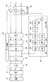
図1に、本実施形態におけるデジタルカメラの構成ブロック図を示す。レンズ10は、被写体からの光を撮像素子としてのCCD12に結像する。CCD12は、Bayer配列のカラーフィルタを有し、被写体光を光電変換して画像信号を生成してCDS14に供給する。CDS14は、CCD12からの画像信号を相関二重サンプリングしてアナログデジタル変換器A/D16に供給する。A/D16は、画像信号をデジタル信号に変換し、画像メモリ18に格納する。CCD12、CDS14及びA/D16はタイミングジェネレータ(TG)50から供給されるクロック信号に同期して動作し、画像メモリ18はメモリコントローラ12で読み出し及び書き込みが制御される。画像メモリ18から読み出された画像信号はRGB分離回路20にてR信号、G信号及びB信号に分離され、輝度色差信号生成回路22に供給される。輝度色差信号生成回路22は、R信号、G信号、B信号から輝度信号Y及び色差信号CR、CBを生成し、RGB信号生成回路24に供給する。RGB信号生成回路24は、輝度信号Y及び色差信号CR,CBから再びR信号、G信号、B信号を生成する。一度輝度信号及び色差信号に変換した後、再びRGB信号に戻す理由は、画像信号のエッジを検出するための輝度信号Yが必要となるからである。すなわち、輝度色差生成回路22で生成された輝度信号Yは、エッジ処理回路34に供給されてエッジが検出される。RGB信号生成回路24は、生成したR信号、G信号、B信号をホワイトバランス(WB)調整回路26に供給する。ホワイトバランス(WB)調整回路26は、R信号、G信号、B信号のホワイトバランスを調整して色補正回路28に供給する。また、ホワイトバランス調整回路26から出力されたR信号、G信号、B信号の少なくともいずれかは色にじみ検出回路(色収差検出回路)36に供給される。色補正回路28はR信号、G信号、B信号の色を補正してγ補正回路30に供給する。γ補正回路30はR信号、G信号、B信号にガンマ補正を施してRγ信号、Gγ信号、Bγ信号として輝度色差信号生成回路32に供給する。輝度色差信号生成回路32はガンマ補正された信号から輝度信号YL及び色差信号CR、CBを生成して出力する。輝度信号YLは加算回路35に供給され、色差信号CR、CBは色にじみ抑圧回路(色収差抑圧回路)38に供給される。加算回路35は、エッジ処理回路34でエッジ処理された輝度信号とガンマ補正された輝度信号とを加算し、画像メモリ40に格納する。また、色にじみ抑圧回路38は、後述するように色にじみ検出回路36で検出された色にじみ検出信号に基づいて色差信号に含まれる色収差を抑圧して画像メモリ40に格納する。画像メモリ40に格納された輝度信号及び色差信号は圧縮伸長回路42でJPEG等のフォーマットに圧縮され、あるいはRAWデータのままフラッシュメモリ等の記録媒体48に格納される。また、記録媒体48に格納された画像データは圧縮伸長回路42で伸長され、NTSC等の表示フォーマットに変換されてLCD46に表示される。画像メモリ40はメモリコントローラ12で読み出し及び書き込みが制御される。タイミングジェネレータ(TG)50、メモリコントローラ12、色にじみ検出回路36、圧縮伸長回路42はCPU44により制御され、CPU55はユーザ操作可能な操作部54からの操作信号に基づき制御する。
<First Embodiment>
FIG. 1 is a block diagram showing the configuration of a digital camera according to this embodiment. The
本実施形態の特徴の一つは、γ補正回路30でガンマ補正される前のR信号、G信号、B信号の少なくともいずれか、特にG信号をメイン信号として用いR信号及びB信号をサブ信号として用いて色にじみ(色収差)の発生を検出し、ガンマ補正された後の色差信号に対して色にじみを抑圧する処理を実行していることである。すなわち、色にじみを検出する回路をγ補正回路30の前段に配置するとともに、色にじみを抑圧する回路をγ補正回路30の後段に配置している。その理由は、γ補正回路30の前段において色にじみを抑圧してしまうと、その後のガンマ補正において色にじみを抑圧した部分がグレー化してしまい(色にじみを抑圧することで黒レベルとなるが、ガンマ補正によりこの黒レベルの輝度を補正してしまう)画質が変化して色にじみの抑圧効果が低減してしまうからである。
One of the features of this embodiment is that at least one of an R signal, a G signal, and a B signal before gamma correction is performed by the
以下、本実施形態における色にじみ検出回路(色収差検出回路)36と色にじみ抑圧回路(色収差抑圧回路)38について説明する。 Hereinafter, the color blur detection circuit (chromatic aberration detection circuit) 36 and the color blur suppression circuit (chromatic aberration suppression circuit) 38 according to this embodiment will be described.
図2に、色にじみ検出回路36の構成を示す。色にじみ検出回路36は、上記のとおり、γ補正回路30でガンマ補正する前のR信号、G信号、B信号を用いて色にじみの発生を検出し、その検出信号をγ補正回路30の後段に配置された色にじみ抑圧回路38に供給する。色にじみ検出回路36はγ補正回路30と並列に設けられ、ホワイトバランス調整回路26からのG信号を入力する。G信号を基準として色にじみを検出するのは、高輝度部分(ハイライト部分)におけるG信号に対するR信号あるいはB信号の分布が色にじみの主な原因だからである。なお、ハイライト以外の部分においても分布は生じるもののそのレベルは小さいため画質の点でほとんど問題とならない。
FIG. 2 shows the configuration of the color
色にじみ検出回路36は、ロースライス回路(LowSlice)36a、ハイパスフィルタ(HPF)36b、及びハイクリップ回路(HiClip)36cを有する。ロースライス回路36aは、ホワイトバランス調整回路26からのG信号のレベルを一定レベルでスライスし、ハイパスフィルタ36bに供給する。ハイパスフィルタ36bはロースライスされたG信号の高周波成分のみを抽出することで、G信号のハイライトのエッジを抽出する。ハイクリップ回路36cはハイパスフィルタ36bで抽出されたハイライトのエッジ信号から、上側の信号をクリップして(切り取って)下側の信号のみを抽出する。ハイクリップ回路36cで生成された信号はハイライトのエッジ部分を特定する信号であり、色にじみ検出信号として色にじみ抑圧回路38に供給される。
The color
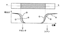
図3に、色にじみ検出回路36で生成される信号の信号波形を示す。図3(a)は被写体であるチャート100のラインab上のG信号とB信号のレベルを示す。上記のとおり、軸上収差及び倍率色収差によりR,G,B各信号には分布の差が生じ、例えばG信号とB信号で大きな分布の差が生じる。このG信号とB信号の分布の差が色にじみ200となって現れる。図の場合、偽の紫色がエッジ部分に出現する。図3(b)はロースライス回路36bでG信号をスライスする際のスライスレベルを示す。ハイライトのエッジ部分を抽出するために、スライスレベルは一定値以上に設定される。図3(c)はハイパスフィルタ36bを通過した後の信号であり、上側ピーク信号と下側ピーク信号が出現する。上側ピークは色にじみ200の発生部分を正確に反映しておらず、下側ピークが色にじみ200の発生部分を正確に反映する。そこで、図3(d)に示すようにハイクリップ回路36cで上側ピークを切り取り(図中破線はクリップされたことを示す)、下側ピークのみを出力する。図3(d)の信号が色にじみ検出信号として色にじみ抑圧回路38に供給される。
FIG. 3 shows a signal waveform of a signal generated by the color
一方、色にじみ抑圧回路38は、図2に示すように、乗算回路38a及び38bを有する。乗算回路38aは、輝度色差信号生成回路32からの色差信号CRと色にじみ検出回路36からの色にじみ検出信号との乗算を演算し、色にじみが発生している部分の色差信号CRを抑圧する。また、乗算回路38bは、輝度色差信号生成回路32からの色差信号CBと色にじみ検出回路36からの色にじみ検出信号との乗算を演算し、色にじみが発生している部分の色差信号CBを抑圧する。したがって、色にじみ検出回路36で検出された色にじみ部分では輝度信号のみが存在することとなり偽色が抑圧される。
On the other hand, the color
<第2実施形態>
図4に、本実施形態における色にじみ検出回路(色収差検出回路)36の構成を示す。図2に示された色にじみ検出回路36に対し、ハイクリップ回路36d及び乗算回路36eが付加された構成である。また、ホワイトバランス調整回路26からのG信号は図2と同様にロースライス回路36aに供給されるが、G信号はハイクリップ回路36dにも供給される。
<Second Embodiment>
FIG. 4 shows a configuration of a color blur detection circuit (chromatic aberration detection circuit) 36 in the present embodiment. In this configuration, a
ハイクリップ回路36dは、G信号のハイレベルをクリップして乗算回路36eに供給する。ハイクリップ回路36dでのクリップレベルはロースライス回路36aでのスライスレベルと同一である。乗算回路36eは、ハイクリップ回路36dでクリップされたG信号と、ハイクリップ回路36cからの信号(図3(d)参照)の乗算を演算する。
The
ハイライトのエッジ部分の色にじみを抑圧する際に、エッジであるもののG信号のレベルが十分低下しない場合がある。すなわち、ハイライト部分においてG信号は不連続的に低下するものの、低下後のレベルが未だ大きな値を維持する場合である。このような場合には色を抑圧することは好ましくないため、乗算回路36eでハイクリップ回路36dからの信号と乗算を演算することで色にじみ検出信号を出力させないようにする。本実施形態では、G信号のレベルが高いレベルから十分低いレベルまで低下するエッジ部分においてのみ色にじみ抑圧を実行すると云うことができる。
When suppressing the color blur at the edge portion of the highlight, the level of the G signal of the edge may not be sufficiently lowered. That is, although the G signal decreases discontinuously in the highlight portion, the level after the decrease still maintains a large value. In such a case, since it is not preferable to suppress the color, the
<第3実施形態>
図5に、本実施形態における色にじみ検出回路(色収差検出回路)36の構成を示す。図2に示された色にじみ検出回路36に対し、B信号を処理対象とするロースライス回路36f、ハイパスフィルタ36g、ロークリップ回路36h、反転回路36i及び乗算回路36eが付加された構成である。ホワイトバランス調整回路26からのG信号は図2と同様にロースライス回路36aに供給され、B信号はロースライス回路36fに供給される。
<Third Embodiment>
FIG. 5 shows a configuration of a color blur detection circuit (chromatic aberration detection circuit) 36 in the present embodiment. The color
ロースライス回路36f、ハイパスフィルタ36gはロースライス回路36a及びハイパスフィルタ36bと同様の機能を有し、入力した信号のハイライトのエッジ部分を抽出する。但し、ロースライス回路36f及びハイパスフィルタ36gはG信号ではなくB信号のハイライトのエッジ部分を抽出する。ハイパスフィルタ36gは、抽出した信号をロークリップ回路36hに供給する。ロークリップ回路36hは、入力信号の下側ピークをクリップして(切り取って)反転回路36iに供給する。ロークリップ回路36hは、ハイクリップ回路36cのクリップ極性(ハイレベル側)とは異なる極性(ローレベル側)でクリップする。反転回路36iは入力信号を反転して乗算回路36eに供給する。乗算回路36eは、ハイクリップ回路36cからの信号と反転回路36iからの信号の乗算を演算し、色にじみ検出信号として色にじみ抑圧回路38に供給する。
The
図6に、色にじみ検出回路の各部の信号波形を示す。図6(a)、(b)は図3(a)、(b)と同一の信号波形であり、G信号とB信号の波形である。G信号とB信号の分布差が色にじみ200となって現れる。ロースライス回路36aはG信号を所定のスライスレベルでロースライスする。また、ロースライス回路36fもB信号を同一のスライスレベルでロースライスする。図6(c)はハイパスフィルタ36bからの信号波形であり、ハイクリップ回路36cではこの信号の上側ピークを所定のクリップレベルでクリップし、下側のピークだけを抽出する。
FIG. 6 shows signal waveforms at various parts of the color blur detection circuit. FIGS. 6A and 6B are the same signal waveforms as FIGS. 3A and 3B, and are the waveforms of the G signal and the B signal. A difference in distribution between the G signal and the B signal appears as a
一方、図6(d)はハイパスフィルタ36gからの信号波形であり、ロークリップ回路36hではこの信号の下側ピークを所定のクリップレベルでクリップし、上側のピークだけを抽出する。反転回路36iは、図6(d)に示す信号波形を反転し、乗算回路36eはこれら2つの信号の乗算を演算する。図6(e)は乗算回路36eからの信号波形であり、色にじみ検出信号として色にじみ抑圧回路38に供給される信号波形である。図6から明らかなように、本実施形態ではG信号から生成されたハイライトのエッジ部分と、B信号から生成されたハイライトのエッジ部分との重複部分を色にじみの発生部分として検出している。いわば、G信号のハイライトエッジとB信号のハイライトエッジとでサンドイッチされた部分を色にじみ発生部分として検出している。色にじみはG信号とB信号の分布差により生じるから、G信号とB信号とで色にじみ検出信号を生成することで、より正確に色にじみを抑圧することができる。
On the other hand, FIG. 6D shows a signal waveform from the high-
<第4実施形態>
図7に、本実施形態における色にじみ検出回路(色収差検出回路)36の構成を示す。図5に示す色にじみ検出回路36に対し、ハイパスフィルタ36b、36gのカットオフ周波数特性が変更され、絶対値回路(ABS)回路36j、ローパスフィルタ36kが付加された構成である。
<Fourth embodiment>
FIG. 7 shows a configuration of a color blur detection circuit (chromatic aberration detection circuit) 36 in the present embodiment. In contrast to the color
ハイパスフィルタ36bと36gはカットオフ周波数が異なり、ハイパスフィルタ36gはハイパスフィルタ36bよりも一層高周波成分のみを抽出する。ハイパスフィルタ36gはB信号のより急峻な信号部分を抽出することから、ハイパスフィルタ36bに比べて「細い」信号を抽出すると云うことができる。絶対値回路36jはハイパスフィルタ36gで抽出された信号の絶対値を検出するため、高周波信号のうち下側ピークが反転した信号波形が得られる。ローパスフィルタ36kは絶対値回路36jからの信号波形を滑らかに整形して反転回路36iに供給する。
The high-
図8に、本実施形態における色にじみ検出回路36の各部の信号波形を示す。図8(a)、(b)、(c)は図6(a)、(b)、(c)と同一である。図8(d)はハイパスフィルタ36gからの信号波形である。G信号のハイライトのエッジよりも狭いエッジを抽出している。絶対値回路36jは、この信号の下側ピークを上側ピークに反転させる機能を有する、図では、破線で反転の様子を示す。図8(e)はローパスフィルタ36kからの信号波形である。絶対値回路36jからの信号を滑らかにした波形となる。乗算回路36eは、ハイクリップ回路36cからの信号と、図8(e)の信号の反転信号との乗算を演算して色にじみ検出信号として出力する。
FIG. 8 shows signal waveforms at various parts of the color
本実施形態においても、第3実施形態と同様にG信号のハイライトのエッジとB信号のハイライトのエッジの重複部分を色にじみ発生部分として検出しているが、本実施形態ではB信号のハイライトのエッジをより正確に検出することができる。 In the present embodiment as well, as in the third embodiment, the overlapping portion of the highlight edge of the G signal and the highlight edge of the B signal is detected as the color blur occurrence portion. Highlight edges can be detected more accurately.
<第5実施形態>
図9に、本実施形態における色にじみ検出回路(色収差検出回路)36の構成を示す。上記の各実施形態では、基本的にハイライトのエッジ部分を色にじみ発生部分として検出しているが、本実施形態では、ハイライトのエッジ部分であって特定の色域のみを色にじみ(色収差)として検出する構成を示す。
<Fifth Embodiment>
FIG. 9 shows a configuration of a color blur detection circuit (chromatic aberration detection circuit) 36 in the present embodiment. In each of the above-described embodiments, the highlight edge portion is basically detected as a color blur occurrence portion. However, in this embodiment, only a specific color gamut (color aberration) is a highlight edge portion. ) Shows the configuration to be detected.
図9において、色にじみ検出回路36は、図2と同様にロースライス回路36a、ハイパスフィルタ36b、ハイクリップ回路36cを有し、さらに、色差信号生成回路36m、演算回路36n、36q、ロークリップ回路36p、36r、乗算回路36s、36eを有する。ロースライス回路36a等は図2と同様にG信号のハイライトのエッジ部分を抽出する。
9, the color
色差信号生成回路36mは、ホワイトバランス調整回路26からのR信号、G信号、B信号から色差信号CR,CBを生成し、演算回路36n、36qに供給する。演算回路36nは、CB’=CB−k・CRの演算を行い、演算結果CB’をロークリップ回路36pに供給する。ロークリップ回路36pは入力信号CB’のローレベルをクリップし、CB’が正となる信号を出力する。すなわち、CB’>0を満たす信号である。一方、演算回路36qは、CR’=CR−m・CBの演算を行い、演算結果CR’をロークリップ回路36rに供給する。ロークリップ回路36rもロークリップ回路36pと同様に入力信号CR’のローレベルをクリップし、CR’が正となる信号を出力する。すなわち、CR’>0を満たす信号である。ここに、k及びmは所定のパラメータである。乗算回路36sは、2つの信号の乗算を演算して乗算回路36eに供給する。したがって、乗算回路36sからは、CB’>0であり、かつ、CR’>0である信号が出力され、反転回路36αで反転されて乗算回路36eに供給される。乗算回路36eではハイクリップ回路36cからの信号のうち、上記の条件を満たす信号のみが色にじみ検出信号として色にじみ抑圧回路38に供給される。
The color difference
図10に、本実施形態における色にじみ検出信号として出力される色域を示す。CB及びCRからなる色差空間において、CB−k・CR>0で規定される色域と、CR−m・CB>0で規定される色域との重複領域(図中斜線で示す領域)が色にじみとして抑圧される対象の色域である。図10の色域はマゼンタ領域に相当する。パラメータk、mを調整することで当該色域を種々変化させることができる。パラメータk、mは、予めデジタルカメラに用いられる撮影光学系の特性に応じて決定してシステムメモリに格納しておくことができる。また、撮影光学系の特性を計測し、システムメモリに予め格納されたデフォルトの値を計測値に応じて変更することで自動調整してもよい。さらに、ユーザが操作部54を操作することでパラメータk、mの値を手動調整してもよい。この場合、色にじみとして抑圧すべき特定の色域をユーザが選択できることになる。
FIG. 10 shows a color gamut output as a color blur detection signal in the present embodiment. In the color difference space consisting of CB and CR, there is an overlapping area (area shown by hatching in the figure) of the color gamut defined by CB-k · CR> 0 and the color gamut defined by CR-m · CB> 0. This is the target color gamut to be suppressed by color blur. The color gamut in FIG. 10 corresponds to a magenta area. The color gamut can be changed variously by adjusting the parameters k and m. The parameters k and m can be determined in advance according to the characteristics of the photographing optical system used in the digital camera and stored in the system memory. Alternatively, the characteristics of the photographic optical system may be measured and automatically adjusted by changing a default value stored in advance in the system memory in accordance with the measured value. Furthermore, the user may manually adjust the values of the parameters k and m by operating the
<第6実施形態>
図11に、本実施形態における色にじみ検出回路(色収差検出回路)36の構成を示す。図9に示された色にじみ検出回路36に対し、ハイクリップ回路36cの後段にローパスフィルタ36t及び乗算回路36vが付加されるとともに、ロースライス回路36aと並列にハイクリップ回路36uが付加された構成である。ハイクリップ回路36u及び乗算回路36vは、図4に示された第2実施形態の構成と同様の機能を有し、ハイライトのエッジでG信号レベルが十分低下した場合にのみ色にじみ検出信号を生成する。ローパスフィルタ36tはハイクリップ回路36cからの信号を滑らかにするためのもので、図4と同様になくてもよい。
<Sixth Embodiment>
FIG. 11 shows a configuration of a color blur detection circuit (chromatic aberration detection circuit) 36 in the present embodiment. The color
<第7実施形態>
図12に、本実施形態における色にじみ検出回路(色収差検出回路)36の構成を示す。図9に示された色にじみ検出回路36に対し、ローパスフィルタ36w、ロークリップ回路36x、反転回路36y、36α、及び乗算回路36zが付加された構成である。図9に示された色にじみ検出回路36では、特定の色域を検出対象としているが、本実施形態では、特定の色域であり、かつ、当該色域の幅が所定値以下の細い領域のみを検出対象とする。これは、当該色域の幅が所定値以上と太い、つまり連続して存在する場合には本来的に撮影画像に存在する色域であって偽色ではないとみなせるからであり、これを色にじみ抑圧の対象から除外するためである。
<Seventh embodiment>
FIG. 12 shows a configuration of a color blur detection circuit (chromatic aberration detection circuit) 36 in the present embodiment. In this configuration, a low-
乗算回路36sからの信号は2つに分岐され、一方は乗算回路36zに供給され、他方はローパスフィルタ36w、ロークリップ回路36x及び反転回路36yに供給される。反転回路36yからの信号は乗算回路36zに供給され、2つの信号の乗算が演算される。乗算回路36zからの信号は反転回路36αで反転されて乗算回路36eに供給される。すなわち、乗算回路36sからの信号のうち、ローパスフィルタ36w等で処理された信号成分を含む信号のみが色にじみ検出信号として色にじみ抑圧回路38に供給されることになる。
The signal from the
図13に、特定色域信号の幅(細い場合と太い連続した場合)が異なる場合の、ローパスフィルタ36w、ロークリップ回路36x、反転回路36y及び乗算回路36zの各部の信号波形を示す。図13(a)は乗算回路36sからの信号波形であり、信号幅が細い場合と太い連続した場合とを対比して示す。特定色域をマゼンタとした場合、マゼンタの信号波形とみなすことができる。図13(b)はローパスフィルタ36wからの信号波形である。図13(c)はロークリップ回路36xのクリップレベルを示す。細い場合にはクリップレベルよりも入力信号レベルは低くなる。また、太く連続した場合にはクリップレベルよりも上の部分がクリップされる。図13(d)は反転回路36yからの信号波形を示す。細い場合には一定のレベルとなり(ゼロレベル信号を反転した信号)、太い連続した信号はクリップした信号の反転波形となる。図13(e)は乗算回路36zからの信号波形を示す。図13(a)の信号と図13(d)の信号の乗算で得られる信号波形である。細い場合にはピークレベル信号が得られるが、太く連続した場合にはレベルの小さい信号となる。図13(e)に示す信号は反転回路26αで反転されて乗算回路36eに供給されるから、結果として細い場合には色にじみ検出信号として出力され、太い連続した場合には色にじみ検出信号が出力されず(色にじみを示す値が出力されない)、色にじみ抑圧回路38で色差信号の抑圧は実行されないことになる。
FIG. 13 shows signal waveforms at various parts of the low-
このように、本実施形態では特定色域信号の信号幅が所定値以下となる場合のみ色にじみを抑圧することで、不必要に色を除去してしまう事態を防止することができる。検出対象とする信号幅は、ロークリップ回路36xのクリップレベルで増減調整できる。
As described above, in this embodiment, it is possible to prevent a situation where the color is unnecessarily removed by suppressing the color blur only when the signal width of the specific color gamut signal is equal to or smaller than the predetermined value. The signal width to be detected can be increased or decreased by the clip level of the
<第8実施形態>
図14に、本実施形態における色にじみ検出回路(色収差検出回路)36の構成を示す。図12と同様に特定の色域信号のうち信号幅が所定値以下の信号のみを検出する場合である。図12の色にじみ検出回路36に対し、ローパスフィルタ36wをロークリップ回路36βで置き換え、ロークリップ回路36xをフィルタ36γで置き換えた構成である。ロークリップ回路36βは、乗算回路36sからの信号のローレベルをクリップし、フィルタ36γに供給する。フィルタ36γはローパスフィルタであり、高周波成分を除去して反転回路36yに供給する。
<Eighth Embodiment>
FIG. 14 shows a configuration of a color blur detection circuit (chromatic aberration detection circuit) 36 in the present embodiment. In the same manner as in FIG. 12, only signals having a signal width of a predetermined value or less are detected from specific color gamut signals. In contrast to the color
図15に、図14の各部の信号波形を示す。信号幅が細い場合と太い連続した場合とを対比して示す。図15(a)はロークリップ回路36βのクリップレベルを示す。クリップレベルよりも下のレベルがクリップされる(切り取られる)。図15(b)はフィルタ36γからの信号波形であり、細い場合はロークリップ回路36βの処理により残存した信号が除去される。図15(c)は反転回路36yからの信号波形であり、図15(d)は乗算回路36zからの信号波形、すなわち図15(a)の信号波形と図15(c)の信号波形の乗算である。細い場合にはピーク信号が得られるが、太い連続した場合にはレベルの小さい信号となり、太い連続した場合には色にじみ検出信号が出力されず(色にじみを示す値が出力されない)、色にじみ抑圧回路38で色差信号の抑圧は実行されない。
FIG. 15 shows signal waveforms at various parts in FIG. The case where the signal width is narrow and the case where the signal width is continuous are shown in comparison. FIG. 15A shows the clip level of the low clip circuit 36β. The level below the clip level is clipped (cut). FIG. 15B shows a signal waveform from the filter 36γ. When the signal waveform is thin, the remaining signal is removed by the processing of the low clip circuit 36β. FIG. 15C shows a signal waveform from the inverting
<第9実施形態>
図16に、本実施形態における色にじみ検出回路(色収差検出回路)36の構成を示す。図11に示す色にじみ検出回路36における構成を多重化したものである。より特定邸には、図11ではマゼンタの色域を抑圧しているが、本実施形態ではマゼンタの色域とシアンの色域を抑圧する。すなわち、ロースライス回路36a1、ハイパスフィルタ36b1、ハイクリップ回路36c1、ローパスフィルタ36t1、ハイクリップ回路36u1、色差信号生成回路36m、演算回路36n1、36q1、ロークリップ回路36p1、36r1、乗算回路36s1、36e1、36v1は図11の構成と同一であり、さらに、ロースライス回路36a2、ハイパスフィルタ36b2、ハイクリップ回路36c2、ローパスフィルタ36t2、ロークリップ回路36u2、演算回路36n2、36q2、ロークリップ回路36p2、36r2、乗算回路36s2、36e2、36v2及び最大値回路(MAX)36δが付加された構成である。
<Ninth Embodiment>
FIG. 16 shows a configuration of a color blur detection circuit (chromatic aberration detection circuit) 36 in the present embodiment. The configuration in the color
ロースライス回路36a2、ハイパスフィルタ36b2、ハイクリップ回路36c2、ローパスフィルタ36t2、ロークリップ回路36u2、ロークリップ回路36p2、36r2、乗算回路36s2、36e2、36v2はそれぞれロースライス回路36a1、ハイパスフィルタ36b1、ハイクリップ回路36c1、ローパスフィルタ36t1、ハイクリップ回路36u1、ロークリップ回路36p1、36r1、乗算回路36s1、36e1、36v1と基本的に同一の機能を有する。但し、ロークリップ回路36u2はハイクリップ回路36u1と異なり、G信号のハイレベルをクリップする。その理由は、演算回路36n2等はシアンの色域を特定するが、図17の被写体チャート及びこれを撮影したときのR信号、G信号、B信号のレベル分布から分かるように、シアンはハイライトのエッジ部分における高輝度側に生じるからである。これに対し、マゼンタはハイライトのエッジ部分における低輝度側に生じるからハイクリップ回路36u1ではハイレベルをクリップしている。また、ロースライス回路36a2にはG信号ではなくR信号が供給され、R信号のハイライトのエッジ部分を抽出する。G信号ではなくR信号を用いるのは、図17に示されるようにシアンはB信号とR信号の分布差により生じるからであり、R信号のハイライトのエッジ部分に生じるからである。 The low slice circuit 36a2, the high pass filter 36b2, the high clip circuit 36c2, the low pass filter 36t2, the low clip circuit 36u2, the low clip circuits 36p2, 36r2, and the multiplier circuits 36s2, 36e2, 36v2 are respectively a low slice circuit 36a1, a high pass filter 36b1, and a high clip. The circuit 36c1, the low-pass filter 36t1, the high clip circuit 36u1, the low clip circuits 36p1 and 36r1, and the multiplier circuits 36s1, 36e1, and 36v1 have basically the same functions. However, unlike the high clip circuit 36u1, the low clip circuit 36u2 clips the high level of the G signal. The reason is that the arithmetic circuit 36n2 and the like specify the cyan color gamut, but as shown in the subject chart of FIG. 17 and the level distribution of the R signal, G signal, and B signal when this is taken, cyan is highlighted. This is because it occurs on the high-luminance side of the edge portion. On the other hand, since magenta occurs on the low luminance side in the edge portion of the highlight, the high clipping circuit 36u1 clips the high level. The low slice circuit 36a2 is supplied with the R signal instead of the G signal, and extracts the highlight edge portion of the R signal. The reason why the R signal is used instead of the G signal is that cyan is caused by the distribution difference between the B signal and the R signal as shown in FIG. 17, and is generated at the edge portion of the highlight of the R signal.
乗算回路36e1は、図11と同様にハイクリップ回路36c1からの信号のうち、CB’>0であり、かつ、CR’>0である信号が最大値回路36δに供給される。一方、演算回路36n2、36q2は、CB’’=c・CB−CRの演算を行い、演算結果CB’’をロークリップ回路36p2に供給する。ロークリップ回路36p2は入力信号CB’’のローレベルをクリップし、CB’が正となる信号を出力する。すなわち、CB’’>0を満たす信号である。また、演算回路36q2は、CR’’=d・CR−CBの演算を行い、演算結果CR’’をロークリップ回路36r2に供給する。ロークリップ回路36r2もロークリップ回路36p2と同様に入力信号CR’’のローレベルをクリップし、CR’’が正となる信号を出力する。すなわち、CR’’>0を満たす信号である。ここに、c及びdは所定のパラメータである。乗算回路36s2は、2つの信号の乗算を演算して乗算回路36e2に供給する。したがって、乗算回路36s2からは、CB’’<0であり、かつ、CR’’>0となる信号が出力され、乗算回路36e2ではハイクリップ回路36c2からの信号のうち、上記の条件を満たす信号のみが最大値回路36δに供給される。最大値回路36δは、いずれ大きい方の信号を選択して色にじみ検出信号として色にじみ抑圧回路38に供給する。
Similarly to FIG. 11, the multiplication circuit 36e1 supplies a signal satisfying CB ′> 0 and CR ′> 0 among the signals from the high clip circuit 36c1 to the maximum value circuit 36δ. On the other hand, the arithmetic circuits 36n2 and 36q2 perform an operation of CB ″ = c · CB-CR, and supply the operation result CB ″ to the low clip circuit 36p2. The low clip circuit 36p2 clips the low level of the input signal CB ″ and outputs a signal that makes CB ′ positive. That is, the signal satisfies CB ″> 0. The arithmetic circuit 36q2 performs an operation of CR ″ = d · CR−CB and supplies the operation result CR ″ to the low clip circuit 36r2. Similarly to the low clip circuit 36p2, the low clip circuit 36r2 clips the low level of the input signal CR ″ and outputs a signal in which CR ″ becomes positive. That is, the signal satisfies CR ″> 0. Here, c and d are predetermined parameters. The multiplication circuit 36s2 calculates the multiplication of the two signals and supplies it to the multiplication circuit 36e2. Therefore, a signal that satisfies CB ″ <0 and CR ″> 0 is output from the multiplication circuit 36s2, and the multiplication circuit 36e2 is a signal that satisfies the above conditions among the signals from the high clip circuit 36c2. Only the maximum value circuit 36δ is supplied. The maximum value circuit 36δ selects the larger signal and supplies it to the color
図18A及び図18Bに、本実施形態の演算回路36n1、36q1、36n2、36q2で特定される色域を示す。図18は演算回路36n1、36q1で特定される色域でありマゼンタに相当する、図18Bは演算回路36n2、36q2で特定される色域でありシアンに相当する。本実施形態では、ハイライトのエッジ部分の低輝度側に生じるマゼンタ、及びハイライトのエッジ部分の高輝度側に生じるシアンのうち、いずれかレベルの大きい方を抑圧することができる。もちろん、最大値回路36δを加算回路で置き換えてマゼンタ及びシアンをともに抑圧することもできる。 18A and 18B show color gamuts specified by the arithmetic circuits 36n1, 36q1, 36n2, and 36q2 of the present embodiment. FIG. 18 shows the color gamut specified by the arithmetic circuits 36n1 and 36q1 and corresponds to magenta. FIG. 18B shows the color gamut specified by the arithmetic circuits 36n2 and 36q2 and corresponds to cyan. In the present embodiment, the higher one of magenta generated on the low luminance side of the highlight edge portion and cyan generated on the high luminance side of the highlight edge portion can be suppressed. Of course, it is also possible to suppress both magenta and cyan by replacing the maximum value circuit 36δ with an adding circuit.
なお、図16の構成において、色差信号生成回路36m、演算回路36n2、36q2、ロークリップ回路36p2、36r2、乗算回路36s2、36e2、36v2、ロースライス回路36a2、ハイパスフィルタ36b2、ハイクリップ回路36c2、ローパスフィルタ36t2のみを有し、R信号、G信号、B信号から色差信号CB、CRを生成するとともに、R信号のハイライトのエッジを検出して、シアンに相当する色にじみを検出する構成とすることもできる。図11においてマゼンタの代わりにシアンを検出する構成に対応するものである。要するに、マゼンタの色にじみのみを検出する構成、シアンの色にじみのみを検出する構成、マゼンタ及びシアンの色にじみを検出する構成のいずれでもよい。
In the configuration of FIG. 16, the color difference
<第10実施形態>
図19に、本実施形態におけるデジタルカメラの構成を示す。図1に対し、色抑圧回路38がガンマ補正後ではなくガンマ補正前に配置されている点が異なる。第1実施形態で述べたように、ガンマ補正前で色にじみ(色収差)を抑圧してしまうと、ガンマ補正により色にじみを抑圧した部分がグレー化してしまう問題がある。そこで、本実施形態では、ガンマ補正前で色にじみを抑圧する際に、輝度信号も同時に補正することで、ガンマ補正によるグレー化を抑制する。
<Tenth Embodiment>
FIG. 19 shows the configuration of the digital camera in this embodiment. The difference from FIG. 1 is that the
図19において、色抑圧回路38は、ホワイトバランス調整回路26と色補正回路28との間に配置される。色抑圧回路38は、乗算回路38a、38b、38c、輝度色差信号生成回路38d及びRGB信号生成回路38eを有する。輝度色差信号生成回路38dは、ホワイトバランス調整回路26からのR信号、G信号、B信号から輝度信号Y及び色差信号CB,CRを生成して乗算回路38a、38b、38cに供給する。乗算回路38a、38bは図3における色抑圧回路38の乗算回路38a、38bと同様にそれぞれ色差信号CR、CBと色にじみ検出信号との乗算を演算して色差信号をゼロとする(つまり、R,G,Bのレベルを同一とする)。一方、乗算回路38cは、輝度信号と色にじみ検出信号との乗算を演算することで輝度信号を抑圧する。乗算回路38a、38b、38cはそれぞれ演算結果をRGB信号生成回路38eに供給する。RGB生成回路38eは輝度信号Y及び色差信号CB,CRから再びR信号、G信号、B信号を生成して色補正回路28に供給する。
In FIG. 19, the
なお、色にじみ検出回路36の構成は図3に示された色にじみ検出回路36と同一である。
The configuration of the color
このように、本実施形態では、色差信号CB,CRを補正して色にじみを抑圧すると同時に、輝度信号Yのレベルも補正するため、その後のγ補正回路30でガンマ補正された場合でも輝度は大きく増大せずグレー化することがない。
As described above, in this embodiment, the color difference signals CB and CR are corrected to suppress the color blur, and at the same time, the level of the luminance signal Y is also corrected. Therefore, even when the gamma correction is performed by the subsequent
図20に本実施形態の比較例を示す。図19と同様にガンマ補正の前に色にじみを抑圧する場合である。但し、色にじみ抑圧回路37は図19における色にじみ抑圧回路38と異なり、乗算回路38cを有しておらず、輝度信号Yを補正しない。この場合、色差信号CB、CRを補正することで色にじみを抑圧することが可能であるが、輝度信号YはそのままなのでR,G,Bのレベル自体はそのまま残存し、その後のガンマ補正でさらにそのレベルが増大するためグレー化してしまうことになる。
FIG. 20 shows a comparative example of this embodiment. As in FIG. 19, this is a case where color blur is suppressed before gamma correction. However, unlike the color
以上、本発明の実施形態について説明したが、本発明はこれらに限定されるものではなく、他の形態も可能である。例えば、図2の構成では色にじみ検出回路36はハイクリップ回路36cを有しているが、他の回路で置換することも可能である。図21には、他の色にじみ検出回路36の構成を示す。図2の構成に対し、ハイクリップ回路36cをハイクリップ及び反転回路36c’及び演算回路36d’で置換した構成である。ハイクリップ及び反転回路36c’は、ハイパスフィルタ36bからの信号をハイクリップし、さらに所定の変換テーブルを用いてハイクリップした信号を反転して出力する。演算回路36d’は、ハイクリップ及び反転回路36c’からの信号Sに対し、1−Sの演算を実行して色にじみ検出信号として色にじみ抑圧回路38に供給する。
As mentioned above, although embodiment of this invention was described, this invention is not limited to these, Other forms are also possible. For example, in the configuration of FIG. 2, the color
図22に、図21の構成の信号波形を示す。図3に対応するものである。図22(d)はハイクリップ及び反転回路36c’からの信号波形である。ハイクリップ及び反転回路36c’は、図22(c)に示すように2つのクリップレベルでそれぞれハイクリップ及びロークリップを実行した後、反転する。クリップと反転とを所定の重み関数を用いて同時に実行することも可能である。図23に、クリップと反転とを同時に実行するための重み関数を示す。図23において、横軸は入力レベル、縦軸は出力レベルである。入力レベルが負の一定レベルまでは重み「1」を出力し、入力レベル0までは徐々に出力レベルは小さくなり、入力レベルが0のときに出力レベルは0となり、入力レベルが正であれば出力レベルは0となるような関数である。図23から、ハイクリップ、ロークリップ及び反転が同時に実行されることが理解されよう。図22(e)は演算回路36d’からの信号波形であり、図22(d)の信号波形(この信号をSとする)に対し、1−Sの信号波形である。図22(e)の信号が色にじみ抑圧回路38に供給されて色差信号に含まれる色にじみを抑圧する。すなわち、図22(e)の信号におけるレベル0の部分で色差が除去されて偽色が除去される。図4、図5、図7、図9、図11、図12、図14、図19におけるハイクリップ回路36c、及び図16におけるハイクリップ回路36c1、36c2についても同様にハイクリップ及び反転回路36c’と演算回路36d’に置換することができる。
FIG. 22 shows signal waveforms of the configuration of FIG. This corresponds to FIG. FIG. 22D shows a signal waveform from the high clip and
また、図11の構成では、ハイクリップ回路36uにはG信号が供給されるものとしたが、図24に示すように、色差信号生成回路36mを輝度色差信号生成回路36m’に置換し、生成した輝度信号Yをハイクリップ回路36uに供給してもよい。ハイクリップ回路36uは輝度信号Yをハイクリップして乗算回路36vに供給する。
In the configuration shown in FIG. 11, the G signal is supplied to the
以上、本発明の実施形態について、デジタルカメラを例にとり説明した。しかしながら、本発明はデジタルカメラ等の撮像装置のみに適用されるものではなく、例えばコンピュータにインストールされる画像処理プログラムに組み込むことも可能である。画像処理プログラムに上記の各実施形態で実行される処理をサブルーチンプログラムとして組み込む。一方、被写体画像は入力装置から入力されてメモリに記憶される。コンピュータのCPUは該プログラムを補助記憶装置から主記憶装置にロードし、被写体画像をメモリから読み出し、該プログラムを順次実行することで被写体画像のハイライトのエッジ部分に生じている色にじみ(色収差)を検出し、その部分の色にじみを抑圧して液晶ディスプレイなどの表示装置に表示する。入力画像信号に対して図3におけるロースライス処理、ハイパスフィルタ処理、ハイクリップ処理、乗算演算処理等の各処理をコンピュータ上で実行する技術は周知である。 The embodiment of the present invention has been described above by taking the digital camera as an example. However, the present invention is not applied only to an imaging apparatus such as a digital camera, and can be incorporated into an image processing program installed in a computer, for example. The processing executed in each of the above embodiments is incorporated into the image processing program as a subroutine program. On the other hand, the subject image is input from the input device and stored in the memory. The CPU of the computer loads the program from the auxiliary storage device to the main storage device, reads out the subject image from the memory, and sequentially executes the program to cause color blur (chromatic aberration) occurring at the highlight edge portion of the subject image. Is detected and the color blur of the portion is suppressed and displayed on a display device such as a liquid crystal display. A technique for executing, on a computer, each process such as a low slice process, a high pass filter process, a high clip process, and a multiplication operation process in FIG. 3 for an input image signal.
10 レンズ、12 CCD,14 CDS、16 A/D、18 画像メモリ、20 RGB分離回路、22 輝度色差信号生成回路、24 RGB信号生成回路、26 ホワイトバランス調整回路、28 色補正回路、30 γ補正回路、32 輝度色差信号生成回路、34 エッジ処理回路、35 加算回路、36 色にじみ検出回路(色収差検出回路)、38 色にじみ抑圧回路(色収差抑圧回路)、40 画像メモリ、42 圧縮伸長回路、44 CPU、46 LCD、48 記憶媒体、50 タイミングジェネレータ、52 メモリコントローラ、54 操作部。 10 lens, 12 CCD, 14 CDS, 16 A / D, 18 image memory, 20 RGB separation circuit, 22 luminance color difference signal generation circuit, 24 RGB signal generation circuit, 26 white balance adjustment circuit, 28 color correction circuit, 30 γ correction Circuit, 32 luminance color difference signal generation circuit, 34 edge processing circuit, 35 addition circuit, 36 color blur detection circuit (chromatic aberration detection circuit), 38 color blur suppression circuit (chromatic aberration suppression circuit), 40 image memory, 42 compression / decompression circuit, 44 CPU, 46 LCD, 48 storage medium, 50 timing generator, 52 memory controller, 54 operation unit.
Claims (4)
検出回路により被写体画像のガンマ補正前の画像信号から色収差部分を検出するステップと、
前記画像信号をガンマ補正するステップと、
ガンマ補正された画像信号に対し、検出された前記色収差部分の色成分を抑圧して表示装置に表示するステップと、
を実行するものであり、
前記検出回路は、
ガンマ補正前の画像信号を所定レベルでスライスするスライス回路と、
前記スライス回路でスライスされた画像信号の高周波成分を抽出するハイパスフィルタと、
前記ハイパスフィルタの出力信号を第2所定レベルでクリップするクリップ回路と、
を備えることを特徴とする色収差抑圧プログラム。 A program for suppressing chromatic aberration of a subject image, the program being installed in a computer,
Detecting a chromatic aberration portion from an image signal before gamma correction of a subject image by a detection circuit;
Gamma correcting the image signal;
A step of suppressing the detected color component of the chromatic aberration portion and displaying the image signal on the display device for the gamma corrected image signal;
Is to execute
The detection circuit includes:
A slice circuit that slices the image signal before gamma correction at a predetermined level;
A high-pass filter that extracts a high-frequency component of the image signal sliced by the slice circuit;
A clipping circuit that clips the output signal of the high-pass filter at a second predetermined level;
A chromatic aberration suppression program comprising:
前記被写体像のガンマ補正前の画像信号から色収差部分を検出する検出手段と、 Detecting means for detecting a chromatic aberration portion from an image signal before gamma correction of the subject image;
前記画像信号をガンマ補正するガンマ補正手段と、 Gamma correction means for gamma correcting the image signal;
前記ガンマ補正手段でガンマ補正された画像信号に対し、前記検出手段で検出された色収差部分の色成分を抑圧する抑圧手段と、 Suppression means for suppressing the color component of the chromatic aberration portion detected by the detection means for the image signal that has been gamma corrected by the gamma correction means;
を有し、 Have
前記検出手段は、 The detection means includes
前記ガンマ補正前の画像信号を第1所定レベルでスライスするスライス回路と、A slice circuit that slices the image signal before the gamma correction at a first predetermined level;
前記スライス回路でスライスされた画像信号の高周波成分を抽出するハイパスフィルタと、 A high-pass filter that extracts a high-frequency component of the image signal sliced by the slice circuit;
前記ハイパスフィルタからの信号を第2所定レベルでクリップするクリップ回路と、 A clipping circuit that clips the signal from the high-pass filter at a second predetermined level;
を備えることを特徴とする色収差抑圧回路。 A chromatic aberration suppression circuit comprising:
前記検出手段は、さらに、 The detection means further includes
前記ガンマ補正前の画像信号を前記第1所定レベルでクリップする第2クリップ回路と、 A second clipping circuit for clipping the image signal before the gamma correction at the first predetermined level;
前記クリップ回路からの信号と、前記第2クリップ回路からの信号の乗算を演算する乗算回路と、 A multiplication circuit for calculating multiplication of a signal from the clip circuit and a signal from the second clip circuit;
を備えることを特徴とする色収差抑圧回路。 A chromatic aberration suppression circuit comprising:
前記検出手段は、さらに、
前記ガンマ補正前の画像信号から高輝度部分のエッジを検出するエッジ検出手段
を有することを特徴とする色収差抑圧回路。 The chromatic aberration suppressing circuit according to claim 2,
The detection means further includes
Edge detection means for detecting an edge of a high brightness portion from the image signal before gamma correction
Chromatic aberration suppression circuit and having a.
Priority Applications (2)
| Application Number | Priority Date | Filing Date | Title |
|---|---|---|---|
| JP2005318847A JP4469324B2 (en) | 2005-11-01 | 2005-11-01 | Chromatic aberration suppression circuit and chromatic aberration suppression program |
| US11/423,770 US7583301B2 (en) | 2005-11-01 | 2006-06-13 | Imaging device having chromatic aberration suppression |
Applications Claiming Priority (1)
| Application Number | Priority Date | Filing Date | Title |
|---|---|---|---|
| JP2005318847A JP4469324B2 (en) | 2005-11-01 | 2005-11-01 | Chromatic aberration suppression circuit and chromatic aberration suppression program |
Publications (3)
| Publication Number | Publication Date |
|---|---|
| JP2007129361A JP2007129361A (en) | 2007-05-24 |
| JP2007129361A5 JP2007129361A5 (en) | 2008-12-11 |
| JP4469324B2 true JP4469324B2 (en) | 2010-05-26 |
Family
ID=37995767
Family Applications (1)
| Application Number | Title | Priority Date | Filing Date |
|---|---|---|---|
| JP2005318847A Expired - Fee Related JP4469324B2 (en) | 2005-11-01 | 2005-11-01 | Chromatic aberration suppression circuit and chromatic aberration suppression program |
Country Status (2)
| Country | Link |
|---|---|
| US (1) | US7583301B2 (en) |
| JP (1) | JP4469324B2 (en) |
Families Citing this family (41)
| Publication number | Priority date | Publication date | Assignee | Title |
|---|---|---|---|---|
| JP4712631B2 (en) * | 2005-07-28 | 2011-06-29 | 京セラ株式会社 | Imaging device |
| JP4487903B2 (en) * | 2005-11-09 | 2010-06-23 | ソニー株式会社 | Image processing apparatus and method, and program |
| JP2007322560A (en) * | 2006-05-30 | 2007-12-13 | Kyocera Corp | Imaging apparatus, and apparatus and method of manufacturing the same |
| JP4749959B2 (en) * | 2006-07-05 | 2011-08-17 | 京セラ株式会社 | Imaging device, manufacturing apparatus and manufacturing method thereof |
| JP2008048293A (en) * | 2006-08-18 | 2008-02-28 | Kyocera Corp | Imaging device and method for manufacturing same |
| JP2008053800A (en) * | 2006-08-22 | 2008-03-06 | Pentax Corp | Digital camera |
| JP4749984B2 (en) * | 2006-09-25 | 2011-08-17 | 京セラ株式会社 | Imaging device, manufacturing apparatus and manufacturing method thereof |
| JP4749985B2 (en) * | 2006-09-28 | 2011-08-17 | 京セラ株式会社 | Imaging device, manufacturing apparatus and manufacturing method thereof |
| US8144984B2 (en) * | 2006-12-08 | 2012-03-27 | Canon Kabushiki Kaisha | Image processing apparatus, image processing method, and program for color fringing estimation and compensation |
| JP4290193B2 (en) * | 2006-12-26 | 2009-07-01 | 三洋電機株式会社 | Image processing device |
| WO2008081903A1 (en) * | 2006-12-27 | 2008-07-10 | Kyocera Corporation | Imaging device and information code reading device |
| KR100866490B1 (en) * | 2007-01-17 | 2008-11-03 | 삼성전자주식회사 | Apparatus and method for compensating chromatic aberration of image |
| US8567678B2 (en) * | 2007-01-30 | 2013-10-29 | Kyocera Corporation | Imaging device, method of production of imaging device, and information code-reading device |
| JP2009010730A (en) * | 2007-06-28 | 2009-01-15 | Kyocera Corp | Image processing method and imaging apparatus employing the same |
| JP4844979B2 (en) * | 2007-08-30 | 2011-12-28 | 京セラ株式会社 | Image processing method and imaging apparatus using the image processing method |
| JP4992698B2 (en) * | 2007-12-17 | 2012-08-08 | ソニー株式会社 | Chromatic aberration correction apparatus, imaging apparatus, chromatic aberration calculation method, and chromatic aberration calculation program |
| JP5121498B2 (en) * | 2008-02-25 | 2013-01-16 | キヤノン株式会社 | Imaging apparatus and image data correction method |
| JP5078147B2 (en) * | 2008-03-04 | 2012-11-21 | 株式会社リコー | Image processing apparatus and image pickup apparatus |
| US8363129B2 (en) * | 2008-06-27 | 2013-01-29 | Kyocera Corporation | Imaging device with aberration control and method therefor |
| JP4658162B2 (en) * | 2008-06-27 | 2011-03-23 | 京セラ株式会社 | Imaging apparatus and electronic apparatus |
| US8502877B2 (en) * | 2008-08-28 | 2013-08-06 | Kyocera Corporation | Image pickup apparatus electronic device and image aberration control method |
| JP5178421B2 (en) * | 2008-09-12 | 2013-04-10 | キヤノン株式会社 | Image processing apparatus, image processing method, and imaging apparatus |
| JP4743553B2 (en) * | 2008-09-29 | 2011-08-10 | 京セラ株式会社 | Lens unit, imaging device, and electronic device |
| JP5183453B2 (en) * | 2008-12-17 | 2013-04-17 | キヤノン株式会社 | Image processing apparatus, image processing method, and program |
| JP5486273B2 (en) * | 2008-12-26 | 2014-05-07 | キヤノン株式会社 | Image processing apparatus and image processing method |
| JP5523141B2 (en) * | 2009-05-28 | 2014-06-18 | キヤノン株式会社 | Image processing apparatus, image processing method, and program |
| JP2010288150A (en) * | 2009-06-12 | 2010-12-24 | Toshiba Corp | Solid-state imaging device |
| JP2011041094A (en) * | 2009-08-14 | 2011-02-24 | Canon Inc | Image processing apparatus, imaging apparatus, and method of processing image |
| TWI394434B (en) * | 2009-12-30 | 2013-04-21 | Altek Corp | The method of eliminating the color dislocation of digital images |
| TWI395468B (en) * | 2009-12-30 | 2013-05-01 | Altek Corp | The method of eliminating the color dislocation of digital images |
| JP5589660B2 (en) * | 2010-08-12 | 2014-09-17 | 株式会社ニコン | Image processing apparatus, imaging apparatus, and image processing program |
| US8553978B2 (en) | 2010-11-03 | 2013-10-08 | Csr Technology Inc. | System and method for providing multi resolution purple fringing detection and correction |
| CN102158730B (en) * | 2011-05-26 | 2014-04-02 | 威盛电子股份有限公司 | Image processing system and method |
| CN102158731B (en) * | 2011-05-26 | 2014-03-12 | 威盛电子股份有限公司 | Image processing system and method |
| KR20140086632A (en) * | 2012-12-28 | 2014-07-08 | 삼성디스플레이 주식회사 | Image processing device and display device having them |
| JP6354134B2 (en) * | 2013-10-30 | 2018-07-11 | リコーイメージング株式会社 | Image processing apparatus, imaging apparatus, image processing method, and image processing program |
| JP6337441B2 (en) * | 2013-10-30 | 2018-06-06 | リコーイメージング株式会社 | Image processing apparatus, imaging apparatus, image processing method, and image processing program |
| JP6318549B2 (en) * | 2013-10-30 | 2018-05-09 | リコーイメージング株式会社 | Image processing apparatus, imaging apparatus, image processing method, and image processing program |
| US9674466B2 (en) * | 2015-02-26 | 2017-06-06 | Dual Aperture International Co., Ltd. | Hybrid image correction for dual-aperture camera |
| JP2018121239A (en) * | 2017-01-26 | 2018-08-02 | 株式会社日立国際電気 | Imaging apparatus and imaging method |
| JP6974156B2 (en) * | 2017-12-19 | 2021-12-01 | オリンパス株式会社 | Image color conversion device, image color conversion program, image color conversion method |
Family Cites Families (6)
| Publication number | Priority date | Publication date | Assignee | Title |
|---|---|---|---|---|
| JP3382973B2 (en) * | 1992-02-07 | 2003-03-04 | オリンパス光学工業株式会社 | Electronic endoscope device |
| JP2003060983A (en) | 2001-08-10 | 2003-02-28 | Olympus Optical Co Ltd | Imaging device |
| JP4010254B2 (en) * | 2003-02-06 | 2007-11-21 | ソニー株式会社 | Image recording / reproducing apparatus, image photographing apparatus, and chromatic aberration correction method |
| US6782217B1 (en) * | 2003-02-14 | 2004-08-24 | Kyocera Mita Corporation | Image forming device which detects and processes control data on original document |
| JP4250506B2 (en) | 2003-10-31 | 2009-04-08 | キヤノン株式会社 | Image processing method, image processing apparatus, image processing program, and imaging system |
| JP4706635B2 (en) * | 2004-04-12 | 2011-06-22 | 株式会社ニコン | Image processing apparatus having color misregistration correction function, image processing program, and electronic camera |
-
2005
- 2005-11-01 JP JP2005318847A patent/JP4469324B2/en not_active Expired - Fee Related
-
2006
- 2006-06-13 US US11/423,770 patent/US7583301B2/en not_active Expired - Fee Related
Also Published As
| Publication number | Publication date |
|---|---|
| US7583301B2 (en) | 2009-09-01 |
| US20070097267A1 (en) | 2007-05-03 |
| JP2007129361A (en) | 2007-05-24 |
Similar Documents
| Publication | Publication Date | Title |
|---|---|---|
| JP4469324B2 (en) | Chromatic aberration suppression circuit and chromatic aberration suppression program | |
| EP3093818B1 (en) | Image processing apparatus that performs image restoration processing, method of controlling the same, and storage medium | |
| US7916937B2 (en) | Image processing device having color shift correcting function, image processing program and electronic camera | |
| EP1528793B1 (en) | Image processing apparatus, image-taking system and image processing method | |
| KR101460610B1 (en) | Method and apparatus for canceling an chromatic aberration | |
| US20090074324A1 (en) | Image Processing Device And Image Processing Method | |
| JP2009055610A (en) | Method and apparatus for correcting chromatic aberration of image | |
| JP5917048B2 (en) | Image processing apparatus, image processing method, and program | |
| US20140028880A1 (en) | Image processing device, image processing method, program, and imaging apparatus | |
| JP5907590B2 (en) | Image processing apparatus, image processing method, and program | |
| JP5589660B2 (en) | Image processing apparatus, imaging apparatus, and image processing program | |
| JP2012034130A (en) | Imaging apparatus | |
| JP2007028040A (en) | Image processing apparatus | |
| JP2007028042A (en) | Image processing apparatus | |
| US11503215B2 (en) | Image processing apparatus, image processing method, and non-transitory computer-readable storage medium that notify a user of a region in which tone characteristics can be restored | |
| US9635331B2 (en) | Image processing apparatus that performs tone correction and edge enhancement, control method therefor, and storage medium | |
| US9071803B2 (en) | Image processing apparatus, image pickup apparatus, image processing method and non-transitory computer-readable storage medium storing image processing program | |
| US9843703B2 (en) | Image processing apparatus and method of controlling the same | |
| US11303869B2 (en) | Image processing apparatus and image processing method | |
| US9160989B2 (en) | Image processing apparatus, image processing method, and storage medium for increasing pixels | |
| JP5790657B2 (en) | Imaging apparatus and false color suppression method | |
| JP6486076B2 (en) | Image processing apparatus and image processing method | |
| JP5935649B2 (en) | Image processing apparatus and image processing method | |
| KR101517407B1 (en) | Method and apparatus for canceling an chromatic aberration | |
| JP6247513B2 (en) | Imaging apparatus, control method, and program |
Legal Events
| Date | Code | Title | Description |
|---|---|---|---|
| A521 | Request for written amendment filed |
Free format text: JAPANESE INTERMEDIATE CODE: A523 Effective date: 20081024 |
|
| A621 | Written request for application examination |
Free format text: JAPANESE INTERMEDIATE CODE: A621 Effective date: 20081024 |
|
| A977 | Report on retrieval |
Free format text: JAPANESE INTERMEDIATE CODE: A971007 Effective date: 20090918 |
|
| A131 | Notification of reasons for refusal |
Free format text: JAPANESE INTERMEDIATE CODE: A131 Effective date: 20090929 |
|
| A601 | Written request for extension of time |
Free format text: JAPANESE INTERMEDIATE CODE: A601 Effective date: 20091222 |
|
| A602 | Written permission of extension of time |
Free format text: JAPANESE INTERMEDIATE CODE: A602 Effective date: 20091228 |
|
| A521 | Request for written amendment filed |
Free format text: JAPANESE INTERMEDIATE CODE: A523 Effective date: 20100106 |
|
| TRDD | Decision of grant or rejection written | ||
| A01 | Written decision to grant a patent or to grant a registration (utility model) |
Free format text: JAPANESE INTERMEDIATE CODE: A01 Effective date: 20100202 |
|
| A01 | Written decision to grant a patent or to grant a registration (utility model) |
Free format text: JAPANESE INTERMEDIATE CODE: A01 |
|
| A61 | First payment of annual fees (during grant procedure) |
Free format text: JAPANESE INTERMEDIATE CODE: A61 Effective date: 20100226 |
|
| R150 | Certificate of patent or registration of utility model |
Ref document number: 4469324 Country of ref document: JP Free format text: JAPANESE INTERMEDIATE CODE: R150 Free format text: JAPANESE INTERMEDIATE CODE: R150 |
|
| FPAY | Renewal fee payment (event date is renewal date of database) |
Free format text: PAYMENT UNTIL: 20130305 Year of fee payment: 3 |
|
| FPAY | Renewal fee payment (event date is renewal date of database) |
Free format text: PAYMENT UNTIL: 20130305 Year of fee payment: 3 |
|
| FPAY | Renewal fee payment (event date is renewal date of database) |
Free format text: PAYMENT UNTIL: 20140305 Year of fee payment: 4 |
|
| R250 | Receipt of annual fees |
Free format text: JAPANESE INTERMEDIATE CODE: R250 |
|
| S111 | Request for change of ownership or part of ownership |
Free format text: JAPANESE INTERMEDIATE CODE: R313113 |
|
| R371 | Transfer withdrawn |
Free format text: JAPANESE INTERMEDIATE CODE: R371 |
|
| S111 | Request for change of ownership or part of ownership |
Free format text: JAPANESE INTERMEDIATE CODE: R313113 |
|
| R350 | Written notification of registration of transfer |
Free format text: JAPANESE INTERMEDIATE CODE: R350 |
|
| R250 | Receipt of annual fees |
Free format text: JAPANESE INTERMEDIATE CODE: R250 |
|
| R250 | Receipt of annual fees |
Free format text: JAPANESE INTERMEDIATE CODE: R250 |
|
| R250 | Receipt of annual fees |
Free format text: JAPANESE INTERMEDIATE CODE: R250 |
|
| R250 | Receipt of annual fees |
Free format text: JAPANESE INTERMEDIATE CODE: R250 |
|
| R250 | Receipt of annual fees |
Free format text: JAPANESE INTERMEDIATE CODE: R250 |
|
| LAPS | Cancellation because of no payment of annual fees |