JP4444380B2 - Manufacturing method of radiation detection apparatus - Google Patents
Manufacturing method of radiation detection apparatus Download PDFInfo
- Publication number
- JP4444380B2 JP4444380B2 JP25990797A JP25990797A JP4444380B2 JP 4444380 B2 JP4444380 B2 JP 4444380B2 JP 25990797 A JP25990797 A JP 25990797A JP 25990797 A JP25990797 A JP 25990797A JP 4444380 B2 JP4444380 B2 JP 4444380B2
- Authority
- JP
- Japan
- Prior art keywords
- photoelectric conversion
- single crystal
- substrate
- layer
- phosphor
- Prior art date
- Legal status (The legal status is an assumption and is not a legal conclusion. Google has not performed a legal analysis and makes no representation as to the accuracy of the status listed.)
- Expired - Fee Related
Links
Images


Landscapes
- Conversion Of X-Rays Into Visible Images (AREA)
- Measurement Of Radiation (AREA)
Description
【0001】
【発明の属する技術分野】
本発明は、放射線検出装置の製造方法に関し、特に、高感度大面積の放射線検出装置を容易に製造しうる放射線検出装置の製造方法に関する。
【0002】
【従来の技術】
一般に、放射線、特にX線を検出するためには、X線を可視光に変換するための蛍光体と、その蛍光体から発した光を検出する画像読取装置の組み合わせからなる放射線検出装置が用いられる。このような放射線検出装置は、医療でも用いられ、例えば胸部撮影用のX線検出装置を作製する場合、2次元の画像読取装置に蛍光板(蛍光体の粉体からなり、板状の蛍光体)を貼り合わせる構成が知られている。X線胸部撮影では大面積が必要であり、蛍光板は、その点、均一な厚さで大面積のものが容易に手に入るため、利用し易い。
【0003】
以下、2次元画像読取装置上に蛍光板を貼り合わせ、2次元放射線検出装置を作製する従来の例を説明する。
【0004】
2次元の画像読取装置としては、非晶質シリコンを用いた光電変換素子、薄膜トランジスタ等を2次元に配置したものが大面積の画像読取装置として使われる。
【0005】
図22は、従来の2次元画像読取装置の1画素分の構造を示す図であり、(a)は平面図、(b)は、平面図(a)のA−B断面図を示す。
【0006】
図22において、S11は光電変換素子部、T11は光電変換素子駆動用薄膜トランジスタ部である。また、901はガラス基板、902は水素化非晶質窒化シリコン層のゲート絶縁膜、903はイントリンシック水素化非晶質シリコン層、904はN+ 型水素化非晶質シリコン層、905はドレイン電極、906は保護層、908はゲート電極、909はソース電極、910は接着剤、911は蛍光体粒子、912はバインダー、913は基台である。
【0007】
従来は、このように、画素を多数配置した画像読取装置上に、蛍光板を接着剤で貼り合わせ、2次元放射線検出装置を作製していた。
【0008】
【発明が解決しようとする課題】
しかしながら、上記従来例において、蛍光板は、図22に示されるように、蛍光体の粉体911を樹脂のバインダー912で練り合わせ、これを基台913の上に塗布することで作成される。そのため、蛍光体911の充填率が低く、その分X線の利用効率も低くなってしまうという欠点があった。
【0009】
X線利用効率を上げるために、充填率を上げようとすると蛍光板全体が脆くなり、取扱いが困難になる。
【0010】
また厚くして感度を稼ごうとすると、X線を吸収し発生した光が、バインダや粉体、あるいはそれらの界面で散乱吸収され、厚くしすぎると光の伝達効率が低下するという欠点を持っていた。
【0011】
上記のように、従来の蛍光板を用いる方法ではX線の利用効率が低く、出力の光量が少ないので感度が低くなってしまう。
【0012】
例えば、2次元の放射線検出装置を医療で使う場合、X線量を大幅に上げることはできないため、その感度が低いということは問題であった。
【0013】
蛍光板の感度が低い結果、それから発する光を利用する光電変換素子自体に非常な高感度が要求されるなどの課題が発生していた。
【0014】
[発明の目的]
本発明の目的は、従来のように、蛍光板中のバインダや粉体、又はそれらの界面で、光が、散乱吸収されることがなく、厚くしても光の伝達効率が低下しない、高感度な蛍光体を備えた放射線検出装置を得ることにある。
【0015】
また、脆くすることなく、蛍光体の充填率を高め、それにより放射線の利用効率が高く、取り扱いが容易で、感度を上げるべく厚くしても、光の伝達効率が低下しない、高感度な蛍光板を備えた放射線検出装置を得ることにある。
【0016】
【問題を解決するための手段】
本発明は、上記課題を解決するための手段として、
単結晶蛍光体と、前記単結晶蛍光体で発生した光を反射するための金属膜を有するウエハーシートとを、前記ウエハーシートに塗布された熱可塑性接着剤で貼り合わせ、前記単結晶蛍光体が貼り合わせられた前記ウエハーシートの面の反対側の面に第1の基板を装着させる第1の貼り合わせ工程と、
前記第1の貼り合わせ工程の後に前記単結晶蛍光体を研磨して平坦化する工程と、平坦化した後に前記単結晶蛍光体をカットする工程と、
前記単結晶蛍光体が発する光を電気に変換する画像読取装置を形成した第2の基板上に前記第1の基板上の単結晶蛍光体の平坦化した面を熱硬化性接着剤を用いた材料により貼り合わせる第2の貼り合わせ工程と、
前記第2の貼り合わせ工程の後、前記第1の基板を取り去る工程と、
前記第1の基板を取り去る工程の後に前記単結晶蛍光体の周囲を封止剤で封止する工程と、
を有することを特徴とする放射線検出装置の製造方法を提供するものである。
【0022】
また、前記画像読み取り装置は、絶縁基板上に第一の電極層、第一導電型のキャリアおよび第一導電型と異なる第二導電型のキャリアの通過を阻止する第一の絶縁層、光電変換半導体層、第二の電極層、およびこの第二の電極層と前記光電変換層との間にあって前記光電変換層への第一導電型のキャリアの注入を阻止する注入素子層を積層した光電変換素子と、スイッチ素子と、を有し、前記光電変換素子を2次元的に複数個配置し、前記光電変換素子毎に前記スイッチ素子を接続すると共に、前記光電変換素子を複数のブロックに分割し、各ブロック毎に前記スイッチ素子を動作させることにより光信号を検出する画像読取装置であることを特徴とする放射線検出装置の製造方法でもある。
【0023】
また、前記スイッチ素子は、リフレッシュ動作では、前記第一導電型のキャリアを前記光電変換半導体層から前記第二の電極層に導く方向に、前記光電変換素子に電界を与え、光電変換動作では前記光電変換半導体層に入射した光により発生した前記第一導電型のキャリアを前記光電変換半導体層内に留まらせ、前記第二導電型のキャリアを前記第二の電極層に導く方向に、前記光電変換素子に電界を与え、前記光電変換動作により前記光電変換半導体層に蓄積される前記第一のキャリアもしくは前記第二の電極層に導かれた第二導電型のキャリアを光信号として検出するように制御されることを特徴とする放射線検出装置の製造方法でもある。
【0024】
[作用]
本発明によれば、最適化された厚さを持つ蛍光体として、大面積単結晶CsI等の単結晶蛍光体を用いることにより、100%充填率となり、X線の利用効率が向上し、放射線検出装置の高感度化ができる。
【0025】
また単結晶なので、光の散乱吸収による損失が低く抑えられ、また非常に高い透過率を有するため、X線吸収により発生した可視光の利用効率が向上する。
【0026】
また、本発明によれば、作製工程中に、単結晶蛍光体の研磨工程を導入したため、単結晶CsI等の蛍光体の厚さを自由に設定できるようになり、感度、明細度を最適にする設計が容易になり、その結果、充分な明細度で高感度な放射線検出装置を作製することができるようになった。
【0027】
更に、ウエハーシートを利用しているので、作業性が向上する。
【0028】
更に、ウエハーシートをそのまま、蛍光体の保護層として使えるので、簡略な工程で、貼り合わせと保護膜作製を行うことができる。
【0029】
更にまた、このウエハーシートには金属膜が作り込まれているので、蛍光体中で発生した光の反射板としても効果を発揮する。つまり光電変換素子と反対方向へ進む光は、この金属膜で反射され、光電変換素子の方向へ入射することになり、利用効率が向上する。
【0030】
また、金属膜を設けたため、耐湿性も向上する。
【0031】
【発明の実施の形態】
[実施例1]
図1〜図5に、本実施例による放射線検出装置の製造工程を示す。
【0032】
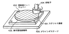
まず、蛍光体CsIの単結晶を作る。大口径の単結晶を作製するには、一般にブリッジマン炉を利用し、単結晶のインゴットとして作製する。インゴットの大きさとして、本実施例では直径300mm、厚さ100mmの単結晶を作った。更にこれから、適当なスライス装置で、厚さ1mmの単結晶CsIウエハーを切り出した。
【0033】
次に、図1に示すように、この単結晶CsIウエハー102を、厚さ5mmの第1の基板としてのステンレス基板101に貼り合わせる。
【0034】
この貼り合わせ方法としては、いろいろな方法があるが、その後の研磨時及び切断時の機械的な力に耐えられる強度があり、かつ、第2の基板との貼り合わせ後に、容易に剥すことが可能な貼り合わせ方法であれば良く、粘着剤による方法や、真空吸引力による方法や、熱可塑性接着剤による方法等が可能である。
【0035】
熱可塑性接着剤としては、酢酸ビニル系、アクリル系、スチレン系、セルロース系、ポリアミド系、アルキド系、モノマータイプのシアノアクリレート系がある。
【0036】
本実施例では、本実施例の特徴でもある熱可塑性接着剤103として、アクリル系接着剤を粉霧装置で着けて使用した。機械的強度がとれるのに充分な程度の接着でよい。
【0037】
このステンレス基板は、研磨装置のステージ105に装着できる構造になっている。この研磨工程では、単結晶CsIを後に述べるように500μmまで研磨するので、研磨後の単結晶CsIウエハーを支持するために、この基板を用い、これ以後は、この基板ごと次工程に使う。
【0038】
このステンレス基板は、±10μm以内の表面精度を持っており、このステンレス基板に貼り合わせをする場合の樹脂層(接着剤層)の厚さの精度も同程度に保つ必要がある。
【0039】
このステンレス基板ごと、専用のグラインダーに設置し、厚さ500μmまで単結晶CsIの表面を回転子104により研磨した。このスライスされた単結晶CsIウエハーを研磨することにより、放射線検出装置に最適な膜厚の蛍光体を作り上げることができる。更に画像読取装置との接着での精度をあげるために平坦化の研磨もかねる。
【0040】
次に、図2に示すように、この研磨した単結晶CsIウエハーを200mm角の大きさに切り出した。このカット工程は研磨工程の前後どちらに入れてもかまわない。本実施例では研磨工程の後に入れた。このときステンレス基板はカット装置のステージ107にも装着できるようになっている。
【0041】
本実施例では、単結晶CsIをスライスしたまま用いているが、ここで、単結晶CsIのセンサと反対面(X線側)、つまりステンレス基板側の単結晶CsI表面に光反射用の金属層を設けることで、発生した光を有効利用することもできる。この反射膜は、蒸着装置を使い、金属膜をあらかじめ蒸着しておいてもよい。あるいは、単結晶CsIを第2の基板との貼り合わせ、しかる後、第1の基板を単結晶CsIから剥離した後、この単結晶CsI上に、Al等の金属を含む反射シート等を更に貼り合わせても良い。
【0042】
次に、図3に示すように、光電変換素子、スイッチング素子としての薄膜トランジスタ、容量、配線を有する画像読取装置を作成した第2の基板としてのガラス基板108を用意する。これは2次元の画像読取装置となっている。
【0043】
ガラス基板の最上層はポリイミド保護層からなり、このガラス基板上の光電変換素子に、第1の基板側の単結晶CsI面を貼り合わせる。この貼り合わせは、研磨した蛍光体面を光電変換素子面に相対するように、樹脂系接着剤111で貼りあわせる。接着剤111としては、本実施例では光電変換素子の保護層と同じ材料であるポリイミド樹脂を用いた。ポリイミドは熱硬化性であり、図4に示すように、一度熱を加えて接着硬化させる。
【0044】
次に、この第1の基板をそのまま残しておくと、ここでX線を吸収してしまうので、この基板は取り去る必要がある。研磨時のステンレス基板と研磨した単結晶CsIウエハーを接着している熱可塑性接着剤は熱を加えることで接着力を失うので、熱硬化性のポリイミドが硬化した後、図4に示すように、再度熱を加えながら、図5に示すように、ステンレス基板を取り除くことができる。
【0045】
これにより、薄く研磨したCsIの単結晶膜のみを2次元の画像読取装置上に貼り合わせることができた。取り除いたステンレス基板は、洗浄後再利用される。
【0046】
図6を用いて、前述した画像読取装置の概略を説明する。図6は、2次元画像読取装置の1画素分の構造を示す図であり、(a)は平面図、(b)は、平面図(a)のA−B断面図を示す。
この画像読取装置は、図6に示すように、光電変換素子S11、及び薄膜トランジスタT11で構成されている。SIGは信号配線である。また、図6において、201はガラス基板、202は水素化非晶質窒化シリコン層のゲート絶縁膜、203はイントリンシック水素化非晶質シリコン層、204はN+ 型水素化非晶質シリコン層、205はドレイン電極、206は保護層、208はゲート電極、209はソース電極、210は熱硬化性ポリイミド樹脂系接着剤、211は研磨後の単結晶CsIウエハ(単結晶蛍光体)である。
【0047】
光により、光電変換素子S11で発生した電荷は、薄膜トランジスタT11を通して、蓄積容量に蓄えられたのち、不図示の読み出し回路で、この電荷を読み出す。図中MIS型光電変換素子上の212は、N+ 型水素化非晶質シリコン層であり、窓層として機能している。後述するように、このN+ 型水素化非晶質シリコン層は注入阻止層(ブロッキング層)、電極層としても機能している。
【0048】
図7は、この画像読取装置1画素の等価回路を示す。MIS型光電変換素子S11、信号転送用としての薄膜トランジスタT11で構成されている。さらにSignは信号配線である。gnは薄膜トランジスタのゲート線、D,GはそれぞれMIS型光電変換素子の上電極、下電極を示す。Cgs,Cgdは薄膜トランジスタのゲート電極とソース電極、ドレイン電極との重なりによる容量である。
【0049】
光により、光電変換素子S11で発生した電荷は、薄膜トランジスタT11を通して、Cgs,Cgdに蓄えられたのち、不図示の読み出し回路で、この電荷を読み出す。ここでは1ビットについての場合であるが、実際にはこのCgs,Cgdは、このゲート線につながった他の薄膜トランジスタのものとの合計である。
【0050】
なお、本実施例で用いられる光電変換素子は、特願平5−331690号公報において開示された光電変換素子と同じ原理によるものである。また薄膜トランジスタと光電変換素子はともに同一のプロセスにより作成され、ともにMIS型の構造を持っている。
【0051】
次に本実施例で用いた画像読取装置に用いられている光電変換素子の動作について簡単な説明をする。
【0052】
図8(a),(b)は、それぞれリフレッシュモード、光電変換モードの動作を示す光電変換素子のエネルギーバンド図である。図中の1〜5は各層の厚さ方向の状態を示している。
【0053】
リフレッシュモード(a)において、D電極はG電極に対して負の電位が与えられているために、イントリンシック水素化非晶質シリコン層3内の黒丸で示されたホールは電界によりD電極に導かれる。同時に白丸で示された電子はイントリンシック水素化非晶質シリコン層3に注入される。このとき一部のホールと電子はN+ 型水素化非晶質シリコン層2、イントリンシック水素化非晶質シリコン層3中において再結合して消滅する。充分に長い時間この状態が続けば、イントリンシック水素化非晶質シリコン層3内のホールはイントリンシック水素化非晶質シリコン層3から掃き出される。
【0054】
この状態で、光電変換モード(b)になると、D電極はG電極に対して正の電位が与えられるために、イントリンシック水素化非晶質シリコン層3中の電子は瞬時にD電極に導かれる。しかし、ホールはN+ 型水素化非晶質シリコン層2が注入阻止層として働くために、イントリンシック水素化非晶質シリコン層3中に導かれることはない。
【0055】
この状態で、イントリンシック水素化非晶質シリコン層3内に光が入射すると、光は吸収され、電子、ホール対が発生する。この電子は電界により電極に導かれ、ホールはイントリンシック水素化非晶質シリコン層3内を移動し水素化非晶質窒化シリコン層4の界面に達するが、ここで阻止されイントリンシック水素化非晶質シリコン層3内に留まることになる。このとき電子はD電極に移動し、ホールはイントリンシック水素化非晶質シリコン層3内の水素化非晶質窒化シリコン層4界面に移動するため、素子内の電気的中性を保つために、電流がG電極から流れる。この電流は光により発生した電子、ホール対に対応するので、入射した光に比例する。
【0056】
図9に、画像読取装置の全体回路図を示す。光電変換素子、駆動用薄膜トランジスタ、配線等は同一のプロセスにより、同一基板上に形成することができる。回路図中、S11〜S33は光電変換素子を表し、T11〜T33は光電変換素子駆動用薄膜トランジスタである。Vsは読み出し用電源、Vgはリフレッシュ用電源であり、それぞれスイッチSWs,SWgを介して全光電変換素子S11〜S33の下電極Gに接続されている。スイッチSWsはインバータを介して、スイッチSWgは、直接に、リフレッシュ制御回路RFに接続されており、リフレッシュ期間はスイッチSWgがON、その他の期間はスイッチSWsがONするように制御されている。信号出力は信号配線SIGにより検出用集積回路ICに接続されている。
【0057】
図9では、9個の画素を3個のブロックに分け、1ブロックあたり3画素の出力を同時に転送し、この信号は、検出用集積回路によって順次出力に変換され出力される。説明しやすいように9画素の2次元画像入力部としたが、実際にはさらに高密度の画素構成となっている。たとえば画素サイズを150μm角の大きさで、20cm角の画像読取装置を作成した場合、画素数はおよそ200万画素となる。
【0058】
[本実施例の効果]
本実施例によれば、蛍光体として単結晶CsIを用いているため、従来の蛍光板に比べ、充填効率が増え(100%)、また、光の透過率が高いため、光の散乱がない。そのため、X線の吸収効率、利用効率が上がり、さらにX線の吸収により発生した可視光の利用効率も向上するため、充分高感度な2次元放射線検出装置を提供することができた。
【0059】
[実施例2]
図10〜図14に本実施例の製造方法を示す。
【0060】
スライスした単結晶CsIウエハーまでの製法は、実施例1と共通なので省略する。この単結晶CsIウエハーを厚さ5mmの第1のステンレス基板に設置する。そのために以下の方法をとる。
【0061】
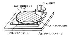
まず、図10に示すように、単結晶CsIウエハー602をウエハーシート603上に貼り合わせる。ウエハーシート603は、一般にシリコンウエハーをスライスする時に使う、粘着剤つきのシートである。これより同等の働きをするシートをウエハーシートと呼ぶことにする。本実施例でのウエハーシートは、両面がポリアミド系の熱可塑性粘着剤を塗布した形態のものを用いる。熱可塑性粘着剤に関しては、実施例1で述べたようなものが使用できる。引き続きウエハーシートに貼り合わせた単結晶CsIウエハーを厚さ5mmのステンレス基板601に貼り合わせる。
【0062】
この後、このステンレス基板ごとグラインダーに設置し、厚さ500μmまで単結晶CsI602の表面を研磨する。研磨後グラインダーから基板ごと取り出し、乾燥させる。
【0063】
次に、図11に示すように、この研磨した単結晶CsIウエハーを200mm角の大きさに切り出した。このカット工程は研磨工程の前後どちらに入れてもかまわない。本実施例では研磨工程の後に入れた。このときステンレス基板はカット装置のステージ607にも装着できるようになっている。
【0064】
次に、図12に示すように、光電変換素子、スイッチング素子としての薄膜トランジスタ、容量、配線を有する画像読取装置を作成した第2の基板としてのガラス基板608を用意する。
【0065】
ガラス基板の最上層はポリイミドの保護層からなる。本実施例で用いられる画像読取装置は実施例1で用いたものと同じものを用いた。
【0066】
研磨した蛍光体面を光電変換素子面に相対するように、接着剤611で貼りあわせる。接着剤611としては、本実施例では光電変換素子の保護層と同じ材料のポリイミド樹脂を用いた。ポリイミドは熱硬化性であり、図13に示すように、一度熱を加え接着硬化させる。
【0067】
次に、この第1の基板をそのまま残しておくと、ここでX線を吸収してしまうので、この基板は取り去る必要がある。研磨時のステンレス基板と研磨した単結晶CsIウエハーを接着しているウエハーシートの熱可塑性粘着剤は熱を加えることで接着力を失うので、熱硬化性接着剤であるポリイミドが硬化した後、再度熱を加えながら、図14に示すように、ステンレス基板を取り除くことができる。
【0068】
引き続き、ウエハーシート603を剥離する。
【0069】
これにより、薄く研磨したCsIの単結晶膜のみを2次元の画像読取装置上に貼り合わせることができた。取り除いたステンレス基板は、洗浄後再利用される。本実施例ではステンレス基板を剥した後、ウエハーシート603を剥したが、この順番は工程上、適宜変更してもかまわない。
【0070】
本実施例では単結晶CsIをスライスしたまま用いているが、ここで、単結晶CsIのセンサと反対面(X線側)、つまりウエハーシート側に光反射用の金属層を設けることで、発生した光を有効利用することもできる。この反射膜は、蒸着装置を使い、金属膜をあらかじめ蒸着してもよい。また単結晶CsIの貼り合わせた後にAl等の金属を含む反射シート等を更に貼り合わせても良い。
【0071】
[本実施例の効果]
本実施例によれば、蛍光体として単結晶CsIを用いているため、従来の蛍光板に比べ、充填効率が増え(100%)、また、光の透過率が高いため、光の散乱がない。そのため、X線の吸収効率、利用効率が上がり、さらにX線の吸収により発生した可視光の利用効率も向上し、充分高感度な2次元放射線検出装置を提供することができた。
【0072】
更にウエハーシートを利用しているので、作業性が向上した。
【0073】
[実施例3]
図15〜図20に本実施例の製造方法を示す。スライスした単結晶CsIウエハーまでの製法は実施例1と共通なので省略する。
【0074】
この単結晶CsIウエハーを厚さ5mmのステンレス基板に設置する。
【0075】
まず、図15に示すように、単結晶CsIウエハー702をウエハーシート703上に貼り合わせる。本実施例でのウエハーシート703は、片面にポリアミド系熱可塑性粘着剤が塗布されたものを使う。この粘着剤で単結晶CsIウエハーとウエハーシートを貼り合わせる。粘着剤としては熱可塑性のものであればかまわず、実施例1のようなものが使用できる。
【0076】
しかる後、ウエハーシート703に貼り合わせた単結晶CsIウエハー702を厚さ5mmのステンレス基板701に装着する。装着の方法としては、機械的に固定してもよいし、真空引きの機構を考えてもよい。研磨時に充分な強度でウエハーを保持できればよい。
【0077】
この基板ごとグラインダーステージ705に設置し、厚さ500μmまで単結晶CsIウエハーの表面を研磨した。研磨後グラインダーから基板ごと取り出し、乾燥させた。
【0078】
次に、図16に示すように、この研磨した単結晶CsIウエハーを200mm角の大きさに切り出した。このカット工程は研磨工程の前後どちらに入れてもかまわない。本実施例では研磨工程の後に入れた。このときステンレス基板はカット装置のステージにも装着できるようになっている。
【0079】
次に、図17に示すように、光電変換素子、スイッチング素子として薄膜トランジスタ、容量、配線を有する画像読取装置を作成した第2の基板としてガラス基板708を用意する。
【0080】
ガラス基板の最上層はポリイミドの保護層からなる。本実施例で用いた画像読取装置は実施例1で用いたものと同じものを用いた。
【0081】
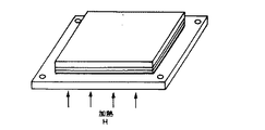
このガラス基板上の光電変換素子に単結晶CsIの研磨面が相対するように、樹脂系接着剤711で貼り合わせた。
【0082】
次に、この第1の基板をそのまま残しておくと、ここでX線を吸収してしまうので、この基板は取り去る必要がある。接着剤硬化後、単結晶CsIウエハーを支持していたステンレス基板を、図18のように加熱する。ウエハーシートの熱可塑性粘着剤は、熱を加えることで、その接着力を失うので、図19のようにステンレス基板のみを取り外すことができる。
【0083】
この時、図20に示すように、ウエハーシート703を単結晶CsIウエハー上に残すことになる。しかる後、このウエハーシート703を単結晶CsIウエハーの表面保護シートとして利用するため、ウエハーの外周部を封止剤712で封止する。
【0084】
本実施例では、単結晶CsIをスライスしたまま用いているが、ここで、単結晶CsIのセンサと反対面、つまりウエハーシート側に光反射用の金属層を設けることで、発生した光を有効に利用することもできる。この反射膜は蒸着装置を使い、直接単結晶CsI上に金属膜をつけてもよいし、また、単結晶CsIを貼り合わせた後に、ウエハーシート上にアルミシートなどの反射層を更に加えるなどしても良い。
【0085】
[本実施例での効果]
本実施例によれば、蛍光体として単結晶CsIを用いているため、従来の蛍光板に比べ、充填効率が増え(100%)、また、光の透過率が高いため、光の散乱がない。そのためX線の吸収効率が上がり、さらにX線の吸収により発生した可視光の利用効率も向上し、充分高感度な2次元放射線検出装置を作製することができた。
【0086】
更に、ウエハーシートを利用しているので、作業性が向上した。
【0087】
また更に、ウエハーシートをそのまま、蛍光体の保護層として使えるので、簡略な工程で、貼り合わせと保護膜作製を行うことができた。
【0088】
[実施例4]
以下、本発明の実施例4について説明する。
【0089】
スライスした単結晶CsIウエハーまでの製法は実施例1と共通なので省略する。
【0090】
この単結晶CsIウエハーを厚さ200μmのステンレス基板に設置する。
【0091】
まず単結晶CsIウエハーをウエハーシート上に貼り合わせる。本実施例でのウエハーシートは、片面に熱可塑性粘着剤が塗布されたものを使う。この粘着剤で単結晶CsIウエハーとウエハーシートを貼り合わせる。粘着剤としては熱可塑性のものであればかまわず、実施例1のようなものが使用できる。さらにこのウエハーシートには金属膜が作り込まれている。どちらの面に作り込んでもよい。あるいはラミネート構造で金属膜を挟み込んでもよい。
【0092】
しかる後、ウエハーシートに貼り合わせた単結晶CsIウエハーを厚さ5mmのステンレス基板に装着する。この基板ごとグラインダーに設置し、厚さ500μmまで単結晶CsIの表面を研磨した。研磨後グラインダーから基板ごと取り出し、乾燥させた。
【0093】
次に、この研磨した単結晶CsIウエハーを200mm角の大きさに切り出した。このカット工程は研磨工程の前後どちらに入れてもかまわない。本実施例では研磨工程の後に入れた。このときステンレス基板はカット装置のステージにも装着できるようになっている。
【0094】
次に光電変換素子、スイッチング素子としての薄膜トランジスタ、容量、配線を有する画像読取装置を作成したガラス基板を用意する。画像読取装置の部分は実施例1と同じものを用いた。
【0095】
このガラス基板上の光電変換素子に単結晶CsI研磨面が相対するように、樹脂系接着剤で貼り合わせる。
【0096】
次に、この第1の基板をそのまま残しておくと、ここでX線を吸収してしまうので、この基板は取り去る必要がある。接着剤硬化後、単結晶CsIウエハーを支持していたステンレス基板を取り外す。
【0097】
この時、ウエハーシートを単結晶CsIウエハー上に残すことになる。しかる後、このウエハーシートを単結晶CsIウエハーの表面保護シートとして利用するため、ウエハーの外周部を封止剤で封止する。
【0098】
以上の工程により、図21に示すように、反射膜(金属膜804)付き保護シート(ウエハーシート805)を、単結晶CsIの上に付けた形で放射線検出装置を作製することができた。
【0099】
[本実施例での効果]
本実施例によれば、蛍光体として単結晶CsIを用いているため、従来の蛍光板に比べ、充填効率が増え(100%)、また、光の透過率が高いため、光の散乱がない。そのため、X線の吸収効率が上がり、さらにX線の吸収により発生した可視光の利用効率も向上し、充分高感度な2次元放射線検出装置を作製することができた。
【0100】
更に、ウエハーシートを利用しているので、作業性が向上した。
【0101】
更に、ウエハーシートをそのまま、蛍光体の保護層として使えるので、簡略な工程で、貼り合わせと保護膜作製を行うことができた。
【0102】
更にまた、このウエハーシートには金属膜が作り込まれているので、蛍光体中で発生した光の反射板としても効果を発揮する。つまり光電変換素子と反対方向へ進む光は、この金属膜で反射され、光電変換素子の方向へ入射することになり、利用効率が向上した。
【0103】
また、金属膜を設けたため、耐湿性も向上した。
【0104】
【発明の効果】
以上説明したように、本発明によれば、最適化された厚さを持つ蛍光体として、大面積単結晶CsIを用いるので、100%充填率となり、X線の利用効率が向上し、放射線検出装置の高感度化ができる。
【0105】
また単結晶なので、光の散乱吸収による損失が低く抑えられ、また非常に高い透過率を有するため、X線吸収により発生した可視光の利用効率が向上する。
【0106】
また、本発明によれば、作製工程中に、研磨工程を導入したため、単結晶CsIの厚さを自由に設定できるようになり、感度、明細度を最適にする設計が容易になり、その結果、充分な明細度で高感度な放射線検出装置を作製することができるようになった。
【0107】
更に、ウエハーシートを利用することにより、作業性が向上する。
【0108】
更に、ウエハーシートをそのまま、蛍光体の保護層として使えるので、簡略な工程で、貼り合わせと保護膜作製を行うことができる。
【0109】
更にまた、金属膜を有するウエハーシートを用いることにより、蛍光体中で発生した光の反射板としても効果を発揮する。つまり光電変換素子と反対方向へ進む光は、この金属膜で反射され、光電変換素子の方向へ入射することになり、利用効率が向上する。
【0110】
また、金属膜を設けたため、耐湿性も向上する。
【0111】
このように、本発明は、高品質、高感度な大面積放射線検出装置を、簡易なプロセスで容易に提供することができた。
【図面の簡単な説明】
【図1】本発明になる実施例1の放射線検出装置の製造工程を示す斜視図である。
【図2】本発明になる実施例1の放射線検出装置の製造工程を示す斜視図である。
【図3】本発明になる実施例1の放射線検出装置の製造工程を示す斜視図である。
【図4】本発明になる実施例1の放射線検出装置の製造工程を示す斜視図である。
【図5】本発明になる実施例1の放射線検出装置の製造工程を示す斜視図である。
【図6】本発明になる実施例1の放射線検出装置の1画素の平面図(a)、及びそのA−B断面図(b)である。
【図7】1画素分の等価回路図である。
【図8】光電変換素子の動作原理を示すエネルギーバンド図である。
【図9】画像入力部の全体回路図である。
【図10】本発明になる実施例2の放射線検出装置の製造工程を示す斜視図である。
【図11】本発明になる実施例2の放射線検出装置の製造工程を示す斜視図である。
【図12】本発明になる実施例2の放射線検出装置の製造工程を示す斜視図である。
【図13】本発明になる実施例2の放射線検出装置の製造工程を示す斜視図である。
【図14】本発明になる実施例2の放射線検出装置の製造工程を示す斜視図である。
【図15】本発明になる実施例3の放射線検出装置の製造工程を示す斜視図である。
【図16】本発明になる実施例3の放射線検出装置の製造工程を示す斜視図である。
【図17】本発明になる実施例3の放射線検出装置の製造工程を示す斜視図である。
【図18】本発明になる実施例3の放射線検出装置の製造工程を示す斜視図である。
【図19】本発明になる実施例3の放射線検出装置の製造工程を示す斜視図である。
【図20】本発明になる実施例3の放射線検出装置の製造工程を示す斜視図である。
【図21】本発明になる実施例4の放射線検出装置の製造方法を示す斜視図である。
【図22】従来の放射線検出装置の平面図(a)、及び断面図(b)である。
【符号の説明】
108,201,608,708,801,901 ガラス基板
101,601,701 ステンレス基板
102,602,702 単結晶CsIウエハ
110,211,610,710,803 研磨後の単結晶CsIウエハ
103 熱可塑性樹脂(熱可塑性接着剤)
603,703,805 ウエハシート
105,605,705 グラインダステージ
106,606,706 カッティングブレード
107,607,707 カッティング装置ステージ
111,611,711,910 接着剤
H 加熱
109,609,709,802 光電変換素子等の層
712 封止剤
804 金属層
208,908 ゲート電極
202,902 水素化非晶質窒化シリコン層のゲート絶縁膜
203,903 イントリンシック水素化非晶質シリコン層
204,904 N+ 型水素化非晶質シリコン層
209,909 ソース電極
205,905 ドレイン電極
206,906 保護層
911 蛍光体粒子
912 バインダー
913 基台[0001]
BACKGROUND OF THE INVENTION
The present invention relates to a method for manufacturing a radiation detection apparatus, and more particularly to a method for manufacturing a radiation detection apparatus that can easily manufacture a radiation detection apparatus having a high sensitivity and a large area.
[0002]
[Prior art]
In general, in order to detect radiation, particularly X-rays, a radiation detection device comprising a combination of a phosphor for converting X-rays into visible light and an image reading device for detecting light emitted from the phosphor is used. It is done. Such a radiation detection apparatus is also used in medicine. For example, when producing an X-ray detection apparatus for chest radiography, a two-dimensional image reading apparatus is provided with a fluorescent plate (made of a fluorescent powder, a plate-like fluorescent substance). The structure which bonds together is known. X-ray chest imaging requires a large area, and fluorescent screens are easy to use because they can be easily obtained with a uniform thickness and large area.
[0003]
Hereinafter, a conventional example of manufacturing a two-dimensional radiation detection apparatus by attaching a fluorescent plate on a two-dimensional image reading apparatus will be described.
[0004]
As a two-dimensional image reading apparatus, a photoelectric conversion element using amorphous silicon, a thin film transistor and the like arranged two-dimensionally are used as a large-area image reading apparatus.
[0005]
22A and 22B are diagrams showing the structure of one pixel of a conventional two-dimensional image reading apparatus, in which FIG. 22A is a plan view and FIG. 22B is a cross-sectional view taken along the line AB of FIG.
[0006]
In FIG. 22, S11 is a photoelectric conversion element portion, and T11 is a photoelectric conversion element driving thin film transistor portion. 901 is a glass substrate, 902 is a gate insulating film of a hydrogenated amorphous silicon nitride layer, 903 is an intrinsic hydrogenated amorphous silicon layer, and 904 is N+ Type hydrogenated amorphous silicon layer, 905 is a drain electrode, 906 is a protective layer, 908 is a gate electrode, 909 is a source electrode, 910 is an adhesive, 911 is a phosphor particle, 912 is a binder, and 913 is a base. .
[0007]
Conventionally, a two-dimensional radiation detection apparatus has been manufactured by attaching a fluorescent plate with an adhesive on an image reading apparatus in which a large number of pixels are arranged in this way.
[0008]
[Problems to be solved by the invention]
However, in the above-described conventional example, as shown in FIG. 22, the fluorescent plate is prepared by kneading phosphor powder 911 with a resin binder 912 and applying it onto a base 913. Therefore, there is a drawback that the filling rate of the phosphor 911 is low, and the utilization efficiency of X-rays is reduced accordingly.
[0009]
If an attempt is made to increase the filling rate in order to increase the X-ray utilization efficiency, the entire phosphor screen becomes fragile and difficult to handle.
[0010]
If you try to increase the sensitivity by increasing the thickness, the light generated by absorbing X-rays will be scattered and absorbed by the binder, powder, or their interface, and if it is too thick, the light transmission efficiency will decrease. It was.
[0011]
As described above, in the conventional method using a fluorescent plate, the utilization efficiency of X-rays is low and the amount of output light is small, so the sensitivity is low.
[0012]
For example, when a two-dimensional radiation detection apparatus is used in medicine, the X-ray dose cannot be significantly increased, so that the sensitivity is low.
[0013]
As a result of the low sensitivity of the fluorescent plate, there has been a problem that a very high sensitivity is required for the photoelectric conversion element itself utilizing the light emitted therefrom.
[0014]
[Object of invention]
The object of the present invention is to provide a high sensitivity in which light is not scattered and absorbed by the binder and powder in the fluorescent plate or their interface as in the prior art, and the light transmission efficiency does not decrease even when the thickness is increased. An object of the present invention is to obtain a radiation detection apparatus provided with a simple phosphor.
[0015]
In addition, the phosphor filling ratio is increased without increasing the brittleness, so that the use efficiency of radiation is high, the handling is easy, and even if the thickness is increased to increase the sensitivity, the light transmission efficiency does not decrease, and the sensitivity is high. It is providing the radiation detection apparatus provided with.
[0016]
[Means for solving problems]
As a means for solving the above problems, the present invention provides:
Single crystal phosphorAnd a wafer sheet having a metal film for reflecting light generated by the single crystal phosphor is applied to the wafer sheet.Thermoplastic adhesiveA first bonding step of mounting a first substrate on a surface opposite to the surface of the wafer sheet on which the single crystal phosphor is bonded;
Polishing and planarizing the single crystal phosphor after the first bonding step, cutting the single crystal phosphor after planarization, and
A thermosetting adhesive is used on the flat surface of the single crystal phosphor on the first substrate on the second substrate on which the image reading device for converting light emitted from the single crystal phosphor into electricity is formed. A second bonding step of bonding by material;
A step of removing the first substrate after the second bonding step;
Sealing the periphery of the single crystal phosphor with a sealant after the step of removing the first substrate;
The manufacturing method of the radiation detection apparatus characterized by having is provided.
[0022]
In addition, the image reading device includes a first electrode layer, a first conductivity type carrier, and a first insulation layer that blocks passage of a second conductivity type carrier different from the first conductivity type on the insulating substrate. Photoelectric conversion in which a semiconductor layer, a second electrode layer, and an injection element layer between the second electrode layer and the photoelectric conversion layer and blocking injection of a first conductivity type carrier into the photoelectric conversion layer are stacked. A plurality of photoelectric conversion elements are arranged two-dimensionally, the switch elements are connected to the photoelectric conversion elements, and the photoelectric conversion elements are divided into a plurality of blocks. Also, the present invention is a method for manufacturing a radiation detection apparatus, which is an image reading apparatus that detects an optical signal by operating the switch element for each block.
[0023]
The switch element applies an electric field to the photoelectric conversion element in a direction to guide the first conductivity type carrier from the photoelectric conversion semiconductor layer to the second electrode layer in the refresh operation, and in the photoelectric conversion operation, the switch element The first conductivity type carriers generated by light incident on the photoelectric conversion semiconductor layer remain in the photoelectric conversion semiconductor layer, and the second conductivity type carriers are guided in the direction leading to the second electrode layer. An electric field is applied to the conversion element, and the first carrier accumulated in the photoelectric conversion semiconductor layer by the photoelectric conversion operation or the second conductivity type carrier introduced to the second electrode layer is detected as an optical signal. It is also the manufacturing method of the radiation detection apparatus characterized by being controlled by.
[0024]
[Action]
According to the present invention, by using a single crystal phosphor such as a large area single crystal CsI as a phosphor having an optimized thickness, the filling rate becomes 100%, the X-ray utilization efficiency is improved, and the radiation The sensitivity of the detection device can be increased.
[0025]
Further, since it is a single crystal, loss due to light scattering and absorption is kept low, and it has a very high transmittance, so that the utilization efficiency of visible light generated by X-ray absorption is improved.
[0026]
In addition, according to the present invention, since the polishing process of the single crystal phosphor is introduced during the manufacturing process, the thickness of the phosphor such as single crystal CsI can be freely set, and the sensitivity and the detail are optimized. As a result, it has become possible to produce a highly sensitive radiation detection apparatus with sufficient detail.
[0027]
Further, since a wafer sheet is used, workability is improved.
[0028]
Furthermore, since the wafer sheet can be used as it is as a protective layer of the phosphor, it can be bonded and a protective film can be produced in a simple process.
[0029]
Furthermore, since a metal film is formed on the wafer sheet, the wafer sheet is also effective as a reflector for the light generated in the phosphor. That is, the light traveling in the direction opposite to the photoelectric conversion element is reflected by the metal film and is incident in the direction of the photoelectric conversion element, so that utilization efficiency is improved.
[0030]
Further, since the metal film is provided, the moisture resistance is also improved.
[0031]
DETAILED DESCRIPTION OF THE INVENTION
[Example 1]
1 to 5 show a manufacturing process of the radiation detection apparatus according to the present embodiment.
[0032]
First, a single crystal of phosphor CsI is made. In order to produce a large-diameter single crystal, a Bridgman furnace is generally used to produce a single crystal ingot. In this example, a single crystal having a diameter of 300 mm and a thickness of 100 mm was made as the size of the ingot. Further, from this, a single crystal CsI wafer having a thickness of 1 mm was cut out with an appropriate slicing apparatus.
[0033]
Next, as shown in FIG. 1, the single crystal CsI wafer 102 is bonded to a stainless steel substrate 101 as a first substrate having a thickness of 5 mm.
[0034]
There are various methods for bonding, but there is a strength that can withstand the mechanical force at the time of subsequent polishing and cutting, and it can be easily peeled off after bonding to the second substrate. Any bonding method can be used, and a method using an adhesive, a method using a vacuum suction force, a method using a thermoplastic adhesive, and the like are possible.
[0035]
Examples of the thermoplastic adhesive include vinyl acetate, acrylic, styrene, cellulose, polyamide, alkyd, and monomer type cyanoacrylate.
[0036]
In the present example, an acrylic adhesive was used as a thermoplastic adhesive 103, which is also a feature of the present example, with a dust mist device. Adhesion to a degree sufficient to obtain mechanical strength is sufficient.
[0037]
This stainless steel substrate has a structure that can be mounted on the stage 105 of the polishing apparatus. In this polishing step, the single crystal CsI is polished to 500 μm as will be described later, so that this substrate is used to support the single crystal CsI wafer after polishing, and thereafter, this substrate is used in the next step.
[0038]
This stainless steel substrate has a surface accuracy within ± 10 μm, and the accuracy of the thickness of the resin layer (adhesive layer) when bonded to this stainless steel substrate needs to be kept at the same level.
[0039]
Each stainless steel substrate was placed in a dedicated grinder, and the surface of the single crystal CsI was polished by the rotor 104 to a thickness of 500 μm. By polishing the sliced single crystal CsI wafer, a phosphor having a film thickness optimum for the radiation detection apparatus can be formed. Further, in order to increase the accuracy in bonding with the image reading apparatus, polishing for flattening can also be performed.
[0040]
Next, as shown in FIG. 2, the polished single crystal CsI wafer was cut into a size of 200 mm square. This cutting process may be performed before or after the polishing process. In this example, it was added after the polishing step. At this time, the stainless steel substrate can be mounted on the stage 107 of the cutting apparatus.
[0041]
In the present embodiment, the single crystal CsI is used while being sliced. Here, a light reflecting metal layer is formed on the surface of the single crystal CsI opposite to the sensor of the single crystal CsI (X-ray side), that is, on the surface of the single crystal CsI on the stainless steel substrate side. By providing the light, the generated light can be used effectively. The reflective film may be vapor-deposited in advance using a vapor deposition apparatus. Alternatively, the single crystal CsI is bonded to the second substrate, and then the first substrate is peeled from the single crystal CsI, and then a reflective sheet containing a metal such as Al is further bonded to the single crystal CsI. May be combined.
[0042]
Next, as shown in FIG. 3, a glass substrate 108 as a second substrate on which an image reading device having a photoelectric conversion element, a thin film transistor as a switching element, a capacitor, and a wiring is prepared. This is a two-dimensional image reading apparatus.
[0043]
The uppermost layer of the glass substrate is composed of a polyimide protective layer, and the single crystal CsI surface on the first substrate side is bonded to the photoelectric conversion element on the glass substrate. This bonding is performed with the resin adhesive 111 so that the polished phosphor surface faces the photoelectric conversion element surface. As the adhesive 111, polyimide resin, which is the same material as the protective layer of the photoelectric conversion element, was used in this example. Polyimide is thermosetting. As shown in FIG. 4, heat is applied once to cure the adhesive.
[0044]
Next, if this first substrate is left as it is, X-rays will be absorbed here, so this substrate needs to be removed. The thermoplastic adhesive that bonds the polished stainless steel substrate and the polished single crystal CsI wafer loses adhesive strength by applying heat, so after the thermosetting polyimide is cured, as shown in FIG. While applying heat again, the stainless steel substrate can be removed as shown in FIG.
[0045]
As a result, only the thinly polished CsI single crystal film could be bonded onto the two-dimensional image reading apparatus. The removed stainless steel substrate is reused after cleaning.
[0046]
The outline of the above-described image reading apparatus will be described with reference to FIG. 6A and 6B are diagrams showing the structure of one pixel of the two-dimensional image reading apparatus, in which FIG. 6A is a plan view and FIG.
As shown in FIG. 6, the image reading apparatus includes a photoelectric conversion element S11 and a thin film transistor T11. SIG is a signal wiring. In FIG. 6, 201 is a glass substrate, 202 is a gate insulating film of a hydrogenated amorphous silicon nitride layer, 203 is an intrinsic hydrogenated amorphous silicon layer, and 204 is N+ Type hydrogenated amorphous silicon layer, 205 is a drain electrode, 206 is a protective layer, 208 is a gate electrode, 209 is a source electrode, 210 is a thermosetting polyimide resin adhesive, 211 is a single crystal CsI wafer after polishing ( Single crystal phosphor).
[0047]
The charge generated by the photoelectric conversion element S11 due to light is stored in the storage capacitor through the thin film transistor T11, and then read out by a read circuit (not shown). In the figure, 212 on the MIS type photoelectric conversion element is N+Type hydrogenated amorphous silicon layer, which functions as a window layer. As will be described later, this N+The type hydrogenated amorphous silicon layer also functions as an injection blocking layer (blocking layer) and an electrode layer.
[0048]
FIG. 7 shows an equivalent circuit of one pixel of the image reading apparatus. It is composed of a MIS type photoelectric conversion element S11 and a thin film transistor T11 for signal transfer. Further, Sign is a signal wiring. gn represents a gate line of the thin film transistor, and D and G represent an upper electrode and a lower electrode of the MIS photoelectric conversion element, respectively. Cgs and Cgd are capacitances due to overlapping of the gate electrode, the source electrode, and the drain electrode of the thin film transistor.
[0049]
Charges generated by the photoelectric conversion element S11 due to light are stored in Cgs and Cgd through the thin film transistor T11, and then read out by a read circuit (not shown). Here, although it is a case of 1 bit, in reality, Cgs and Cgd are the sum of those of other thin film transistors connected to the gate line.
[0050]
The photoelectric conversion element used in this example is based on the same principle as the photoelectric conversion element disclosed in Japanese Patent Application No. 5-331690. The thin film transistor and the photoelectric conversion element are both manufactured by the same process, and both have a MIS type structure.
[0051]
Next, the operation of the photoelectric conversion element used in the image reading apparatus used in this embodiment will be briefly described.
[0052]
FIGS. 8A and 8B are energy band diagrams of the photoelectric conversion element showing operations in the refresh mode and the photoelectric conversion mode, respectively. 1-5 in the figure have shown the state of the thickness direction of each layer.
[0053]
In the refresh mode (a), since a negative potential is applied to the D electrode with respect to the G electrode, the holes indicated by the black circles in the intrinsic hydrogenated
[0054]
In this state, when the photoelectric conversion mode (b) is entered, since the D electrode is given a positive potential with respect to the G electrode, the electrons in the intrinsic hydrogenated
[0055]
When light enters the intrinsic hydrogenated
[0056]
FIG. 9 shows an overall circuit diagram of the image reading apparatus. The photoelectric conversion element, the driving thin film transistor, the wiring, and the like can be formed over the same substrate by the same process. In the circuit diagram, S11 to S33 represent photoelectric conversion elements, and T11 to T33 are thin film transistors for driving photoelectric conversion elements. Vs is a power source for reading and Vg is a power source for refreshing, which are connected to the lower electrodes G of all the photoelectric conversion elements S11 to S33 via switches SWs and SWg, respectively. The switch SWs is directly connected to the refresh control circuit RF via an inverter, and is controlled so that the switch SWg is ON during the refresh period and the switch SWs is ON during the other periods. The signal output is connected to the detection integrated circuit IC by a signal wiring SIG.
[0057]
In FIG. 9, 9 pixels are divided into 3 blocks, and the output of 3 pixels per block is simultaneously transferred. This signal is sequentially converted into an output by the integrated circuit for detection and output. For ease of explanation, a 9-pixel two-dimensional image input unit is used, but actually, the pixel configuration has a higher density. For example, when an image reading apparatus having a pixel size of 150 μm square and a 20 cm square is created, the number of pixels is approximately 2 million pixels.
[0058]
[Effect of this embodiment]
According to the present embodiment, since single crystal CsI is used as the phosphor, the filling efficiency is increased (100%) as compared with the conventional phosphor plate, and the light transmittance is high, so there is no light scattering. As a result, the X-ray absorption efficiency and utilization efficiency are improved, and the utilization efficiency of visible light generated by the X-ray absorption is also improved, so that a sufficiently sensitive two-dimensional radiation detection apparatus can be provided.
[0059]
[Example 2]
10 to 14 show the manufacturing method of this embodiment.
[0060]
Since the manufacturing method up to the sliced single crystal CsI wafer is the same as that in Example 1, the description thereof is omitted. This single crystal CsI wafer is placed on a first stainless steel substrate having a thickness of 5 mm. Therefore, the following method is taken.
[0061]
First, as shown in FIG. 10, a single crystal CsI wafer 602 is bonded onto a wafer sheet 603. The wafer sheet 603 is a sheet with an adhesive generally used when slicing a silicon wafer. A sheet that functions equivalently will be referred to as a wafer sheet. The wafer sheet used in this example is in a form in which both sides are coated with a polyamide-based thermoplastic adhesive. As the thermoplastic adhesive, those described in Example 1 can be used. Subsequently, the single crystal CsI wafer bonded to the wafer sheet is bonded to the stainless steel substrate 601 having a thickness of 5 mm.
[0062]
Thereafter, the stainless steel substrate is placed on a grinder, and the surface of the single crystal CsI 602 is polished to a thickness of 500 μm. After polishing, the whole substrate is taken out from the grinder and dried.
[0063]
Next, as shown in FIG. 11, this polished single crystal CsI wafer was cut into a size of 200 mm square. This cutting process may be performed before or after the polishing process. In this example, it was added after the polishing step. At this time, the stainless steel substrate can be mounted on the stage 607 of the cutting apparatus.
[0064]
Next, as shown in FIG. 12, a glass substrate 608 is prepared as a second substrate on which an image reading device having a photoelectric conversion element, a thin film transistor as a switching element, a capacitor, and wiring is formed.
[0065]
The uppermost layer of the glass substrate is made of a polyimide protective layer. The image reading apparatus used in the present embodiment is the same as that used in the first embodiment.
[0066]
The polished phosphor surface is bonded with an adhesive 611 so as to face the photoelectric conversion element surface. As the adhesive 611, polyimide resin of the same material as the protective layer of the photoelectric conversion element was used in this example. Polyimide is thermosetting. As shown in FIG. 13, heat is applied once to bond and cure.
[0067]
Next, if this first substrate is left as it is, X-rays will be absorbed here, so this substrate needs to be removed. The thermoplastic adhesive of the wafer sheet that bonds the polished stainless steel substrate and the polished single crystal CsI wafer loses its adhesive strength by applying heat, so after the polyimide, which is a thermosetting adhesive, is cured, While applying heat, the stainless steel substrate can be removed as shown in FIG.
[0068]
Subsequently, the wafer sheet 603 is peeled off.
[0069]
As a result, only the thinly polished CsI single crystal film could be bonded onto the two-dimensional image reading apparatus. The removed stainless steel substrate is reused after cleaning. In this embodiment, the wafer sheet 603 is peeled after the stainless steel substrate is peeled off, but this order may be appropriately changed in the process.
[0070]
In the present embodiment, the single crystal CsI is used while being sliced, but here, it is generated by providing a light reflecting metal layer on the surface opposite to the sensor of the single crystal CsI (X-ray side), that is, on the wafer sheet side. The used light can also be used effectively. This reflective film may be vapor-deposited in advance using a vapor deposition device. Further, a reflective sheet containing a metal such as Al may be further bonded after the single crystal CsI is bonded.
[0071]
[Effect of this embodiment]
According to the present embodiment, since single crystal CsI is used as the phosphor, the filling efficiency is increased (100%) as compared with the conventional phosphor plate, and the light transmittance is high, so there is no light scattering. Therefore, the X-ray absorption efficiency and utilization efficiency are increased, and the utilization efficiency of visible light generated by the X-ray absorption is improved, and a sufficiently sensitive two-dimensional radiation detection apparatus can be provided.
[0072]
In addition, since a wafer sheet is used, workability is improved.
[0073]
[Example 3]
15 to 20 show the manufacturing method of this embodiment. Since the manufacturing method up to the sliced single crystal CsI wafer is the same as that in Example 1, it is omitted.
[0074]
This single crystal CsI wafer is placed on a stainless steel substrate having a thickness of 5 mm.
[0075]
First, as shown in FIG. 15, a single crystal CsI wafer 702 is bonded onto a wafer sheet 703. As the wafer sheet 703 in this embodiment, one having a polyamide-based thermoplastic adhesive applied on one side is used. A single crystal CsI wafer and a wafer sheet are bonded together with this adhesive. The pressure-sensitive adhesive may be any thermoplastic one, and the one as in Example 1 can be used.
[0076]
Thereafter, the single crystal CsI wafer 702 bonded to the wafer sheet 703 is mounted on a stainless steel substrate 701 having a thickness of 5 mm. As a mounting method, it may be mechanically fixed or a vacuuming mechanism may be considered. It is sufficient that the wafer can be held with sufficient strength during polishing.
[0077]
The entire substrate was placed on a grinder stage 705, and the surface of the single crystal CsI wafer was polished to a thickness of 500 μm. After polishing, the substrate was taken out from the grinder and dried.
[0078]
Next, as shown in FIG. 16, this polished single crystal CsI wafer was cut into a size of 200 mm square. This cutting process may be performed before or after the polishing process. In this example, it was added after the polishing step. At this time, the stainless steel substrate can be mounted on the stage of the cutting apparatus.
[0079]
Next, as shown in FIG. 17, a glass substrate 708 is prepared as a second substrate on which an image reading device having a thin film transistor, a capacitor, and wiring as photoelectric conversion elements and switching elements is formed.
[0080]
The uppermost layer of the glass substrate is made of a polyimide protective layer. The image reading apparatus used in this example was the same as that used in Example 1.
[0081]
The photoelectric conversion element on the glass substrate was bonded with a resin adhesive 711 so that the polished surface of the single crystal CsI was opposed to the photoelectric conversion element.
[0082]
Next, if this first substrate is left as it is, X-rays will be absorbed here, so this substrate needs to be removed. After the adhesive is cured, the stainless steel substrate supporting the single crystal CsI wafer is heated as shown in FIG. Since the thermoplastic adhesive of the wafer sheet loses its adhesive force when heated, only the stainless steel substrate can be removed as shown in FIG.
[0083]
At this time, as shown in FIG. 20, the wafer sheet 703 is left on the single crystal CsI wafer. Thereafter, in order to use this wafer sheet 703 as a surface protective sheet for a single crystal CsI wafer, the outer periphery of the wafer is sealed with a sealant 712.
[0084]
In this embodiment, the single crystal CsI is used while being sliced. Here, the generated light is effectively provided by providing a metal layer for light reflection on the surface opposite to the sensor of the single crystal CsI, that is, on the wafer sheet side. It can also be used. The reflective film may be deposited directly on the single crystal CsI using a vapor deposition device, or after the single crystal CsI is bonded, a reflective layer such as an aluminum sheet is further added on the wafer sheet. May be.
[0085]
[Effect in this embodiment]
According to the present embodiment, since single crystal CsI is used as the phosphor, the filling efficiency is increased (100%) as compared with the conventional phosphor plate, and the light transmittance is high, so there is no light scattering. For this reason, the X-ray absorption efficiency has been improved, and the utilization efficiency of visible light generated by the X-ray absorption has been improved, and a sufficiently sensitive two-dimensional radiation detection apparatus has been produced.
[0086]
Furthermore, since a wafer sheet is used, workability is improved.
[0087]
Furthermore, since the wafer sheet can be used as it is as a protective layer of the phosphor, it is possible to perform bonding and protective film production by a simple process.
[0088]
[Example 4]
[0089]
Since the manufacturing method up to the sliced single crystal CsI wafer is the same as that in Example 1, it is omitted.
[0090]
This single crystal CsI wafer is placed on a 200 μm thick stainless steel substrate.
[0091]
First, a single crystal CsI wafer is bonded onto a wafer sheet. As the wafer sheet in this embodiment, one having a thermoplastic adhesive applied on one side is used. A single crystal CsI wafer and a wafer sheet are bonded together with this adhesive. The pressure-sensitive adhesive may be any thermoplastic one, and the one as in Example 1 can be used. Further, a metal film is formed on the wafer sheet. Either side can be built in. Alternatively, a metal film may be sandwiched with a laminate structure.
[0092]
Thereafter, the single crystal CsI wafer bonded to the wafer sheet is mounted on a stainless steel substrate having a thickness of 5 mm. The entire substrate was placed on a grinder and the surface of single crystal CsI was polished to a thickness of 500 μm. After polishing, the substrate was taken out from the grinder and dried.
[0093]
Next, the polished single crystal CsI wafer was cut into a size of 200 mm square. This cutting process may be performed before or after the polishing process. In this example, it was added after the polishing step. At this time, the stainless steel substrate can be mounted on the stage of the cutting apparatus.
[0094]
Next, a glass substrate on which an image reading device having a photoelectric conversion element, a thin film transistor as a switching element, a capacitor, and wiring is prepared is prepared. The same image reading apparatus as that in Example 1 was used.
[0095]
The single crystal CsI polished surface is bonded to the photoelectric conversion element on the glass substrate with a resin adhesive.
[0096]
Next, if this first substrate is left as it is, X-rays will be absorbed here, so this substrate needs to be removed. After the adhesive is cured, the stainless steel substrate supporting the single crystal CsI wafer is removed.
[0097]
At this time, the wafer sheet is left on the single crystal CsI wafer. Thereafter, in order to use this wafer sheet as a surface protective sheet for a single crystal CsI wafer, the outer periphery of the wafer is sealed with a sealant.
[0098]
Through the above steps, as shown in FIG. 21, the radiation detection apparatus was able to be manufactured in a form in which a protective sheet (wafer sheet 805) with a reflective film (metal film 804) was attached on the single crystal CsI.
[0099]
[Effect in this embodiment]
According to the present embodiment, since single crystal CsI is used as the phosphor, the filling efficiency is increased (100%) as compared with the conventional phosphor plate, and the light transmittance is high, so there is no light scattering. As a result, the absorption efficiency of X-rays is increased, the utilization efficiency of visible light generated by the absorption of X-rays is improved, and a sufficiently sensitive two-dimensional radiation detection apparatus can be produced.
[0100]
Furthermore, since a wafer sheet is used, workability is improved.
[0101]
Furthermore, since the wafer sheet can be used as it is as a protective layer of the phosphor, it is possible to perform bonding and protective film production in a simple process.
[0102]
Furthermore, since a metal film is formed on the wafer sheet, the wafer sheet is also effective as a reflector for the light generated in the phosphor. That is, the light traveling in the direction opposite to the photoelectric conversion element is reflected by the metal film and is incident in the direction of the photoelectric conversion element, thereby improving the utilization efficiency.
[0103]
Moreover, since the metal film was provided, the moisture resistance was also improved.
[0104]
【The invention's effect】
As described above, according to the present invention, since the large-area single crystal CsI is used as the phosphor having the optimized thickness, the filling rate becomes 100%, the X-ray utilization efficiency is improved, and the radiation detection is performed. The sensitivity of the device can be increased.
[0105]
Further, since it is a single crystal, loss due to light scattering and absorption is kept low, and it has a very high transmittance, so that the utilization efficiency of visible light generated by X-ray absorption is improved.
[0106]
Further, according to the present invention, since the polishing process is introduced during the manufacturing process, the thickness of the single crystal CsI can be freely set, and the design for optimizing the sensitivity and the detail becomes easy. Thus, it has become possible to produce a highly sensitive radiation detection apparatus with sufficient detail.
[0107]
Furthermore, workability is improved by using a wafer sheet.
[0108]
Furthermore, since the wafer sheet can be used as it is as a protective layer of the phosphor, it can be bonded and a protective film can be produced in a simple process.
[0109]
Furthermore, by using a wafer sheet having a metal film, it is effective as a reflector for light generated in the phosphor. That is, the light traveling in the direction opposite to the photoelectric conversion element is reflected by the metal film and is incident in the direction of the photoelectric conversion element, so that utilization efficiency is improved.
[0110]
Further, since the metal film is provided, the moisture resistance is also improved.
[0111]
As described above, the present invention can easily provide a high-quality, high-sensitivity large-area radiation detection apparatus by a simple process.
[Brief description of the drawings]
FIG. 1 is a perspective view showing a manufacturing process of a radiation detection apparatus according to a first embodiment of the present invention.
FIG. 2 is a perspective view showing a manufacturing process of the radiation detecting apparatus according to the first embodiment of the present invention.
FIG. 3 is a perspective view showing a manufacturing process of the radiation detecting apparatus according to the first embodiment of the present invention.
FIG. 4 is a perspective view showing a manufacturing process of the radiation detection apparatus according to the first embodiment of the present invention.
FIG. 5 is a perspective view showing manufacturing steps of the radiation detection apparatus according to the first embodiment of the present invention.
6A is a plan view of one pixel of the radiation detection apparatus according to the first embodiment of the present invention, and FIG.
FIG. 7 is an equivalent circuit diagram for one pixel.
FIG. 8 is an energy band diagram showing the operation principle of the photoelectric conversion element.
FIG. 9 is an overall circuit diagram of an image input unit.
FIG. 10 is a perspective view showing manufacturing steps of the radiation detection apparatus according to the second embodiment of the present invention.
FIG. 11 is a perspective view showing a manufacturing process of the radiation detection apparatus according to the second embodiment of the present invention.
FIG. 12 is a perspective view showing a manufacturing process of the radiation detection apparatus according to the second embodiment of the present invention.
FIG. 13 is a perspective view showing a manufacturing process of the radiation detecting apparatus according to the second embodiment of the present invention.
FIG. 14 is a perspective view showing a manufacturing process of the radiation detecting apparatus according to the second embodiment of the present invention.
FIG. 15 is a perspective view showing manufacturing steps of the radiation detection apparatus according to the third embodiment of the present invention.
FIG. 16 is a perspective view showing a manufacturing process of the radiation detecting apparatus according to the third embodiment of the present invention.
FIG. 17 is a perspective view showing a manufacturing process of the radiation detecting apparatus according to the third embodiment of the present invention.
FIG. 18 is a perspective view showing manufacturing steps of the radiation detection apparatus according to the third embodiment of the present invention.
FIG. 19 is a perspective view showing a manufacturing process of the radiation detecting apparatus according to the third embodiment of the present invention.
FIG. 20 is a perspective view showing a manufacturing process of the radiation detecting apparatus according to the third embodiment of the present invention.
FIG. 21 is a perspective view showing a method for manufacturing the radiation detection apparatus according to the fourth embodiment of the present invention.
FIG. 22 is a plan view (a) and a sectional view (b) of a conventional radiation detection apparatus.
[Explanation of symbols]
108, 201, 608, 708, 801, 901 Glass substrate
101,601,701 Stainless steel substrate
102,602,702 Single crystal CsI wafer
110, 211, 610, 710, 803 Polished single crystal CsI wafer
103 Thermoplastic resin (thermoplastic adhesive)
603, 703, 805 wafer sheet
105,605,705 Grinder stage
106,606,706 Cutting blade
107,607,707 Cutting device stage
111,611,711,910 Adhesive
H heating
109, 609, 709, 802 Layers such as photoelectric conversion elements
712 Sealant
804 metal layer
208,908 Gate electrode
202,902 Gate insulating film of hydrogenated amorphous silicon nitride layer
203,903 Intrinsic hydrogenated amorphous silicon layer
204,904 N+ Type hydrogenated amorphous silicon layer
209, 909 Source electrode
205,905 Drain electrode
206,906 Protective layer
911 phosphor particles
912 binder
913 base
Claims (3)
前記第1の貼り合わせ工程の後に前記単結晶蛍光体を研磨して平坦化する工程と、
平坦化した後に前記単結晶蛍光体をカットする工程と、
前記単結晶蛍光体が発する光を電気に変換する画像読取装置を形成した第2の基板上に前記第1の基板上の単結晶蛍光体の平坦化した面を熱硬化性接着剤を用いた材料により貼り合わせる第2の貼り合わせ工程と、
前記第2の貼り合わせ工程の後、前記第1の基板を取り去る工程と、
前記第1の基板を取り去る工程の後に前記単結晶蛍光体の周囲を封止剤で封止する工程と、
を有することを特徴とする放射線検出装置の製造方法。A single crystal phosphor made of CsI and a wafer sheet having a metal film for reflecting light generated in the single crystal phosphor are bonded together with a thermoplastic adhesive applied to the wafer sheet, and the single crystal A first bonding step of mounting a first substrate on a surface opposite to the surface of the wafer sheet on which the phosphor is bonded ;
Polishing and flattening the single crystal phosphor after the first bonding step;
Cutting the single crystal phosphor after planarization;
A thermosetting adhesive is used on the flat surface of the single crystal phosphor on the first substrate on the second substrate on which the image reading device for converting light emitted from the single crystal phosphor into electricity is formed. A second bonding step of bonding by material;
A step of removing the first substrate after the second bonding step;
Sealing the periphery of the single crystal phosphor with a sealant after the step of removing the first substrate;
The manufacturing method of the radiation detection apparatus characterized by having.
絶縁基板上に第一の電極層、第一導電型のキャリアおよび第一導電型と異なる第二導電型のキャリアの通過を阻止する第一の絶縁層、光電変換半導体層、第二の電極層、およびこの第二の電極層と前記光電変換層との間にあって前記光電変換層への第一導電型のキャリアの注入を阻止する注入素子層を積層した光電変換素子と、スイッチ素子と、を有し、
前記光電変換素子を2次元的に複数個配置し、前記光電変換素子毎に前記スイッチ素子を接続すると共に、前記光電変換素子を複数のブロックに分割し、各ブロック毎に前記スイッチ素子を動作させることにより光信号を検出する画像読取装置であることを特徴とする請求項1に記載の放射線検出装置の製造方法。The image reading device includes:
A first insulating layer, a photoelectric conversion semiconductor layer, and a second electrode layer that prevent passage of a first electrode layer, a carrier of a first conductivity type, and a carrier of a second conductivity type different from the first conductivity type on an insulating substrate A photoelectric conversion element in which an injection element layer that is between the second electrode layer and the photoelectric conversion layer and blocks injection of carriers of the first conductivity type into the photoelectric conversion layer is laminated, and a switch element. Have
A plurality of the photoelectric conversion elements are two-dimensionally arranged, the switch elements are connected to each of the photoelectric conversion elements, the photoelectric conversion elements are divided into a plurality of blocks, and the switch elements are operated for each block. The method of manufacturing a radiation detection apparatus according to claim 1, wherein the image reading apparatus detects an optical signal.
Priority Applications (1)
| Application Number | Priority Date | Filing Date | Title |
|---|---|---|---|
| JP25990797A JP4444380B2 (en) | 1997-09-25 | 1997-09-25 | Manufacturing method of radiation detection apparatus |
Applications Claiming Priority (1)
| Application Number | Priority Date | Filing Date | Title |
|---|---|---|---|
| JP25990797A JP4444380B2 (en) | 1997-09-25 | 1997-09-25 | Manufacturing method of radiation detection apparatus |
Publications (2)
| Publication Number | Publication Date |
|---|---|
| JPH11101895A JPH11101895A (en) | 1999-04-13 |
| JP4444380B2 true JP4444380B2 (en) | 2010-03-31 |
Family
ID=17340597
Family Applications (1)
| Application Number | Title | Priority Date | Filing Date |
|---|---|---|---|
| JP25990797A Expired - Fee Related JP4444380B2 (en) | 1997-09-25 | 1997-09-25 | Manufacturing method of radiation detection apparatus |
Country Status (1)
| Country | Link |
|---|---|
| JP (1) | JP4444380B2 (en) |
Families Citing this family (6)
| Publication number | Priority date | Publication date | Assignee | Title |
|---|---|---|---|---|
| US6553092B1 (en) * | 2000-03-07 | 2003-04-22 | Koninklijke Philips Electronics, N.V. | Multi-layer x-ray detector for diagnostic imaging |
| EP1326093A4 (en) * | 2000-09-11 | 2006-11-15 | Hamamatsu Photonics Kk | Scintillator panel, radiation image sensor and methods of producing them |
| WO2002023220A1 (en) | 2000-09-11 | 2002-03-21 | Hamamatsu Photonics K.K. | Scintillator panel, radiation image sensor and methods of producing them |
| JP4593806B2 (en) * | 2001-02-09 | 2010-12-08 | キヤノン株式会社 | Manufacturing method of radiation detection apparatus, manufacturing method of fluorescent plate, and manufacturing apparatus of radiation detection apparatus |
| WO2007023670A1 (en) * | 2005-08-23 | 2007-03-01 | Konica Minolta Medical & Graphic, Inc. | Radiation image conversion panel and method for manufacturing the same |
| JP7155025B2 (en) * | 2019-01-25 | 2022-10-18 | 株式会社ディスコ | Wafer processing method |
-
1997
- 1997-09-25 JP JP25990797A patent/JP4444380B2/en not_active Expired - Fee Related
Also Published As
| Publication number | Publication date |
|---|---|
| JPH11101895A (en) | 1999-04-13 |
Similar Documents
| Publication | Publication Date | Title |
|---|---|---|
| EP2672292B1 (en) | Radiation detector | |
| TWI470262B (en) | Radiographic detector formed on scintillator | |
| JP2609496B2 (en) | Planar X-ray imager having moisture-proof seal structure | |
| US6867418B2 (en) | Radiation image sensor and scintillator panel | |
| US7050538B2 (en) | Radiation imaging apparatus and radiation imaging system using the same | |
| JP3880094B2 (en) | Radiation detection apparatus and manufacturing method thereof | |
| CN104795419B (en) | X-ray flat panel detector | |
| JP2008244251A (en) | Amorphous silicon photodiode, manufacturing method thereof and x-ray imaging apparatus | |
| US20100003779A1 (en) | Method of producing solid-state imaging device | |
| US6501062B2 (en) | Image reading device and radiation image pick-up apparatus | |
| CN112002718A (en) | X-ray detector and preparation method thereof | |
| JP2012154811A (en) | Scintillator panel and method for manufacturing the same, and radiation detection device | |
| JP4444380B2 (en) | Manufacturing method of radiation detection apparatus | |
| JP4388601B2 (en) | Manufacturing method of radiation detection apparatus | |
| WO2006046384A1 (en) | Radiation detector | |
| JP5774806B2 (en) | Manufacturing method of radiation detection panel and manufacturing method of radiation image detector | |
| JP2008261651A (en) | Scintillator panel, its manufacturing method and radiation detector | |
| JP2007192807A (en) | X-ray detector and method for manufacturing the same | |
| US20170023682A1 (en) | X-ray detector with directly applied scintillator | |
| JP2012037454A (en) | Radiation detector and manufacturing method thereof | |
| KR20070066937A (en) | Manufacturing method of x ray detector and x ray detector | |
| JP2002303676A (en) | Radiation detecting element and method of manufacturing the same | |
| US20140138547A1 (en) | Hybrid high energy photon detector | |
| KR20150064959A (en) | X-ray detector, and X-ray imaging apparatus and driving method thereof | |
| WO2009139209A1 (en) | Radiation image detector and method for manufacturing radiation image detector |
Legal Events
| Date | Code | Title | Description |
|---|---|---|---|
| A521 | Written amendment |
Free format text: JAPANESE INTERMEDIATE CODE: A523 Effective date: 20040927 |
|
| A621 | Written request for application examination |
Free format text: JAPANESE INTERMEDIATE CODE: A621 Effective date: 20040927 |
|
| A711 | Notification of change in applicant |
Free format text: JAPANESE INTERMEDIATE CODE: A711 Effective date: 20040927 |
|
| A521 | Written amendment |
Free format text: JAPANESE INTERMEDIATE CODE: A821 Effective date: 20040927 |
|
| A131 | Notification of reasons for refusal |
Free format text: JAPANESE INTERMEDIATE CODE: A131 Effective date: 20070829 |
|
| A521 | Written amendment |
Free format text: JAPANESE INTERMEDIATE CODE: A523 Effective date: 20071029 |
|
| A131 | Notification of reasons for refusal |
Free format text: JAPANESE INTERMEDIATE CODE: A131 Effective date: 20071121 |
|
| A521 | Written amendment |
Free format text: JAPANESE INTERMEDIATE CODE: A523 Effective date: 20080121 |
|
| A131 | Notification of reasons for refusal |
Free format text: JAPANESE INTERMEDIATE CODE: A131 Effective date: 20080718 |
|
| RD03 | Notification of appointment of power of attorney |
Free format text: JAPANESE INTERMEDIATE CODE: A7423 Effective date: 20090326 |
|
| RD05 | Notification of revocation of power of attorney |
Free format text: JAPANESE INTERMEDIATE CODE: A7425 Effective date: 20090427 |
|
| A131 | Notification of reasons for refusal |
Free format text: JAPANESE INTERMEDIATE CODE: A131 Effective date: 20090622 |
|
| A521 | Written amendment |
Free format text: JAPANESE INTERMEDIATE CODE: A523 Effective date: 20090820 |
|
| TRDD | Decision of grant or rejection written | ||
| A01 | Written decision to grant a patent or to grant a registration (utility model) |
Free format text: JAPANESE INTERMEDIATE CODE: A01 Effective date: 20100112 |
|
| A01 | Written decision to grant a patent or to grant a registration (utility model) |
Free format text: JAPANESE INTERMEDIATE CODE: A01 |
|
| A61 | First payment of annual fees (during grant procedure) |
Free format text: JAPANESE INTERMEDIATE CODE: A61 Effective date: 20100114 |
|
| R150 | Certificate of patent or registration of utility model |
Free format text: JAPANESE INTERMEDIATE CODE: R150 |
|
| FPAY | Renewal fee payment (event date is renewal date of database) |
Free format text: PAYMENT UNTIL: 20130122 Year of fee payment: 3 |
|
| LAPS | Cancellation because of no payment of annual fees |