JP4441971B2 - Liquid crystal display element - Google Patents
Liquid crystal display element Download PDFInfo
- Publication number
- JP4441971B2 JP4441971B2 JP2000056073A JP2000056073A JP4441971B2 JP 4441971 B2 JP4441971 B2 JP 4441971B2 JP 2000056073 A JP2000056073 A JP 2000056073A JP 2000056073 A JP2000056073 A JP 2000056073A JP 4441971 B2 JP4441971 B2 JP 4441971B2
- Authority
- JP
- Japan
- Prior art keywords
- liquid crystal
- display element
- retardation
- substrates
- crystal display
- Prior art date
- Legal status (The legal status is an assumption and is not a legal conclusion. Google has not performed a legal analysis and makes no representation as to the accuracy of the status listed.)
- Expired - Fee Related
Links
Images


Description
【0001】
【発明の属する技術分野】
本発明は、画素電極とコモン電極との間に基板に平行な方向の電界を形成して画像表示を行う、いわゆるインプレーンスイッチングモードの液晶表示素子に関する。
【0002】
【従来の技術】
従来、画素電極とコモン電極との間に基板に平行な方向の電界を形成して画像表示を行う、いわゆるインプレーンスイッチングモードの液晶表示素子が提案されている。このインプレーンスイッチングモードは、TNモードに比較して、広い視野角が得られることで知られている。
【0003】
このような液晶表示素子は、一対の基板、これら基板間に設けられた液晶層、各基板を挟んで配設された第1及び第2の偏光板、及び、これら偏光板と各基板との間に配設された第1及び第2の位相差板を備えて構成されている。
【0004】
この液晶表示素子においては、偏光板と液晶層の配向方向は、電極間に電圧を印加していないときに黒表示となるように初期配向が設定されており、電界を印加したときに、液晶層の配向方向が概ね、45°回転して白表示となるようになされている。
【0005】
白表示における液晶層内のダイレクタ分布はねじれを伴うが、光学的には、λ/2板(二分の一波長板)として機能する。ダイレクタ分布のねじれは、基板近傍のダイレクタがあまり動かないことによって生ずる。λ/2板として機能する場合、最大透過率となるのは、45°の方位で実効的リターデーション(Δnd)がλ/2となったときである。
【0006】
【発明が解決しようとする課題】
ところで、上述のような液晶表示素子においては、例えば、波長550nmにおいて、リターデーション(Δnd)がλ/2となった場合においては、図33に示すように、λ/2板として機能するのは波長550nm近傍においてであり、550nmから離れた波長城においては透過率の低下が起こる。つまり、透過率Tは、以下の式によって表されるので、所定の波長以外では透過率Tが低下する。
【0007】
T=sin2π(Δnd/λ)
さらに、白表示における液晶層内のダイレクタ分布のねじれにより、特に低電圧の状態では、以下の式に示すように、透過率Tはさらに低下する(sin22φがダイレクタ分布のねじれによる影響に対応する)。
【0008】
T=sin22φsin2π(Δnd/λ)
そして、中間調では、図34に示すように、電圧を変化させていったときに、青側の波長(約460nm以下の帯域)で透過率の逆転が起こる。
【0009】
さらに、図35乃至図38に示すように、視野角が大きい場合には、色度変化が生ずる。これら図35乃至図38は、方位角0°(水平)、45°、90°(垂直)、135°について、それぞれ、視野角を0°から80°まで変化させたときの色度変化を示している。方位角45°、135°については、かなり大きな色度変化が生じていることがわかる。なお、図35乃至図38に示すデータを得るにあたっては、偏光板として、「日東電工G1220DU」を用い、光源として、C光源を用いている。
【0010】
そこで、本発明は、上述の実情に鑑みて提案されるものであって、分光透過率が良好であり、中間調表示においても透過率の逆転現象が起こることがなく、さらに、大きな視野角においての色度変化が抑えられ、良好なコントラストにより画像表示を行うことができる液晶表示素子を提供しようとするものである。
【0011】
【課題を解決するための手段】
上述の課題を解決するため、本発明に係る液晶表示素子は、少なくとも一方が透明な一対の基板と、画素電極群とコモン電極群とからなり各画素電極とコモン電極とにより基板上にマトリクス状に画素領域を形成する電極群と、各基板間に設けられた液晶層と、各基板を挟んで配設された第1及び第2の偏光板と、第1の偏光板と各基板との間に配設された第1の位相差板と、第2の偏光板と各基板との間に配設された第2の位相差板とを備え、第1及び第2の位相差板と上記液晶層とは、リターデーションが互いに等しく、電極群を介して画素電極とコモン電極との間に基板に平行な方向の電界が形成されることにより画像を表示するものである。
【0012】
そして、この液晶表示素子においては、第1の偏光板の方位を基準として、第1の位相差板の遅相軸がなす角度をθ1、上記液晶層の遅相軸がなす角度をθ2、上記第2の位相差板の遅相軸がなす角度をθ3とし、位相差板の複屈折率について、遅相軸屈折率をns、進相軸屈折率をnf、厚さ方向の屈折率をnzとするとき、(ns−nz)/(ns−nf)≦0.5θ1=θ3が成立し、表示素子が白レベルのときには、θ2=2xθ1+45°が成立し、表示素子が黒レベルのときには、θ2=2xθ1+90°という条件が満足されることを特徴とする。
【0013】
また、本発明に係る液晶表示素子は、(ns−nz)/(ns−nf)≦0.5θ3=0°が成立し、表示素子が白レベルのときには、θ2=θ1+45°が成立し、表示素子が黒レベルのときには、θ2=θ1+90°という条件が満足されることを特徴とする。
【0014】
さらに、本発明に係る液晶表示素子は、(ns−nz)/(ns−nf)≦0.5θ3=90°が成立し、表示素子が白レベルのときには、θ2=θ1+45°が成立し、表示素子が黒レベルのときには、θ2=θ1+90°という条件が満足されることを特徴とする。
【0016】
【発明の実施の形態】
以下、本発明の実施の形態を図面を参照しながら説明する。
【0017】
本発明に係る液晶表示素子は、図1に示すように、液晶層1と、この液晶層1を挟む対をなす第1及び第2の位相差板2,3と、さらに、これら位相差板2,3を挟む第1及び第2の偏光板である入射偏光板4及び出射偏光板5とを備えて構成されている。
【0018】
この液晶表示素子においては、液晶層1は、図示しない一対の基板間に設けられている。これら基板は、少なくとも一方が透明に形成されている。この基板には、画素電極群とコモン電極群とからなる電極群が設けられている。この電極群は、各画素電極と各コモン電極とにより、基板上にマトリクス状に画素領域を形成する。そして、この液晶表示素子は、画素電極とコモン電極との間に基板に平行な方向の電界を形成して画像表示を行う、いわゆるインプレーンスイッチングモードの液晶表示素子である。
【0019】
この液晶表示素子においては、入射偏光板4及び出射偏光板5は、互いにクロスニコルの関係となされて配置されている。そして、各偏光板4,5と液晶層1の配向方向は、画素電極及びコモン電極間に電圧を印加していないときに黒表示となるように初期配向が設定されており、電界を印加したときに、液晶層1の配向方向が45°回転して白表示となるようになされている。白表示における液晶層1内のダイレクタ分布は、基板近傍のダイレクタがあまり動かないことによって、ねじれを伴うが、光学的には、λ/2板(二分の一波長板)として機能する。液晶層1がλ/2板として機能する場合、最大透過率となるのは、45°の方位で実効的リターデーション(Δnd)がλ/2となったときである。
【0020】
〔第1の実施の形態〕
入射偏光板4の透過軸を基準として、各位相差板2,3の遅相軸方位をθ1,θ3、液晶層1の黒レベル(電極群への電圧無印加時)におけるダイレクタ方位をθ2B、白レベル(電極群への電圧印加時)におけるダイレクタ方位をθ2Wとする。すると、この液晶表示素子においては、以下の関係が成立している。
【0021】
θ1=θ3
θ2B=θ1×2+90°
θ2W=θ1×2+45°
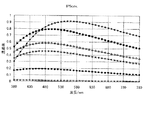
ここで、θ1=θ3=15°とすると、θ2B=120°、θ2W=75°となる。この液晶表示素子において、波長550nmにおけるリターデーション(Δnd)を液晶層1、位相差板2,3ともに、275nmとした場合における黒レベル、白レベルの分光透過率は、図2に示すように、広い波長帯域に亘って平坦な特性を示している。なお、ここで、位相差板2,3としては、ポリカーボネイト(Polycarbonate)延伸フィルムを用いた。
【0022】
位相差板2,3のリターデーション(Δnd)は、概ね、液晶層1のリターデーション(Δnd)に等しく設定する。位相差板2,3と液晶層1のリターデーション(Δnd)がずれると、図3に示すように、黒レベルの透過率が上昇する。この図3では、液晶層1のリターデーション(Δnd)のみを変化させた場合の黒レベルの分光透過率を示している。すなわち、液晶層1のリターデーション(Δnd)の位相差板2,3のリターデーション(Δnd)に対する比率を0.67乃至1.33の範囲で変化させた場合の黒レベルの分光透過率である。
【0023】
リターデーション(Δnd)の値は、図4に示すように、白レベルに影響する。この図4は、位相差板2,3のリターデーション(Δnd)を、液晶層1及び位相差板2,3のリターデーション(Δnd)を等しく保った状態で変化させた場合の白レベルの分光透過率を示している。
【0024】
白レベルの分光透過率をよりフラットにするには、リターデーション(Δnd)は、波長550nmにおいて、200nm乃至300nm程度の範囲が望ましい。しかし、この値は、フラットにしたい波長帯域に応じて調整すべきものである。
【0025】
また、位相差板2,3及び液晶層1の配向方向は、上述の関係式を満たしており、かつ、0°<θ1≦30°の範囲であることが望ましい。θ1を変化させると、図5に示すように、白レベルの分光透過率が変化する。
【0026】
この液晶表示素子においては、中間調表示については完全な補償とはならないものの、従来品に比較すれば、図6に示すように、電圧を変化させていったときの分光透過率について改善が見られる。すなわち、青側の波長帯域おいて、透過率の逆転現象が発生していない。
【0027】
なお、角度設定については、入射偏光板4の吸収軸を基準にとっても同様の結果が得られる。
【0028】
次に、視野角については、位相差板2,3として一軸性のものを使うと、視野角が大きくなるにつれて、位相差が変化することとなる。位相差が変化すると、図7に示すように、黒レベルの上昇が起こる。また、白レベルについても、図8に示すように、レベルが変化する。図7は、一軸性の位相差板を使った場合の波長550nmにおける黒レベルと、白レベルについての、方位角0°(水平)、45°、90°(垂直)、135°での波長550nmにおける透過率の視野角に対する特性を示している。なお、偏光板としては、「日東電工G1220DU」を用いた。
【0029】
本発明に係る液晶表示素子においては、このような視野角についての特性を改善するため、二軸性の位相差板を用いている。すなわち、厚さ方向の屈折率をnz、遅相軸屈折率をns、進相軸屈折率をnfとして、以下の条件が満たされている。
【0030】
(ns−nz)/(ns−nf)=0.5
この条件が満たされているときには、視野角が大きくなったときでも、図8に示すように、位相差が補償される。なお、この条件が満たされていることは、位相差板が二軸性であることに対応しており、この値が1であることは、位相差板が一軸性であることに対応する。図8は、この条件を満たすような二軸性の位相差板を使ったときの波長550nmにおける黒レベルと、白レベルについての、方位角0°(水平)、45°、90°(垂直)、135°での波長550nmにおける透過率の視野角に対する特性を示している。また、この条件が満たされている場合において、視野角が変化したときの色度変化は、図9乃至図12に示すように、極めて少ないものとなっている。これら図9乃至図12は、方位角0°(水平)、45°、90°(垂直)、135°について、それぞれ、視野角を0°から80°まで変化させたときの色度変化を示している。なお、偏光板としては、「日東電工G1220DU」を用いた。
【0031】
〔第2の実施の形態〕
この液晶表示素子において、黒レベルの特性をさらに改善するには、以下の条件が満足されていることが望ましい。
【0032】
(ns−nz)/(ns−nf)<0.5
また、一般的なIPSでは、電圧を十分印加できないので、白レベルでは、実効的リターデーション(Δnd)は黒レベルの80%程度に低下し、さらに、実効的方位変化は、30°程度である。この状態では、白レベルにおいても、以下の条件が満足されていることが望ましい。
【0033】
(ns−nz)/(ns−nf)<0.5
ここで、第1の実施の形態と同じ構成で、以下の条件が満足されているものとする。
【0034】
(ns−nz)/(ns−nf)=0.2
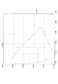
この場合においては、図13の「等コントラストコントア図」及び図14の「白レベルの等色差コントア図」に示すように、図15の従来の液晶表示素子の「等コントラストコントア図」及び図16の従来の液晶表示素子の「白レベルの等色差コントア図」に比較して、視野角が広くなっていることがわかる。ここで、「等コントラストコントア図」については、コントラストが100:1以上となる範囲を示している。また、「等色差コントア図」においては、L*u*V*表色系において、色差が5jnd以内である範囲を示している。
【0035】
〔第3の実施の形態〕
この実施の形態においては、図17に示すように、第1の位相差板2を液晶層1の片側に白レベルの分光透過率の改善の目的で1枚配置する。第2の位相差板3については視野角を補償するためにある。位相差板2,3の配置は、図17に示すように、両側に各1枚ずつ配置する構成と、図18に示すように、液晶層1の片側に2枚を配置する構成とが考えられる。
【0036】
第1の位相差板2の遅相軸と入射偏光板4の透過軸との角度をθ1、第2の位相差板3の遅相軸と入射偏光板4の透過軸との角度をθ3、液晶層1のダイレクタ方位は黒レベル(一般的には電圧無印加時)でθ2B、白レベルでθ2Wとする。ここで、以下の条件が成立している。
【0037】
θ2B=θ1+90°
θ2W=θ1+45°
したがって、θ1=22.5°とすると、θ2B=112.5°、θ2W=67.5°となる。波長550nmにおいて、液晶層1、位相差板2,3ともに、リターデーション(Δnd)を275nmとした場合の黒レベル、白レベルの分光透過率は、図19に示すように、略々フラットな特性になっている。なお、位相差板2,3としては、ポリカーボネイト(Polycarbonate)延伸フィルムを用いた。
【0038】
この実施の形態において、位相差板2,3のリターデーション(Δnd)は、第1の実施の形態と同様に、概ね、液晶層1のリターデーション(Δnd)に等しく設定する。位相差板2,3と液晶層1のリターデーション(Δnd)がずれると、図20に示すように、黒レベルの透過率が上昇する。図20は、液晶層1のリターデーション(Δnd)のみを変化させた場合の黒レベルの分光透過率を示しており、液晶層1のリターデーション(Δnd)の位相差板2,3のリターデーション(Δnd)に対する比率を0.67乃至1.33の範囲で変化させた場合のものである。なお、ここでは、θ1=22.5°、θ2B=112.5°、θ2W=67.5°となっている。
【0039】
リターデーション(Δnd)の値は、図21に示すように、白レベルにも影響する。図21は、位相差板2,3のリターデーション(Δnd)を液晶層1のリターデーション(Δnd)に対して等しく保ちつつ変化させた場合の白レベルの分光透過率を示している。ここでは、θ1=22.5°、θ2B=112.5°、θ2W=67.5°となっている。白レベルの分光透過率をフラットにするには、リターデーション(Δnd)は、波長550nmにおいて、200nm乃至300nm程度の範囲が望ましいが、フラットにしたい波長帯域に応じて調整すべきものである。
【0040】
位相差板2,3及び液晶層1の配向方向は、上述の関係式を満たしており、かつ、0<θ1≦30°の範囲であることが望ましい。θ1を変化させた場合には、図22に示すように、白レベルの分光透過率が変化するが、ここでは、θ1=22.5°の場合が最もフラットな特性を示している。ここでは、リターデーション(Δnd)は、波長550nmにおいて、液晶層1及び位相差板2,3ともに275nmとしている。
【0041】
ところで、この液晶表示素子においては、視野角特性を改善するために、図17に示すように、第2の位相差板3を用いている。第1の実施の形態におけると同様に、位相差板の屈折率について、以下の条件が成立しているものとする。
【0042】
(ns−nz)/(ns−nf)=0.5
そして、θ3=0°とする。この場合には、図23に示すように、波長550nmにおける黒レベル及び白レベルの方位角0°、45°、90°、135°についての透過率視野角特性は良好なものとなっている。また、視野角による色度変化についても、図24乃至図27に示すように、良好な特性となっている。これら図24乃至図27は、方位角0°(水平)、45°、90°(垂直)、135°について、それぞれ、視野角を0°から80°まで変化させたときの色度変化を示している。ここでも、偏光板としては、日東電工G1220DUを用いた。
【0043】
さらに、図18に示すように、第1及び第2の位相差板2,3を液晶層1の片側に配置した場合において、θ3=90°とする。この場合には、図28に示すように、波長550nmにおける黒レベル及び白レベルの方位角0°、45°、90°、135°についての透過率視野角特性は良好なものとなっている。また、視野角による色度変化についても、図29乃至図32に示すように、良好な特性となっている。これら図29乃至図32は、方位角0°(水平)、45°、90°(垂直)、135°について、それぞれ、視野角を0°から80°まで変化させたときの色度変化を示している。ここでも、偏光板としては、日東電工G1220DUを用いた。
【0044】
【発明の効果】
上述のように、本発明に係る液晶表示素子は、いわゆるインプレーンスイッチングモードの液晶表示素子であって、液晶層の両側または片側に配置される位相差板として、二軸性のものを用いることにより、分光透過率の改善、中間調表示における透過率の逆転現象の防止、大きな視野角における色度変化の抑制、コントラストの改善を図っている。
【0045】
すなわち、本発明は、分光透過率が良好であり、中間調表示においても透過率の逆転現象が起こることがなく、さらに、大きな視野角においての色度変化が抑えられ、良好なコントラストにより画像表示を行うことができる液晶表示素子を提供することができるものである。
【図面の簡単な説明】
【図1】本発明に係る液晶表示素子の第1及び第2の実施の形態における構成を示す斜視図である。
【図2】上記液晶表示素子の黒レベル及び白レベルの分光特性を示すグラフである。
【図3】上記液晶表示素子において液晶層のリターデーションがずれた場合の黒レベルの分光特性を示すグラフである。
【図4】上記液晶表示素子におけるリターデーションの値の白レベルの分光特性への影響を示すグラフである。
【図5】上記液晶表示素子における位相差板の遅相軸方位の変化の白レベルの分光特性への影響を示すグラフである。
【図6】上記液晶表示素子における中間調表示についての分光透過率を示すグラフである。
【図7】液晶表示素子において位相差板として一軸性のものを使った場合の視野角に対する黒レベルの変化を示すグラフである。
【図8】液晶表示素子において位相差板として一軸性のものを使った場合の視野角に対する白レベルの変化を示すグラフである。
【図9】本発明に係る液晶表示素子において方位角0°(水平)について視野角を0°から80°まで変化させたときの色度変化を示す色度図である。
【図10】上記液晶表示素子において方位角45°について視野角を0°から80°まで変化させたときの色度変化を示す色度図である。
【図11】上記液晶表示素子において方位角90°(垂直)について視野角を0°から80°まで変化させたときの色度変化を示す色度図である。
【図12】上記液晶表示素子において方位角135°について視野角を0°から80°まで変化させたときの色度変化を示す色度図である。
【図13】上記液晶表示素子における等コントラストコントア図である。
【図14】上記液晶表示素子における白レベルの等色差コントア図である。
【図15】従来の液晶表示素子における等コントラストコントア図である。
【図16】上記従来の液晶表示素子における白レベルの等色差コントア図である。
【図17】本発明に係る液晶表示素子の第3の実施の形態において位相差板を液晶層の両側に配置した構成を示す斜視図である。
【図18】上記液晶表示素子の第3の実施の形態において位相差板を液晶層の片側に配置した構成を示す斜視図である。
【図19】上記液晶表示素子の黒レベル及び白レベルの分光特性を示すグラフである。
【図20】上記液晶表示素子において液晶層のリターデーションがずれた場合の黒レベルの分光特性を示すグラフである。
【図21】上記液晶表示素子におけるリターデーションの値の白レベルの分光特性への影響を示すグラフである。
【図22】上記液晶表示素子における位相差板の遅相軸方位の変化の白レベルの分光特性への影響を示すグラフである。
【図23】上記液晶表示素子においてθ3=0°とした場合の視野角に対する白レベル及び黒レベルの変化を示すグラフである。
【図24】上記液晶表示素子において方位角0°(水平)について視野角を0°から80°まで変化させたときの色度変化を示す色度図である。
【図25】上記液晶表示素子において方位角45°について視野角を0°から80°まで変化させたときの色度変化を示す色度図である。
【図26】上記液晶表示素子において方位角90°(垂直)について視野角を0°から80°まで変化させたときの色度変化を示す色度図である。
【図27】上記液晶表示素子において方位角135°について視野角を0°から80°まで変化させたときの色度変化を示す色度図である。
【図28】上記液晶表示素子においてθ3=90°とした場合の視野角に対する白レベル及び黒レベルの変化を示すグラフである。
【図29】上記液晶表示素子において方位角0°(水平)について視野角を0°から80°まで変化させたときの色度変化を示す色度図である。
【図30】上記液晶表示素子において方位角45°について視野角を0°から80°まで変化させたときの色度変化を示す色度図である。
【図31】上記液晶表示素子において方位角90°(垂直)について視野角を0°から80°まで変化させたときの色度変化を示す色度図である。
【図32】上記液晶表示素子において方位角135°について視野角を0°から80°まで変化させたときの色度変化を示す色度図である。
【図33】従来の液晶表示素子における黒レベル及び白レベルの分光特性を示すグラフである。
【図34】上記従来の液晶表示素子における中間調表示についての分光透過率を示すグラフである。
【図35】上記従来の液晶表示素子において方位角0°(水平)について視野角を0°から80°まで変化させたときの色度変化を示す色度図である。
【図36】上記従来の液晶表示素子において方位角45°について視野角を0°から80°まで変化させたときの色度変化を示す色度図である。
【図37】上記従来の液晶表示素子において方位角90°(垂直)について視野角を0°から80°まで変化させたときの色度変化を示す色度図である。
【図38】上記従来の液晶表示素子において方位角135°について視野角を0°から80°まで変化させたときの色度変化を示す色度図である。
【符号の説明】
1 液晶層、2 第1の位相差板、3 第2の位相差板、4 入射偏光板、5
出射偏光板[0001]
BACKGROUND OF THE INVENTION
The present invention relates to a so-called in-plane switching mode liquid crystal display element that displays an image by forming an electric field in a direction parallel to a substrate between a pixel electrode and a common electrode.
[0002]
[Prior art]
2. Description of the Related Art Conventionally, a so-called in-plane switching mode liquid crystal display element that displays an image by forming an electric field in a direction parallel to a substrate between a pixel electrode and a common electrode has been proposed. This in-plane switching mode is known to provide a wider viewing angle than the TN mode.
[0003]
Such a liquid crystal display element includes a pair of substrates, a liquid crystal layer provided between the substrates, first and second polarizing plates disposed between the substrates, and the polarizing plate and each substrate. The first and second retardation plates are provided between the first and second retardation plates.
[0004]
In this liquid crystal display element, the alignment direction of the polarizing plate and the liquid crystal layer is set so that the initial alignment is set to black display when no voltage is applied between the electrodes. The orientation direction of the layers is generally rotated by 45 ° to display white.
[0005]
The director distribution in the liquid crystal layer in white display is twisted, but optically functions as a λ / 2 plate (half-wave plate). The director distribution is twisted when the director near the substrate does not move much. When functioning as a λ / 2 plate, the maximum transmittance is obtained when the effective retardation (Δnd) is λ / 2 in the 45 ° orientation.
[0006]
[Problems to be solved by the invention]
By the way, in the liquid crystal display element as described above, for example, when the retardation (Δnd) is λ / 2 at a wavelength of 550 nm, as shown in FIG. 33, it functions as a λ / 2 plate. In the vicinity of the wavelength of 550 nm and at a wavelength distance from 550 nm, the transmittance decreases. That is, since the transmittance T is expressed by the following equation, the transmittance T is reduced except for a predetermined wavelength.
[0007]
T = sin2π (Δnd / λ)
Further, due to the twist of the director distribution in the liquid crystal layer in the white display, the transmittance T is further reduced as shown in the following formula, particularly in a low voltage state (sin 22φ corresponds to the influence of the twist of the director distribution). .
[0008]
T = sin22φsin2π (Δnd / λ)
In the halftone, as shown in FIG. 34, when the voltage is changed, the reversal of the transmittance occurs at the wavelength on the blue side (band of about 460 nm or less).
[0009]
Furthermore, as shown in FIGS. 35 to 38, when the viewing angle is large, chromaticity change occurs. FIGS. 35 to 38 show changes in chromaticity when the viewing angle is changed from 0 ° to 80 ° for azimuth angles of 0 ° (horizontal), 45 °, 90 ° (vertical), and 135 °, respectively. ing. It can be seen that for azimuth angles of 45 ° and 135 °, a considerably large change in chromaticity occurs. In obtaining the data shown in FIGS. 35 to 38, “Nitto Denko G1220DU” is used as a polarizing plate, and a C light source is used as a light source.
[0010]
Therefore, the present invention has been proposed in view of the above-described circumstances, has a good spectral transmittance, does not cause a reversal of transmittance even in a halftone display, and has a large viewing angle. The liquid crystal display element which can suppress the chromaticity change of this and can perform image display by favorable contrast is intended to be provided.
[0011]
[Means for Solving the Problems]
In order to solve the above-described problems, a liquid crystal display element according to the present invention includes a pair of substrates, at least one of which is transparent, a pixel electrode group, and a common electrode group. An electrode group for forming a pixel region, a liquid crystal layer provided between the substrates, first and second polarizing plates disposed between the substrates, and the first polarizing plate and each substrate. A first retardation plate disposed between the second polarizing plate and a second retardation plate disposed between each substrate and the first and second retardation plates; the above liquid crystal layer, in which retardation displays an image by equal to each other, the electric field in the direction parallel to the substrate between the pixel electrode and the common electrode through the electrode group is formed.
[0012]
In this liquid crystal display element, with reference to the orientation of the first polarizing plate, the angle formed by the slow axis of the first retardation plate is θ1, the angle formed by the slow axis of the liquid crystal layer is θ2, and the above The angle formed by the slow axis of the second retardation plate is θ3, and for the birefringence of the retardation plate, the slow axis refractive index is ns, the fast axis refractive index is nf, and the refractive index in the thickness direction is nz. When (ns−nz) / (ns−nf) ≦ 0.5θ1 = θ3 holds, when the display element is at the white level , θ2 = 2 × θ1 + 45 ° holds, and when the display element is at the black level , Θ2 = 2 × θ1 + 90 ° is satisfied.
[0013]
In the liquid crystal display element according to the present invention, (ns−nz) / (ns−nf) ≦ 0.5θ3 = 0 ° is established , and θ2 = θ1 + 45 ° is established when the display element is at the white level. When the display element is at a black level, the condition of θ2 = θ1 + 90 ° is satisfied.
[0014]
Further, in the liquid crystal display element according to the present invention, (ns−nz) / (ns−nf) ≦ 0.5θ3 = 90 ° is established , and θ2 = θ1 + 45 ° is established when the display element is at the white level. When the display element is at a black level, the condition of θ2 = θ1 + 90 ° is satisfied.
[0016]
DETAILED DESCRIPTION OF THE INVENTION
Embodiments of the present invention will be described below with reference to the drawings.
[0017]
As shown in FIG. 1, the liquid crystal display element according to the present invention includes a liquid crystal layer 1, first and
[0018]
In this liquid crystal display element, the liquid crystal layer 1 is provided between a pair of substrates (not shown). At least one of these substrates is formed to be transparent. The substrate is provided with an electrode group including a pixel electrode group and a common electrode group. In this electrode group, pixel regions are formed in a matrix on the substrate by each pixel electrode and each common electrode. The liquid crystal display element is a so-called in-plane switching mode liquid crystal display element that performs image display by forming an electric field in a direction parallel to the substrate between the pixel electrode and the common electrode.
[0019]
In this liquid crystal display element, the incident polarizing plate 4 and the outgoing polarizing plate 5 are arranged in a crossed Nicols relationship. The orientation directions of the polarizing plates 4 and 5 and the liquid crystal layer 1 are set so that the initial orientation is black when no voltage is applied between the pixel electrode and the common electrode, and an electric field is applied. Sometimes, the alignment direction of the liquid crystal layer 1 is rotated by 45 ° to display white. The director distribution in the liquid crystal layer 1 in white display is twisted due to the fact that the director in the vicinity of the substrate does not move so much, but optically functions as a λ / 2 plate (half-wave plate). When the liquid crystal layer 1 functions as a λ / 2 plate, the maximum transmittance is obtained when the effective retardation (Δnd) is λ / 2 in a 45 ° orientation.
[0020]
[First Embodiment]
Using the transmission axis of the incident polarizing plate 4 as a reference, the slow axis directions of the
[0021]
θ1 = θ3
θ2B = θ1 × 2 + 90 °
θ2W = θ1 × 2 + 45 °
Here, when θ1 = θ3 = 15 °, θ2B = 120 ° and θ2W = 75 °. In this liquid crystal display element, when the retardation (Δnd) at a wavelength of 550 nm is 275 nm for both the liquid crystal layer 1 and the
[0022]
The retardation (Δnd) of the
[0023]
The value of retardation (Δnd) affects the white level as shown in FIG. FIG. 4 shows a white level spectrum when the retardation (Δnd) of the
[0024]
In order to make the white level spectral transmittance flatter, the retardation (Δnd) is preferably in the range of about 200 nm to 300 nm at a wavelength of 550 nm. However, this value should be adjusted according to the wavelength band to be flattened.
[0025]
The alignment directions of the
[0026]
In this liquid crystal display element, halftone display is not completely compensated, but as compared with the conventional product, as shown in FIG. 6, the spectral transmittance when the voltage is changed is improved. It is done. That is, the transmittance reversal phenomenon does not occur in the blue wavelength band.
[0027]
As for the angle setting, the same result can be obtained using the absorption axis of the incident polarizing plate 4 as a reference.
[0028]
Next, regarding the viewing angle, if a uniaxial one is used as the
[0029]
In the liquid crystal display element according to the present invention, a biaxial retardation plate is used in order to improve the characteristics with respect to such a viewing angle. That is, the following conditions are satisfied, assuming that the refractive index in the thickness direction is nz, the slow axis refractive index is ns, and the fast axis refractive index is nf.
[0030]
(Ns-nz) / (ns-nf) = 0.5
When this condition is satisfied, the phase difference is compensated as shown in FIG. 8 even when the viewing angle is increased. The fact that this condition is satisfied corresponds to the retardation plate being biaxial, and the value of 1 corresponds to the retardation plate being uniaxial. FIG. 8 shows an azimuth angle of 0 ° (horizontal), 45 °, and 90 ° (vertical) with respect to the black level and the white level at a wavelength of 550 nm when a biaxial retardation plate satisfying this condition is used. , Shows the characteristics of the transmittance with respect to the viewing angle at a wavelength of 550 nm at 135 °. In addition, when this condition is satisfied, the change in chromaticity when the viewing angle changes is extremely small as shown in FIGS. 9 to 12 show changes in chromaticity when the viewing angle is changed from 0 ° to 80 ° for azimuth angles of 0 ° (horizontal), 45 °, 90 ° (vertical), and 135 °, respectively. ing. In addition, “Nitto Denko G1220DU” was used as the polarizing plate.
[0031]
[Second Embodiment]
In this liquid crystal display element, it is desirable that the following conditions are satisfied in order to further improve the black level characteristics.
[0032]
(Ns-nz) / (ns-nf) <0.5
In addition, since a voltage cannot be sufficiently applied in a general IPS, the effective retardation (Δnd) is reduced to about 80% of the black level at the white level, and the effective orientation change is about 30 °. . In this state, it is desirable that the following condition is satisfied even at the white level.
[0033]
(Ns-nz) / (ns-nf) <0.5
Here, it is assumed that the following conditions are satisfied with the same configuration as the first embodiment.
[0034]
(Ns-nz) / (ns-nf) = 0.2
In this case, as shown in the “equal contrast controller diagram” of FIG. 13 and the “equal color difference controller diagram of white level” in FIG. 14, the “equal contrast controller diagram” of the conventional liquid crystal display element in FIG. It can be seen that the viewing angle is wider than the “white level equal color difference controller diagram” of the conventional liquid crystal display element of FIG. Here, the “isocontrast controller diagram” indicates a range where the contrast is 100: 1 or more. Further, the “equal color difference contour diagram” shows a range in which the color difference is within 5 jnd in the L * u * V * color system.
[0035]
[Third Embodiment]
In this embodiment, as shown in FIG. 17, one
[0036]
The angle between the slow axis of the
[0037]
θ2B = θ1 + 90 °
θ2W = θ1 + 45 °
Therefore, when θ1 = 22.5 °, θ2B = 112.5 ° and θ2W = 67.5 °. When the retardation (Δnd) is 275 nm for both the liquid crystal layer 1 and the
[0038]
In this embodiment, the retardation (Δnd) of the
[0039]
The retardation (Δnd) value also affects the white level as shown in FIG. FIG. 21 shows the spectral transmittance of the white level when the retardation (Δnd) of the
[0040]
The alignment directions of the
[0041]
Incidentally, in this liquid crystal display element, the
[0042]
(Ns-nz) / (ns-nf) = 0.5
Then, θ3 = 0 °. In this case, as shown in FIG. 23, the transmittance viewing angle characteristics with respect to the azimuth angles 0 °, 45 °, 90 °, and 135 ° of the black level and the white level at a wavelength of 550 nm are good. Further, the change in chromaticity depending on the viewing angle also has good characteristics as shown in FIGS. 24 to 27 show changes in chromaticity when the viewing angle is changed from 0 ° to 80 ° for azimuth angles of 0 ° (horizontal), 45 °, 90 ° (vertical), and 135 °, respectively. ing. Again, Nitto Denko G1220DU was used as the polarizing plate.
[0043]
Further, as shown in FIG. 18, when the first and
[0044]
【The invention's effect】
As described above, the liquid crystal display element according to the present invention is a so-called in-plane switching mode liquid crystal display element, and a biaxial one is used as a retardation plate disposed on both sides or one side of the liquid crystal layer. Thus, the spectral transmittance is improved, the reverse phenomenon of the transmittance in halftone display is prevented, the chromaticity change is suppressed at a large viewing angle, and the contrast is improved.
[0045]
That is, according to the present invention, the spectral transmittance is good, the inversion phenomenon of the transmittance does not occur even in the halftone display, the chromaticity change at a large viewing angle is suppressed, and the image is displayed with a good contrast. It is possible to provide a liquid crystal display element capable of performing the above.
[Brief description of the drawings]
FIG. 1 is a perspective view showing a configuration of a liquid crystal display element according to the present invention in first and second embodiments.
FIG. 2 is a graph showing spectral characteristics of a black level and a white level of the liquid crystal display element.
FIG. 3 is a graph showing the spectral characteristics of black level when the retardation of the liquid crystal layer is shifted in the liquid crystal display element.
FIG. 4 is a graph showing the influence of retardation value on spectral characteristics of white level in the liquid crystal display element.
FIG. 5 is a graph showing the influence of the change in the slow axis direction of the retardation plate in the liquid crystal display element on the spectral characteristics of the white level.
FIG. 6 is a graph showing spectral transmittance for halftone display in the liquid crystal display element.
FIG. 7 is a graph showing a change in black level with respect to a viewing angle when a uniaxial retardation plate is used in a liquid crystal display element.
FIG. 8 is a graph showing a change in white level with respect to a viewing angle when a uniaxial retardation plate is used in a liquid crystal display element.
FIG. 9 is a chromaticity diagram showing a change in chromaticity when the viewing angle is changed from 0 ° to 80 ° at an azimuth angle of 0 ° (horizontal) in the liquid crystal display element according to the present invention.
FIG. 10 is a chromaticity diagram showing a change in chromaticity when the viewing angle is changed from 0 ° to 80 ° at an azimuth angle of 45 ° in the liquid crystal display element.
FIG. 11 is a chromaticity diagram showing a change in chromaticity when the viewing angle is changed from 0 ° to 80 ° at an azimuth angle of 90 ° (vertical) in the liquid crystal display element.
FIG. 12 is a chromaticity diagram showing a change in chromaticity when the viewing angle is changed from 0 ° to 80 ° with respect to an azimuth angle of 135 ° in the liquid crystal display element.
FIG. 13 is an iso-contrast contour diagram in the liquid crystal display element.
FIG. 14 is a white level equal color difference contour diagram in the liquid crystal display element.
FIG. 15 is an iso-contrast contour diagram in a conventional liquid crystal display element.
FIG. 16 is a white level equal color difference contour diagram in the conventional liquid crystal display device.
FIG. 17 is a perspective view showing a configuration in which retardation plates are arranged on both sides of a liquid crystal layer in a third embodiment of a liquid crystal display element according to the present invention.
FIG. 18 is a perspective view showing a configuration in which a retardation plate is arranged on one side of a liquid crystal layer in the third embodiment of the liquid crystal display element.
FIG. 19 is a graph showing spectral characteristics of a black level and a white level of the liquid crystal display element.
FIG. 20 is a graph showing the spectral characteristics of the black level when the retardation of the liquid crystal layer is shifted in the liquid crystal display element.
FIG. 21 is a graph showing the influence of the retardation value on the spectral characteristics of the white level in the liquid crystal display element.
FIG. 22 is a graph showing the influence of the change in the slow axis direction of the retardation plate in the liquid crystal display element on the spectral characteristics of the white level.
FIG. 23 is a graph showing changes in white level and black level with respect to a viewing angle when θ3 = 0 ° in the liquid crystal display element.
FIG. 24 is a chromaticity diagram showing a change in chromaticity when the viewing angle is changed from 0 ° to 80 ° at an azimuth angle of 0 ° (horizontal) in the liquid crystal display element.
FIG. 25 is a chromaticity diagram showing a change in chromaticity when the viewing angle is changed from 0 ° to 80 ° at an azimuth angle of 45 ° in the liquid crystal display element.
FIG. 26 is a chromaticity diagram showing a change in chromaticity when the viewing angle is changed from 0 ° to 80 ° at an azimuth angle of 90 ° (vertical) in the liquid crystal display element.
FIG. 27 is a chromaticity diagram showing a change in chromaticity when the viewing angle is changed from 0 ° to 80 ° with respect to an azimuth angle of 135 ° in the liquid crystal display element.
FIG. 28 is a graph showing changes in white level and black level with respect to a viewing angle when θ3 = 90 ° in the liquid crystal display element.
FIG. 29 is a chromaticity diagram showing a change in chromaticity when the viewing angle is changed from 0 ° to 80 ° at an azimuth angle of 0 ° (horizontal) in the liquid crystal display element.
FIG. 30 is a chromaticity diagram showing a change in chromaticity when the viewing angle is changed from 0 ° to 80 ° at an azimuth angle of 45 ° in the liquid crystal display element.
FIG. 31 is a chromaticity diagram showing a change in chromaticity when the viewing angle is changed from 0 ° to 80 ° at an azimuth angle of 90 ° (vertical) in the liquid crystal display element.
FIG. 32 is a chromaticity diagram showing a change in chromaticity when the viewing angle is changed from 0 ° to 80 ° with respect to an azimuth angle of 135 ° in the liquid crystal display element.
FIG. 33 is a graph showing spectral characteristics of a black level and a white level in a conventional liquid crystal display element.
FIG. 34 is a graph showing spectral transmittance for halftone display in the conventional liquid crystal display element.
FIG. 35 is a chromaticity diagram showing changes in chromaticity when the viewing angle is changed from 0 ° to 80 ° at an azimuth angle of 0 ° (horizontal) in the conventional liquid crystal display device.
FIG. 36 is a chromaticity diagram showing a change in chromaticity when the viewing angle is changed from 0 ° to 80 ° at an azimuth angle of 45 ° in the conventional liquid crystal display element.
FIG. 37 is a chromaticity diagram showing a change in chromaticity when the viewing angle is changed from 0 ° to 80 ° at an azimuth angle of 90 ° (vertical) in the conventional liquid crystal display device.
FIG. 38 is a chromaticity diagram showing a change in chromaticity when the viewing angle is changed from 0 ° to 80 ° with an azimuth angle of 135 ° in the conventional liquid crystal display device.
[Explanation of symbols]
DESCRIPTION OF SYMBOLS 1 Liquid crystal layer, 2 1st phase difference plate, 2nd phase difference plate, 4 Incident polarizing plate, 5
Output polarizing plate
Claims (3)
画素電極群とコモン電極群とからなり、各画素電極とコモン電極とにより、上記基板上にマトリクス状に画素領域を形成する電極群と、
上記各基板間に設けられた液晶層と、
上記各基板を挟んで配設された第1及び第2の偏光板と、
上記第1の偏光板と上記各基板との間に配設された第1の位相差板と、
上記第2の偏光板と上記各基板との間に配設された第2の位相差板と
を備え、
上記第1及び第2の位相差板と上記液晶層とは、リターデーションが互いに等しく、
上記第1の偏光板の方位を基準として、上記第1の位相差板の遅相軸がなす角度をθ1、上記液晶層の遅相軸がなす角度をθ2、上記第2の位相差板の遅相軸がなす角度をθ3とするとき、
θ1=θ3
が成立し、表示素子が白レベルのときには、
θ2=2xθ1+45°
が成立し、表示素子が黒レベルのときには、
θ2=2xθ1+90°
が成立し、さらに、上記位相差板の複屈折率について、遅相軸屈折率をns、進相軸屈折率をnf、厚さ方向の屈折率をnzとするとき、
(ns−nz)/(ns−nf)≦0.5
という条件が満足され、
上記電極群を介して上記画素電極と上記コモン電極との間に上記基板に平行な方向の電界が形成されることにより、画像を表示することを特徴とする液晶表示素子。A pair of substrates at least one of which is transparent;
An electrode group comprising a pixel electrode group and a common electrode group, each pixel electrode and the common electrode forming a pixel region in a matrix on the substrate;
A liquid crystal layer provided between the substrates,
A first polarizing plate and a second polarizing plate disposed across the substrates;
A first retardation plate disposed between the first polarizing plate and each of the substrates;
A second retardation plate disposed between the second polarizing plate and each of the substrates,
It said the first and second phase difference plate and the liquid crystal layer, the retardation is equal to each other,
With reference to the orientation of the first polarizer, the angle formed by the slow axis of the first retardation plate is θ1, the angle formed by the slow axis of the liquid crystal layer is θ2, and the second retardation plate When the angle formed by the slow axis is θ3,
θ1 = θ3
When the display element is at the white level ,
θ2 = 2xθ1 + 45 °
When the display element is at the black level,
θ2 = 2xθ1 + 90 °
Further, for the birefringence of the retardation plate, when the slow axis refractive index is ns, the fast axis refractive index is nf, and the refractive index in the thickness direction is nz,
(Ns-nz) / (ns-nf) ≦ 0.5
Is satisfied,
A liquid crystal display element that displays an image by forming an electric field in a direction parallel to the substrate between the pixel electrode and the common electrode through the electrode group.
画素電極群とコモン電極群とからなり、各画素電極とコモン電極とにより、上記基板上にマトリクス状に画素領域を形成する電極群と、
上記各基板間に設けられた液晶層と、
上記各基板を挟んで配設された第1及び第2の偏光板と、
上記第1の偏光板と上記各基板との間に配設された第1の位相差板と、
上記第2の偏光板と上記各基板との間に配設された第2の位相差板と
を備え、
上記第1及び第2の位相差板と上記液晶層とは、リターデーションが互いに等しく、
上記第1の偏光板の方位を基準として、上記第1の位相差板の遅相軸がなす角度をθ1、上記液晶層の遅相軸がなす角度をθ2、上記第2の位相差板の遅相軸がなす角度をθ3とするとき、
θ3=0°
が成立し、表示素子が白レベルのときには、
θ2=θ1+45°
が成立し、表示素子が黒レベルのときには、
θ2=θ1+90°
が成立し、さらに、上記位相差板の複屈折率について、遅相軸屈折率をns、進相軸屈折率をnf、厚さ方向の屈折率をnzとするとき、
(ns−nz)/(ns−nf)≦0.5
という条件が満足され、
上記電極群を介して上記画素電極と上記コモン電極との間に上記基板に平行な方向の電界が形成されることにより、画像を表示する
ことを特徴とする液晶表示素子。A pair of substrates at least one of which is transparent;
An electrode group comprising a pixel electrode group and a common electrode group, each pixel electrode and the common electrode forming a pixel region in a matrix on the substrate;
A liquid crystal layer provided between the substrates,
A first polarizing plate and a second polarizing plate disposed across the substrates;
A first retardation plate disposed between the first polarizing plate and each of the substrates;
A second retardation plate disposed between the second polarizing plate and each of the substrates,
It said the first and second phase difference plate and the liquid crystal layer, the retardation is equal to each other,
With reference to the orientation of the first polarizer, the angle formed by the slow axis of the first retardation plate is θ1, the angle formed by the slow axis of the liquid crystal layer is θ2, and the second retardation plate When the angle formed by the slow axis is θ3,
θ3 = 0 °
When the display element is at the white level ,
θ2 = θ1 + 45 °
When the display element is at the black level,
θ2 = θ1 + 90 °
Further, for the birefringence of the retardation plate, when the slow axis refractive index is ns, the fast axis refractive index is nf, and the refractive index in the thickness direction is nz,
(Ns-nz) / (ns-nf) ≦ 0.5
Is satisfied,
A liquid crystal display element, wherein an image is displayed by forming an electric field in a direction parallel to the substrate between the pixel electrode and the common electrode through the electrode group.
画素電極群とコモン電極群とからなり、各画素電極とコモン電極とにより、上記基板上にマトリクス状に画素領域を形成する電極群と、
上記各基板間に設けられた液晶層と、
上記各基板を挟んで配設された第1及び第2の偏光板と、
上記第1の偏光板と上記各基板との間に配設された第1の位相差板及び第2の位相差板と
を備え、
上記第1及び第2の位相差板と上記液晶層とは、リターデーションが互いに等しく、
上記第1の偏光板の方位を基準として、上記第1の位相差板の遅相軸がなす角度をθ1、上記液晶層の遅相軸がなす角度をθ2、上記第2の位相差板の遅相軸がなす角度をθ3とするとき、
θ3=90°
が成立し、表示素子が白レベルのときには、
θ2=θ1+45°
が成立し、表示素子が黒レベルのときには、
θ2=θ1+90°
が成立し、さらに、上記位相差板の複屈折率について、遅相軸屈折率をns、進相軸屈折率をnf、厚さ方向の屈折率をnzとするとき、
(ns−nz)/(ns−nf)≦0.5
という条件が満足され、
上記電極群を介して上記画素電極と上記コモン電極との間に上記基板に平行な方向の電界が形成されることにより、画像を表示することを特徴とする液晶表示素子。A pair of substrates at least one of which is transparent;
An electrode group comprising a pixel electrode group and a common electrode group, each pixel electrode and the common electrode forming a pixel region in a matrix on the substrate;
A liquid crystal layer provided between the substrates,
A first polarizing plate and a second polarizing plate disposed across the substrates;
A first retardation plate and a second retardation plate disposed between the first polarizing plate and each of the substrates ;
With
It said the first and second phase difference plate and the liquid crystal layer, the retardation is equal to each other,
Using the orientation of the first polarizing plate as a reference, the angle formed by the slow axis of the first retardation plate is θ1, the angle formed by the slow axis of the liquid crystal layer is θ2, and the second retardation plate When the angle formed by the slow axis is θ3,
θ3 = 90 °
When the display element is at the white level ,
θ2 = θ1 + 45 °
When the display element is at the black level,
θ2 = θ1 + 90 °
Further, for the birefringence of the retardation plate, when the slow axis refractive index is ns, the fast axis refractive index is nf, and the refractive index in the thickness direction is nz,
(Ns-nz) / (ns-nf) ≦ 0.5
Is satisfied,
A liquid crystal display element that displays an image by forming an electric field in a direction parallel to the substrate between the pixel electrode and the common electrode through the electrode group.
Priority Applications (1)
| Application Number | Priority Date | Filing Date | Title |
|---|---|---|---|
| JP2000056073A JP4441971B2 (en) | 2000-02-28 | 2000-02-28 | Liquid crystal display element |
Applications Claiming Priority (1)
| Application Number | Priority Date | Filing Date | Title |
|---|---|---|---|
| JP2000056073A JP4441971B2 (en) | 2000-02-28 | 2000-02-28 | Liquid crystal display element |
Publications (2)
| Publication Number | Publication Date |
|---|---|
| JP2001242462A JP2001242462A (en) | 2001-09-07 |
| JP4441971B2 true JP4441971B2 (en) | 2010-03-31 |
Family
ID=18577093
Family Applications (1)
| Application Number | Title | Priority Date | Filing Date |
|---|---|---|---|
| JP2000056073A Expired - Fee Related JP4441971B2 (en) | 2000-02-28 | 2000-02-28 | Liquid crystal display element |
Country Status (1)
| Country | Link |
|---|---|
| JP (1) | JP4441971B2 (en) |
Families Citing this family (18)
| Publication number | Priority date | Publication date | Assignee | Title |
|---|---|---|---|---|
| JP4328205B2 (en) * | 2001-10-04 | 2009-09-09 | 富士フイルム株式会社 | Transmission type liquid crystal display device |
| JP4002433B2 (en) | 2001-12-27 | 2007-10-31 | Nec液晶テクノロジー株式会社 | Active matrix type liquid crystal display device |
| US7289179B2 (en) | 2002-11-08 | 2007-10-30 | Samsung Electronics Co., Ltd. | Liquid crystal display |
| JP4253259B2 (en) * | 2003-08-15 | 2009-04-08 | 富士フイルム株式会社 | Liquid crystal display |
| JP4564795B2 (en) * | 2003-09-30 | 2010-10-20 | 株式会社日立製作所 | Liquid crystal display |
| JP4882375B2 (en) | 2003-11-21 | 2012-02-22 | 日本ゼオン株式会社 | Liquid crystal display |
| TWI371620B (en) * | 2003-11-21 | 2012-09-01 | Zeon Corp | Liquid crystal display apparatus (1) |
| JP4883518B2 (en) | 2003-12-12 | 2012-02-22 | Nltテクノロジー株式会社 | Liquid crystal display |
| JP4708710B2 (en) | 2004-01-07 | 2011-06-22 | Nec液晶テクノロジー株式会社 | Liquid crystal display device |
| JP4693062B2 (en) * | 2004-03-26 | 2011-06-01 | 日東電工株式会社 | IPS mode liquid crystal display device |
| WO2005116741A1 (en) | 2004-05-26 | 2005-12-08 | Nitto Denko Corporation | Liquid crystal display |
| US7619818B2 (en) | 2004-05-26 | 2009-11-17 | Nitto Denko Corporation | Elliptically polarizing plate and image display |
| JPWO2006035635A1 (en) * | 2004-09-27 | 2008-05-15 | 日本ゼオン株式会社 | Liquid crystal display |
| JP4708756B2 (en) * | 2004-10-05 | 2011-06-22 | Nec液晶テクノロジー株式会社 | Liquid crystal display device |
| JP4642493B2 (en) | 2005-01-31 | 2011-03-02 | Nec液晶テクノロジー株式会社 | Liquid crystal display device |
| US7605895B2 (en) * | 2005-06-14 | 2009-10-20 | Lg Chem, Ltd. | IPS mode liquid crystal display using two sheets of biaxial negative retardation film and a plate |
| JP2007079115A (en) | 2005-09-14 | 2007-03-29 | Nec Lcd Technologies Ltd | Pair of polarizing plates, and liquid crystal display device |
| KR100789681B1 (en) | 2005-09-14 | 2008-01-02 | 엔이씨 엘씨디 테크놀로지스, 엘티디. | Lcd device having an improved viewing angle characteristic |
-
2000
- 2000-02-28 JP JP2000056073A patent/JP4441971B2/en not_active Expired - Fee Related
Also Published As
| Publication number | Publication date |
|---|---|
| JP2001242462A (en) | 2001-09-07 |
Similar Documents
| Publication | Publication Date | Title |
|---|---|---|
| JP2982869B2 (en) | Liquid crystal display | |
| JP4441971B2 (en) | Liquid crystal display element | |
| JP3763401B2 (en) | Liquid crystal display | |
| US6307608B1 (en) | Liquid crystal display having wide viewing angle range | |
| US7440047B2 (en) | Liquid crystal display device and electronic apparatus having two elliptically polarizing plates | |
| KR101293564B1 (en) | Liquid crystal display device | |
| US8310634B2 (en) | Liquid crystal display device comprising a first optical compensating member between the liquid crystal layer and one of the first and second polarizing layers | |
| US20090147193A1 (en) | Liquid crystal display device | |
| JPWO2005015297A1 (en) | Liquid crystal display | |
| US8085370B2 (en) | Single-polarizer reflective bistable twisted nematic (BTN) liquid crystal display device | |
| JPH11311784A (en) | Liquid crystal display device and display | |
| US7295271B2 (en) | Liquid crystal display device and multilayer phase plate | |
| US7973882B2 (en) | Liquid crystal display device | |
| JP2006030688A (en) | Liquid crystal display | |
| US7443473B2 (en) | Optical compensation polarizing film achieving a higher viewing angle | |
| JP2796210B2 (en) | Liquid crystal display | |
| US20060221283A1 (en) | Liquid crystal display device | |
| KR20100024638A (en) | Liquid crystal displayand the manufacturing method thereof | |
| JPH05313159A (en) | Liquid crystal display device | |
| KR20080059832A (en) | Display apparatus | |
| JP4366985B2 (en) | Liquid crystal display | |
| JP2968152B2 (en) | Liquid crystal display | |
| JP2006018185A (en) | Liquid crystal display | |
| JPH06342154A (en) | Liquid crystal display device | |
| KR100720919B1 (en) | a optical film for liquid crystal display |
Legal Events
| Date | Code | Title | Description |
|---|---|---|---|
| A621 | Written request for application examination |
Free format text: JAPANESE INTERMEDIATE CODE: A621 Effective date: 20061031 |
|
| A977 | Report on retrieval |
Free format text: JAPANESE INTERMEDIATE CODE: A971007 Effective date: 20090901 |
|
| A131 | Notification of reasons for refusal |
Free format text: JAPANESE INTERMEDIATE CODE: A131 Effective date: 20090929 |
|
| A521 | Written amendment |
Free format text: JAPANESE INTERMEDIATE CODE: A523 Effective date: 20091120 |
|
| TRDD | Decision of grant or rejection written | ||
| A01 | Written decision to grant a patent or to grant a registration (utility model) |
Free format text: JAPANESE INTERMEDIATE CODE: A01 Effective date: 20091222 |
|
| A01 | Written decision to grant a patent or to grant a registration (utility model) |
Free format text: JAPANESE INTERMEDIATE CODE: A01 |
|
| A61 | First payment of annual fees (during grant procedure) |
Free format text: JAPANESE INTERMEDIATE CODE: A61 Effective date: 20100104 |
|
| FPAY | Renewal fee payment (prs date is renewal date of database) |
Free format text: PAYMENT UNTIL: 20130122 Year of fee payment: 3 |
|
| LAPS | Cancellation because of no payment of annual fees |