JP4439685B2 - Memory data correction circuit - Google Patents
Memory data correction circuit Download PDFInfo
- Publication number
- JP4439685B2 JP4439685B2 JP2000174798A JP2000174798A JP4439685B2 JP 4439685 B2 JP4439685 B2 JP 4439685B2 JP 2000174798 A JP2000174798 A JP 2000174798A JP 2000174798 A JP2000174798 A JP 2000174798A JP 4439685 B2 JP4439685 B2 JP 4439685B2
- Authority
- JP
- Japan
- Prior art keywords
- data
- address
- correction
- circuit
- output
- Prior art date
- Legal status (The legal status is an assumption and is not a legal conclusion. Google has not performed a legal analysis and makes no representation as to the accuracy of the status listed.)
- Expired - Fee Related
Links
Images


Classifications
-
- G—PHYSICS
- G06—COMPUTING; CALCULATING OR COUNTING
- G06F—ELECTRIC DIGITAL DATA PROCESSING
- G06F11/00—Error detection; Error correction; Monitoring
- G06F11/07—Responding to the occurrence of a fault, e.g. fault tolerance
- G06F11/0703—Error or fault processing not based on redundancy, i.e. by taking additional measures to deal with the error or fault not making use of redundancy in operation, in hardware, or in data representation
- G06F11/0706—Error or fault processing not based on redundancy, i.e. by taking additional measures to deal with the error or fault not making use of redundancy in operation, in hardware, or in data representation the processing taking place on a specific hardware platform or in a specific software environment
- G06F11/073—Error or fault processing not based on redundancy, i.e. by taking additional measures to deal with the error or fault not making use of redundancy in operation, in hardware, or in data representation the processing taking place on a specific hardware platform or in a specific software environment in a memory management context, e.g. virtual memory or cache management
-
- G—PHYSICS
- G06—COMPUTING; CALCULATING OR COUNTING
- G06F—ELECTRIC DIGITAL DATA PROCESSING
- G06F11/00—Error detection; Error correction; Monitoring
- G06F11/07—Responding to the occurrence of a fault, e.g. fault tolerance
- G06F11/0703—Error or fault processing not based on redundancy, i.e. by taking additional measures to deal with the error or fault not making use of redundancy in operation, in hardware, or in data representation
- G06F11/0793—Remedial or corrective actions
Description
【0001】
【発明の属する技術分野】
本発明は、マイクロプロセッサやデジタルシグナルプロセッサ(DSP)等のLSIに用いられるマスクROMのような記憶手段に記録されたデータの、誤りを修正するための回路技術に属する。
【0002】
【従来の技術】
近年、マイクロプロセッサやDSP等のデジタルLSIは、年々、その集積度が向上し、大容量のメモリ回路を搭載するようになっている。特に、マスクROMは、他のメモリ素子と比較してより大容量を集積することが可能であり、主にプロセッサが実行するプログラムの格納に用いられる。
【0003】
マスクROMは書き換え不能な記憶素子であり、プロセッサが実行するプログラムやデータは、LSIの製造段階において書き込まれる。ところが、プログラムの量が大きくなるにつれて、そのプログラムに誤りが含まれる可能性が高くなり、LSIの製造段階においてプログラムの誤りを完全に除去することは困難になってきている。そこで、LSIの製造段階でマスクROMに記録したプログラムやデータに誤りがある場合に、その誤りをLSIの使用時において修正できるような機能が必要になっている。
【0004】
図7は従来の記憶データ修正回路の一例を示すブロック図である。図7において、マスクROM61はマイクロプロセッサ62が出力するアドレス信号SADが示すアドレスに記憶したデータを、ROMデータ信号SROMとして出力する。一方、一致回路65は、アドレス信号SADとアドレスレジスタ66の出力値とを比較し、一致したとき一致信号SC1を出力する。切替回路68は、一致信号SC1が出力されたときはデータレジスタ69の出力値値を選択する一方、一致信号SC1が出力されなかったときはROMデータ信号SROMを選択し、データ信号SDTとしてマイクロプロセッサ62に送る。
【0005】
図7の構成において、マスクROM61に記録されたプログラムやデータに誤りが見つかったときは、誤りのあるアドレスをアドレスレジスタ66に設定し、修正を行う値をデータレジスタ69に設定する。これにより、マイクロプロセッサ62が誤りのないアドレスに対してアクセスを行ったときは、マスクROM61から読み出された値がマイクロプロセッサ62に送られる。一方、マイクロプロセッサ62が誤りのあるアドレスに対してアクセスを行ったときは、データレジスタ69に設定した修正データがマイクロプロセッサ62に送られる。したがって、マスクROM61に記録された誤ったプログラムやデータを修正することができる。
【0006】
【発明が解決しようとする課題】
上述した従来の構成では、マイクロプロセッサが誤りのあるアドレスに対してアクセスを行ったとき、マスクROMから読み出されたデータが、データレジスタに設定した修正データに一括して切り替えられる。
【0007】
しかしながら、この構成では、複数バイト幅、例えば4バイト幅の出力を持ち、4バイトのデータを一括して読み出す構成のマスクROMを用いたときには、誤りの修正についても、4バイトアライン(4の倍数)のアドレスから始まる4バイトのデータが一括して修正されることになる。この場合、任意のアドレスから修正を行うことが困難になる。
【0008】
特に、マイクロプロセッサとして、1命令を構成する命令コードのバイト数が命令種毎に異なる命令体系を持ったものを用いる場合には、プログラム中の1個の命令の命令コードが、マスクROMにおいて4バイトアラインのアドレスを跨いで配置される場合がある。このようなアクセスの境界を跨ぐ命令について、上述した従来の構成では、その命令のバイト数が4以下であっても、修正することが困難である。
【0009】
前記の問題に鑑み、本発明は、複数バイト幅出力のマスクROMのような記憶手段について、任意のアドレスからのデータ修正が可能である記憶データ修正回路を提供することを課題とする。
【0010】
【課題を解決するための手段】
前記の課題を解決するために、本発明に係る記憶データ修正回路は、修正アドレスまたはこれに隣接したアドレスに対するアクセスを検出する隣接一致回路と、修正アドレスの下位ビットの値に従って記憶手段の出力と修正データとの切り替えをバイト単位で制御する記憶データ選択部とを備えている。
【0011】
具体的には、請求項1の発明が講じた解決手段は、2N (Nは自然数)バイト幅の出力を持ち、アドレス信号が示す2N の倍数のアドレスから記憶された2N バイトのデータを読み出して出力する記憶手段について、出力データの修正を行う記憶データ修正回路として、2N バイト幅の修正データを保持するデータレジスタと、修正アドレスを保持するアドレスレジスタと、前記アドレス信号および前記修正アドレスを入力とし、前記修正アドレスが、前記アドレス信号が示すアドレスの,以降の2N 個および手前の2N 個のアドレスのうちのいずれかに該当するとき、隣接一致を検出する隣接一致回路と、前記隣接一致回路が隣接一致を検出したとき、前記記憶手段の出力データおよび前記修正データのいずれかを、バイト単位で、前記アドレス信号および前記修正アドレスに応じて選択出力する記憶データ選択部とを備え、前記記憶データ選択部の出力を、修正済記憶データとして出力するものである。
【0012】
請求項1の発明によると、隣接一致回路によって、修正アドレスまたはこれに隣接したアドレスに対するアクセスを検出することができ、検出されたときには、記憶データ選択部によって、記憶手段の出力データおよび修正データのいずれかがバイト単位で、アドレス信号および修正アドレスに応じて選択される。これによって、任意のアドレスからのデータ修正が可能になり、アクセスの境界を跨ぐように記憶された命令コードの修正も可能になる。
【0013】
そして、請求項2の発明では、前記請求項1の記憶データ修正回路における記憶データ選択部は、前記記憶手段の出力データおよび前記修正データを入力とし、バイト単位でそのいずれかを選択出力するバイト切替回路と、前記アドレス信号の第Nビット、前記修正アドレスの下位(N+1)ビットおよび前記隣接一致回路の出力を入力とし、前記バイト切替回路の選択動作の制御を行うバイト切替制御回路とを備えたものとする。
【0014】
さらに、請求項3の発明では、前記請求項2の記憶データ修正回路におけるバイト切替制御回路は、前記バイト切替回路における第M(Mは0≦M<(2N )の整数)バイトの出力として、前記隣接一致回路によって隣接一致が検出され、かつ、前記アドレス信号の第Nビットの値と前記修正アドレスの第Nビットの値が等しくかつ前記修正アドレスの下位Nビットの値が(M+1)未満、または、前記アドレス信号の第Nビットの値と前記修正アドレスの第Nビットの値が異なりかつ前記修正アドレスの下位Nビットの値が(M+1)以上である場合は、前記修正データの第Mバイトが選択される一方、そうでない場合は、前記記憶手段の出力の第Mバイトが選択されるように、制御するものとする。この制御は、リトルエンディアンのバイトアドレスが採用されている場合に有効である。
【0015】
また、請求項4の発明では、前記請求項1の記憶データ修正回路は、前記修正データを、バイト単位で、前記修正アドレスの下位Nビットの値に相当するバイト数分ローテートするデータローテート回路を備え、前記記憶データ選択部は、前記修正データの代わりに、前記データローテート回路の出力を選択対象として入力するものとする。
【0016】
請求項4の発明によると、修正データを、修正を行う並び順のままデータレジスタに、設定することが可能になる。
【0017】
また、請求項5の発明では、前記請求項1の記憶データ修正回路における隣接一致回路は、下位Nビットを除く前記アドレス信号の値から、下位Nビットを除く前記修正アドレスの値を減算した結果が「0」または「1」のとき、隣接一致を検出するものとする。
【0018】
また、請求項6の発明が講じた解決手段は、2N (Nは自然数)バイト幅の出力を持ち、アドレス信号が示す2N の倍数のアドレスから記憶された2N バイトのデータを読み出して出力する記憶手段について、出力データの修正を行う記憶データ修正回路として、2N バイト幅の修正データをそれぞれ保持する複数のデータレジスタと、前記各データレジスタに対応して設けられ、修正アドレスをそれぞれ保持する複数のアドレスレジスタと、前記アドレスレジスタおよびデータレジスタの各組合わせに対応してそれぞれ設けられ、前記アドレス信号および対応する前記アドレスレジスタに保持された修正アドレスを入力とし、この修正アドレスが、前記アドレス信号が示すアドレスの,以降の2N 個および手前の(2N −1)個のアドレスのうちのいずれかに該当するとき、隣接一致を検出する複数の隣接一致回路と、前記複数の隣接一致回路の出力を入力とし、隣接一致を検出した隣接一致回路に対応するデータレジスタに保持された修正データを選択修正データとして出力するデータレジスタ切替回路と、前記複数の隣接一致回路の出力を入力とし、隣接一致を検出した隣接一致回路に対応するアドレスレジスタに保持された修正アドレスを選択修正アドレスとして出力するアドレスレジスタ切替回路と、前記隣接一致回路が隣接一致を検出したとき、前記記憶手段の出力および前記データレジスタ切替回路から出力された選択修正データのいずれかをバイト単位で前記アドレス信号および前記アドレスレジスタ切替回路から出力された選択修正アドレスに応じて選択出力する記憶データ選択部とを備え、前記記憶データ選択部の出力を修正済記憶データとして出力するものである。
【0019】
そして、請求項7の発明では、前記請求項6の記憶データ修正回路における記憶データ選択部は、前記記憶手段の出力および前記データレジスタ切替回路から出力された選択修正データを入力とし、バイト単位でそのいずれかを選択出力するバイト切替回路と、前記アドレス信号の第Nビット、前記アドレスレジスタ切替回路から出力された選択修正アドレスの下位(N+1)ビットおよび前記複数の隣接一致回路の出力を入力とし、前記バイト切替回路の選択動作の制御を行うバイト切替制御回路とを備えたものとする。
【0020】
さらに、請求項8の発明では、前記請求項7の記憶データ修正回路におけるバイト切替制御回路は、前記バイト切替回路における第M(Mは0≦M<(2N )の整数)バイトの出力として、前記複数の隣接一致回路のいずれかによって隣接一致が検出され、かつ、前記アドレス信号の第Nビットの値と前記選択修正アドレスの第Nビットの値が等しくかつ前記選択修正アドレスの下位Nビットの値が(M+1)未満、または、前記アドレス信号の第Nビットの値と前記選択修正アドレスの第Nビットの値が異なりかつ前記選択修正アドレスの下位Nビットの値が(M+1)以上である場合は、前記修正データの第Mバイトが選択される一方、そうでない場合は、前記記憶手段の出力の第Mバイトが選択されるように制御するものである。この制御は、リトルエンディアンのバイトアドレスが採用されている場合に有効である。
【0021】
また、請求項9の発明では、前記請求項6の記憶データ修正回路は、前記選択修正データをバイト単位で前記選択修正アドレスの下位Nビットの値に相当するバイト数分ローテートするデータローテート回路を備え、前記記憶データ選択部は、前記選択修正データの代わりに、前記データローテート回路の出力を選択対象として入力するものとする。
【0022】
請求項9の発明によると、修正データを、修正を行う並び順のままデータレジスタに、設定することが可能になる。
【0023】
また、請求項10の発明では、前記請求項6の記憶データ修正回路における複数の隣接一致回路はそれぞれ、下位Nビットを除く前記アドレス信号の値から下位Nビットを除く前記修正アドレスの値を減算し、この減算結果が「0」のとき、または減算結果が「1」でありかつ前記修正アドレスの下位Nビットの値が「0」でないとき、隣接一致を検出するものとする。
【0024】
また、請求項11の発明が講じた解決手段は、N(Nは2以上の整数)バイト幅の出力を持ち、アドレス信号が示すアドレスから記憶されたデータを読み出して出力する記憶手段の出力データを修正する記憶データ修正回路として、Nバイト幅の修正データを保持するデータレジスタと、修正アドレスを保持するアドレスレジスタと、前記アドレス信号および前記修正アドレスを入力とし、前記修正アドレスが、前記アドレス信号が示すアドレスの,以降のN個および手前の(N−1)個のアドレスのうちのいずれかに該当するとき、隣接一致を検出する隣接一致回路と、前記記憶手段の出力データおよび前記修正データのいずれかを1バイト単位で分割し、前記隣接一致回路が隣接一致を検出したとき、前記アドレス信号および前記修正アドレスに応じて、分割された前記出力データの第Mバイトの値(Mは0≦M<Nを満たす整数)および分割された前記修正データ第Mバイトの値のいずれかを選択出力する記憶データ選択部とを備え、前記記憶データ選択部の出力を、修正済記憶データとして出力するものである。
【0025】
【発明の実施の形態】
以下、本発明の実施の形態について、図面を参照しながら説明する。
【0026】
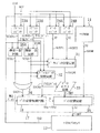
(第1の実施形態)
図1は本発明の第1の実施形態に係る記憶データ修正回路の構成図である。この回路はLSIに内蔵されており、いわゆる1チップマイコンの一部分を構成している。
【0027】
図1において、マイクロプロセッサ12は32ビット構成のプロセッサであり、アドレス信号SADを出力してマスクROM11に対するアクセスを行う。記憶手段としてのマスクROM11にはマイクロプロセッサ12が実行するプログラムが格納されている。
【0028】
マスクROM11は4(=22 )バイト幅の出力を持ち、4バイト(32ビット)のデータを一括して読み出すように構成されている。すなわち、アドレス信号SADは4の倍数のアドレス(すなわち下位2ビットが「0」)を指定するものであり、マスクROM11は一回の読み出しアクセスにおいて、アドレス信号SADが指定する4の倍数のアドレスから始まる連続4バイトのデータをROMデータ信号SROMとして出力する。なお、マスクROM11は、マイクロプロセッサ12が実行するプログラム以外に、マイクロプロセッサ12が処理に用いるデータもその一部に格納する。
【0029】
マイクロプロセッサ12は、1個の命令を構成する命令コードのバイト数が命令種毎に異なる命令体系を有しており、これによって、効率的なプログラミングが可能になっている。しかしながら、各命令はマスクROM11の任意のアドレスに記憶されるので、1個の命令を構成する命令コードが、1回の読み出しアクセスによって読み出される範囲(アドレス信号SADが指定するアドレスから始まる4バイト)に収まらず、2回またはそれ以上の読み出しアクセスを必要とする範囲にわたって配置される場合がある。
【0030】
またここでは、マイクロプロセッサ12はリトルエンディアンのバイトアドレスを採用しているものとする。すなわち、マスクROM11から読み出された4バイトのデータは、アドレス信号SADが指定するアドレスのデータから順に、ワード内の第0バイト、第1バイト、第2バイト、第3バイトとして用いられる。
【0031】
アドレスレジスタ13は修正アドレスSCADを保持し、データレジスタ14は4バイト(32ビット)の修正データSCDTを保持する。アドレスレジスタ13およびデータレジスタ14には、シリアル書込クロック信号CLKおよびシリアル書込データ信号WDTがそれぞれ入力される。これらの信号CLK,WDTは、図1の修正回路を内蔵する1チップマイコンの外部端子から供給される。そして、シリアル書込データ信号WDTの値をシリアル書込クロック信号CLKに同期して変化させることによって、アドレスレジスタ13とデータレジスタ14に、修正アドレスSCADおよび修正データSCDTとして、1チップマイコンの外部から任意の値が設定可能になっている。
【0032】
マイクロプロセッサ12から出力されたアドレス信号SADはマスクROM11以外に、隣接一致回路15にも入力される。隣接一致回路15は、入力されたアドレス信号SADとアドレスレジスタ13に設定された修正アドレスSCADとの比較を行い、隣接一致信号SCOを出力する。
【0033】
隣接一致回路15は、修正アドレスSCADが、アドレス信号SADが示すアドレスの,以降の4個のアドレスおよび手前の4個のアドレスに含まれるとき、隣接一致信号SCOとして“H”を出力する。すなわち、アドレス信号SADが、修正アドレスSCADを含む4バイトアラインから始まる4バイトとこれに続く4バイトへのアクセスを指したとき、隣接一致信号SCOとして“H”を出力する。具体的には、隣接一致回路15は、下位2ビットを除いたアドレス信号SADの値から下位2ビットを除いた修正アドレスSCADの値を減算し、減算結果が「0」または「1」のとき(これは(アドレス信号SAD−修正アドレスSCAD)の演算結果が「−3」以上「4」以下である場合に相当する)、隣接一致信号SCOとして“H”を出力する。
【0034】
隣接一致信号SCOは、バイト切替制御回路18に入力され、バイト切替回路19の制御に用いられる。バイト切替制御回路18およびバイト切替回路19によって、記憶データ選択部17が構成されている。
【0035】
図2は記憶データ選択部17の構成の詳細を示す図である。図2に示すように、バイト切替回路19は、4バイト幅のROMデータ信号SROMとデータレジスタ14から出力された4バイト幅の修正データSCDTとを入力とする。そして、ROMデータ信号SROMおよび修正データSCDTの各バイトに対応して設けられた4個の切替回路19a〜19dによって、バイト単位で、ROMデータ信号SROMおよび修正データSCDTのいずれかを選択し、データ信号SDTとして出力する。出力されたデータ信号SDTは修正済記憶データとしてマイクロプロセッサ12に送られる。
【0036】
各切替回路19a〜19dの選択動作は、バイト切替制御回路18が出力する4個のバイト切替制御信号SSa〜SSdによって、それぞれ制御される。各切替回路19a〜19bは、バイト切替制御信号SSa〜SSdが“H”のときは修正データSCDTを選択し、そうでないときはROMデータ信号SROMを選択する。
【0037】
バイト切替制御回路18は隣接一致信号SCOに加えて、修正アドレスSCADの下位3(=2+1)ビットおよびアドレス信号SADの第2ビットを入力とし、バイト切替制御信号SSa〜SSdを生成する。バイト切替制御回路18は、隣接一致信号SCOが“H”であり、かつ、以下の条件が成立したとき、切替回路19a〜19dが修正データSCDTを選択するように、バイト切替制御信号SSa〜SSdとして“H”を出力する。
【0038】
・バイト切替制御信号SSa
修正アドレスSCADの第2ビットの値がアドレス信号SADの第2ビットの値と等しいとき
・バイト切替制御信号SSb
修正アドレスSCADの第2ビットの値がアドレス信号SADの第2ビットの値と等しく、かつ、修正アドレスSCADの下位2ビットの値が「3」未満、または、
修正アドレスSCADの第2ビットの値がアドレス信号SADの第2ビットの値と異なり、かつ、修正アドレスSCADの下位2ビットの値が「3」以上のとき
・バイト切替制御信号SSc
修正アドレスSCADの第2ビットの値がアドレス信号SADの第2ビットの値と等しく、かつ、修正アドレスSCADの下位2ビットの値が「2」未満、または、
修正アドレスSCADの第2ビットの値がアドレス信号SADの第2ビットの値と異なり、かつ、修正アドレスSCADの下位2ビットの値が「2」以上のとき
・バイト切替制御信号SSd
修正アドレスSCADの第2ビットの値がアドレス信号SADの第2ビットの値と等しく、かつ、修正アドレスSCADの下位2ビットの値が「1」未満、または、
修正アドレスSCADの第2ビットの値がアドレス信号SADの第2ビットの値と異なり、かつ、修正アドレスSCADの下位2ビットの値が「1」以上
以上のように構成された記憶データ修正回路について、以下、その動作を説明する。
【0039】
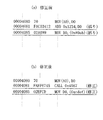
図3(a)は1チップマイコンの製造時にマスクROM11に記憶されたプログラムのリストの一部であって、修正前のものである。ここでは(後述する他のプログラムリストも同様)、最右欄に命令のニーモニックが、中央欄にその命令の命令コード(16進数表記)が、そして最左欄にその命令が記憶されているアドレス(16進数表記)が示されている。図3(a)のプログラムリストでは3個の命令が記載されており、4080番地にはメモリに記憶したデータをレジスタに読み込む命令(MOV)が、4081番地には読み出したデータを用いて加算を行う命令(ADD)が、そして4085番地には加算結果をメモリに記録する命令(MOV)が、それぞれ配置されている。これらの命令の命令コードのサイズはそれぞれ、1バイト、4バイトおよび3バイトである。ここで、2番目のADD命令の命令コードは、2回の読み出しアクセスを必要とする範囲(4080番地から始まる4バイトと4084番地から始まる4バイト)にわたって配置されている。
【0040】
図3(a)に示すプログラムが修正なしでそのまま用いられる場合には、マスクROM11から4バイト単位で出力されるROMデータ信号SROMは、そのままマイクロプロセッサ12に送られる。
【0041】
まず、4080番地から始まる4バイト(順に「70」「FA」「C0」「34」)がROMデータ信号SROMとして出力される。このとき、アドレスレジスタ13には修正アドレスSCADが設定されていないので、隣接一致回路15が隣接一致信号SCOとして“H”を出力することはなく、バイト切替制御回路18から出力されるバイト切替制御信号SSa〜SSdはいずれも“L”のままである。したがって、バイト切替回路19はROMデータ信号SROMとして入力される4バイトのデータをそのままデータ信号SDTとして出力する。この結果、マスクROM11に記憶された4080番地から始まる4バイトのデータがそのままマイクロプロセッサ12に送られる。同様に、4084番地から始まる4バイト(順に「12」「02」「AB」「89」)が、そのままデータ信号SDTとしてマイクロプロセッサ12に送られる。
【0042】
ここで、マスクROM11にプログラムが書き込まれ、1チップマイコンとして製造された後に、4081番地のADD命令に誤りが発見されたものとする。このとき、図3(b)に示すように、4081番地のADD命令をサブルーチン分岐命令(CALL)に置き換えることによって、このプログラムの誤りを修正するものとする。
【0043】
この修正を行うために、マイクロプロセッサ12がプログラムを実行する以前例えばリセット期間中に、1チップマイコンの外部端子からシリアル書込クロック信号CLKとシリアル書込データ信号WDTによって、アドレスレジスタ13に修正アドレスSCADとして4081番地を設定するとともに、データレジスタ14に修正データSCDTとして命令コード(FA,FF,67,45)を設定する。
【0044】
なお、修正データSCDTの設定は、修正アドレスSCADの下位2ビットの値が示すバイト位置から順に行う必要がある。この例では、修正アドレスSCAD(4081番地)の下位2ビットの値は「1」であるので、修正データSCDTの先頭データ「FA」をデータレジスタ14の第1バイトに配置し、以降、データ「FF」「67」「45」をそれぞれ第2バイト、第3バイトおよび第0バイトに配置する。
【0045】
修正アドレスSCADおよび修正データSCDTが設定された後の動作について、説明する。
【0046】
マイクロプロセッサ12が4080番地をアクセスするとき、プログラム未修正時と同様に、マスクROM11からはROMデータ信号SROMとして、製造時に書き込まれたデータすなわち「70」「FA」「C0」「34」が出力される。このとき、隣接一致回路15は上述したような動作によって、アドレス信号SAD(4080番地)とアドレスレジスタ13から出力された修正アドレスSCAD(4081番地)とを比較し、隣接一致信号SCOとして“H”を出力する。
【0047】
バイト切替制御回路18は、アドレス信号SADの第2ビットが“0”であり、修正アドレスSCADの第2ビットが“0”、下位2ビットの値が「1」であることから、バイト切替制御信号SSa〜SScとして“H”を出力し、バイト切替制御信号SSdとして“L”を出力する。これにより、バイト切替回路19において、切替回路19a〜19cはデータレジスタ14から出力された修正データSCDTを選択する一方、切替回路19dは修正前と同様にROMデータ信号SROMを選択する。この結果、データ信号SDTとして、第0バイトに「70」、第1バイトに「FA」、第2バイトに「FF」、第3バイトに「67」が出力される。
【0048】
また、マイクロプロセッサ12が4084番地をアクセスするとき、プログラム未修正時と同様に、マスクROM11からはROMデータ信号SROMとして、製造時に書き込まれたデータすなわち「12」「02」「AB」「89」が出力される。この場合にも、隣接一致回路15はアドレス信号SAD(4084番地)と修正アドレスSCAD(4081番地)とを比較し、隣接一致信号SCOとして“H”を出力する。
【0049】
バイト切替制御回路18は、アドレス信号SADの第2ビットが“1”であるので、ここでは、バイト切替制御信号SSa〜SScとして“L”を出力し、バイト切替制御信号SSdとして“H”を出力する。これにより、バイト切替回路19において、切替回路19a〜19cはROMデータ信号SROMを選択する一方、切替回路19dは修正データSCDTを選択する。この結果、データ信号SDTとして、第0バイトに「45」、第1バイトに「02」、第2バイトに「AB」、第3バイトに「89」が出力される。
【0050】
一方、マイクロプロセッサ12が4080番地と4084番地以外をアクセスする場合は、隣接一致回路15は隣接一致信号SCOとして“L”を出力する。これにより、マスクROM11から出力されたROMデータ信号SROMが、そのままデータ信号SDTとしてマイクロプロセッサ12に送られる。
【0051】
このように、アドレスレジスタ13に修正アドレスSCADとして4081番地を設定し、データレジスタ14に修正データSCDTとして「45」「FA」「FF」「67」を設定することによって、4080番地に対するアクセスにおいては「70」「FA」「FF」「67」の4バイトが、4084番地に対するアクセスにおいては「45」「02」「AB」「89」の4バイトが、データ信号SDTとしてマイクロプロセッサ12に送られる。この結果、図3(b)に示すようなプログラムの修正が実現される。
【0052】
以上のように本実施形態によると、隣接一致回路15とバイト切替制御回路18の制御により、バイト切替回路19において、マスクROM11の出力SROMと修正データSCDTとをバイト単位で選択することによって、図3の例のように2回の読み出しアクセスを必要とする範囲にわたって配置された命令(命令コードが4バイト以下)を、容易に修正することができる。
【0053】
なお、本実施形態では、マイクロプロセッサ12はリトルエンディアンのバイトアドレスを採用しているものとしたが、ビッグエンディアンのバイトアドレスを採用したマイクロプロセッサを用いた場合でも、本発明は容易に適用可能である。この場合、バイト切替制御回路18が出力するバイト切替制御信号SSa〜SSdとバイト切替回路19の切替回路19a〜19dとの対応関係を変更し、各バイト切替制御信号SSa〜SSdが、切替回路19d〜19aをそれぞれ制御するようにすればよい。
【0054】
(第2の実施形態)
図4は本発明の第2の実施形態に係る記憶データ修正回路の構成図である。この回路もLSIに内蔵されており、いわゆる1チップマイコンの一部分を構成している。図4において、図1と共通の構成要素には、図1と同一の符号を付しており、ここではその詳細な説明を省略する。
【0055】
図4の構成では、アドレスレジスタおよびデータレジスタをそれぞれ2個ずつ設けており、これにより、マスクROM11に記憶されたデータの2箇所の誤りを修正可能になっている。
【0056】
第1および第2のアドレスレジスタ23A,23Bは修正アドレスSCAD1,SCAD2をそれぞれ保持し、第1および第2のデータレジスタ24A,24Bは4バイト(32ビット)の修正データSCDT1,SCDT2をそれぞれ保持する。アドレスレジスタ23A,23Bおよびデータレジスタ24A,24Bには、第1の実施形態と同様に、シリアル書込クロック信号CLKおよびシリアル書込データ信号WDTによって、1チップマイコンの外部から、修正アドレスSCAD1,SCAD2および修正データSCDT1,SCDT2として、任意の値が設定可能になっている。
【0057】
第1および第2の隣接一致回路25A,25Bはそれぞれ、入力されたアドレス信号SADと、第1および第2のアドレスレジスタ23A,23Bに設定された修正アドレスSCAD1,SCAD2との比較を行い、隣接一致信号SCO1,SCO2を出力する。隣接一致回路25Aおよび25Bは、各修正アドレスSCAD1,SCAD2が、アドレス信号SADが示すアドレスの,以降の4個のアドレスおよび手前の3個のアドレスに含まれるとき、隣接一致信号SCO1,SCO2として“H”を出力する。
【0058】
すなわち、修正アドレスSCAD1,SCAD2の下位2ビットが“0”でない場合は、アドレス信号SADが、修正アドレスSCAD1,SCAD2を含む4バイトアラインから始まる4バイトとこれに続く4バイトへのアクセスを指したとき、隣接一致信号SCO1,SCO2として“H”を出力する。ところが、修正アドレスSCAD1,SCAD2の下位2ビットが“0”の場合は、アドレス信号SADが修正アドレスSCAD1,SCAD2と一致したときにのみ、隣接一致信号SCO1,SCO2として“H”を出力する。この点で、本実施形態に係る隣接一致回路25A,25Bは、第1の実施形態に係る隣接一致回路15とは、その動作が異なる。
【0059】
具体的には、隣接一致回路25A,25Bは、下位2ビットを除いたアドレス信号SADの値から下位2ビットを除いた修正アドレスSCAD1,SCAD2の値を減算し、減算結果が「0」のとき、または、減算結果が「1」でありかつ修正アドレスSCAD1,SCAD2の下位2ビットが「0」でないとき(これは(アドレス信号SAD−修正アドレスSCAD1,SCAD2)の演算結果が「−3」以上「3」以下である場合に相当する)、隣接一致信号SCO1,SCO2として“H”を出力する。
【0060】
隣接一致信号SCO1,SCO2は、データレジスタ切替回路31およびアドレスレジスタ切替回路32にそれぞれ入力される。
【0061】
データレジスタ切替回路31は、データレジスタ24A,24Bから出力された修正データSCDT1,SCDT2から、隣接一致信号SCO1,SCO2として“H”が出力された方の値を選択し、選択修正データSSCDTとして出力する。また、アドレスレジスタ切替回路32は、アドレスレジスタ23A,23Bから出力された修正アドレスSCAD1,SCAD2の下位3ビットから、隣接一致信号SCO1,SCO2として“H”が出力された方の値を選択し、選択修正アドレス信号SSCADとして出力する。
【0062】
データレジスタ切替回路31から出力された選択修正データSSCDTと、アドレスレジスタ切替回路32から出力された選択修正アドレス信号SSCADのうちの下位2ビットは、データローテート回路33に入力される。データローテート回路33は、選択修正データSSCDTが示す値を、選択修正アドレスSSCADの下位2ビットが示すバイト数分だけローテートさせ、ローテートデータSRTとして出力する。
【0063】
記憶データ選択部17は、第1の実施形態と同様の構成からなる。バイト切替制御回路18は、隣接一致信号SCO1,SCO2の論理和SSCOと選択修正アドレスSSCADとを入力し、第1の実施形態と同様の論理によって、4個のバイト切替制御信号SSa〜SSdを生成する。また、バイト切替回路19は、4バイト幅のROMデータ信号SROMとデータローテート回路33から出力されたローテートデータSRTとを入力とする。そして、バイト切替制御信号SSa〜SSdの制御によって、バイト単位で、ROMデータ信号SROMとローテートデータSRTのいずれかを選択し、データ信号SDTとして出力する。出力されたデータ信号SDTはマイクロプロセッサ12に送られる。
【0064】
以上のように構成された記憶データ修正回路について、以下、その動作を説明する。
【0065】
図5(a)は1チップマイコンの製造時にマスクROM11に記憶されたプログラムのリストの一部であって、修正前のものである。ここでは、4081番地のADD命令に加えて、4105番地のAND命令および4109番地のCMP命令にも、製造後に誤りが発見されたものとしている。したがって、図5(b)に示す修正後のプログラムリストでは、4081番地のADD命令をCALL命令(「FA」「FF」「67」「45」)に置き換え、さらに、4107番地からの4バイトを「08」「00」「A0」「08」に置き換えることによって、上述の誤りを修正している。
【0066】
この修正を行うために、マイクロプロセッサ12がプログラムを実行する以前例えばリセット期間中に、1チップマイコンの外部端子からシリアル書込クロック信号CLKとシリアル書込データ信号WDTによって、アドレスレジスタ23A,23Bに修正アドレスSCAD1,SCAD2として4081番地、4107番地を設定するとともに、データレジスタ24A,24Bに修正データSCDT1,SCDT2として「FA」「FF」「67」「45」および「08」「00」「A0」「08」をそれぞれ設定する。
【0067】
なお、本実施形態では、第1の実施形態のように、修正データSCDT1,SCDT2の配置を修正アドレスSCAD1,SCAD2の下位2ビットの値に従って定める必要はない。すなわち、修正データSCDT1,SCDT2は、データレジスタ24A,24Bの第0バイトから順に配置すればよい。これは、データローテート回路33を設けたことによって得られた効果であり、データローテート回路33の具体的な動作については、後述する。
【0068】
修正アドレスSCAD1,SCAD2および修正データSCDT1,SCDT2が設定された後の動作について、説明する。
【0069】
マイクロプロセッサ12が4080番地をアクセスするとき、マスクROM11からはROMデータ信号SROMとして、製造時に書き込まれたデータすなわち「70」「FA」「C0」「34」が出力される。このとき、第1の隣接一致回路25Aはアドレス信号SAD(4080番地)と第1のアドレスレジスタ23Aから出力された修正アドレスSCAD1(4081番地)とを比較し、隣接一致信号SCO1として“H”を出力する。一方、第2の隣接一致回路25Bはアドレス信号SAD(4080番地)と第2のアドレスレジスタ23Bから出力された修正アドレスSCAD2(4107番地)とを比較し、隣接一致信号SCO2として“L”を出力する。
【0070】
アドレスレジスタ切替回路32は、第1の隣接一致信号SCO1が“H”であるので、第1のアドレスレジスタ23Aから出力された修正アドレスSCAD1(4081番地)の下位3ビットを選択し、選択修正アドレスSSCADとして出力する。また、データレジスタ切替回路31も、第1の隣接一致信号SCO1が“H”であるので、第1のデータレジスタ24Aから出力された修正データSCDT1を選択し、選択修正データSSCDTとして出力する。
【0071】
このとき、データローテート回路33に入力される選択修正アドレスSSCADの下位2ビットは、「1」になる。このため、データローテート回路33は、選択修正データSSCDTとして入力されるデータレジスタ24Aの出力「FA」「FF」「67」「45」を1バイト分だけローテートし、ローテートデータ信号SRTとして「45」「FA」「FF」「67」を出力する。
【0072】
バイト切替制御回路18は、アドレス信号SADの第2ビットが“0”であり、選択修正アドレスSSCADの第2ビットが“0”、下位2ビットの値が「1」であることから、バイト切替制御信号SSa〜SScとして“H”を出力し、バイト切替制御信号SSdとして“L”を出力する。これにより、バイト切替回路19は、データ信号SDTとして、第0バイトはROMデータ信号SROMを選択し、第1〜3バイトはローテートデータ信号SRTを選択する。この結果、データ信号SDTとして「70」「FA」「FF」「67」が出力される。
【0073】
また、マイクロプロセッサ12が4084番地をアクセスするときも同様に、隣接一致回路25Aは隣接一致信号SCO1として“H”を出力し、隣接一致回路25Bは隣接一致信号SCO2として“L”を出力する。この結果、データ信号SDTとして「45」「02」「AB」「89」が出力される。
【0074】
マイクロプロセッサ12が4104番地をアクセスするとき、隣接一致回路25Aはアドレス信号SAD(4104番地)と修正アドレスSCAD1(4081番地)とを比較し、隣接一致信号SCO1としてL”を出力する一方、隣接一致回路25Bはアドレス信号SAD(4104番地)と修正アドレスSCAD2(4107番地)とを比較し、隣接一致信号SCO2として“H”を出力する。したがって、アドレスレジスタ切替回路32は修正アドレスSCAD2(4107番地)の下位3ビットを選択し、選択修正アドレスSSCADとして出力する。また、データレジスタ切替回路31も修正データSCDT2を選択し、選択修正データSSCDTとして出力する。
【0075】
このとき、データローテート回路33に入力される選択修正アドレスSSCADの下位2ビットは、「3」になる。このため、データローテート回路33は、選択修正データSSCDTとして入力されるデータレジスタ24Bの出力「08」「00」「A0」「08」を3バイト分ローテートし、ローテートデータ信号SRTとして「00」「A0」「08」「08」を出力する。
【0076】
バイト切替制御回路18は、アドレス信号SADの第2ビットが“1”であり、選択修正アドレスSSCADの第2ビットが“1”、下位2ビットの値が「3」であることから、バイト切替制御信号SSa〜SScとして“L”を出力し、バイト切替制御信号SSdとして“H”を出力する。これにより、バイト切替回路19はデータ信号SDTとして「71」「FA」「E0」「08」を出力する。
【0077】
また、マイクロプロセッサ12が4108番地をアクセスするときも同様に、隣接一致回路25Aは隣接一致信号SCO1として“L”を出力し、隣接一致回路25Bは隣接一致信号SCO2として“H”を出力する。この結果、データ信号SDTとして「00」「A0」「08」「C8」が出力される。
【0078】
一方、マイクロプロセッサ12が4080番地、4084番地、4104番地および4108番地以外をアクセスする場合は、隣接一致回路25A,25Bは隣接一致信号SCO1,SCO2として“L”を出力する。これにより、マスクROM11から出力されたROMデータ信号SROMが、そのままデータ信号SDTとしてマイクロプロセッサ12に送られる。
【0079】
このように、アドレスレジスタ23A,23Bに修正アドレスSCAD1,SCAD2として4081番地および4107番地を設定し、データレジスタ24A,24Bに修正データSCDT1,SCDT2として「FA」「FF」「67」「45」および「08」「00」「A0」「08」を設定することによって、各修正アドレスSCAD1,SCAD2に対してアクセスした場合には修正データSCDT1,SCDT2がマイクロプロセッサ12に送られる。この結果、図5(b)に示すようなプログラムの修正が実現される。
【0080】
図6(a)も1チップマイコンの製造時にマスクROM11に記憶されたプログラムのリストの一部であって、修正前のものである。ここでは、4081番地のADD命令に加えて、4085番地のMOV命令にも誤りが発見されたものとしている。したがって、図6(b)に示す修正後のプログラムリストでは、4081番地から4バイトを「FA」「FF」「67」「45」に置き換え、さらに4085番地からの3バイトを「02」「EF」「CD」に置き換えることによって、上述の誤りを修正している。
【0081】
このように連続4バイトを越えて修正を行う場合には、本実施形態では、アドレスレジスタ23A,23Bに修正アドレスSCAD1,SCAD2として4バイトアラインのアドレスを設定する。すなわち、アドレスレジスタ23A,23Bに修正アドレスSCAD1,SCAD2として4080番地、4084番地を設定するとともに、データレジスタ24A,24Bに修正データSCDT1,SCDT2として「70」「FA」「FF」「67」および「45」「02」「EF」「CD」をそれぞれ設定する。
【0082】
このように設定を行った後、マイクロプロセッサ12が4080番地をアクセスするときは、第1の隣接一致信号SCO1として“H”が出力され、第2の隣接一致信号SCO2として“L”が出力される。このとき、データレジスタ24Aから出力された修正データSCDT1が、データレジスタ切替回路31から選択修正データSSCDTとして出力され、さらにデータローテート回路33からローテートデータ信号SRTとして出力される。また、バイト切替制御信号SSa〜SSdとして全て“H”が出力されるので、データ信号SDTとしては、データレジスタ24Aから出力された修正データSCDT1の値すなわち「70」「FA」「FF」「67」が出力される。
【0083】
また、マイクロプロセッサ12が4084番地をアクセスするときは、第1の隣接一致信号SCO1として“L”が出力され、第2の隣接一致信号SCO2として“H”が出力される。したがって、データ信号SDTとしては、データレジスタ24Bから出力された修正データSCDT2の値すなわち「45」「02」「EF」「CD」が出力される。この結果、図6(b)に示すようなプログラムの修正が実現される。
【0084】
以上のように本実施形態によると、アドレスレジスタ、データレジスタおよび隣接一致回路を2個ずつ設けることによって、図5の例のように、2回の読み出しアクセスを必要とする2箇所の修正を行うことが可能になる。また、各隣接一致回路は、修正アドレスが4バイトアラインにあるとき、隣接するアドレスに対するアクセスを判断しないので、4バイト境界のアドレスから始まる4バイト以上のデータを連続して修正することが可能となる。
【0085】
また、修正データを修正アドレスの下位2ビットの値に相当するバイト数分ローテートするデータローテート回路を設けたことによって、修正データを、修正を行う並び順のままデータレジスタに設定することが可能になる。もちろん、データローテート回路を設けないで、データレジスタ切替回路31から出力された選択修正データSSCDTをそのままバイト切替回路19に入力させるように構成してもかまわない。ただしこの場合は、第1の実施形態と同様に、修正データの設定を、修正アドレスの下位2ビットの値が示すバイト位置から順に行う必要がある。
【0086】
一方、本実施形態に係るデータローテート回路を、第1の実施形態に係る構成に設けることによって、本実施形態と同様の効果を得ることができる。すなわち、図1の構成において、データレジスタ14とバイト切替回路19との間に、修正データSCDTを修正アドレスSCADの下位2ビットの値に相当するバイト数分ローテートするデータローテート回路を設けることによって、修正データSCDTを、修正を行う並び順のままデータレジスタ14に設定することが可能になる。
【0087】
なお、本実施形態では、アドレスレジスタとデータレジスタ、および隣接一致回路をそれぞれ2組ずつ設けるものとしたが、これらをそれぞれ3組以上設けてもかまわないことは明らかである。
【0088】
また、上述した各実施形態では、N=2とし、マスクROM11は4(=22 )バイトを一括して読み出す構成であるものとしたがが、一般に、2のべき乗に相当する数のバイト幅の出力を持つマスクROMを用いた場合に、本発明は同様に適用可能であることは明らかである。
【0089】
また、上述した各実施形態では、修正アドレスおよび修正データは、1チップマイコンの外部端子から設定されるものとしたが、この代わりに、マイクロプロセッサ12が実行するプログラムによって設定する構成とすることも可能である。この場合、例えば、1チップマイコンの外部または内部に設けたFlash ROMなどの書き換え可能なメモリ素子に修正アドレスおよび修正データを格納しておき、ブートプログラムに、これらの値がアドレスレジスタおよびデータレジスタに設定されるように、プログラミングすればよい。
【0090】
また、上述した各実施形態では、マスクROM11に記憶された命令コードの修正を行っているが、命令コード以外のデータであっても、同様に修正を行うことは可能である。
【0091】
また、上述した各実施形態では、マスクROMに記録されたデータの修正を行うものとしたが、マスクROM以外の記憶手段に記録されたデータの修正も、同様に実現できることはいうまでもない。
【0092】
【発明の効果】
以上のように本発明によると、修正アドレスまたはこれに隣接したアドレスに対するアクセスを検出したとき、記憶手段の出力データおよび修正データのいずれかが、バイト単位で、アドレス信号および修正アドレスに応じて選択される。これによって、任意のアドレスからのデータ修正が可能になり、例えばアクセスの境界を跨ぐように記憶された命令コードの修正も可能になる。
【図面の簡単な説明】
【図1】 本発明の第1の実施形態に係る記憶データ修正回路の構成図である。
【図2】 図1の構成における記憶データ選択部の詳細な構成を示す図である。
【図3】 第1の実施形態における修正対象のプログラム例を示すリストである。
【図4】 本発明の第2の実施形態に係る記憶データ修正回路の構成図である。
【図5】 第2の実施形態における修正対象のプログラム例を示すリストである。
【図6】 第2の実施形態における修正対象のプログラム例を示すリストである。
【図7】 従来の記憶データ修正回路の構成図である。
【符号の説明】
11 マスクROM(記憶手段)
13 アドレスレジスタ
14 データレジスタ
15 隣接一致回路
17 記憶データ選択部
18 バイト切替制御回路
19 バイト切替回路
23A,23B アドレスレジスタ
24A,24B データレジスタ
25A,25B 隣接一致回路
31 データレジスタ切替回路
32 アドレスレジスタ切替回路
33 データローテート回路
SAD アドレス信号
SCAD 修正アドレス
SCDT 修正データ
SROM ROMデータ信号(記憶手段の出力データ)
SDT データ信号(修正済記憶データ)
SCAD1,SCAD2 修正アドレス
SCDT1,SCDT2 修正データ
SSCAD 選択修正アドレス
SSCDT 選択修正データ
SRT ローテートデータ(データローテート回路の出力)[0001]
BACKGROUND OF THE INVENTION
The present invention belongs to a circuit technique for correcting an error in data recorded in a storage means such as a mask ROM used in an LSI such as a microprocessor or a digital signal processor (DSP).
[0002]
[Prior art]
In recent years, digital LSIs such as microprocessors and DSPs have been increasingly integrated year by year, and are equipped with large-capacity memory circuits. In particular, a mask ROM can be integrated with a larger capacity than other memory elements, and is mainly used for storing a program executed by a processor.
[0003]
The mask ROM is a non-rewritable storage element, and programs and data executed by the processor are written in the LSI manufacturing stage. However, as the amount of the program increases, the possibility that the program includes an error increases, and it has become difficult to completely eliminate the program error in the LSI manufacturing stage. Therefore, when there is an error in the program or data recorded in the mask ROM at the LSI manufacturing stage, a function is required to correct the error when using the LSI.
[0004]
FIG. 7 is a block diagram showing an example of a conventional stored data correction circuit. In FIG. 7, a
[0005]
In the configuration of FIG. 7, when an error is found in the program or data recorded in the
[0006]
[Problems to be solved by the invention]
In the conventional configuration described above, when the microprocessor accesses an erroneous address, the data read from the mask ROM is switched to the correction data set in the data register at once.
[0007]
However, in this configuration, when a mask ROM having a configuration in which a plurality of bytes, for example, a 4-byte width is output and 4-byte data is read out at a time, error correction is also performed with a 4-byte alignment (a multiple of 4). 4 bytes of data starting from the address (1) are corrected in a batch. In this case, it becomes difficult to perform correction from an arbitrary address.
[0008]
In particular, when a microprocessor having a different instruction system for each instruction type is used as the instruction code constituting one instruction, the instruction code of one instruction in the program is 4 in the mask ROM. It may be arranged across byte-aligned addresses. With respect to such an instruction that crosses the access boundary, in the conventional configuration described above, it is difficult to correct even if the number of bytes of the instruction is 4 or less.
[0009]
In view of the above problems, an object of the present invention is to provide a storage data correction circuit capable of correcting data from an arbitrary address for a storage means such as a mask ROM having a multi-byte output.
[0010]
[Means for Solving the Problems]
In order to solve the above problems, a stored data correction circuit according to the present invention includes an adjacent match circuit that detects access to a corrected address or an address adjacent thereto, an output of a storage unit according to a value of a lower bit of the corrected address, And a storage data selection unit that controls switching with the correction data in units of bytes.
[0011]
Specifically, the solution provided by the invention of claim 1 is 2N(N is a natural number) 2 byte output, indicated by the
[0012]
According to the first aspect of the invention, the access to the corrected address or the address adjacent thereto can be detected by the adjacent coincidence circuit, and when detected, the output data and the corrected data of the storage means are detected by the storage data selection unit. Either one is selected in byte units according to the address signal and the modified address. As a result, it is possible to correct data from an arbitrary address, and it is also possible to correct the instruction code stored so as to cross the access boundary.
[0013]
In the invention of
[0014]
According to a third aspect of the present invention, the byte switching control circuit in the stored data correction circuit according to the second aspect is configured such that the Mth (M is 0 ≦ M <(2NAs an output of an integer) byte, an adjacent match is detected by the adjacent match circuit, and the value of the Nth bit of the address signal is equal to the value of the Nth bit of the modified address and the lower N of the modified address The value of the bit is less than (M + 1), or the value of the Nth bit of the address signal is different from the value of the Nth bit of the modified address, and the value of the lower N bits of the modified address is (M + 1) or more Is controlled such that the Mth byte of the correction data is selected, and otherwise, the Mth byte of the output of the storage means is selected. This control is effective when a little endian byte address is adopted.
[0015]
According to a fourth aspect of the present invention, the stored data correction circuit according to the first aspect is configured to store the correction data in byte units.,A data rotation circuit that rotates by the number of bytes corresponding to the value of the lower N bits of the correction address, and the storage data selection unit inputs the output of the data rotation circuit as a selection target instead of the correction data And
[0016]
According to the invention of
[0017]
According to a fifth aspect of the present invention, the adjacent match circuit in the stored data correction circuit of the first aspect subtracts the value of the corrected address excluding the lower N bits from the value of the address signal excluding the lower N bits. When “0” or “1” is set, an adjacent match is detected.
[0018]
Further, the solution provided by the invention of claim 6 is 2N(N is a natural number) 2 byte output, indicated by the
[0019]
According to a seventh aspect of the present invention, the storage data selection unit in the storage data correction circuit of the sixth aspect receives the output of the storage means and the selection correction data output from the data register switching circuit, and is in byte units. Byte switching circuit for selectively outputting one of them, the Nth bit of the address signal, the lower (N + 1) bits of the selected correction address output from the address register switching circuit, and the outputs of the plurality of adjacent match circuits And a byte switching control circuit for controlling the selection operation of the byte switching circuit.
[0020]
Furthermore, in the invention according to claim 8, the byte switching control circuit in the storage data correction circuit according to claim 7 is the Mth in the byte switching circuit (M is 0 ≦ M <(2NAs an output of an integer) byte, an adjacent match is detected by any of the plurality of adjacent match circuits, and the value of the Nth bit of the address signal is equal to the value of the Nth bit of the selected correction address; The value of the lower N bits of the selected corrected address is less than (M + 1), or the value of the Nth bit of the address signal is different from the value of the Nth bit of the selected corrected address and the lower N bits of the selected corrected address If the value is equal to or greater than (M + 1), the Mth byte of the correction data is selected, while if not, the Mth byte of the output of the storage means is selected. This control is effective when a little endian byte address is adopted.
[0021]
According to a ninth aspect of the present invention, the storage data correction circuit according to the sixth aspect further comprises a data rotation circuit for rotating the selection correction data by the number of bytes corresponding to the value of the lower N bits of the selection correction address in bytes. The stored data selection unit inputs the output of the data rotation circuit as a selection target instead of the selection correction data.
[0022]
According to the ninth aspect of the present invention, it becomes possible to set the correction data in the data register in the arrangement order in which correction is performed.
[0023]
According to a tenth aspect of the present invention, each of the plurality of adjacent match circuits in the stored data correction circuit according to the sixth aspect subtracts the value of the corrected address excluding the lower N bits from the value of the address signal excluding the lower N bits. When the subtraction result is “0”, or when the subtraction result is “1” and the value of the lower N bits of the correction address is not “0”, the adjacent match is detected.
[0024]
The solution provided by the invention of
[0025]
DETAILED DESCRIPTION OF THE INVENTION
Hereinafter, embodiments of the present invention will be described with reference to the drawings.
[0026]
(First embodiment)
FIG. 1 is a configuration diagram of a stored data correction circuit according to the first embodiment of the present invention. This circuit is built in the LSI and forms part of a so-called one-chip microcomputer.
[0027]
In FIG. 1, a
[0028]
The
[0029]
The
[0030]
Here, it is assumed that the
[0031]
The
[0032]
The address signal SAD output from the
[0033]
The
[0034]
The adjacent match signal SCO is input to the byte
[0035]
FIG. 2 is a diagram showing details of the configuration of the stored
[0036]
Each switching
[0037]
The byte
[0038]
・ Byte switching control signal SSa
When the value of the second bit of the modified address SCAD is equal to the value of the second bit of the address signal SAD
・ Byte switching control signal SSb
The value of the second bit of the modified address SCAD is equal to the value of the second bit of the address signal SAD and the value of the lower 2 bits of the modified address SCAD is less than “3”, or
When the value of the second bit of the modified address SCAD is different from the value of the second bit of the address signal SAD and the value of the lower 2 bits of the modified address SCAD is “3” or more
・ Byte switching control signal SSc
The value of the second bit of the modified address SCAD is equal to the value of the second bit of the address signal SAD and the value of the lower 2 bits of the modified address SCAD is less than “2”, or
When the value of the second bit of the modified address SCAD is different from the value of the second bit of the address signal SAD, and the value of the lower 2 bits of the modified address SCAD is “2” or more
・ Byte switching control signal SSd
The value of the second bit of the modified address SCAD is equal to the value of the second bit of the address signal SAD and the value of the lower 2 bits of the modified address SCAD is less than “1”, or
The value of the second bit of the modified address SCAD is different from the value of the second bit of the address signal SAD, and the value of the lower 2 bits of the modified address SCAD is “1” or more.
The operation of the stored data correction circuit configured as described above will be described below.
[0039]
FIG. 3A is a part of a list of programs stored in the
[0040]
When the program shown in FIG. 3A is used without modification, the ROM data signal SROM output from the
[0041]
First, 4 bytes starting from address 4080 (in order “70”, “FA”, “C0”, “34”) are output as the ROM data signal SROM. At this time, since the corrected address SCAD is not set in the
[0042]
Here, it is assumed that an error is found in the ADD instruction at address 4081 after the program is written in the
[0043]
In order to perform this correction, before the
[0044]
The correction data SCDT needs to be set in order from the byte position indicated by the lower 2 bits of the correction address SCAD. In this example, since the value of the lower 2 bits of the modified address SCAD (address 4081) is “1”, the first data “FA” of the modified data SCDT is arranged in the first byte of the data register 14 and thereafter the data “ “FF”, “67”, and “45” are arranged in the second byte, the third byte, and the zeroth byte, respectively.
[0045]
An operation after the correction address SCAD and the correction data SCDT are set will be described.
[0046]
When the
[0047]
Since the second bit of the address signal SAD is “0”, the second bit of the modified address SCAD is “0”, and the value of the lower 2 bits is “1”, the byte
[0048]
When the
[0049]
Since the second bit of the address signal SAD is “1”, the byte
[0050]
On the other hand, when the
[0051]
In this way, by setting address 4081 as the modified address SCAD in the
[0052]
As described above, according to the present embodiment, under the control of the
[0053]
In the present embodiment, the
[0054]
(Second Embodiment)
FIG. 4 is a configuration diagram of a stored data correction circuit according to the second embodiment of the present invention. This circuit is also built in the LSI and forms part of a so-called one-chip microcomputer. In FIG. 4, the same components as those in FIG. 1 are denoted by the same reference numerals as those in FIG. 1, and detailed description thereof is omitted here.
[0055]
In the configuration of FIG. 4, two address registers and two data registers are provided, so that two errors in the data stored in the
[0056]
The first and second address registers 23A and 23B hold correction addresses SCAD1 and SCAD2, respectively, and the first and second data registers 24A and 24B hold 4-byte (32 bits) correction data SCDT1 and SCDT2, respectively. . Similarly to the first embodiment, the address registers 23A and 23B and the data registers 24A and 24B receive the corrected addresses SCAD1 and SCAD2 from the outside of the one-chip microcomputer by the serial write clock signal CLK and the serial write data signal WDT. Also, arbitrary values can be set as the correction data SCDT1 and SCDT2.
[0057]
The first and second
[0058]
That is, when the lower 2 bits of the modified addresses SCAD1 and SCAD2 are not “0”, the address signal SAD indicates access to the 4 bytes starting from the 4-byte alignment including the modified addresses SCAD1 and SCAD2, and the subsequent 4 bytes. At this time, “H” is output as the adjacent coincidence signals SCO1 and SCO2. However, when the lower two bits of the correction addresses SCAD1 and SCAD2 are “0”, “H” is output as the adjacent match signals SCO1 and SCO2 only when the address signal SAD matches the correction addresses SCAD1 and SCAD2. In this respect, the
[0059]
Specifically, the
[0060]
The adjacent match signals SCO1 and SCO2 are input to the data register switching
[0061]
The data register switching
[0062]
The lower two bits of the selection / correction data SSCDT output from the data register switching
[0063]
The stored
[0064]
The operation of the stored data correction circuit configured as described above will be described below.
[0065]
FIG. 5A is a part of a list of programs stored in the
[0066]
In order to perform this correction, before the
[0067]
In this embodiment, unlike the first embodiment, it is not necessary to determine the arrangement of the correction data SCDT1 and SCDT2 according to the value of the lower 2 bits of the correction addresses SCAD1 and SCAD2. That is, the correction data SCDT1 and SCDT2 may be arranged in order from the 0th byte of the data registers 24A and 24B. This is an effect obtained by providing the data rotation circuit 33, and a specific operation of the data rotation circuit 33 will be described later.
[0068]
The operation after the correction addresses SCAD1, SCAD2 and correction data SCDT1, SCDT2 are set will be described.
[0069]
When the
[0070]
Since the first adjacent match signal SCO1 is “H”, the address
[0071]
At this time, the lower 2 bits of the selected correction address SSCAD input to the data rotation circuit 33 is “1”. For this reason, the data rotation circuit33Rotates the outputs “FA”, “FF”, “67”, “45” of the data register 24A input as the selection correction data SSCDT by one byte, and “45”, “FA”, “FF”, “” as the rotate data signal SRT. 67 "is output.
[0072]
Since the second bit of the address signal SAD is “0”, the second bit of the selected correction address SSCAD is “0”, and the value of the lower 2 bits is “1”, the byte
[0073]
Similarly, when the
[0074]
When the
[0075]
At this time, the lower 2 bits of the selected correction address SSCAD input to the data rotation circuit 33 is “3”. For this reason, the data rotation circuit33Rotates the output “08” “00” “A0” “08” of the
[0076]
Since the second bit of the address signal SAD is “1”, the second bit of the selected correction address SSCAD is “1”, and the value of the lower 2 bits is “3”, the byte
[0077]
Similarly, when the
[0078]
On the other hand, when the
[0079]
As described above, the addresses 4081 and 4107 are set as the corrected addresses SCAD1 and SCAD2 in the address registers 23A and 23B, and “FA”, “FF” “67” “45” and the corrected data SCDT1 and SCDT2 are set in the data registers 24A and 24B. By setting “08”, “00”, “A0”, and “08”, the correction data SCDT1 and SCDT2 are sent to the
[0080]
FIG. 6A is also a part of a list of programs stored in the
[0081]
In the case where correction is performed over four consecutive bytes as described above, in this embodiment, 4-byte aligned addresses are set as the correction addresses SCAD1 and SCAD2 in the address registers 23A and 23B. That is, addresses 4080 and 4084 are set as the corrected addresses SCAD1 and SCAD2 in the address registers 23A and 23B, and “70” “FA” “FF” “67” and “67” are set as the corrected data SCDT1 and SCDT2 in the data registers 24A and 24B. 45, “02”, “EF”, and “CD” are set.
[0082]
After the setting is made, when the
[0083]
When the
[0084]
As described above, according to the present embodiment, by providing two address registers, data registers, and adjacent coincidence circuits, two locations requiring two read accesses are corrected as in the example of FIG. It becomes possible. Further, each adjacent match circuit does not determine access to an adjacent address when the correction address is in a 4-byte alignment, so that it is possible to continuously correct data of 4 bytes or more starting from an address on a 4-byte boundary. Become.
[0085]
In addition, by providing a data rotation circuit that rotates the correction data by the number of bytes corresponding to the value of the lower 2 bits of the correction address, the correction data can be set in the data register in the order in which corrections are made. Become. Of course, the data rotation circuit may not be provided, and the selection correction data SSCDT output from the data register switching
[0086]
On the other hand, by providing the data rotation circuit according to the present embodiment in the configuration according to the first embodiment, the same effects as those of the present embodiment can be obtained. That is, in the configuration of FIG. 1, by providing a data rotation circuit that rotates the correction data SCDT by the number of bytes corresponding to the value of the lower 2 bits of the correction address SCAD between the data register 14 and the
[0087]
In this embodiment, two sets of address registers, data registers, and adjacent matching circuits are provided. However, it is obvious that three or more sets of these may be provided.
[0088]
In each of the embodiments described above, N = 2 and the
[0089]
In each of the above-described embodiments, the correction address and the correction data are set from the external terminal of the one-chip microcomputer. However, instead of this, the correction address and the correction data may be set by a program executed by the
[0090]
Further, in each of the above-described embodiments, the instruction code stored in the
[0091]
Further, in each of the above-described embodiments, the data recorded in the mask ROM is corrected, but it goes without saying that the correction of the data recorded in the storage means other than the mask ROM can be similarly realized.
[0092]
【The invention's effect】
As described above, according to the present invention, when access to a modified address or an address adjacent thereto is detected, either the output data or modified data of the storage means is selected in units of bytes according to the address signal and the modified address. Is done. As a result, it is possible to correct data from an arbitrary address. For example, it is possible to correct an instruction code stored so as to cross an access boundary.
[Brief description of the drawings]
FIG. 1 is a configuration diagram of a stored data correction circuit according to a first embodiment of the present invention.
FIG. 2 is a diagram showing a detailed configuration of a stored data selection unit in the configuration of FIG.
FIG. 3 is a list showing an example of a program to be modified in the first embodiment.
FIG. 4 is a configuration diagram of a stored data correction circuit according to a second embodiment of the present invention.
FIG. 5 is a list showing an example of a program to be modified in the second embodiment.
FIG. 6 is a list showing an example of a program to be modified in the second embodiment.
FIG. 7 is a configuration diagram of a conventional stored data correction circuit.
[Explanation of symbols]
11 Mask ROM (memory means)
13 Address register
14 Data register
15 Adjacent match circuit
17 Stored data selection section
18 byte switching control circuit
19 byte switching circuit
23A, 23B Address register
24A, 24B data register
25A, 25B Adjacent match circuit
31 Data register switching circuit
32 Address register switching circuit
33 Data rotation circuit
SAD address signal
SCAD correction address
SCDT correction data
SROM ROM data signal (output data of storage means)
SDT data signal (corrected stored data)
SCAD1, SCAD2 modified address
SCDT1, SCDT2 correction data
SSCAD selection correction address
SSCDT selection correction data
SRT rotate data (output of data rotation circuit)
Claims (11)
2N バイト幅の修正データを保持するデータレジスタと、
修正アドレスを保持するアドレスレジスタと、
前記アドレス信号および前記修正アドレスを入力とし、前記修正アドレスが、前記アドレス信号が示すアドレスの,以降の2N 個および手前の2N 個のアドレスのうちのいずれかに該当するとき、隣接一致を検出する隣接一致回路と、
前記隣接一致回路が隣接一致を検出したとき、前記記憶手段の出力データおよび前記修正データのいずれかを、バイト単位で、前記アドレス信号および前記修正アドレスに応じて、選択出力する記憶データ選択部とを備え、
前記記憶データ選択部の出力を、修正済記憶データとして出力する
ことを特徴とする記憶データ修正回路。Storage data for correcting output data for storage means having an output of 2 N (N is a natural number) byte width and reading out and outputting 2 N bytes of data stored from an address that is a multiple of 2 N indicated by the address signal A correction circuit,
A data register that holds 2 N byte wide correction data;
An address register that holds the modified address;
When the address signal and the modified address are input, and the modified address corresponds to any of the following 2 N addresses and the previous 2 N addresses of the address indicated by the address signal, an adjacent match is determined. An adjacent matching circuit to be detected;
A storage data selection unit that selectively outputs, in byte units, either the output data of the storage means or the correction data according to the address signal and the correction address when the adjacent match circuit detects an adjacent match; With
A storage data correction circuit, wherein the output of the storage data selection unit is output as corrected storage data.
前記記憶データ選択部は、
前記記憶手段の出力データおよび前記修正データを入力とし、バイト単位で、そのいずれかを、選択出力するバイト切替回路と、
前記アドレス信号の第Nビット、前記修正アドレスの下位(N+1)ビット、および前記隣接一致回路の出力を入力とし、前記バイト切替回路の選択動作の制御を行うバイト切替制御回路とを備えたものである
ことを特徴とする記憶データ修正回路。The stored data correction circuit according to claim 1.
The stored data selection unit
A byte switching circuit that receives the output data of the storage means and the correction data as input, and selectively outputs one of them in byte units,
A byte switching control circuit that receives the Nth bit of the address signal, the lower (N + 1) bits of the correction address, and the output of the adjacent match circuit and controls the selection operation of the byte switching circuit; A stored data correction circuit comprising:
前記バイト切替制御回路は、
前記バイト切替回路における第M(Mは0≦M<(2N )の整数)バイトの出力として、
前記隣接一致回路によって隣接一致が検出され、かつ、前記アドレス信号の第Nビットの値と前記修正アドレスの第Nビットの値が等しくかつ前記修正アドレスの下位Nビットの値が(M+1)未満、または、前記アドレス信号の第Nビットの値と前記修正アドレスの第Nビットの値が異なりかつ前記修正アドレスの下位Nビットの値が(M+1)以上である場合は、前記修正データの第Mバイトが選択される一方、
そうでない場合は、前記記憶手段の出力の第Mバイトが選択されるように、制御するものである
ことを特徴とする記憶データ修正回路。The stored data correction circuit according to claim 2,
The byte switching control circuit
As an output of the Mth byte (M is an integer of 0 ≦ M <(2 N )) in the byte switching circuit,
An adjacent match is detected by the adjacent match circuit, the value of the Nth bit of the address signal is equal to the value of the Nth bit of the modified address, and the value of the lower N bits of the modified address is less than (M + 1), Alternatively, if the value of the Nth bit of the address signal is different from the value of the Nth bit of the modified address and the value of the lower N bits of the modified address is equal to or greater than (M + 1), the Mth byte of the modified data While is selected
Otherwise, the stored data correction circuit is controlled so that the Mth byte of the output of the storage means is selected.
前記修正データを、バイト単位で、前記修正アドレスの下位Nビットの値に相当するバイト数分ローテートするデータローテート回路を備え、
前記記憶データ選択部は、
前記修正データの代わりに、前記データローテート回路の出力を、選択対象として入力するものである
ことを特徴とする記憶データ修正回路。The stored data correction circuit according to claim 1.
Wherein the correction data, in bytes, a data rotation circuit for rotating number of bytes corresponding to the value of the lower N bits of the modified address,
The stored data selection unit
A stored data correction circuit, wherein the output of the data rotation circuit is input as a selection target instead of the correction data.
前記隣接一致回路は、
下位Nビットを除く前記アドレス信号の値から下位Nビットを除く前記修正アドレスの値を減算した結果が「0」または「1」のとき、隣接一致を検出するものである
ことを特徴とする記憶データ修正回路。The stored data correction circuit according to claim 1.
The adjacent match circuit includes:
A memory that detects adjacent match when the result of subtracting the value of the modified address excluding the lower N bits from the value of the address signal excluding the lower N bits is “0” or “1”. Data correction circuit.
2N バイト幅の修正データをそれぞれ保持する複数のデータレジスタと、
前記各データレジスタに対応して設けられ、修正アドレスをそれぞれ保持する複数のアドレスレジスタと、
前記アドレスレジスタおよびデータレジスタの各組合わせに対応してそれぞれ設けられ、前記アドレス信号および対応する前記アドレスレジスタに保持された修正アドレスを入力とし、この修正アドレスが、前記アドレス信号が示すアドレスの,以降の2N 個および手前の(2N −1)個のアドレスのうちのいずれかに該当するとき、隣接一致を検出する複数の隣接一致回路と、
前記複数の隣接一致回路の出力を入力とし、隣接一致を検出した隣接一致回路に対応するデータレジスタに保持された修正データを、選択修正データとして出力するデータレジスタ切替回路と、
前記複数の隣接一致回路の出力を入力とし、隣接一致を検出した隣接一致回路に対応するアドレスレジスタに保持された修正アドレスを、選択修正アドレスとして出力するアドレスレジスタ切替回路と、
前記隣接一致回路が隣接一致を検出したとき、前記記憶手段の出力および前記データレジスタ切替回路から出力された選択修正データのいずれかを、バイト単位で、前記アドレス信号および前記アドレスレジスタ切替回路から出力された選択修正アドレスに応じて、選択出力する記憶データ選択部とを備え、
前記記憶データ選択部の出力を、修正済記憶データとして出力する
ことを特徴とする記憶データ修正回路。Storage data for correcting output data for storage means having an output of 2 N (N is a natural number) byte width and reading out and outputting 2 N bytes of data stored from an address that is a multiple of 2 N indicated by the address signal A correction circuit,
A plurality of data registers each holding 2 N bytes of modified data;
A plurality of address registers provided corresponding to each of the data registers, each holding a correction address;
Each of the address registers and the data registers is provided corresponding to each combination, and the address signal and the corrected address held in the corresponding address register are input, and the corrected address is an address indicated by the address signal, A plurality of adjacent match circuits that detect adjacent matches when corresponding to any of the subsequent 2 N addresses and (2 N -1) addresses before;
A data register switching circuit that outputs the correction data held in the data register corresponding to the adjacent coincidence circuit that has detected the adjacent coincidence as an input, the output of the plurality of adjacent coincidence circuits;
An address register switching circuit that outputs the correction address held in the address register corresponding to the adjacent coincidence circuit that has detected the adjacent coincidence, as an input, with the outputs of the plurality of adjacent coincidence circuits as inputs, and
When the adjacent match circuit detects an adjacent match, either the output of the storage means or the selection correction data output from the data register switching circuit is output from the address signal and the address register switching circuit in bytes. A storage data selection unit for selectively outputting according to the selected correction address ,
A storage data correction circuit, wherein the output of the storage data selection unit is output as corrected storage data.
前記記憶データ選択部は、
前記記憶手段の出力および前記データレジスタ切替回路から出力された選択修正データを入力とし、バイト単位で、そのいずれかを選択出力するバイト切替回路と、
前記アドレス信号の第Nビット、前記アドレスレジスタ切替回路から出力された選択修正アドレスの下位(N+1)ビット、および前記複数の隣接一致回路の出力を入力とし、前記バイト切替回路の選択動作の制御を行うバイト切替制御回路とを備えたものである
ことを特徴とする記憶データ修正回路。The stored data correction circuit according to claim 6.
The stored data selection unit
A byte switching circuit that receives the output of the storage means and the selection correction data output from the data register switching circuit as input, and selectively outputs one of them in byte units;
The Nth bit of the address signal, the lower (N + 1) bits of the selected correction address output from the address register switching circuit, and the outputs of the plurality of adjacent matching circuits are used as inputs to control the selection operation of the byte switching circuit. A stored data correction circuit comprising a byte switching control circuit for performing the operation.
前記バイト切替制御回路は、
前記バイト切替回路における第M(Mは0≦M<(2N )の整数)バイトの出力として、
前記複数の隣接一致回路のいずれかによって隣接一致が検出され、かつ、前記アドレス信号の第Nビットの値と前記選択修正アドレスの第Nビットの値が等しくかつ前記選択修正アドレスの下位Nビットの値が(M+1)未満、または、前記アドレス信号の第Nビットの値と前記選択修正アドレスの第Nビットの値が異なりかつ前記選択修正アドレスの下位Nビットの値が(M+1)以上である場合は、前記修正データの第Mバイトが選択される一方、
そうでない場合は、前記記憶手段の出力の第Mバイトが選択されるように、制御する
ことを特徴とする記憶データ修正回路。The stored data correction circuit according to claim 7,
The byte switching control circuit
As an output of the Mth byte (M is an integer of 0 ≦ M <(2 N )) in the byte switching circuit,
An adjacent match is detected by any of the plurality of adjacent match circuits, and the value of the Nth bit of the address signal is equal to the value of the Nth bit of the selected correction address and the lower N bits of the selected correction address When the value is less than (M + 1), or the value of the Nth bit of the address signal is different from the value of the Nth bit of the selected correction address, and the value of the lower N bits of the selected correction address is greater than or equal to (M + 1) While the Mth byte of the modified data is selected,
If not, the stored data correction circuit is controlled so that the Mth byte of the output of the storage means is selected.
前記選択修正データを、バイト単位で、前記選択修正アドレスの下位Nビットの値に相当するバイト数分ローテートするデータローテート回路を備え、
前記記憶データ選択部は、
前記選択修正データの代わりに、前記データローテート回路の出力を、選択対象として入力するものである
ことを特徴とする記憶データ修正回路。The stored data correction circuit according to claim 6.
A data rotation circuit for rotating the selection correction data by the number of bytes corresponding to the value of the lower N bits of the selection correction address in bytes;
The stored data selection unit
A stored data correction circuit, wherein the output of the data rotation circuit is input as a selection target instead of the selection correction data.
前記複数の隣接一致回路は、それぞれ、
下位Nビットを除く前記アドレス信号の値から下位Nビットを除く前記修正アドレスの値を減算し、この減算結果が「0」のとき、または減算結果が「1」でありかつ前記修正アドレスの下位Nビットの値が「0」でないとき、隣接一致を検出するものである
ことを特徴とする記憶データ修正回路。The stored data correction circuit according to claim 6.
Each of the plurality of adjacent coincidence circuits is
The value of the modified address excluding the lower N bits is subtracted from the value of the address signal excluding the lower N bits, and when the subtraction result is “0” or the subtraction result is “1” and the lower address of the modified address A stored data correction circuit for detecting adjacent match when the value of N bit is not "0".
Nバイト幅の修正データを保持するデータレジスタと、A data register for holding N bytes of correction data;
修正アドレスを保持するアドレスレジスタと、An address register that holds the modified address;
前記アドレス信号および前記修正アドレスを入力とし、前記修正アドレスが、前記アドレス信号が示すアドレスの,以降のN個および手前の(N−1)個のアドレスのうちのいずれかに該当するとき、隣接一致を検出する隣接一致回路と、Adjacent when the address signal and the modified address are input, and the modified address corresponds to any one of the following N addresses and the previous (N-1) addresses of the address indicated by the address signal. An adjacent match circuit for detecting a match;
前記記憶手段の出力データおよび前記修正データのいずれかを1バイト単位で分割し、前記隣接一致回路が隣接一致を検出したとき、前記アドレス信号および前記修正アドレスに応じて、分割された前記出力データの第Mバイトの値(Mは0≦M<Nを満たす整数)および分割された前記修正データ第Mバイトの値のいずれかを選択出力する記憶データ選択部とを備え、Either the output data of the storage means or the correction data is divided in 1-byte units, and the output data divided according to the address signal and the correction address when the adjacent match circuit detects an adjacent match A storage data selection unit that selectively outputs one of the value of the Mth byte (M is an integer satisfying 0 ≦ M <N) and the value of the modified Mth byte of the divided data,
前記記憶データ選択部の出力を、修正済記憶データとして出力するThe output of the storage data selection unit is output as corrected storage data
ことを特徴とする記憶データ修正回路。A stored data correction circuit.
Priority Applications (2)
| Application Number | Priority Date | Filing Date | Title |
|---|---|---|---|
| JP2000174798A JP4439685B2 (en) | 2000-06-12 | 2000-06-12 | Memory data correction circuit |
| US09/877,232 US6954889B2 (en) | 2000-06-12 | 2001-06-11 | Circuit for modifying stored data |
Applications Claiming Priority (1)
| Application Number | Priority Date | Filing Date | Title |
|---|---|---|---|
| JP2000174798A JP4439685B2 (en) | 2000-06-12 | 2000-06-12 | Memory data correction circuit |
Publications (3)
| Publication Number | Publication Date |
|---|---|
| JP2001351397A JP2001351397A (en) | 2001-12-21 |
| JP2001351397A5 JP2001351397A5 (en) | 2005-12-22 |
| JP4439685B2 true JP4439685B2 (en) | 2010-03-24 |
Family
ID=18676768
Family Applications (1)
| Application Number | Title | Priority Date | Filing Date |
|---|---|---|---|
| JP2000174798A Expired - Fee Related JP4439685B2 (en) | 2000-06-12 | 2000-06-12 | Memory data correction circuit |
Country Status (2)
| Country | Link |
|---|---|
| US (1) | US6954889B2 (en) |
| JP (1) | JP4439685B2 (en) |
Families Citing this family (1)
| Publication number | Priority date | Publication date | Assignee | Title |
|---|---|---|---|---|
| WO2006063118A2 (en) * | 2004-12-07 | 2006-06-15 | Pure Networks, Inc. | Network management |
Family Cites Families (8)
| Publication number | Priority date | Publication date | Assignee | Title |
|---|---|---|---|---|
| JPS55134459A (en) * | 1979-04-06 | 1980-10-20 | Hitachi Ltd | Data processing system |
| JPS6246357A (en) * | 1985-08-23 | 1987-02-28 | Hitachi Vlsi Eng Corp | Semiconductor memory device |
| JPH0770237B2 (en) | 1987-08-28 | 1995-07-31 | 日本電気株式会社 | Partial correction circuit for mask ROM read data |
| US5301281A (en) * | 1991-06-26 | 1994-04-05 | Ast Research, Inc. | Method and apparatus for expanding a backplane interconnecting bus in a multiprocessor computer system without additional byte select signals |
| US5574926A (en) * | 1993-03-11 | 1996-11-12 | Olympus Optical Co., Ltd. | One-chip microcomputer system having function for substantially correcting contents of program |
| US5377338A (en) * | 1993-10-12 | 1994-12-27 | Wang Laboratories, Inc. | Apparatus and methods for reducing numbers of read-modify-write cycles to a memory, and for improving DMA efficiency |
| TW400469B (en) * | 1997-07-08 | 2000-08-01 | Winbond Electronics Corp | Device capable of fixing programs in embedded microprocessor |
| JPH1139213A (en) | 1997-07-16 | 1999-02-12 | Mitsubishi Electric Corp | Microcomputer |
-
2000
- 2000-06-12 JP JP2000174798A patent/JP4439685B2/en not_active Expired - Fee Related
-
2001
- 2001-06-11 US US09/877,232 patent/US6954889B2/en not_active Expired - Fee Related
Also Published As
| Publication number | Publication date |
|---|---|
| US20020049935A1 (en) | 2002-04-25 |
| US6954889B2 (en) | 2005-10-11 |
| JP2001351397A (en) | 2001-12-21 |
Similar Documents
| Publication | Publication Date | Title |
|---|---|---|
| US5644699A (en) | Memory apparatus and data processor using the same | |
| US4542453A (en) | Program patching in microcomputer | |
| JP2651218B2 (en) | Flexible ASIC microcomputer | |
| JPH0799498B2 (en) | Device for correcting erroneous microinstructions | |
| US20080155172A1 (en) | Microcode patching system and method | |
| KR100717110B1 (en) | Rom data patch circuit, embedded system including the same and method of patching rom data | |
| KR0184346B1 (en) | Microcomputer having rom program which can be altered | |
| US20090031103A1 (en) | Mechanism for implementing a microcode patch during fabrication | |
| JPH04233640A (en) | Microcontroller having pseudo-linear bank which switches memory expanding scheme | |
| JPS6044699B2 (en) | Special address generator | |
| US8484520B2 (en) | Processor capable of determining ECC errors | |
| US20050182885A1 (en) | Semiconductor integrated circuit | |
| JP3616402B2 (en) | Data processing system and method for providing extensible registers | |
| US5870601A (en) | Data processing apparatus and method for correcting faulty microcode in a ROM device via a flag microinstruction in a RAM device including corrected microcode | |
| JP4439685B2 (en) | Memory data correction circuit | |
| EP2026200A1 (en) | Configurable fuse mechanism for implementing microcode patches | |
| US7007172B2 (en) | Modified Harvard architecture processor having data memory space mapped to program memory space with erroneous execution protection | |
| JP3030297B2 (en) | Computer system | |
| US20090031110A1 (en) | Microcode patch expansion mechanism | |
| JPS61214029A (en) | Command forestalling buffer | |
| JPS61500992A (en) | Improvements in or relating to computer systems | |
| JP3030298B2 (en) | Computer system | |
| EP1104558A1 (en) | Data processor comprising a register stack | |
| JP3588951B2 (en) | Microcomputer program change device | |
| US7454601B2 (en) | N-wide add-compare-select instruction |
Legal Events
| Date | Code | Title | Description |
|---|---|---|---|
| A521 | Request for written amendment filed |
Free format text: JAPANESE INTERMEDIATE CODE: A523 Effective date: 20051107 |
|
| A621 | Written request for application examination |
Free format text: JAPANESE INTERMEDIATE CODE: A621 Effective date: 20051107 |
|
| A977 | Report on retrieval |
Free format text: JAPANESE INTERMEDIATE CODE: A971007 Effective date: 20080501 |
|
| A131 | Notification of reasons for refusal |
Free format text: JAPANESE INTERMEDIATE CODE: A131 Effective date: 20081104 |
|
| TRDD | Decision of grant or rejection written | ||
| A01 | Written decision to grant a patent or to grant a registration (utility model) |
Free format text: JAPANESE INTERMEDIATE CODE: A01 Effective date: 20091208 |
|
| A01 | Written decision to grant a patent or to grant a registration (utility model) |
Free format text: JAPANESE INTERMEDIATE CODE: A01 |
|
| A61 | First payment of annual fees (during grant procedure) |
Free format text: JAPANESE INTERMEDIATE CODE: A61 Effective date: 20100106 |
|
| FPAY | Renewal fee payment (event date is renewal date of database) |
Free format text: PAYMENT UNTIL: 20130115 Year of fee payment: 3 |
|
| R150 | Certificate of patent or registration of utility model |
Free format text: JAPANESE INTERMEDIATE CODE: R150 |
|
| LAPS | Cancellation because of no payment of annual fees |