JP4439656B2 - LIGHTING UNIT AND ITS MANUFACTURING METHOD, AND LIQUID CRYSTAL DISPLAY DEVICE USING THE LIGHTING UNIT AND ITS MANUFACTURING METHOD - Google Patents
LIGHTING UNIT AND ITS MANUFACTURING METHOD, AND LIQUID CRYSTAL DISPLAY DEVICE USING THE LIGHTING UNIT AND ITS MANUFACTURING METHOD Download PDFInfo
- Publication number
- JP4439656B2 JP4439656B2 JP2000027605A JP2000027605A JP4439656B2 JP 4439656 B2 JP4439656 B2 JP 4439656B2 JP 2000027605 A JP2000027605 A JP 2000027605A JP 2000027605 A JP2000027605 A JP 2000027605A JP 4439656 B2 JP4439656 B2 JP 4439656B2
- Authority
- JP
- Japan
- Prior art keywords
- sheet
- light
- guide plate
- light guide
- liquid crystal
- Prior art date
- Legal status (The legal status is an assumption and is not a legal conclusion. Google has not performed a legal analysis and makes no representation as to the accuracy of the status listed.)
- Expired - Fee Related
Links
Images


Landscapes
- Liquid Crystal (AREA)
- Planar Illumination Modules (AREA)
Description
【0001】
【発明の属する技術分野】
本発明は、導光板の側面に光源を配した照明ユニット及びその製造方法、並びに照明ユニットを用いた液晶表示装置及びその製造方法に関する。
【0002】
近年、ノート型パーソナルコンピュータやワードプロセッサ等の情報機器の表示装置、あるいは携帯型テレビやビデオムービー、カーナビゲーションシステム等の映像機器の表示装置において、軽量、薄型、低消費電力という特徴を生かして液晶表示装置が多く用いられるようになった。また、これらの液晶表示装置には明るい表示画面を実現するために、内蔵した照明ユニットにより表示素子の背後から照明光を当てるという構成をとっているものが多い。
【0003】
この照明ユニットにおいては、導光板を表示素子の裏面に置きその導光板の端面に蛍光放電管等の線光源を配置するエッジライト方式が、薄型化と発光面の輝度均一性に優れるという特徴を有しており、ノート型パーソナルコンピュータ等に使用される液晶表示装置のバックライトの方式としては、薄さを優先してエッジライト方式を採用することが多い。携帯型テレビやカーナビゲーションシステム等に使用される液晶表示装置においては、薄さと輝度を両立させるために、二本以上の蛍光放電管を使用したエッジライト方式、あるいはL字型蛍光放電管やコの字型蛍光放電管を使用したエッジライト方式が採用されるケースも多い。
【0004】
また、蛍光放電管は高周波の交流で駆動されて発光しており、蛍光放電管に所定の駆動電圧を外部から供給するためにリード線がその両端に接続されている。この二つのリード線の先端にコネクタが設けられ、外部のインバータに接続されている。
【0005】
エッジライト方式においては、導光板の外側に蛍光放電管を配置しており、携帯性、省スペースという液晶表示装置としての特徴をより伸ばすためには、導光板や蛍光放電管、等の部材をいかに照明ユニット及び液晶表示装置の中へコンパクトに配置するかがポイントとなる。
【0006】
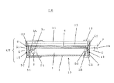
図6乃至図8は、従来の蛍光放電管を使ったエッジライト方式の照明ユニットUTと、これを有する液晶表示装置LDである。この照明ユニットUTは、光を伝達する平板状の透明な導光板1と、この導光板1の4辺のうちの2辺にL字型に曲げられたL字型の蛍光放電管2と、蛍光放電管2から発せられた光を導光板1の端面D1に導く反射シート3が配されている。導光板1と、蛍光放電管2等は筐体9により保持されることにより、照明ユニットUTを形成している。筐体9には、外部にリード線を引き出すためと、筐体9の軽量化のためと、ユーザでの取付固定とを目的として、開口部10が設けられている。開口部10は、照明ユニットUTの外部と通じている。なお、照明ユニットUTの上に液晶パネル11とフロントカバー12が搭載されて液晶表示装置LDとなる(図6)。
【0007】
反射シート3は、導光板1の裏面にも配されており、導光板1の裏面から外へ出る光を再度導光板1の中へ戻し、導光板1の出射面から出る照射光を増大させるという役割を持たせている。また、反射シート3は導光板1の端面のうち、蛍光放電管2の配されていない端面D2に沿うように折り曲げられることにより、導光板1の端面D2まで達した光を反射して、再度導光板1の中へ戻すことで、光の有効利用を図っている場合が多い。さらに、反射シート3は、蛍光放電管2を囲むように配されており、蛍光放電管2から照射される光を導光板1の入射端面D1に向かって反射することでも、光の有効利用を図っている。また、反射シート3の折り曲げ先端部3aは導光板1と両面テープ7によって接着されており、反射シート3が折り曲げによる反発力により垂直に戻ろうとするのを防止している。この反射シート3としては、高反射率を有する白色の樹脂製のフィルムが使用されている。この反射シート3は、図9に示すように、所定形状に裁断されて使用されるとともに、所定箇所に第1の折り返し部S1と第2の折り返し部S2が形成され、これら第1及び第2の折り返し部S1,S2に各々ミシン目が施されて、折り返しやすいように構成されている。なお、反射シート3のL字型の蛍光放電管2が配される側3Aには、2カ所に折り返し部S1,S2が形成され、L字型の蛍光放電管2が配されない側3Bには、1カ所に折り返し部Sが形成される。
【0008】
ここで、反射シート3としては、蛍光放電管2の周囲の部分(この部分を「リフレクタ」と呼ぶこともある。)と導光板1の裏面側の部分とを分離しつつ、両面テープで両者を接着させている構成のものもあるが、図6に示す一体的な構成のもの方が照明ユニットUTの薄型化とコスト及び組立工数の削減をすることができる利点を有する。また、筐体9の外周壁の内側には、導光板1の上方の照射面側に向かって突出する内方側突出部9Aを有するものもある(図5参照)。さらに、反射シート3としては、蛍光放電管2の周囲の部分を円弧形状に囲み、導光板1の照射面側の部分で両面テープ等の接着剤7を介して接着させている構成のものもある。なお、この蛍光放電管2の周囲の部分を円弧形状に囲む反射シート3には、上記ミシン目は施されない。
【0009】
導光板1の照射面側には、光補正シート4が配されている。光補正シート4には、拡散シートやプリズムシート等があり、各種仕様のものを必要に応じて任意枚数設置することにより、導光板から照射される光を拡散する等して、照射光の均斉化と高輝度化を図っている。光補正シート4は、蛍光放電管2を囲む反射シート3Aまで配されているタイプの照明ユニットUTと、導光板1の照射面側の中央にのみ配され、蛍光放電管2を囲む反射シート3Aまで配されていないタイプの照明ユニットもある(図5参照)。
【0010】
導光板1、反射シート3や光補正シート4は、温度変化による熱膨張の寸法差及び製造時の寸法誤差を吸収するために、それぞれの周辺にクリアランスF(F1,F2),F3,F4が設けられている。すなわち、図6に示すように、反射シート3や光補正シート4と筐体9との間には、クリアランスF(F1,F2)、F3,F4が設けられている。ここで、符号Fは、反射シート3の上端部と筐体9の内方側突出部9Aとの間の間隔(クリアランス)を示し、上方側の光補正シート4Aと筐体9の内方側突出部9Aとの間の間隔(クリアランス)をF1として示し、下方側の光補正シート4Aと反射シート3の上端部との間をF2として示す。なお、符号G、G1,G2は、塵埃の進入経路を示し、符号G1は、上記間隔F1への塵埃の進入経路を示し、符号G2は、上記間隔F2への塵埃の進入経路を示す。
【0011】
他方、上記構成の従来の照明ユニットUTを組み立てる製造方法においては、筐体9に、光源2を囲む部分を形成した所定形状の反射シート3を光源2と共に配し、反射シート3の上方に導光板1を配し、導光板1の照射面上に光補正シート4を配する。この場合、反射シート3の上端側の折り曲げ先端部3aは、導光板1の照射面側と両面テープ等の接着剤7を介して接着された後、光補正シート4が配される。その後、照明ユニットUTの上に、透過型や反射型の液晶パネル11が搭載される。
【0012】
【発明が解決しようとする課題】
ところで、上記構成の従来の照明ユニットUT及び液晶表示装置LDにおいては、筐体9の内外の塵埃や、照明ユニットUT及び液晶表示装置LDの組み立て時等に生じる塵埃が液晶パネル11や光補正シート4が配される表示領域側に侵入することを如何に防止するかが大きな問題となっている(図6中の符号G、G1,G2参照)。すなわち、導光板1、光補正シート4や反射シート3の温度変化による熱膨張の寸法差や製造時の寸法誤差を吸収するため、これら間やこれらと筐体9との間には間隔F(F1,F2),F3,F4が設けられているが、筐体9の内部や外部からの塵埃や液晶表示装置LDの組み立て時等に生じる塵埃が、上記各間隔F(F1,F2),F3,F4を介して表示領域側に侵入する危険性がある。また、筐体9の側部には開口部10が設けられているが、この開口部10は上記間隔Fに通じており、このため、開口部10から侵入した塵埃が表示領域側に侵入する。
【0013】
塵埃が表示領域側に侵入すると、出力光を遮り、輝度ムラの原因となったり、また、塵埃と光補正シート4との摩擦により光補正シート4等の表示領域側の部材が損傷する問題が発生する。そして、液晶パネル11と照明ユニットUTの間に塵埃が一度入り込むと、解体せずに取り除くのは非常に困難である。そして、蛍光放電管2が配される側のみならず、蛍光放電管2が配されない側からの塵埃の侵入を防止しなければ有効ではない。
【0014】
また、上記構成の従来の照明ユニットUTにおいては、両面テープ等の接着剤7により導光板1の照射面上に反射シート3の上端側の先端部3aを接着する必要があるため、接着剤7による弊害が生じていた。つまり、接着剤7が導光板の屈折率と異なるため、接着剤7の配される部分では、他の部分よりも輝度が高くなり、輝度むらが生じるという問題を発生させていた。さらに、光補正シート4と導光板1との間に反射シート3の上端側の端部を狭持するように配する必要があるため、反射シート3及び接着剤7の厚さ分(符号F5)、照明ユニットUTが厚くなっていた。
【0015】
このような問題を解決するためには、塵埃の侵入経路に塵埃侵入防止用の部材を別部材として設置する方法が考えられる。しかし、照明ユニットUT及び液晶表示装置LDの軽量小型化を達成するために、導光板1から液晶表示装置LDの外形までの寸法や重量が制約されており、塵埃が侵入することを防止する別部材を導光板1の周囲に設けられない構成となっている。
【0016】
他方、上記構成の従来の照明ユニットUTを組み立てる製造方法においては、反射シート3の上端側の折り曲げ先端部3aを導光板1と両面テープ等の接着剤7を介して接着させる工程が必要であった。また、照明ユニットUT及び液晶表示装置LDの組み立て時において生じる塵埃の侵入は重要な問題であった。
【0017】
そこで、本発明の第1の目的は、照明ユニットや液晶表示装置を構成する部材をそのまま使用して表示領域側への塵埃の侵入を確実に防止するとともに、両面テープ等の接着剤による弊害を防止する照明ユニット及びこの照明ユニットを用いた液晶表示装置を提供することにある。また、本発明の第2の目的は、反射シートの上方側を両面テープ等の接着剤により接着する工程を削減するとともに、簡単な工程で表示領域側への塵埃の侵入を確実に防止する照明ユニットの製造方法及びこの照明ユニットを用いた液晶表示装置の製造方法を提供することにある。
【0018】
本発明の請求項1記載の照明ユニットは、蛍光放電管等の光源と、光源からの光を導光させる導光板と、導光板の照射面側に開口部を有し導光板の裏面側と第1の折り返し部と第2の折り返し部とで光源を囲むようにして配される反射シートと、導光板の照射面側に配される光補正シートと、これらの部材を保持する筐体を備え、前記反射シートの折り曲げ先端部が導光板の照射面にまで及ばず、前記光補正シートの左右両端部が反射シートの折り曲げ先端部に及ぶ大きさとされ、前記反射シートの光源を囲む側の上端側が折り曲げられると共に、この折り曲げ先端部がその折り曲げによる反発力を利用して光補正シートの裏面と接する構成とされていることを特徴とする。
【0019】
この発明によれば、反射シートの折り曲げ先端部がその折り曲げによる反発力を利用して光補正シートの裏面と接するように構成されていることから、別部材を設けなくとも、導光板の照射面と光補正シートとの間隔やその間隔に通じる部分から表示領域側への塵埃の侵入を防止することができるとともに、導光板の照射面側に両面テープ等の接着剤を使用する必要がなくなる。
【0021】
この発明によれば、反射シートは、その折り曲げ先端部が導光板の照射面にまで達していなことと、光補正シートが導光板の照射面上に配されていることから、従来のように光補正シートと導光板との間に反射シートの上端側を挟持するように配する必要がなくなり、光補正シートと導光板との間を狭くすることができる。すなわち、表示領域側にできる間隔を狭くすることができる。なお、表示領域側にできる間隔を狭くできることは、光補正シートと導光板との間に光源が配されていない側から塵埃が表示領域側への侵入も防止できる他、照明ユニットや液晶表示装置の薄型化にも貢献することができる等の種々の利点を有する。
【0023】
この発明によれば、反射シートの折り曲げ先端部がその折り曲げによる反発力を利用して筐体の内方側突出部の裏面と接するように構成されていることから、別部材を設けなくとも、導光板の照射面と光補正シートとの間隔やその間隔に通じる部分から表示領域側への塵埃の侵入が防止されるとともに、導光板の照射面に両面テープ等の接着剤を使用する必要がなくなる。
【0025】
この発明によれば、反射シートは、その折り曲げ先端部が導光板の照射面にまで達していなことと、前記筐体の内方側突出部の裏面の高さ位置が導光板の照射面の高さ位置とされていることから、導光板と筐体の内方側突出部との間を狭くすることができる。すなわち、表示領域側にできる間隔を狭くすることができる。なお、表示領域側にできる間隔を狭くできることは、光補正シートと導光板との間に光源が配されていない側から塵埃が表示領域側へ侵入するのを防止できる他、液晶パネルの薄型化にも貢献することができる等の種々の利点を有する。
【0026】
本発明の請求項3記載の照明ユニットの製造方法は、筐体に、蛍光放電管等の光源を囲む部分を形成した所定形状の反射シートを光源とともに配し、反射シートの照射面側に光源からの光を導光させる導光板を配し、導光板の照射面側に光補正シートを配する照明ユニットの製造方法において、前記反射シートの折り曲げ先端部が導光板の照射面にまで及ばず、前記光補正シートの左右両端部が反射シートの折り曲げ先端部に及ぶ状態で配し、前記反射シートの光源を囲む側の上端側を導光板の照射面側に折り曲げた状態で、前記反射シートの折り曲げ先端部をその折り曲げによる反発力を利用して光補正シートの裏面に接しさせることを特徴とする。
【0027】
この発明によれば、反射シートの上端側を折り曲げた後に、光補正シートを導光板の上方の照射面側に配する際、反射シートの折り曲げ先端部がその反発力によって光補正シートの裏面と接するように構成されていることから、光補正シートの裏面に接するように加工することを目的とした別工程が不要であり、簡単な工程で塵埃の侵入を防止することができる。また、従来のように導光板の照射面側に両面テープ等の接着剤を塗布し反射シートの折り曲げ先端部と導光板を接着させる工程が不要となる。また、本発明による照明ユニットに液晶パネルを搭載する場合には、液晶パネルの荷重が反射シートの反発力に抗して光補正シート及び反射シートの折り曲げ先端部を押圧するため、反射シートは所定の折り曲げ状態に調整される。したがって、反射シートの折り曲げ工程において、反射シートの折り曲げ状態を調整するための工程が不要となる。
【0029】
本発明によれば、反射シートの光源を囲む側の上端側を折り曲げ、この折り曲げ先端部がその折り曲げによる反発力を利用して筐体の内方側突出部の裏面と接するように構成されていることから、筐体の内方側突出部の裏面に接するように加工することを目的とした別工程が不要であり、簡単な工程で塵埃の侵入を防止することができる。また、従来のように導光板の照射面側に両面テープ等の接着剤を塗布し反射シートの折り曲げ先端部と導光板を接着させる工程が不要となる。また、反射シートの折り曲げ先端部を筐体の内方側突出部の裏面に接するように構成させるためには、反射シートの折り曲げ状態を調整しなければならないが、本発明は反射シートを筐体に配置することで筐体の内方側突出部により自然に調整されるため、折り曲げ工程において調整する必要がない。
【0030】
本発明の請求項2記載の液晶表示装置は、蛍光放電管等の光源と、光源からの光を導光させる導光板と、導光板の照射面側に開口部を有し導光板の裏面側と第1の折り返し部と第2の折り返し部とで光源を囲むようにして配される反射シートと、導光板の照射面側に配される光補正シートと、これらの部材を保持する筐体を備えた照明ユニットと、この照明ユニットの照射面側に配される液晶パネルから構成され、前記反射シートの折り曲げ先端部が導光板1の照射面にまで及ばず、前記光補正シートの左右両端部が反射シートの折り曲げ先端部に及ぶ大きさとされ、前記反射シートの光源を囲む側の上端側が折り曲げられると共に、この折り曲げ先端部がその折り曲げによる反発力を利用して光補正シートの裏面と接するとともに、液晶パネルが前記光補正シート及び反射シートを押し下げることで、前記光補正シートが前記導光板の照射面上に配される構成とされていることを特徴とする。
本発明の請求項4記載の液晶表示装置の製造方法は、筐体に、蛍光放電管等の光源を囲む部分を形成した所定形状の反射シートを光源とともに配し、反射シートの照射面側に光源からの光を導光させる導光板を配し、導光板の照射面側に光補正シートを配して照明ユニットとし、この照明ユニットの照射面側に液晶パネルを配する液晶表示装置の製造方法において、前記反射シートの折り曲げ先端部が導光板の照射面にまで及ばず、前記光補正シートの左右両端部が反射シートの折り曲げ先端部に及ぶ状態で配し、
前記反射シートの光源を囲む側の上端側を導光板の照射面側に折り曲げた状態で、前記反射シートの折り曲げ先端部をその折り曲げによる反発力を利用して光補正シートの裏面に接しさせ、前記液晶パネルの荷重により前記反射シートの反発力に反して前記光補正シート及び反射シートを押し下げることで、前記光補正シートを前記導光板の照射面上に配することを特徴とする。
【0031】
本発明によれば、別部材を設けることなく簡単な工程によって、光補正シートと導光板との間に光源が配されていない側から塵埃が表示領域側へ侵入することを防止できるとともに、液晶パネルの薄型化にも貢献することができることから、安価で薄型且つ信頼性の高い照明ユニットを用いた液晶表示装置となる。
【0032】
【発明の実施の形態】
以下、本発明の一実施の形態を図面に基づいて説明する。
【0033】
(第1の実施の形態)
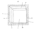
本実施の形態は、図1乃至図3に示すように、光源2と、光源2からの光を伝達する平板上の導光板1と、導光板1の裏面に沿うように配される反射シート3と、導光板1の照射面側に配される光補正シート4と、反射シート3を囲むように間隔を設けて配される筐体9とを備える照明ユニットUTである。光源2は、高周波の交流(例えば、40〜100kHz)で駆動されて発光する蛍光放電管2が導光板1の四辺のうち二辺にL字型に一つ配されている(「L字型の蛍光放電管」と呼ばれる)。
【0034】
筐体9は、導光板1と反射シート3と蛍光放電管2等を左右方向から保持するとともに、液晶パネル11も同時に保持する。このような筐体9としては、各種のものがあり、上下方向から導光板1等を保持するものや、樹脂成形材料から箱形に形成されるものもある。そして、前記筐体9に導光板1や蛍光放電管2等が保持され照明ユニットUTが構成されている。さらに、前記照明ユニットUTに液晶パネル11が搭載され、その上にフロントカバー12が取り付けられて液晶表示装置LDが構成される。なお、上記フロントカバー12も一種の筐体である。また、図中符号11a、11bは、液晶パネル11の一対の基板を示す。なお、上方側の基板11aの内面側にはカラーフィルタが設けられ、下方側の基板11bの内面側には液晶駆動用のパターンが設けられている。
【0035】
導光板1は、光伝達に必要な透過率及び屈折率で代表される光学特性が最適なアクリル等の材料で形成されている。この導光板1には、蛍光放電管2からの距離に応じて形状を変化させたドットパターンあるいは溝パターン(図示せず)等が裏面に施されている。蛍光放電管2から発せられた光は、導光板1の入射側端面D1に集められて内部へと導かれる。
【0036】
導光板1の照射面側には、光補正シート4(4A,4B)が配されている。光補正シート4は、照明ユニットUTの出射光の均斉化と高輝度化を図るためのものであり、本実施の形態では、1枚の拡散シート4Aと1枚のプリズムシート4Bが使用されている。拡散シート4Aは、蛍光放電管2からの光を拡散させ、液晶パネル11を均一に照射するために用いられるシート状の光学部材であり、プリズムシート4Aは、透明の樹脂製フィルムであり、三角形状の規則的な溝を切った構造をしている。光補正シート4は、拡散シート4Aやプリズムシート4Bに限らず、各種仕様のものを必要に応じて任意枚数設置されるが、本発明は仕様及び枚数に制限されることなく適用可能である。また、本実施の形態では、光補正シート4の一部は接着テープにより筐体9に固定されている。これは光補正シート4が振動等により移動して擦れ傷が発生するのを防止するための一部片側のみの仮止めであり、接着位置は蛍光放電管2が配されていない側としている。なお、光補正シート4は、反射シート3、筐体9、さらには導光板1等のいずれにも接着されていないものもある。すなわち、光補正シート4は、枠状の筐体9の側面に位置決めされるのみで、単に積み重ねられているにすぎないものである。いずれの場合も、本発明の作用効果に影響を与えることはない。また、光補正シート4は、導光板1の照射面側の中央にのみ配され、蛍光放電管2を囲む反射シート3Aまで配されていないタイプの照明ユニットもある(図5参照)が、このタイプについては実施例2で説明する。
【0037】
反射シート3は、高反射率を有する白色の樹脂製フィルムが使用されており、反射シート3の裏面から折り曲げられて形成されている。蛍光放電管2を囲むように折り曲げることにより、蛍光放電管2から放射される光を効率よく導光板1の入射端面D1に導く。この反射シート3は、蛍光放電管2を囲む一方側が第1の折り返し部S1から折り曲げられている。そして、この折り返された上端側は、折り曲げられると共に、この折り曲げ先端部3aがその折り曲げによる反発力を利用して光補正シート4の裏面4aと接するように構成されている。なお、反射シート3の厚さは反発力が発揮される厚さであれば、その材質等に応じて任意である。
【0038】
他方、反射シート3蛍光放電管2の配置されていない側3Bは、導光板端面D2に沿うように折り曲げられている。導光体端面D2に沿うように折り曲げられることにより、導光板1の端面D2から出ていく光を再度導光板1内へ戻し、導光板1の表面から出射される光を増やす働きをさせている。導光板1の裏面の反射シート3は、導光板1の裏面から外へ出る光を再度導光板1の中へ戻し出射する照明光を増大させる役割を持たせている。反射シート3の種類としては、上記一体的構成のものの他、蛍光放電管2の周囲の部分(この部分をリフレクタと呼ぶことがある)と導光板1の裏面側の部分を分離したものがあるが、本発明は、このような反射シート3にも適用可能である。
【0039】
上記反射シート3は、図4に示すように、蛍光放電管2が配される側3Aに一条のミシン目S1が施されている。すなわち、従来の図9では、蛍光放電管2が配される側3Aに二条のミシン目S1、S2が施されていたが、第1の折り返し部S1にのみミシン目が施され、第2の折り返し部S2には、ミシン目が施されていないものが使用されている。ここで、第2の折り返し部S2にもミシン目が施されていても良いが、反射シート3の折り曲げ先端部3aの反発力が発揮され易くするためには、第2の折り返し部S2には、ミシン目が施されてない方が好ましい。ただし、反発力に影響与えないものであれば、所定間隔を置いてミシン目を施す等することは実施に応じ任意である。なお、この反射シート3の蛍光放電管2が配されない側3Bは、蛍光放電管2が配される側3Aよりも若干短い。
【0040】
反射シート3の上端側は、折り返され、この折り曲げ先端部3aがその折り曲げによる反発力を利用して光補正シート4の裏面2aと接するように構成されている。これによって、折り曲げ先端部3aと光補正シート4とが密着するため、光補正シート4と導光板1との間に設けられる間隔H1に、蛍光放電管2が配される側から表示領域側への塵埃の侵入が防止されている。そして、反射シート3は、反射シート3自身の反発力を利用して光補正シート4の裏面2aと接しており、導光板1に両面テープ等で接着されることなく配されている。したがって、導光板の照射面側に両面テープ等の接着剤を使用する必要がなくなることにより、両面テープ等の接着剤を原因とする輝度むら等を防止している。
【0041】
反射シート3の上端側の折り曲げ先端部3aは、導光板1の照射面にまで及ばないように配されている。これによって、表示領域側にできる間隔を狭くすることができるため、光補正シート4と導光板1との間H1に蛍光放電管2が配されていない側から塵埃が侵入するのを防止できる他、照明ユニットUT及び液晶表示装置LDの薄型化にも貢献している。なお、反射シート3の光源側3Aの上端側3aは、その反発力を発揮して光補正シート4に接していれば、従来のように導光板1の照射面側に及ぶように設置することは実施に応じ任意である。
【0042】
ここで、従来例で示すように、導光板1、光補正シート4や反射シート3は、温度変化による熱膨張の寸法差及び製造時の寸法誤差を吸収するために、それぞれの周辺に間隔F(F1,F2),F3,F4が設けられている。すなわち、上述したように反射シート3や光補正シート4と筐体9との間には間隔F(F1,F2)、F3,4Fが設けられている。筐体9には、外部にリード線を引き出すためと、筐体の軽量化のためと、ユーザでの取付固定とを目的として、開口部10が設けられ、間隔F(F1,F2)、F3、F4は開口部10を介して照明ユニットUTの外部と通じている。
【0043】
本実施の形態は、上記構成とされるもので、反射シート3の反発力を利用して、導光板1の照射面と光補正シート4との間隔H1や、その間隔に通じる部分F3から表示領域側への塵埃の侵入を防止することができる。特に、外部から塵埃が侵入する筐体の開口部10付近からは塵埃が侵入する可能性が高いため問題となるが、本実施の形態によれば、筐体の開口部10が蛍光放電管2に近い場合は、筐体の開口部10から表示領域側へと通じる間隔F3を塞ぐことができ、表示領域側への塵埃の侵入を防止することができる。また、反射シート3は両面テープ等の接着剤の使用を不要とするため、接着剤を原因とする輝度ムラ等の問題も解決できる。さらに、光補正シート4と導光板1との間に、反射シート3の上端側の折り曲げ先端部3a及び接着剤を挟持するための間隔が不要となるため、光補正シート4と導光板1との間の間隔H1を狭くするか、或いは、無くすことで、照明ユニットUTや液晶表示装置LDの薄型化が図られると共に、補正シート4と導光板1との間の間隔H1に蛍光放電管2が配されていない側からの塵埃の侵入も侵入し難くすることができ、塵埃の大きさによっては、その塵埃の侵入を防止することもできる。
【0044】
また、本発明の光補正シート4は樹脂製フィルムであり、曲がり易いため、反射シート3の反発力により光補正シート4の端部が液晶パネル11側に押し上げられ、液晶パネル11に密着している。したがって、隙間G2から侵入する塵埃を防止することができる。
【0045】
なお、本発明では、反射シート3の先端部3aは光補正シート4Aに接するように説明したが、光補正シート4Aのサイズを小さくして光補正シート4Bに接するように構成した場合や、両光補正シート4(4A,,4B)のサイズを小さくして、液晶パネル13に直接接するように構成した場合にも同様な作用・効果が得られる。
【0046】
(第1の実施の形態の製造方法)
次に、第1の実施の形態の照明ユニットUTを組み立てる場合には、筐体9に蛍光放電管2を囲む部分を形成した所定形状の反射シート3を蛍光放電管2とともに配する。次に、導光板1と蛍光放電管2を反射シート3上の所定の位置に設置させた後、反射シート3の上端側を折り曲げ、この折り曲げた状態で、光補正シート4(4A,4B)を配する。この場合、光補正シート4は、光補正シート4の左右両端部が反射シート3の折り曲げ先端部3aに及ぶ大きさのものを使用する。
【0047】
反射シート3の上端部を折り曲げると、反射シート3の反発力により、元の垂直な形に戻ろうとする力が働く。反射シート3の反発力は光補正シート4を押圧する方向に常に働いているため、この力を利用し、反射シート3をいずれにも接着しない状態で光補正シート4を配することによって、反射シート3の折り曲げ先端部3aが光補正シート4の裏面4aを押圧して密着するようになる。したがって、塵埃の侵入防止を簡単な工程で実現することができる。さらに、従来は、反射シート3を導光板1に両面テープ等の接着剤7で接着する工程を必要としていたが、本実施の形態では必要としないため、この接着工程を削減できる。
【0048】
前記製造方法によって組み立てられた照明ユニットUTに液晶パネル11を搭載する。液晶パネル11を配すると、液晶パネル11はその荷重により反射シート3の反発力に反して光補正シート4及び反射シート3を押し下げ、光補正シート4は導光板1の照射面上に配される。つまり、反射シートの折り曲げ状態は、液晶パネル11の荷重によって自然に調整される。したがって、照明ユニットUTの製造時において反射シート3を調整する工程が不要となり、簡単な工程で本発明の照明ユニットUTを製造することができる。最後に、フロントカバー12を取り付け液晶表示装置LDが完成する。
【0049】
なお、本発明では、反射シート3aは光補正シート4Aに接するように説明したが、光補正シート4のサイズを小さくして光補正シート4Bに接するように構成した場合や、同様にして、液晶パネル13に接するように構成した場合にも同様な効果が得られる。
【0050】
また、本発明では、液晶パネル11の荷重によって、反射シート3の折り曲げ状態が調整されているが、光補正シート4と液晶パネル11の間に筐体9が配される場合は、筐体9の形状によって同様な効果が得られる。
【0051】
(第2の実施の形態)
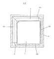
本実施の形態の照明ユニットは、図5に示すように、上記筐体9に、その一部が導光板1の上方の照射面側に突出する内方側突出部9Aを有するが、この内方側突出部9Aは、その裏面9aの高さ位置が導光板1の照射面の高さ位置となるように設けられている。また、光補正シート4(4A,4B)は、導光板1の照射面側の中央に配され、蛍光放電管2を囲む反射シート3Aの位置や蛍光放電管2が配されない側の反射シート3Bまで配されていない。したがって、このタイプの照明ユニットUTにおいては、第1の実施の形態のように、反射シート3の折り曲げ先端部3aをその折り曲げによる反発力を利用して光補正シート4の裏面2aと接するように構成されることができない。
【0052】
そこで、反射シート3の折り曲げ先端部3aは、その折り曲げによる反発力を利用して筐体9の内方側突出部9Aの裏面9aと接するように構成されている。すなわち、反射シート3の折り曲げ先端部3aは、導光板1の照射面D1にまで達しておらず、筐体9の内方側突出部9Aの裏面9aと接するように構成されている。したがって、第1の実施の形態と同様の作用効果が得られる。
【0053】
また、本実施の形態の反射シート3は、筐体9の内方側突出部9Aの裏面9aと接するよう構成されていることから、導光板の照射面と光補正シート4との間の間隔H1やその間隔に通じる部分F3への塵埃の侵入が防止され、従来の両面テープによる輝度ムラの問題もない。しかも、反射シート3の折り曲げ先端部3aを筐体9の内方側突出部9Aの裏面9aと接するよう構成されていることは、光補正シート4が導光板1の照射面側の中央に配され、蛍光放電管2を囲む反射シート3まで配されていないタイプの照明ユニットにおいても、導光板1の照射面と光補正シート4との間隔やその間隔に通じる部分F3から表示領域側への塵埃の侵入を防止することができる。
【0054】
そして、上記構成の照明ユニットUTの上方に液晶パネル11を配されると、液晶パネル11が配される表示領域側の間隔に筐体9の内部や外部からの塵埃が表示領域側に侵入することが防止されることから、薄型で且つ安価で信頼性の高い照明ユニットを用いた液晶表示装置LDとなる。
【0055】
(第2の実施の形態の製造方法)
本実施の形態の照明ユニットの組み立てにおいては、反射シート3の蛍光放電管2を囲む側3Aの上端側を折り曲げた後、内方側突出部9Aを有する筐体9に、蛍光放電管2を囲む部分を形成した所定形状の反射シート3を蛍光放電管2とともに配することによって、この折り曲げ先端部3aの折り曲げによる反発力を利用して筐体9の内方側突出部9Aの裏面に接するように構成させる。その後、反射シート3の照射面側に導光板1を配し、導光板1の照射面側に光補正シート4を配する等は、第1の実施の形態の場合と同様である。この場合、筐体9の内片側突出部9aは、その端部が反射シート3の折り曲げ先端部3aに及ぶように配されている。
【0056】
反射シート3の上端部を折り曲げると、反射シート3の反発力により、元の垂直な形に戻ろうとする力が働く。この反射シート3の反発力は筐体10の内片側突出部9aを押圧する方向に常に働いているため、この力を利用し、反射シート3をいずれにも接着しない状態で光補正シート4を配することによって、反射シート3の折り曲げ先端部3aが光補正シート4の裏面4aを押圧して密着するようになる。したがって、筐体の内方側突出部の裏面に接するように加工することを目的とした別工程が不要であり、簡単な工程で塵埃の侵入を防止することができる。さらに、従来は、反射シート3を導光板1に両面テープ等の接着剤7で接着する工程を必要としていたが、本実施の形態では必要としないため、この接着工程を削減できる。また、筐体9は形状が一定であるため、反射シート3の開口幅3hが反発力によって筐体9の開口幅9h以上となっている場合でも、反射シート3を筐体9に配する際において、反射シート3の反発力に反して反射シート4を押し下げ、反射シート3は筐体9の内部に配される。したがって、前記反発力を利用しない場合は、反射シート3の折り曲げ先端部3aを筐体9の内片側突出部9aに接するように構成させるために反射シート3の折り曲げ状態を調整しなければならないが、本発明によれば、反射シート3を筐体9に配置することで筐体9の形状により自然に調整されるため、折り曲げ工程において調整する必要がなく、塵埃の侵入防止を簡単な工程で実現することができる。
【0057】
【実施例】
ところで、第1及び第2の実施の形態においては、反射シート3が導光板1の照射面にまで及ばないこと、及び両面テープ等の接着剤を使用しないことで光補正シート4と導光板1との間隔H1を狭くするか、又、無くすることにより塵埃の侵入を防止しているが、これは間隔H1においてのみ発揮される効果である。また、実施の形態では光補正シート4が液晶パネル11に密着することにより、隙間G2から侵入する塵埃が防止されているが、光補正シート4が曲がりにくいものである場合は、この効果は得られない。したがって、間隔H1のみならず、光補正シート4と液晶パネル11との間隔H2をも狭くすることにより、さらに塵埃を原因とする表示精度の低下を効果的に防止することができる。そこで、本発明者等は、上記一定の間隔H2を、表示精度に影響を与える塵埃の侵入を防止するために有効な寸法とするため、以下の実験を行った。
【0058】
(実施例1)
光補正シート4と液晶パネル11との間に、0.4mm又は画素寸法の間隔H2を設けて、透過型の液晶パネル11又は反射型の液晶パネル11を搭載した。その結果、前記大きさ以上の塵埃は侵入せず、液晶パネル11の表示に影響を及ぼさなかった。本発明における画素寸法との関係から、前記大きさ以下の塵埃が侵入した場合であれば、画面表示の際に画素を隠すことがなく、表示不良とならないためである。
【0059】
(比較例1)
光補正シート4と液晶パネル11との間に、0.5mm又は画素寸法を超えた間隔H2を設けて、透過型の液晶パネル11又は反射型の液晶パネル11を搭載した。その結果、前記大きさの塵埃が侵入し、液晶パネル11の表示に影響を及ぼした。本発明における画素寸法との関係から、前記大きさ以上の塵埃が侵入した場合は、画面表示の際に画素を隠して表示不良となるためである。
【0060】
上記各実施例から明らかなように、使用する液晶パネル11を0.4mm以下、又は、使用する液晶パネル11の画素寸法以下の間隔で搭載することにより、照明ユニットUT及び液晶表示装置LDにおいて、液晶パネル11の表示に影響を及ぼす塵埃の侵入を確実に防止することができる。したがって、光補正シート4と液晶パネル11との間の間隔H2を、第1の実施の形態において、上記のように構成するように製造した。これにより、間隔H2において少なくとも液晶表示に影響を及ぼすような大きさの塵埃が表示領域側へ侵入することを防止でき、塵埃を原因とする表示精度の低下を効果的に防止することができた。
【0061】
なお、上記間隔で液晶パネル11を搭載することにより、パネル表示面をユーザーが不意の事故で押圧した場合でも、背後に位置する照明ユニットUTが液晶パネル11を受け止めるため、通常ガラスで構成される液晶パネル11が割れてしまう事態も防止することができる。
【0062】
以上、上記各実施の形態では、L字型の蛍光放電管2を使用した照明ユニットUTに本発明を適用した場合について説明したが、本発明は、このL字型でなくとも各種の照明ユニットにも広く適用することができる。また、上記各実施の形態では、反射シート3の光源2が配される側3Aで主に説明したが、本発明は、反射シート3の光源2が配されない側3Bにおいて同様の構成を採用することによっても適用することができる。さらに、反射シート3としては、第1の折り返し部S1を有するもので説明したが、本発明は、光源2の周囲の部分を円弧形状に囲む照明ユニットにも適用することができる。
【0063】
【発明の効果】
本発明の照明ユニット及び液晶表示装置によれば、反射シートの折り曲げ先端部がその折り曲げによる反発力を利用して光補正シートの裏面や筐体の内方側突出部の裏面と接するように構成されていることから、導光板の照射面と光補正シートとの間隔や反射シートと筐体の内方側突出部との間隔やこれらの間隔に通じる部分への塵埃の侵入を防止することが可能となる。また、導光板の照射面側に両面テープ等の接着剤を使用する必要がないため、その分光補正シートと導光板との間隔を狭くすることができるとともに、従来の両面テープによる輝度ムラの問題も解決することが可能となる。
【0064】
本発明の照明ユニットの製造方法及びこの照明ユニットを用いた液晶表示装置の製造方法によれば、反射シートの折り曲げ先端部がその折り曲げによる反発力を利用して光補正シートの裏面や筐体の内方側突出部の裏面と接するように構成することから、簡単な工程で、導光板の照射面と光補正シートとの間隔やその間隔に通じる部分への塵埃の侵入を防止することができる。また、導光板の照射面側に両面テープ等の接着剤を使用する必要がないため、この接着工程を使用することなくなるとともに、接着剤による輝度ムラを防止できる。したがって、表示精度の高い薄型の照明ユニット及びこの照明ユニットを用いた液晶表示装置を簡易な製造方法で製造することが可能となる。
【0065】
【図面の簡単な説明】
【図1】本発明の第1の実施の形態の照明ユニットの構成を示す断面図である。
【図2】上記第1の実施の形態の拡大断面図である。
【図3】上記第1の実施の形態の照明ユニットを示す平面図である。
【図4】上記第1の実施の形態の反射シートを展開して示す平面図である。
【図5】本発明の第2の実施の形態の照明ユニットの構成を示す断面図である。
【図6】従来の照明ユニットの構成を示す断面図である。
【図7】従来の照明ユニットの構成を示す平面図である。
【図8】従来の照明ユニットの側面図である。
【図9】上記従来の反射シートを展開して示す平面図である。
【符号の説明】
1 導光板
2 蛍光放電管(光源)
3,3A,3B 反射シート
3a 反射シートの折り曲げ先端部
4,4A,4B 光補正シート
4a 光補正シートの裏面
9A,9B 筐体の内方側突出部
9a 内方側突出部の裏面
10 筐体の開口部
11 液晶パネル
11a、11b 基板
D1,D2 導光板の入射端面
G,G1,G2 塵埃の進入経路
H1 補正シートと導光板との間の間隔
H2 照明ユニットの出射面上の間隔
S,S1,S2 反射シートの折り返し部
F,F1,F2,F3,F4 反射シート等の周辺の間隔(クリアランス)
F3 反射シート等の周辺の間隔に通じる部分
UT 照明ユニット
LD 液晶表示装置[0001]
BACKGROUND OF THE INVENTION
The present invention relates to an illumination unit in which a light source is arranged on a side surface of a light guide plate and a method for manufacturing the same.,And liquid crystal display device using lighting unitAnd its manufacturing methodAbout.
[0002]
In recent years, display devices for information devices such as notebook personal computers and word processors, or display devices for video devices such as portable televisions, video movies, and car navigation systems have been used for liquid crystal displays, taking advantage of their light weight, thinness, and low power consumption. Many devices have been used. Many of these liquid crystal display devices have a configuration in which illumination light is applied from behind the display element by a built-in illumination unit in order to realize a bright display screen.
[0003]
In this lighting unit, the edge light system in which a light guide plate is placed on the back surface of the display element and a line light source such as a fluorescent discharge tube is arranged on the end face of the light guide plate is characterized by being thin and excellent in luminance uniformity of the light emitting surface. As a backlight method of a liquid crystal display device used for a notebook personal computer or the like, an edge light method is often adopted in consideration of thinness. In liquid crystal display devices used in portable televisions, car navigation systems, etc., in order to achieve both thinness and brightness, an edge light method using two or more fluorescent discharge tubes, or an L-shaped fluorescent discharge tube or There are many cases where the edge light method using the U-shaped fluorescent discharge tube is adopted.
[0004]
The fluorescent discharge tube is driven by high-frequency alternating current to emit light, and lead wires are connected to both ends in order to supply a predetermined drive voltage to the fluorescent discharge tube from the outside. A connector is provided at the tip of these two lead wires and connected to an external inverter.
[0005]
In the edge light system, a fluorescent discharge tube is arranged outside the light guide plate. In order to further extend the characteristics of the liquid crystal display device such as portability and space saving, members such as the light guide plate and the fluorescent discharge tube are used. The point is how to arrange it compactly in the lighting unit and the liquid crystal display device.
[0006]
6 to 8 show an edge light type illumination unit UT using a conventional fluorescent discharge tube and a liquid crystal display device LD having the same. The illumination unit UT includes a flat transparent
[0007]
The
[0008]
Here, as the
[0009]
A
[0010]
The
[0011]
On the other hand, in the manufacturing method for assembling the conventional lighting unit UT having the above-described configuration, the reflecting
[0012]
[Problems to be solved by the invention]
By the way, in the conventional illumination unit UT and liquid crystal display device LD having the above-described configuration, the dust inside and outside the
[0013]
When dust enters the display area side, the output light is blocked, resulting in uneven brightness, and the members on the display area side such as the
[0014]
Further, in the conventional lighting unit UT having the above-described configuration, it is necessary to bond the tip 3 a on the upper end side of the
[0015]
In order to solve such a problem, a method of installing a member for preventing dust intrusion as a separate member in the dust intrusion path is conceivable. However, in order to achieve a lighter and smaller size of the illumination unit UT and the liquid crystal display device LD, the size and weight from the
[0016]
On the other hand, in the manufacturing method for assembling the conventional lighting unit UT having the above-described configuration, a step of bonding the bent leading end portion 3a on the upper end side of the
[0017]
Accordingly, the first object of the present invention is to reliably prevent the intrusion of dust into the display area by using the members constituting the lighting unit and the liquid crystal display device as they are and to prevent the harmful effects caused by the adhesive such as the double-sided tape. An object of the present invention is to provide an illumination unit for preventing the liquid crystal display device using the illumination unit. In addition, the second object of the present invention is to reduce the process of adhering the upper side of the reflection sheet with an adhesive such as a double-sided tape, and to reliably prevent dust from entering the display area by a simple process. Unit manufacturing methodAnd manufacturing method of liquid crystal display device using the illumination unitIs to provide.
[0018]
Of the present inventionThe lighting unit according to
[0019]
According to this invention, since the bending tip end portion of the reflection sheet is configured to contact the back surface of the light correction sheet using the repulsive force of the bending, the irradiation surface of the light guide plate can be provided without providing a separate member. It is possible to prevent the dust from entering the display area from the space between the light correction sheet and the light correction sheet, and it is not necessary to use an adhesive such as a double-sided tape on the irradiation surface side of the light guide plate.
[0021]
According to the present invention, the reflection sheet has a bent tip portion that does not reach the irradiation surface of the light guide plate, and the light correction sheet is disposed on the irradiation surface of the light guide plate. It is not necessary to arrange the upper end side of the reflection sheet between the light correction sheet and the light guide plate, and the space between the light correction sheet and the light guide plate can be narrowed. That is, the space that can be formed on the display area side can be reduced. Note that the space that can be formed on the display area side can be reduced because dust can also be prevented from entering the display area side from the side where the light source is not disposed between the light correction sheet and the light guide plate, as well as an illumination unit and a liquid crystal display device. It has various advantages such as being able to contribute to the reduction in thickness.
[0023]
According to the present invention, since the bent leading end portion of the reflection sheet is configured to contact the back surface of the inwardly protruding portion of the housing using the repulsive force due to the bending, even if no separate member is provided, The distance between the irradiation surface of the light guide plate and the light correction sheet and the intrusion of dust from the portion leading to the interval to the display area side are prevented, and it is necessary to use an adhesive such as a double-sided tape on the irradiation surface of the light guide plate Disappear.
[0025]
According to this invention, the reflection sheet has a bent leading end portion that does not reach the irradiation surface of the light guide plate, and the height position of the back surface of the inwardly protruding portion of the housing is that of the irradiation surface of the light guide plate. Since the height is set, the space between the light guide plate and the inward protruding portion of the housing can be narrowed. That is, the space that can be formed on the display area side can be reduced. Note that the distance that can be reduced on the display area side can be reduced by preventing dust from entering the display area side from the side where the light source is not disposed between the light correction sheet and the light guide plate, and reducing the thickness of the liquid crystal panel. It has various advantages, such as being able to contribute.
[0026]
Of the present inventionClaim3The manufacturing method of the lighting unit described in the housing,Such as fluorescent discharge tubesA reflective sheet having a predetermined shape that forms a portion surrounding the light source is arranged together with the light source, a light guide plate that guides light from the light source is disposed on the irradiation surface side of the reflection sheet, and a light correction sheet is disposed on the irradiation surface side of the light guide plate. In the manufacturing method of the lighting unit to be arranged,The bent front end portion of the reflection sheet does not reach the irradiation surface of the light guide plate, and the left and right end portions of the light correction sheet are arranged in a state reaching the bent front end portion of the reflection sheet,Reflective sheetofIn a state where the upper end side of the side surrounding the light source is bent to the irradiation surface side of the light guide plate,SaidIt is characterized in that the bent leading end portion of the reflection sheet is brought into contact with the back surface of the light correction sheet using a repulsive force by the bending.
[0027]
According to the present invention, when the light correction sheet is disposed on the irradiation surface side above the light guide plate after the upper end side of the reflection sheet is bent, the bent front end portion of the reflection sheet and the back surface of the light correction sheet by the repulsive force. Since it is configured so as to be in contact, a separate process for processing so as to be in contact with the back surface of the light correction sheet is unnecessary, and dust can be prevented from entering by a simple process. Moreover, the process of apply | coating adhesives, such as a double-sided tape, to the irradiation surface side of a light-guide plate like the past, and adhere | attaching the bending front-end | tip part of a reflective sheet and a light-guide plate becomes unnecessary. Further, when the liquid crystal panel is mounted on the lighting unit according to the present invention, since the load of the liquid crystal panel presses the light correction sheet and the bent leading end portion of the reflection sheet against the repulsive force of the reflection sheet, the reflection sheet is predetermined. It is adjusted to the bent state. Therefore, a step for adjusting the bent state of the reflection sheet is not required in the reflection sheet bending step.
[0029]
According to the present invention, the upper end side of the reflective sheet surrounding the light source is bent, and the bent tip is configured to contact the back surface of the inward protruding portion of the housing using the repulsive force of the bending. Therefore, there is no need for a separate process for processing so as to be in contact with the back surface of the inner projecting portion of the housing, and dust can be prevented from entering by a simple process. Moreover, the process of apply | coating adhesives, such as a double-sided tape, to the irradiation surface side of a light-guide plate like the past, and adhere | attaching the bending front-end | tip part of a reflective sheet and a light-guide plate becomes unnecessary. Further, in order to configure the bent leading end portion of the reflective sheet so as to be in contact with the back surface of the inwardly protruding portion of the casing, the bent state of the reflective sheet must be adjusted. Since it adjusts naturally by the inward protrusion part of a housing | casing by arrange | positioning in, it is not necessary to adjust in a bending process.
[0030]
Claims of the invention2The described liquid crystal display deviceSuch as fluorescent discharge tubesA light source, a light guide plate for guiding light from the light source, and a light guide plateIrradiation sideHas an opening inOn the back side of the light guide plate, the first folded portion, and the second folded portionA reflection sheet disposed so as to surround the light source, a light correction sheet disposed on the irradiation surface side of the light guide plate, an illumination unit including a housing that holds these members, and an irradiation surface side of the illumination unit. Composed of LCD panels,The bent front end portion of the reflection sheet does not reach the irradiation surface of the
According to a fourth aspect of the present invention, there is provided a method of manufacturing a liquid crystal display device, wherein a reflective sheet having a predetermined shape formed with a portion surrounding a light source such as a fluorescent discharge tube is disposed in a casing together with the light source, and on the irradiation surface side of the reflective sheet. Manufacture of a liquid crystal display device in which a light guide plate for guiding light from a light source is provided, a light correction sheet is provided on the irradiation surface side of the light guide plate to form an illumination unit, and a liquid crystal panel is provided on the irradiation surface side of the illumination unit In the method, the bent tip of the reflection sheet does not reach the irradiation surface of the light guide plate, and the right and left ends of the light correction sheet are arranged in a state reaching the bent tip of the reflection sheet,
In the state where the upper end side of the side surrounding the light source of the reflection sheet is bent to the irradiation surface side of the light guide plate, the bending tip of the reflection sheet is brought into contact with the back surface of the light correction sheet using the repulsive force of the bending, The light correction sheet is arranged on an irradiation surface of the light guide plate by pressing down the light correction sheet and the reflection sheet against a repulsive force of the reflection sheet by a load of the liquid crystal panel.
[0031]
According to the present invention, dust can be prevented from entering the display area side from the side where the light source is not disposed between the light correction sheet and the light guide plate by a simple process without providing a separate member, and the liquid crystal Since it can contribute to the thinning of the panel, a liquid crystal display device using an inexpensive, thin and highly reliable lighting unit is obtained.
[0032]
DETAILED DESCRIPTION OF THE INVENTION
Hereinafter, an embodiment of the present invention will be described with reference to the drawings.
[0033]
(First embodiment)
In the present embodiment, as shown in FIGS. 1 to 3, a
[0034]
The
[0035]
The
[0036]
The light correction sheet 4 (4A, 4B) is disposed on the irradiation surface side of the
[0037]
The
[0038]
On the other hand, the
[0039]
As shown in FIG. 4, the
[0040]
The upper end side of the
[0041]
The bent front end portion 3 a on the upper end side of the
[0042]
Here, as shown in the conventional example, the
[0043]
The present embodiment is configured as described above, and uses the repulsive force of the
[0044]
Further, since the
[0045]
In the present invention, the front end portion 3a of the
[0046]
(Manufacturing method of the first embodiment)
Next, when assembling the illumination unit UT of the first embodiment, a reflecting
[0047]
When the upper end portion of the
[0048]
The liquid crystal panel 11 is mounted on the lighting unit UT assembled by the manufacturing method. When the liquid crystal panel 11 is disposed, the liquid crystal panel 11 pushes down the
[0049]
In the present invention, the reflection sheet 3a has been described as being in contact with the
[0050]
In the present invention, the bent state of the
[0051]
(Second Embodiment)
As shown in FIG. 5, the lighting unit of the present embodiment has an inner
[0052]
Therefore, the bent leading end portion 3a of the
[0053]
Moreover, since the
[0054]
When the liquid crystal panel 11 is disposed above the illumination unit UT having the above configuration, dust from inside or outside the
[0055]
(Manufacturing method of the second embodiment)
In assembling the lighting unit of the present embodiment, the upper end side of the
[0056]
When the upper end portion of the
[0057]
【Example】
By the way, in 1st and 2nd embodiment, the
[0058]
(Example 1)
A transmissive liquid crystal panel 11 or a reflective liquid crystal panel 11 was mounted between the
[0059]
(Comparative Example 1)
A transmissive liquid crystal panel 11 or a reflective liquid crystal panel 11 was mounted between the
[0060]
As is clear from each of the above embodiments, by mounting the liquid crystal panel 11 to be used at an interval of 0.4 mm or less or less than the pixel size of the liquid crystal panel 11 to be used, in the illumination unit UT and the liquid crystal display device LD, Intrusion of dust that affects the display of the liquid crystal panel 11 can be reliably prevented. Therefore, the space H2 between the
[0061]
Since the liquid crystal panel 11 is mounted at the above-described interval, the lighting unit UT located behind the user receives the liquid crystal panel 11 even when the user presses the panel display surface due to an unexpected accident. The situation where the liquid crystal panel 11 breaks can also be prevented.
[0062]
As described above, in each of the above embodiments, the case where the present invention is applied to the illumination unit UT using the L-shaped
[0063]
【The invention's effect】
According to the illumination unit and the liquid crystal display device of the present invention, the bent front end portion of the reflection sheet is configured to contact the back surface of the light correction sheet or the back surface of the inward protruding portion of the housing using the repulsive force of the bending. Therefore, it is possible to prevent the intrusion of dust into the interval between the irradiation surface of the light guide plate and the light correction sheet, the interval between the reflection sheet and the inwardly protruding portion of the housing, and the portion communicating with these intervals. It becomes possible. Moreover, since it is not necessary to use an adhesive such as a double-sided tape on the irradiation surface side of the light guide plate, the distance between the spectral correction sheet and the light guide plate can be narrowed, and the problem of uneven brightness due to the conventional double-sided tape Can also be solved.
[0064]
Manufacturing method of lighting unit of the present inventionAnd manufacturing method of liquid crystal display device using the illumination unitAccording to the present invention, the bending tip of the reflecting sheet is configured to contact the back surface of the light correction sheet and the back surface of the inward protruding portion of the housing using the repulsive force of the bending. It is possible to prevent the intrusion of dust into the interval between the irradiation surface of the light guide plate and the light correction sheet and the portion leading to the interval. Further, since it is not necessary to use an adhesive such as a double-sided tape on the irradiation surface side of the light guide plate, this bonding process is not used, and uneven brightness due to the adhesive can be prevented. Therefore, a thin lighting unit with high display accuracyAnd liquid crystal display device using the illumination unitCan be manufactured by a simple manufacturing method.
[0065]
[Brief description of the drawings]
FIG. 1 is a cross-sectional view showing a configuration of a lighting unit according to a first embodiment of the present invention.
FIG. 2 is an enlarged cross-sectional view of the first embodiment.
FIG. 3 is a plan view showing the illumination unit according to the first embodiment.
FIG. 4 is a plan view showing an unfolded reflection sheet of the first embodiment.
FIG. 5 is a cross-sectional view showing a configuration of a lighting unit according to a second embodiment of the present invention.
FIG. 6 is a cross-sectional view showing a configuration of a conventional lighting unit.
FIG. 7 is a plan view showing a configuration of a conventional illumination unit.
FIG. 8 is a side view of a conventional lighting unit.
FIG. 9 is a plan view showing the conventional reflective sheet in a developed state.
[Explanation of symbols]
1 Light guide plate
2 Fluorescent discharge tube (light source)
3,3A, 3B Reflective sheet
3a Bending tip of reflective sheet
4,4A, 4B Light correction sheet
4a Back side of light correction sheet
9A, 9B Inner side protruding part of housing
9a Back side of inward protruding part
10 Opening of housing
11 LCD panel
11a, 11b substrate
D1, D2 Incident end face of light guide plate
G, G1, G2 Dust entry path
H1 Distance between the correction sheet and the light guide plate
H2 Distance on the exit surface of the lighting unit
S, S1, S2 Reflection sheet folding part
F, F1, F2, F3, F4 Peripheral spacing (clearance) of reflective sheet, etc.
F3 A part that leads to the surrounding space, such as a reflective sheet
UT lighting unit
LD liquid crystal display
Claims (4)
前記反射シートの折り曲げ先端部が導光板の照射面にまで及ばず、前記光補正シートの左右両端部が反射シートの折り曲げ先端部に及ぶ大きさとされ、
前記反射シートの光源を囲む側の上端側が折り曲げられると共に、この折り曲げ先端部がその折り曲げによる反発力を利用して光補正シートの裏面と接する構成とされていることを特徴とする照明ユニット。 A light source such as a fluorescent discharge tube , a light guide plate for guiding light from the light source, an opening on the irradiation surface side of the light guide plate, a back surface side of the light guide plate, a first folded portion, and a second folded portion; in comprising a reflecting sheet disposed so as to surround the light source, and an optical compensation sheet disposed on the irradiation surface side of the light guide plate, a housing for holding these members,
The bending tip of the reflection sheet does not reach the irradiation surface of the light guide plate, and the right and left ends of the light correction sheet are sized to reach the bending tip of the reflection sheet,
An illumination unit, wherein an upper end side of the reflecting sheet surrounding the light source is bent, and a bent leading end portion is in contact with a back surface of the light correction sheet using a repulsive force by the bending.
前記反射シートの折り曲げ先端部が導光板の照射面にまで及ばず、前記光補正シートの左右両端部が反射シートの折り曲げ先端部に及ぶ大きさとされ、
前記反射シートの光源を囲む側の上端側が折り曲げられると共に、この折り曲げ先端部がその折り曲げによる反発力を利用して光補正シートの裏面と接するとともに、液晶パネルが前記光補正シート及び反射シートを押し下げることで、前記光補正シートが前記導光板の照射面上に配される構成とされていることを特徴とする液晶表示装置。 A light source such as a fluorescent discharge tube , a light guide plate for guiding light from the light source, an opening on the irradiation surface side of the light guide plate, a back surface side of the light guide plate, a first folded portion, and a second folded portion; A light source sheet, a light correction sheet disposed on the irradiation surface side of the light guide plate, an illumination unit including a housing for holding these members, and an irradiation surface side of the illumination unit. It consists of a liquid crystal panel
The bending tip of the reflection sheet does not reach the irradiation surface of the light guide plate, and the right and left ends of the light correction sheet are sized to reach the bending tip of the reflection sheet,
Light source with the upper end of the side is bent surrounding the reflecting sheet, together with contact with the rear surface of the optical compensation sheet the bent tip by using the repulsive force due to bending thereof, the liquid crystal panel pushes the optical compensation sheet and the reflection sheet it is, liquid crystal display device, characterized in that said optical correction sheet is configured to be disposed on the irradiated surface of the light guide plate.
前記反射シートの折り曲げ先端部が導光板の照射面にまで及ばず、前記光補正シートの左右両端部が反射シートの折り曲げ先端部に及ぶ状態で配し、
前記反射シートの光源を囲む側の上端側を導光板の照射面側に折り曲げた状態で、前記反射シートの折り曲げ先端部をその折り曲げによる反発力を利用して光補正シートの裏面に接しさせることを特徴とする照明ユニットの製造方法。A reflective sheet having a predetermined shape in which a portion surrounding a light source such as a fluorescent discharge tube is formed is disposed in the housing together with the light source, and a light guide plate for guiding light from the light source is disposed on the irradiation surface side of the reflective sheet. In the manufacturing method of the illumination unit which arrange | positions the light correction sheet | seat 4 to the irradiation surface side,
The bent front end of the reflection sheet does not reach the irradiation surface of the light guide plate, and the left and right ends of the light correction sheet are arranged in a state reaching the bent front end of the reflection sheet,
In a folded state the upper end of the side surrounding the light source of the reflective sheet to the irradiated surface side of the light guide plate, be in contact with the back surface of the optical compensation sheet utilizing the repulsive force due to the bending of the bent tip portion of the reflecting sheet The manufacturing method of the lighting unit characterized by these.
前記反射シートの折り曲げ先端部が導光板の照射面にまで及ばず、前記光補正シートの左右両端部が反射シートの折り曲げ先端部に及ぶ状態で配し、The bent front end portion of the reflection sheet does not reach the irradiation surface of the light guide plate, and the left and right end portions of the light correction sheet are arranged in a state reaching the bent front end portion of the reflection sheet,
前記反射シートの光源を囲む側の上端側を導光板の照射面側に折り曲げた状態で、前記反射シートの折り曲げ先端部をその折り曲げによる反発力を利用して光補正シートの裏面に接しさせ、前記液晶パネルの荷重により前記反射シートの反発力に反して前記光補正シート及び反射シートを押し下げることで、前記光補正シートを前記導光板の照射面上に配することを特徴とする液晶表示装置の製造方法。In the state where the upper end side of the side surrounding the light source of the reflection sheet is bent to the irradiation surface side of the light guide plate, the bending tip of the reflection sheet is brought into contact with the back surface of the light correction sheet using the repulsive force of the bending, A liquid crystal display device, wherein the light correction sheet is disposed on an irradiation surface of the light guide plate by pressing down the light correction sheet and the reflection sheet against a repulsive force of the reflection sheet by a load of the liquid crystal panel. Manufacturing method.
Priority Applications (1)
| Application Number | Priority Date | Filing Date | Title |
|---|---|---|---|
| JP2000027605A JP4439656B2 (en) | 2000-02-04 | 2000-02-04 | LIGHTING UNIT AND ITS MANUFACTURING METHOD, AND LIQUID CRYSTAL DISPLAY DEVICE USING THE LIGHTING UNIT AND ITS MANUFACTURING METHOD |
Applications Claiming Priority (1)
| Application Number | Priority Date | Filing Date | Title |
|---|---|---|---|
| JP2000027605A JP4439656B2 (en) | 2000-02-04 | 2000-02-04 | LIGHTING UNIT AND ITS MANUFACTURING METHOD, AND LIQUID CRYSTAL DISPLAY DEVICE USING THE LIGHTING UNIT AND ITS MANUFACTURING METHOD |
Publications (2)
| Publication Number | Publication Date |
|---|---|
| JP2001216827A JP2001216827A (en) | 2001-08-10 |
| JP4439656B2 true JP4439656B2 (en) | 2010-03-24 |
Family
ID=18553152
Family Applications (1)
| Application Number | Title | Priority Date | Filing Date |
|---|---|---|---|
| JP2000027605A Expired - Fee Related JP4439656B2 (en) | 2000-02-04 | 2000-02-04 | LIGHTING UNIT AND ITS MANUFACTURING METHOD, AND LIQUID CRYSTAL DISPLAY DEVICE USING THE LIGHTING UNIT AND ITS MANUFACTURING METHOD |
Country Status (1)
| Country | Link |
|---|---|
| JP (1) | JP4439656B2 (en) |
Families Citing this family (10)
| Publication number | Priority date | Publication date | Assignee | Title |
|---|---|---|---|---|
| AU2003221004A1 (en) * | 2002-03-29 | 2003-10-13 | Matsushita Electric Industrial Co., Ltd. | Illumination unit and liquid crystal display apparatus comprising same |
| AU2002330301A1 (en) * | 2002-09-18 | 2004-04-08 | Matsushita Electric Industrial Co., Ltd. | Illumination unit and liquid crystal display comprising it |
| AU2002330310A1 (en) | 2002-09-19 | 2004-04-08 | Matsushita Electric Industrial Co., Ltd. | Illumination unit and liquid crystal display comprising it |
| JPWO2004111977A1 (en) | 2003-06-13 | 2006-07-27 | 東芝松下ディスプレイテクノロジー株式会社 | Flat panel display |
| JP4486795B2 (en) * | 2003-06-30 | 2010-06-23 | オプトレックス株式会社 | Light unit |
| US9316805B2 (en) * | 2010-11-23 | 2016-04-19 | Southpac Trust International Inc, Trustee of the LDH Trust | Frameless light modifying element |
| CN103090255B (en) * | 2011-10-27 | 2015-06-03 | 群康科技(深圳)有限公司 | Display device and backlight module thereof |
| JP2013239335A (en) * | 2012-05-15 | 2013-11-28 | Sharp Corp | Backlight unit and liquid crystal display device |
| JP6036187B2 (en) * | 2012-11-05 | 2016-11-30 | 三菱電機株式会社 | Planar light source device and display device using the same |
| CN115097668B (en) * | 2022-07-25 | 2023-08-25 | 业成科技(成都)有限公司 | Backlight source diaphragm group preparation method, backlight module and display structure |
-
2000
- 2000-02-04 JP JP2000027605A patent/JP4439656B2/en not_active Expired - Fee Related
Also Published As
| Publication number | Publication date |
|---|---|
| JP2001216827A (en) | 2001-08-10 |
Similar Documents
| Publication | Publication Date | Title |
|---|---|---|
| JP3845349B2 (en) | Backlight and liquid crystal display device | |
| JP5173640B2 (en) | Backlight unit and method for assembling the same | |
| WO2003083362A1 (en) | Illumination unit and liquid crystal display apparatus comprising same | |
| JP4707260B2 (en) | LIGHTING UNIT, ITS MANUFACTURING METHOD, AND LIQUID CRYSTAL DISPLAY DEVICE USING THE LIGHTING UNIT | |
| CN102621744B (en) | Liquid crystal display device | |
| JP2003255309A (en) | Optical unit and liquid crystal display using the same | |
| CN112882290B (en) | Backlight module and display device | |
| WO2003056236A1 (en) | Illumination unit and liquid crystal display device using the unit | |
| JP3666265B2 (en) | Lighting unit and liquid crystal display device using the same | |
| TWI595295B (en) | Display device | |
| WO2005098312A1 (en) | Lighting unit and liquid crystal display unit using this | |
| JP4439656B2 (en) | LIGHTING UNIT AND ITS MANUFACTURING METHOD, AND LIQUID CRYSTAL DISPLAY DEVICE USING THE LIGHTING UNIT AND ITS MANUFACTURING METHOD | |
| KR101630342B1 (en) | Liquid crystal display device and mathod for manufacturing the same | |
| JP2002279820A (en) | Lighting unit and liquid crystal display unit using the same | |
| JP2002174811A (en) | Liquid crystal display device | |
| WO2019184412A1 (en) | Backlight module and liquid crystal display device | |
| JP3434227B2 (en) | Illumination unit and liquid crystal display device using the same | |
| JP2004253187A (en) | Lighting unit and liquid crystal display using the same | |
| JP5087148B2 (en) | Liquid crystal display | |
| JP2006086132A (en) | Lighting system and liquid crystal display | |
| JP2001330817A (en) | Liquid crystal display device and method of manufacture | |
| US8704968B2 (en) | Liquid crystal display | |
| JP4309598B2 (en) | Illumination unit and liquid crystal display device using the same | |
| TWI825920B (en) | Backlight module, display device, and method of assembling backlight module | |
| CN218767391U (en) | Side-in backlight module, display device and electronic equipment |
Legal Events
| Date | Code | Title | Description |
|---|---|---|---|
| A711 | Notification of change in applicant |
Free format text: JAPANESE INTERMEDIATE CODE: A711 Effective date: 20061110 |
|
| A521 | Written amendment |
Free format text: JAPANESE INTERMEDIATE CODE: A523 Effective date: 20070112 |
|
| A621 | Written request for application examination |
Free format text: JAPANESE INTERMEDIATE CODE: A621 Effective date: 20070126 |
|
| A977 | Report on retrieval |
Free format text: JAPANESE INTERMEDIATE CODE: A971007 Effective date: 20090204 |
|
| A131 | Notification of reasons for refusal |
Free format text: JAPANESE INTERMEDIATE CODE: A131 Effective date: 20090210 |
|
| A521 | Written amendment |
Free format text: JAPANESE INTERMEDIATE CODE: A523 Effective date: 20090409 |
|
| TRDD | Decision of grant or rejection written | ||
| A01 | Written decision to grant a patent or to grant a registration (utility model) |
Free format text: JAPANESE INTERMEDIATE CODE: A01 Effective date: 20091214 |
|
| A01 | Written decision to grant a patent or to grant a registration (utility model) |
Free format text: JAPANESE INTERMEDIATE CODE: A01 |
|
| A61 | First payment of annual fees (during grant procedure) |
Free format text: JAPANESE INTERMEDIATE CODE: A61 Effective date: 20100106 |
|
| FPAY | Renewal fee payment (event date is renewal date of database) |
Free format text: PAYMENT UNTIL: 20130115 Year of fee payment: 3 |
|
| R150 | Certificate of patent or registration of utility model |
Ref document number: 4439656 Country of ref document: JP Free format text: JAPANESE INTERMEDIATE CODE: R150 Free format text: JAPANESE INTERMEDIATE CODE: R150 |
|
| S531 | Written request for registration of change of domicile |
Free format text: JAPANESE INTERMEDIATE CODE: R313531 |
|
| FPAY | Renewal fee payment (event date is renewal date of database) |
Free format text: PAYMENT UNTIL: 20130115 Year of fee payment: 3 |
|
| R350 | Written notification of registration of transfer |
Free format text: JAPANESE INTERMEDIATE CODE: R350 |
|
| S533 | Written request for registration of change of name |
Free format text: JAPANESE INTERMEDIATE CODE: R313533 |
|
| FPAY | Renewal fee payment (event date is renewal date of database) |
Free format text: PAYMENT UNTIL: 20130115 Year of fee payment: 3 |
|
| R350 | Written notification of registration of transfer |
Free format text: JAPANESE INTERMEDIATE CODE: R350 |
|
| FPAY | Renewal fee payment (event date is renewal date of database) |
Free format text: PAYMENT UNTIL: 20140115 Year of fee payment: 4 |
|
| R250 | Receipt of annual fees |
Free format text: JAPANESE INTERMEDIATE CODE: R250 |
|
| R250 | Receipt of annual fees |
Free format text: JAPANESE INTERMEDIATE CODE: R250 |
|
| R250 | Receipt of annual fees |
Free format text: JAPANESE INTERMEDIATE CODE: R250 |
|
| R250 | Receipt of annual fees |
Free format text: JAPANESE INTERMEDIATE CODE: R250 |
|
| R250 | Receipt of annual fees |
Free format text: JAPANESE INTERMEDIATE CODE: R250 |
|
| LAPS | Cancellation because of no payment of annual fees |