JP4422843B2 - Scan exposure equipment - Google Patents
Scan exposure equipment Download PDFInfo
- Publication number
- JP4422843B2 JP4422843B2 JP2000023784A JP2000023784A JP4422843B2 JP 4422843 B2 JP4422843 B2 JP 4422843B2 JP 2000023784 A JP2000023784 A JP 2000023784A JP 2000023784 A JP2000023784 A JP 2000023784A JP 4422843 B2 JP4422843 B2 JP 4422843B2
- Authority
- JP
- Japan
- Prior art keywords
- master
- slave
- speed
- exposure
- switching
- Prior art date
- Legal status (The legal status is an assumption and is not a legal conclusion. Google has not performed a legal analysis and makes no representation as to the accuracy of the status listed.)
- Expired - Fee Related
Links
Images


Description
【0001】
【発明の属する技術分野】
本発明はガラスプレート又はシリコンウエハ上に形成される電子回路パターンの露光を短時間に効率よく行える露光装置に関するものである。
【0002】
【従来の技術】
液晶パネルなどのデバイスを製造するためには、露光装置によってガラスプレート上に微細な電子回路を形成している。昨今、液晶パネルの大型化に伴い、これらの製造に使用される露光装置はマスクステージとプレートステージを同期してスキャン露光する装置が注目を集めてきた。
【0003】
従来のスキャン露光装置に関しては、特開平9−69481号公報に記載されているように、応答性の低い駆動系をマスタとし、応答性の高いマスクステージ側の駆動系をスレーブとして制御するマスタ・スレーブ同期制御方式を取っているものがある。
【0004】
マスタ・スレーブ同期制御方式においては、図6に示すように、マスタの駆動系は速度指令値を生成するマスタ速度指令値生成器50及び速度指令に追従すべく動作する速度制御手段の速度比較器51と速度補償器52等を有する構成とともにその制御対象の速度情報v1と積分器54により得られる位置情報y1を出力するものである。
【0005】
スレーブ駆動系はマスタ制御系の速度情報v1を速度指令値として入力し、それに追従すべく動作する速度制御系の速度比較器61と速度補償器62等、及びスレーブ側で同期検出されたマスタ・スレーブ相対位置を位置比較器60で検出し、積分器64より得られるスレーブ側位置情報y2をマスタ側位置情報y1に追従すべく動作する位置制御系を有し、これらの構成によりマスタ・スレーブ両駆動系を同期スキャンさせ露光処理を行っていた。なお、図6において57及び67は位置補償器を示している。
【0006】
【発明が解決しようとする課題】
しかしながら上記従来例では、マスタ・スレーブ制御系において、同期スキャン露光終了後マスタ・スレーブ間のスキャン方向相対位置が同期スキャン中とは大きく異なる位置に移動しようとする場合、ステージを一旦停止とし、マスタ・スレーブの同期を切り、2軸のステージを別々に駆動させ目的の位置に移動させる必要があった。このため、装置のタクトタイムが低下する原因となっていた。
本発明は、上記従来の露光装置におけるタクトタイムが低下する原因をなくして、高い同期精度を維持しつつ、同期スキャン露光終了後、ステージを一旦停止させることなく次のステージ位置に移動させて、装置及び製造ライン全体としてのスループット向上に寄与することができる露光装置を提供することを目的とする。
【0007】
【課題を解決するための手段】
上記目的を達成するため、本発明では、個別に操作可能な2つの制御対象をそれぞれ駆動制御する2つの制御系を有し、応答性の低い駆動系をマスタとし、応答性の高い駆動系をスレーブとしたマスタ・スレーブ制御系を構成する露光装置であって、マスタの駆動系はマスタ系速度指令値生成器で生成される速度指令値に追従すべく動作する速度制御系を有すると共にその制御対象の速度情報と位置情報を出力するものであり、スレーブの駆動系は、スレーブ系速度指令値生成器で生成される速度指令値または前記マスタの駆動系から出力される速度情報のうち、第1切り替え手段によって選択されたいずれか一方に追従すべく動作する速度制御系と、前記スレーブ系速度指令値生成器から得られる位置指令値または前記マスタの駆動系から出力される位置情報にオフセットを加えた値のうち、第2切り替え手段によって選択されたいずれか一方に追従すべく動作する位置制御系とを備え、前記第1および第2切り替え手段によって前記マスタの駆動系から出力される情報が選択されることによって、前記マスタの駆動系と前記スレーブの駆動系は同期制御され、前記同期駆動中に予め指定された位置で切り替え手段を切り替えることによって、両駆動系の同期が切り離されて個別に駆動されることを特徴とする。
【0008】
【発明の実施の形態および作用】
本発明の実施の形態に係る露光装置は、同期スキャン時には従来マスタ側に1つしかなかった速度指令値生成器をマスタ・スレーブの両方に用意し、露光区間においては、従来通りマスタ側はマスタ側速度指令値生成器に追従し、スレーブ側はマスタに追従するような制御を行い、露光区間を終了した時点においては、直ちにスレーブ側をスレーブ側速度指令値生成器に追従させる様に切り替える。この切り替えは、マスタ位置情報と、予め露光範囲から計算した同期切り替え位置を比較することにより行う。また、切り替えに際して、スレーブ系の速度偏差、位置偏差の増大を招かないために同期区間においてもマスタ系速度指令値生成器に対してマスタ・スレーブ間の相対位置オフセット分加算された値をスレーブ系速度指令値生成器においても同時に発生させておく。これによって、スムーズな信号切り替えが行われ、ステージを停止させることなくマスタ・スレーブ同期を切り離し、各駆動系個別の制御に切り替えることが可能となることを特徴とする。
【0009】
上記構成によって、同期スキャン露光後、その次のショット(shot)の露光準備位置やホーム(Home)位置に移動する際に、一旦ステージを停止させることがなくなるため、ステージの加減速により発生する処理時間の低下を招くことなく連続した露光動作を行うことが可能となる。
【0010】
【実施例】
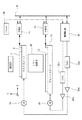
以下に本発明の実施例について添付の図面を参照しながら詳しく説明する。図1は本発明の実施例に係るスキャン露光装置を示す基本的な構成図である。図1において1はフォトマスクであり、このフォトマスク1には液晶パネルの回路パターンが形成されている。2はフォトマスク1を搭載するマスクステージであり、図示しないヨー(Yaw)ガイドに沿ってY方向に駆動可能な構造となっている。マスクステージ2のスキャン方向位置はレーザ干渉計3aによって計測し、その計測結果は通信バス31を介してステージ制御回路30に転送される。そして、この露光装置は、ステージ制御回路30においてマスクステージリニアモータ4aへの出力電流指令値を計算し、D/A変換器32a及び電力増幅器33aを介してマスクステージリニアモータ4aを駆動している。
ミラー光学系20は凹面鏡と凸面鏡で構成されており、円弧状に等倍率でその結像面に像を結像する。
【0011】
12は表面にレジストが塗布されているガラスプレートであり、先の露光工程で形成された複数個の被露光領域(ショット)が配列されている。11はガラスプレート12を搭載するプレートステージである。このプレートステージ11は、ガラスプレート12を受けて上面に吸着・固定するチャック、X軸方向及びY軸方向に水平移動するXYステージ、ミラー光学系20の光軸方向であるΖ軸方向への移動、Z軸に平行な軸の周りに回転可能な回転ステージ等を備えて構成され、マスク1に形成されている回路パターンをガラスプレート12上に合致させるための6軸構成となっている。
【0012】
プレートステージ11のスキャン方向位置はレーザ干渉計3bによって測定し、その測定結果は通信バス31を介してステージ制御回路30に転送される。ステージ制御回路30は、プレートステージリニアモータ4bへの出力電流指令値を計算し、D/A変換器32b及び電力増幅器33bを介してプレートステージリニアモータ4bを駆動制御している。なお、図1において、34はクロックを示している。
【0013】
図2は本来制御回路内で実現される制御構成を示したものである。なお、ここでは、応答性が低いプレートステージ11側をマスタ、マスクステージ2側をスレーブとすることにする。同期制御構成を示した図2では、各軸の位置情報をy1、y2、速度情報をv1、v2とし、2軸同期化を目指した制御構成を示すものである。以降、信号の流れに従って説明を行う。まず、この制御系では2つの制御モードを有しており、破線で囲んで示した信号選択器107で制御モードが切り替えられる。
【0014】
速度指令値はその生成器108aにより作られてマスタ系に入力される。同期駆動時には、この指令値はマスタ系にのみ入力され、スレーブ系には直接作用させない構成となっている。比較器104aにより速度指令値は速度v1と比較され、その偏差信号はその速度補償器102aに入力される。速度補償器102aの出力が、マスタ系のD/A変換器32b、電力増幅器33bを経てマスタ側リニアモータ4bへ入力される操作量となる。マスタ系の動特性101aは伝達関数Q1で表しており、速度補償器伝達関数Cvと合わせて速度制御系マイナーループが構成される。103aは積分器を表しており速度v1と対応する位置y1との関係を示したものである。ここまでマスタ系を説明したがスレーブ系に関しても同様であり、符番も対応させてある。
【0015】
すなわち、速度指令値はその生成器108bにより作られてスレーブ系に入力される。同期駆動時には、この指令値はスレーブ系にのみ入力され、マスタ系には直接作用させない構成となっている。比較器104bにより速度指令値は速度v2と比較され、その偏差信号はその速度補償器102bに入力される。速度補償器102bの出力が、スレーブ系のD/A変換器32a、電力増幅器33aを経てスレーブ側リニアモータ4aへ入力される操作量となる。スレーブ系の動特性101bは伝達関数Q1で表しており、速度補償器伝達関数Cvと合わせて速度制御系マイナループが構成される。103bは積分器を表しており速度v2と対応する位置y2との関係を示したものである。
【0016】
以下、実際の露光シーケンスに即した同期制御の切り替えにつき説明する。
図3はスキャン露光装置における露光シーケンスを示したフローチャートである。このフローチャートにおいては先の露光工程で形成されたパターンに合わせて露光を行う第2露光工程(2ndLayer)のシーケンスを示している。この第2露光工程においては、タクトタイム向上のため、第1ショット(1stShot)から第nショットの順でアライメント計測を先に行い、全ショットのアライメント計測が終了後、第nショットから第1ショットの順で露光を行う。すなわちステップ22で最終ショット(第nショット)か否かを判断し、最終ショットでないときにはステップ23でステップ(Step)状の駆動を行う。ステップ24ではアライメント計測を行い、最終の第nショットまでステップ22〜24が繰り返される。最終ショットがなされた後は、ステップ25へ進み、露光における最終ショットである第1ショット(1stShot)か否かが判断され、第1ショットでなければ露光及びステップ(Step)が行われ(ステップ26)、第1ショットに至るまで繰り返される。第1ショットに達したら、露光及びホーム(Home)位置移動がなされる(ステップ27)。
【0017】
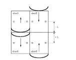
図4は、ショット数が4のガラスプレートを例にとり、ガラスプレート12上でのショットレイアウトと露光方向の関係を示している。ここで、矢印の向きはガラスプレート12上でのミラー光学系スリット面の相対的な移動方向を示している。同図において、各ショット中心間のY方向距離を2Lとすると、ショット4(shot4)、ショット3(shot3)においてのマスク1に対してのプレート相対位置は+L、ショット1(shot1)、ショット2(shot2)においてのマスク1に対してのプレート相対位置は−Lとなる。
【0018】
図5は第3ショット露光後第2ショット露光準備位置へ移動する際のマスタ、スレーブ各軸の最適な駆動パターンを示す図である。区間A〜Bは第3ショット(3rdShot)露光区間であり、マスタ・スレーブ2軸が同期して駆動され、区間B〜Cは同期を切り、この区間では別々な目標位置を目指して駆動が行われることになる。
【0019】
さてここで、マスタ・スレーブ同期制御切り替えのポイントはマスタ系スレーブ系間の関係であり、図2における信号選択器107の設定とその切り替えタイミングとなる。
【0020】
図5に示す区間A〜Bは同期区間であり、図2において両軸間で伝達される情報は速度v1と位置y1の2点であり、切り替えのための信号選択器107はa方向にセットしておく。この状態で、速度信号v1はスレーブ系の速度制御マイナループへの指令値として伝達される。位置信号y1にマスタ・スレーブ間相対位置オフセット110として+Lを加算したものと、スレーブ系位置y2と比較され、その偏差、すなわち同期誤差がスレーブ系位置補償器104bに入力され、同期制御が行われる。
【0021】
図5における区間B〜Cはマスタ、スレーブ非同期区間であり、Cにおいてマスタに対してスレーブの相対位置が−Lとなるように各ステージが駆動される。C点は第2ショット(2ndShot)の露光準備位置でのマスタ・スレーブのステージ位置関係となる。
【0022】
B点を通過した瞬間において図2に示す信号選択器107をb方向にセットすることにより、マスタ・スレーブ同期は切り離されて、2軸は個別の目標位置に駆動することになる。
【0023】
信号切り替えのタイミングはスキャン方向及びマスタ側位置情報y1と同期切り替え位置109を比較することにより作り出すことが出来る。
また、信号の切り替えに際しては、切り替えのタイミングによりスレーブ系の速度偏差及び位置偏差の増大を招き制御系のエラーを起こしてしまう恐れがあるためスムーズな信号切り替えが必要となってくる。そこで、図5に示すA点からの駆動開始の際にマスタ系速度指令値生成器108aとともにスレーブ系速度指令値生成器108bを初期化し、同期区間ではマスタ系速度指令値生成器108aに対して+L分のオフセットが加算された値をスレーブ系速度指令値生成器108bでも同時に発生させておく。もちろん、同期区間においては、スレーブ系速度指令値生成器の出力をスレーブ制御系には入力してはならない。
【0024】
以上はスキャン露光後、その次のショットに移動する際の処理を例にとって説明したが、最終ショットスキャン露光終了後、ホーム位置へ移動する際も同等であり、本実施例によりスキャン露光終了時ステージを一旦停止させることなく次のショットの露光準備位置に移動でき、装置タクトタイムの向上を実現することが出来る。
【0025】
【デバイス生産方法の実施例】
次に上記説明した露光装置または露光方法を利用したデバイスの生産方法の実施例を説明する。
図7は微小デバイス(ICやLSI等の半導体チップ、液晶パネル、CCD、薄膜磁気ヘッド、マイクロマシン等)の製造のフローを示す図である。ステップ1(回路設計)ではデバイスのパターン設計を行う。ステップ2(マスク製作)では設計したパターンを形成したマスクを製作する。一方、ステップ3(ウエハ製造)ではシリコンやガラス等の材料を用いてウエハを製造する。ステップ4(ウエハプロセス)は前工程と呼ばれ、上記用意したマスクとウエハを用いて、リソグラフィ技術によってウエハ上に実際の回路を形成する。次のステップ5(組み立て)は後工程と呼ばれ、ステップ4によって作製されたウエハを用いて半導体チップ化する工程であり、アッセンブリ工程(ダイシング、ボンディング)、パッケージング工程(チップ封入)等の工程を含む。ステップ6(検査)ではステップ5で作製された半導体デバイスの動作確認テスト、耐久性テスト等の検査を行う。こうした工程を経て半導体デバイスが完成し、これが出荷(ステップ7)される。
【0026】
図8は上記ウエハプロセスの詳細なフローを示す図である。ステップ11(酸化)ではウエハの表面を酸化させる。ステップ12(CVD)ではウエハ表面に絶縁膜を形成する。ステップ13(電極形成)ではウエハ上に電極を蒸着によって形成する。ステップ14(イオン打込み)ではウエハにイオンを打ち込む。ステップ15(レジスト処理)ではウエハに感光剤を塗布する。ステップ16(露光)では上記説明した露光装置によりマスクの回路パターンをウエハに焼付露光する。ステップ17(現像)では露光したウエハを現像する。ステップ18(エッチング)では現像したレジスト像以外の部分を削り取る。ステップ19(レジスト剥離)ではエッチングが済んで不要となったレジストを取り除く。これらのステップを繰り返し行うことにより、ウエハ上に多重に回路パターンが形成される。
【0027】
本実施例の生産方法を用いれば、従来は製造が難しかった高集積度のデバイスを低コストに製造することができる。
【0028】
【発明の効果】
以上説明したように、本発明によれば、高い同期精度を維持しつつ、同期スキャン露光終了後一旦停止させることなく次のステージ位置に移動できるため、装置及び製造ライン全体としてのスループット向上に寄与することが出来る。
【図面の簡単な説明】
【図1】 本発明の第一の実施例に係わる同期スキャン露光装置を示す構成図である。
【図2】 本発明に実施例に係わり本来制御回路内で実現される制御構成を示したブロック図である。
【図3】 本発明の実施例に係わる露光シーケンスを示したフローチャートである。
【図4】 本発明の実施例に係わるガラスプレート上でのショットレイアウトと露光方向を示した図である。
【図5】 図4における第3ショット露光後、第2ショット露光準備位置へ移動する際のマスタ、スレーブ各軸の最適な駆動パターンである。
【図6】 従来例の制御構成を示すブロック図である。
【図7】 微小デバイスの製造の流れを示す図である。
【図8】 図7におけるウエハプロセスの詳細な流れを示す図である。
【符号の説明】
1:フォトマスク、2:マスクステージ、3:レーザ干渉計、4:リニアモータ、11:プレートステージ、12:ガラスプレート、20:ミラー光学系、30:ステージ制御回路、31:通信バス、32:DAC(D/A変換器)、101:軸の特性、102:速度補償器、103:積分器、104:速度比較器、105:位置補償器、106:位置比較器、107:信号選択器(切り替え手段)、108:速度指令値生成器、109:同期切り替え位置、110:マスタ・スレーブ間相対位置オフセット、v1,v2:速度情報、y1,y2:位置情報。[0001]
BACKGROUND OF THE INVENTION
The present invention relates to an exposure apparatus that can efficiently perform exposure of an electronic circuit pattern formed on a glass plate or a silicon wafer in a short time.
[0002]
[Prior art]
In order to manufacture a device such as a liquid crystal panel, a fine electronic circuit is formed on a glass plate by an exposure apparatus. In recent years, with the increase in size of liquid crystal panels, an exposure apparatus used for manufacturing these devices has attracted attention as an apparatus that performs scanning exposure by synchronizing a mask stage and a plate stage.
[0003]
As for a conventional scanning exposure apparatus, as described in Japanese Patent Application Laid-Open No. 9-69481, a master that controls a driving system with low responsiveness as a master and a driving system on the mask stage side with high responsiveness as a slave. Some have taken the slave synchronous control method.
[0004]
In the master-slave synchronous control system, as shown in FIG. 6, the master drive system has a master speed
[0005]
The slave drive system inputs the speed information v1 of the master control system as a speed command value, and the
[0006]
[Problems to be solved by the invention]
However, in the above-mentioned conventional example, in the master / slave control system, when the relative position in the scanning direction between the master and the slave is about to move to a position that is significantly different from that during the synchronous scan after the synchronous scan exposure, the stage is temporarily stopped and the master・ Slave synchronization was required, and the two-axis stage had to be driven separately and moved to the target position. For this reason, the tact time of the apparatus has been reduced.
The present invention eliminates the cause of a decrease in tact time in the conventional exposure apparatus, maintains high synchronization accuracy, and moves to the next stage position without stopping the stage after the synchronous scan exposure is completed. An object of the present invention is to provide an exposure apparatus that can contribute to an improvement in throughput of the apparatus and the entire production line.
[0007]
[Means for Solving the Problems]
To achieve the above object, the present onset bright, has two control system for driving and controlling each individually operable two controlled object, and master less responsive drive system, highly responsive driving An exposure apparatus constituting a master / slave control system with a system as a slave, the master drive system having a speed control system that operates to follow the speed command value generated by the master system speed command value generator and outputs a position information and speed information of the object to be controlled, the slave drive system, of the velocity information outputted from the driving system of the speed command value or the master which is generated by the slave system speed command value generator , a speed control system which operates to follow either selected by the first switching hands stage, the driving system of the position command or the master obtained from the slave system speed instruction value generator Of the force is a value obtained by adding the offset to the position information is, the master by a second switch and a position control system which operates to follow either selected by the hand stage, the first and second switching means by the information output from the drive system is selected, the drive system of the slave and the drive system of the master are controlled synchronously, to switch the toggle means in a pre-specified position during the synchronous driving I it, the synchronization of the two drive system is disconnected in and said Rukoto are individually driven to.
[0008]
BEST MODE FOR CARRYING OUT THE INVENTION
In the exposure apparatus according to the embodiment of the present invention, the speed command value generator, which has been conventionally only one on the master side at the time of synchronous scanning, is prepared for both the master and the slave. The slave side follows control of the side speed command value generator, and the slave side performs control to follow the master. When the exposure period ends, the slave side is immediately switched to follow the slave side speed command value generator. This switching is performed by comparing the master position information with the synchronous switching position calculated in advance from the exposure range. In addition, when switching, in order not to increase the speed deviation and position deviation of the slave system, the value obtained by adding the relative position offset between the master and slave to the master system speed command value generator is also obtained in the slave system even during the synchronization period. The speed command value generator is also generated at the same time. Thus, smooth signal switching is performed, and master-slave synchronization can be disconnected without stopping the stage, and switching to individual control of each drive system is possible.
[0009]
With the above configuration, after the synchronous scan exposure, when moving to the exposure preparation position or home position of the next shot (shot), the stage is not temporarily stopped. It is possible to perform a continuous exposure operation without causing a decrease in time.
[0010]
【Example】
Hereinafter, embodiments of the present invention will be described in detail with reference to the accompanying drawings. FIG. 1 is a basic block diagram showing a scan exposure apparatus according to an embodiment of the present invention. In FIG. 1, 1 is a photomask, and a circuit pattern of a liquid crystal panel is formed on the
The mirror
[0011]
[0012]
The scanning direction position of the
[0013]
FIG. 2 shows a control configuration originally realized in the control circuit. Here, the
[0014]
The speed command value is generated by the
[0015]
That is, the speed command value is generated by the
[0016]
Hereinafter, switching of synchronization control in accordance with an actual exposure sequence will be described.
FIG. 3 is a flowchart showing an exposure sequence in the scanning exposure apparatus. This flowchart shows a second exposure step (2nd Layer) sequence in which exposure is performed in accordance with the pattern formed in the previous exposure step. In this second exposure step, in order to improve the tact time, the alignment measurement is performed in the order from the first shot (1stshot) to the nth shot. After the alignment measurement of all shots is completed, the nth shot to the first shot are performed. The exposure is performed in this order. That is, it is determined in
[0017]
FIG. 4 shows the relationship between the shot layout on the
[0018]
FIG. 5 is a diagram showing an optimum drive pattern for each axis of the master and slave when moving to the second shot exposure preparation position after the third shot exposure. Sections A to B are the third shot (3rdshot) exposure section, and the master and slave 2 axes are driven synchronously, sections B to C are disconnected, and driving is performed aiming at different target positions in this section. It will be.
[0019]
Now, the point of master / slave synchronization control switching is the relationship between the master and slave systems, which is the setting of the
[0020]
Sections A to B shown in FIG. 5 are synchronous sections. In FIG. 2, information transmitted between both axes is two points of speed v1 and position y1, and the
[0021]
Sections B to C in FIG. 5 are master and slave asynchronous sections. In C, each stage is driven so that the relative position of the slave to the master is −L. Point C is the master / slave stage position relationship at the exposure preparation position of the second shot (2ndshot).
[0022]
When the
[0023]
The signal switching timing can be generated by comparing the scanning direction and master side position information y1 with the
Further, when switching signals, smooth signal switching is required because there is a risk of an increase in the speed deviation and position deviation of the slave system depending on the switching timing, resulting in an error in the control system. Therefore, the slave system speed
[0024]
The above is an example of processing when moving to the next shot after scan exposure, but the same applies when moving to the home position after the end of the final shot scan exposure. Can be moved to the exposure preparation position for the next shot without stopping, and the apparatus tact time can be improved.
[0025]
[Example of device production method]
Next, an embodiment of a device production method using the above-described exposure apparatus or exposure method will be described.
FIG. 7 is a diagram showing a flow of manufacturing a microdevice (a semiconductor chip such as an IC or LSI, a liquid crystal panel, a CCD, a thin film magnetic head, a micromachine, etc.). In step 1 (circuit design), a device pattern is designed. In step 2 (mask production), a mask on which the designed pattern is formed is produced. On the other hand, in step 3 (wafer manufacture), a wafer is manufactured using a material such as silicon or glass. Step 4 (wafer process) is called a pre-process, and an actual circuit is formed on the wafer by lithography using the prepared mask and wafer. The next step 5 (assembly) is referred to as a post-process, and is a process for forming a semiconductor chip using the wafer produced in
[0026]
FIG. 8 shows a detailed flow of the wafer process. In step 11 (oxidation), the wafer surface is oxidized. In step 12 (CVD), an insulating film is formed on the wafer surface. In step 13 (electrode formation), an electrode is formed on the wafer by vapor deposition. In step 14 (ion implantation), ions are implanted into the wafer. In step 15 (resist process), a photosensitive agent is applied to the wafer. In step 16 (exposure), the circuit pattern of the mask is printed on the wafer by exposure using the exposure apparatus described above. In step 17 (development), the exposed wafer is developed. In step 18 (etching), portions other than the developed resist image are removed. In step 19 (resist stripping), unnecessary resist after etching is removed. By repeatedly performing these steps, multiple circuit patterns are formed on the wafer.
[0027]
By using the production method of this embodiment, a highly integrated device that has been difficult to manufacture can be manufactured at low cost.
[0028]
【The invention's effect】
As described above, according to the present invention, it is possible to move to the next stage position without stopping once after completion of synchronous scan exposure while maintaining high synchronization accuracy, which contributes to improvement of throughput of the apparatus and the entire production line. I can do it.
[Brief description of the drawings]
FIG. 1 is a block diagram showing a synchronous scan exposure apparatus according to a first embodiment of the present invention.
FIG. 2 is a block diagram showing a control configuration originally realized in the control circuit according to the embodiment of the present invention.
FIG. 3 is a flowchart showing an exposure sequence according to an embodiment of the present invention.
FIG. 4 is a view showing a shot layout and an exposure direction on a glass plate according to an embodiment of the present invention.
5 is an optimum drive pattern for each axis of the master and slave when moving to the second shot exposure preparation position after the third shot exposure in FIG. 4. FIG.
FIG. 6 is a block diagram showing a control configuration of a conventional example.
FIG. 7 is a diagram showing a flow of manufacturing a microdevice.
8 is a diagram showing a detailed flow of the wafer process in FIG. 7. FIG.
[Explanation of symbols]
1: Photomask, 2: Mask stage, 3: Laser interferometer, 4: Linear motor, 11: Plate stage, 12: Glass plate, 20: Mirror optical system, 30: Stage control circuit, 31: Communication bus, 32: DAC (D / A converter), 101: axis characteristic, 102: speed compensator, 103: integrator, 104: speed comparator, 105: position compensator, 106: position comparator, 107: signal selector ( Switching means), 108: speed command value generator, 109: synchronization switching position, 110: master-slave relative position offset, v1, v2: speed information, y1, y2: position information.
Claims (4)
マスタの駆動系はマスタ系速度指令値生成器で生成される速度指令値に追従すべく動作する速度制御系を有すると共にその制御対象の速度情報と位置情報を出力するものであり、
スレーブの駆動系は、スレーブ系速度指令値生成器で生成される速度指令値または前記マスタの駆動系から出力される速度情報のうち、第1切り替え手段によって選択されたいずれか一方に追従すべく動作する速度制御系と、前記スレーブ系速度指令値生成器から得られる位置指令値または前記マスタの駆動系から出力される位置情報にオフセットを加えた値のうち、第2切り替え手段によって選択されたいずれか一方に追従すべく動作する位置制御系とを備え、
前記第1および第2切り替え手段によって前記マスタの駆動系から出力される情報が選択されることによって、前記マスタの駆動系と前記スレーブの駆動系は同期制御され、
前記同期駆動中に予め指定された位置で切り替え手段を切り替えることによって、両駆動系の同期が切り離されて個別に制御されることを特徴とするスキャン露光装置。Configures a master / slave control system that has two control systems that drive and control two controllable objects that can be operated individually, with the low-responsive drive system as the master and the high-responsive drive system as the slave. An exposure apparatus,
The master drive system has a speed control system that operates to follow the speed command value generated by the master system speed command value generator, and outputs speed information and position information of the controlled object.
Slave drive system, of the velocity information outputted from the speed command value or the drive system of the master that is generated in the slave system speed command value generator, to follow either selected by the first switching hands stage to a speed control system which operates, among the values obtained by adding the offset to the position information output from a driving system of the position command or the master obtained from the slave system speed instruction value generator, selected by the second switching hands stage is provided with a position control system which operates to follow either,
Wherein by information output from a driving system of the master is selected by the first and second switching means, the drive system of the the drive system of the master-slave is controlled synchronously,
The I by the switching the toggle means in a pre-designated position in synchronization during driving, the synchronization of the two drive systems is disconnected is controlled individually scan exposure apparatus according to claim Rukoto.
Priority Applications (1)
| Application Number | Priority Date | Filing Date | Title |
|---|---|---|---|
| JP2000023784A JP4422843B2 (en) | 2000-02-01 | 2000-02-01 | Scan exposure equipment |
Applications Claiming Priority (1)
| Application Number | Priority Date | Filing Date | Title |
|---|---|---|---|
| JP2000023784A JP4422843B2 (en) | 2000-02-01 | 2000-02-01 | Scan exposure equipment |
Publications (3)
| Publication Number | Publication Date |
|---|---|
| JP2001217176A JP2001217176A (en) | 2001-08-10 |
| JP2001217176A5 JP2001217176A5 (en) | 2007-03-15 |
| JP4422843B2 true JP4422843B2 (en) | 2010-02-24 |
Family
ID=18549894
Family Applications (1)
| Application Number | Title | Priority Date | Filing Date |
|---|---|---|---|
| JP2000023784A Expired - Fee Related JP4422843B2 (en) | 2000-02-01 | 2000-02-01 | Scan exposure equipment |
Country Status (1)
| Country | Link |
|---|---|
| JP (1) | JP4422843B2 (en) |
-
2000
- 2000-02-01 JP JP2000023784A patent/JP4422843B2/en not_active Expired - Fee Related
Also Published As
| Publication number | Publication date |
|---|---|
| JP2001217176A (en) | 2001-08-10 |
Similar Documents
| Publication | Publication Date | Title |
|---|---|---|
| US6359677B2 (en) | Stage apparatus, exposure apparatus using the same, and a device manufacturing method | |
| US20050156552A1 (en) | Driving apparatus, exposure apparatus, and device manufacturing method | |
| US7319283B2 (en) | Moving apparatus, exposure apparatus, and device manufacturing method | |
| US7016049B2 (en) | Alignment apparatus, control method therefor, exposure apparatus, device manufacturing method, semiconductor manufacturing factory, and exposure apparatus maintenance method | |
| JPWO2005036620A1 (en) | Exposure method, exposure apparatus, and device manufacturing method | |
| US20090002659A1 (en) | Stage apparatus, exposure apparatus, and method of manufacturing device | |
| KR100516689B1 (en) | Driving apparatus, exposure apparatus, and device manufacturing method | |
| JP4422843B2 (en) | Scan exposure equipment | |
| JP2000260696A (en) | Stage control method, exposing method, aligner and fabrication of device | |
| US5838443A (en) | Exposure apparatus implementing priority speed setting arrangement | |
| JPH1126365A (en) | Method and apparatus for projection exposure | |
| US20030128345A1 (en) | Scanning type exposure apparatus and a device manufacturing method using the same | |
| EP3945368A1 (en) | Exposing apparatus and method for manufacturing article | |
| JP3595708B2 (en) | Exposure apparatus, device manufacturing method, and control method | |
| JP3227089B2 (en) | Positioning stage apparatus, exposure apparatus using the same, and device manufacturing method | |
| JP3244872B2 (en) | Exposure apparatus and device manufacturing method using the same | |
| JP3722330B2 (en) | Exposure apparatus and device manufacturing method | |
| US6122059A (en) | Scanning exposure apparatus and device fabrication method in which multiple laser interferometers use a respective laser head | |
| JP2000164506A (en) | Exposure method and aligner | |
| JP2005142583A (en) | Stage apparatus, aligner, method of manufacturing device, and method of driving stage | |
| JPH1187233A (en) | Projection aligner | |
| JP7022527B2 (en) | Stage equipment, lithography equipment, and article manufacturing methods | |
| JP2005109522A (en) | Stage device, exposure device, and device manufacturing method, and stage driving method | |
| JP2000294479A (en) | Scanning alighner and device manufacture | |
| JP3244871B2 (en) | Exposure apparatus and device manufacturing method using the same |
Legal Events
| Date | Code | Title | Description |
|---|---|---|---|
| A521 | Written amendment |
Free format text: JAPANESE INTERMEDIATE CODE: A523 Effective date: 20070129 |
|
| A621 | Written request for application examination |
Free format text: JAPANESE INTERMEDIATE CODE: A621 Effective date: 20070129 |
|
| RD01 | Notification of change of attorney |
Free format text: JAPANESE INTERMEDIATE CODE: A7421 Effective date: 20090406 |
|
| A977 | Report on retrieval |
Free format text: JAPANESE INTERMEDIATE CODE: A971007 Effective date: 20091001 |
|
| TRDD | Decision of grant or rejection written | ||
| A01 | Written decision to grant a patent or to grant a registration (utility model) |
Free format text: JAPANESE INTERMEDIATE CODE: A01 Effective date: 20091201 |
|
| A01 | Written decision to grant a patent or to grant a registration (utility model) |
Free format text: JAPANESE INTERMEDIATE CODE: A01 |
|
| A61 | First payment of annual fees (during grant procedure) |
Free format text: JAPANESE INTERMEDIATE CODE: A61 Effective date: 20091207 |
|
| FPAY | Renewal fee payment (event date is renewal date of database) |
Free format text: PAYMENT UNTIL: 20121211 Year of fee payment: 3 |
|
| R150 | Certificate of patent or registration of utility model |
Free format text: JAPANESE INTERMEDIATE CODE: R150 |
|
| FPAY | Renewal fee payment (event date is renewal date of database) |
Free format text: PAYMENT UNTIL: 20131211 Year of fee payment: 4 |
|
| LAPS | Cancellation because of no payment of annual fees |