JP4410574B2 - System and method for injecting test jitter into a data bitstream - Google Patents
System and method for injecting test jitter into a data bitstream Download PDFInfo
- Publication number
- JP4410574B2 JP4410574B2 JP2004025173A JP2004025173A JP4410574B2 JP 4410574 B2 JP4410574 B2 JP 4410574B2 JP 2004025173 A JP2004025173 A JP 2004025173A JP 2004025173 A JP2004025173 A JP 2004025173A JP 4410574 B2 JP4410574 B2 JP 4410574B2
- Authority
- JP
- Japan
- Prior art keywords
- voltage
- jitter
- current
- output
- differential
- Prior art date
- Legal status (The legal status is an assumption and is not a legal conclusion. Google has not performed a legal analysis and makes no representation as to the accuracy of the status listed.)
- Expired - Lifetime
Links
- 238000012360 testing method Methods 0.000 title claims description 19
- 238000000034 method Methods 0.000 title description 35
- 239000003990 capacitor Substances 0.000 claims description 28
- 230000004044 response Effects 0.000 claims description 17
- 230000001360 synchronised effect Effects 0.000 claims 1
- 101150096622 Smr2 gene Proteins 0.000 description 17
- 239000000872 buffer Substances 0.000 description 15
- 238000002347 injection Methods 0.000 description 7
- 239000007924 injection Substances 0.000 description 7
- 230000001419 dependent effect Effects 0.000 description 6
- 230000008569 process Effects 0.000 description 6
- 230000008901 benefit Effects 0.000 description 5
- 238000007599 discharging Methods 0.000 description 5
- 230000007704 transition Effects 0.000 description 4
- 230000007423 decrease Effects 0.000 description 3
- 238000010586 diagram Methods 0.000 description 3
- 239000000203 mixture Substances 0.000 description 3
- 230000003213 activating effect Effects 0.000 description 2
- 230000008859 change Effects 0.000 description 2
- 230000003247 decreasing effect Effects 0.000 description 2
- 230000000694 effects Effects 0.000 description 2
- 239000000835 fiber Substances 0.000 description 2
- 238000005259 measurement Methods 0.000 description 2
- 238000004891 communication Methods 0.000 description 1
- 238000010276 construction Methods 0.000 description 1
- 238000013461 design Methods 0.000 description 1
- 238000004519 manufacturing process Methods 0.000 description 1
- 239000000463 material Substances 0.000 description 1
- 238000000691 measurement method Methods 0.000 description 1
- 230000007246 mechanism Effects 0.000 description 1
- 229910044991 metal oxide Inorganic materials 0.000 description 1
- 150000004706 metal oxides Chemical class 0.000 description 1
- 238000012986 modification Methods 0.000 description 1
- 230000004048 modification Effects 0.000 description 1
- 230000000630 rising effect Effects 0.000 description 1
- 239000004065 semiconductor Substances 0.000 description 1
- 238000006467 substitution reaction Methods 0.000 description 1
- 238000010998 test method Methods 0.000 description 1
- 238000012546 transfer Methods 0.000 description 1
- 239000002699 waste material Substances 0.000 description 1
Images


Classifications
-
- H—ELECTRICITY
- H04—ELECTRIC COMMUNICATION TECHNIQUE
- H04L—TRANSMISSION OF DIGITAL INFORMATION, e.g. TELEGRAPHIC COMMUNICATION
- H04L1/00—Arrangements for detecting or preventing errors in the information received
- H04L1/24—Testing correct operation
-
- H—ELECTRICITY
- H04—ELECTRIC COMMUNICATION TECHNIQUE
- H04L—TRANSMISSION OF DIGITAL INFORMATION, e.g. TELEGRAPHIC COMMUNICATION
- H04L25/00—Baseband systems
- H04L25/02—Details ; arrangements for supplying electrical power along data transmission lines
- H04L25/0264—Arrangements for coupling to transmission lines
- H04L25/0272—Arrangements for coupling to multiple lines, e.g. for differential transmission
Landscapes
- Engineering & Computer Science (AREA)
- Computer Networks & Wireless Communication (AREA)
- Signal Processing (AREA)
- Dc Digital Transmission (AREA)
- Manipulation Of Pulses (AREA)
- Electronic Switches (AREA)
Description
本発明は、一般にディジタル回路に関し、特にデータビットストリーム中にテストジッタを注入するためのシステムおよび方法に関する。 The present invention relates generally to digital circuits, and more particularly to a system and method for injecting test jitter into a data bitstream.
新世代集積回路(IC)のデータ転送速度が上昇し続けるにつれて、データストリーム中のジッタとして周知されている一種のノイズの量は、データ出力の品質に関する重要な要因になる。本明細書で使用する場合、ジッタは、一定の基準エッジに対するデータ遷移の相対的な位置の不確実さと定義される。高速度インターフェースに対するアプリケーションは、数が増加した。その結果、信号は、一般に数種類のネットワーク上を送信された後に、信号の宛先に到達する。信号が、これらの各ネットワークを通過する時、データストリーム中にジッタが導入される。このデータは、意図された受信機に到達する時、データストリームがきれいな信号として開始した場合でも、結局汚染信号になる。ジッタが非常に低いデータストリームが生成された場合も、受信データストリーム中のジッタの量は非常に大きい。その結果、送信機からのデータ出力が各種装置を通って移動する時、次々に、これらの各装置が、1種のジッタまたは別の種類のジッタをデータストリーム中に導入する。したがって、ターゲット受信機が受信するデータは、データが取った経路、データパターンの種類および/またはその他の要因に応じて異なる量のジッタを有する。その結果、データストリーム中のジッタのレベルが高く、そもそも受信機の性能が比較的低い場合、受信機は正しく機能しない。 As the data transfer rate of new generation integrated circuits (ICs) continues to increase, the amount of noise, known as jitter in the data stream, becomes an important factor in the quality of the data output. As used herein, jitter is defined as the relative position uncertainty of a data transition relative to a constant reference edge. The number of applications for high speed interfaces has increased. As a result, the signal typically reaches its destination after being transmitted over several types of networks. As the signal passes through each of these networks, jitter is introduced into the data stream. This data eventually becomes a dirty signal when it reaches the intended receiver, even if the data stream starts as a clean signal. Even when a data stream with very low jitter is generated, the amount of jitter in the received data stream is very large. As a result, each time these devices introduce one type of jitter or another type of jitter into the data stream as the data output from the transmitter moves through the various devices. Thus, the data received by the target receiver has different amounts of jitter depending on the path taken by the data, the type of data pattern and / or other factors. As a result, the receiver will not function properly if the level of jitter in the data stream is high and the performance of the receiver is relatively low in the first place.
既存のジッタ注入モジュール(以下、JIMとも称する)には、数種類ある。JIMは、高速データストリームの送信機の出力データ中にジッタを導入して、データ通信環境をシミュレートすることを意図されている。既存のJIMは、独立モジュールであるか、またはIC構造内に埋め込まれたモジュールである。 There are several types of existing jitter injection modules (hereinafter also referred to as JIM). JIM is intended to simulate the data communication environment by introducing jitter into the output data of the transmitter of the high-speed data stream. Existing JIMs are either independent modules or modules embedded within an IC structure.
ジッタを送信データストリーム中に導入するには、既存の外部JIMを送信機と受信機との間に挿入する。しかし、既存の外部JIMは、いくつかの欠点を有する。ICに多重高速データチャネルが存在する場合、これらの各チャネルは、それぞれ別個のJIMを必要とする。また、既存のJIMは、ジッタの量を制御したり、または、様々な異なる種類のジッタを提供することができるように、制御可能な方法でジッタを導入するための備えがない。たとえば、送信機および受信機が同じ場所に配置された外部JIMの場合、外部ループバックを使用してジッタを導入する。内部ループバックの場合、ジッタを生成して、受信機の品質を測定するための既存の方法はない。 To introduce jitter into the transmitted data stream, an existing external JIM is inserted between the transmitter and the receiver. However, existing external JIM has several drawbacks. If there are multiple high speed data channels in the IC, each of these channels requires a separate JIM. Also, existing JIMs are not equipped to introduce jitter in a controllable manner so that the amount of jitter can be controlled or various different types of jitter can be provided. For example, in the case of an external JIM where the transmitter and receiver are co-located, an external loopback is used to introduce jitter. In the case of internal loopback, there is no existing method for generating jitter and measuring receiver quality.
既存の埋め込みJIMは、一般に、高速クロックの経路またはデータ経路に挿入される。この方法は、ジッタをデータストリーム中に注入するための侵襲的な方法である。この技術も、欠点を有する。高処理能力または高ビットレートのデータストリームに接続されるモジュールは、このモジュールに接続される送信機の性能を低下させる可能性がある。したがって、ICに埋め込まれたJIMは、送信データストリーム中にジッタを注入するための好ましい方法ではない。IC内には、一般に、多数の高速データチャネルが存在する。したがって、埋め込みJIMモジュールは、送信機の各チャネルに組み込まなければならず、これは、物理的なIC空間の著しい浪費になる。 Existing embedded JIMs are typically inserted into the high-speed clock path or data path. This method is an invasive method for injecting jitter into the data stream. This technique also has drawbacks. A module connected to a high throughput or high bit rate data stream may degrade the performance of the transmitter connected to this module. Therefore, JIM embedded in the IC is not the preferred method for injecting jitter into the transmitted data stream. There are generally a number of high-speed data channels within an IC. Therefore, an embedded JIM module must be built into each channel of the transmitter, which is a significant waste of physical IC space.
本発明は、ジッタを制御された方法でデータストリーム中に注入し、ジッタがデータストリームの受信機の性能に与える影響を調査するための試験方法のための、非侵襲的な構造(design)を提供するシステムおよび方法を目的とする。 The present invention provides a non-invasive design for a test method for injecting jitter into a data stream in a controlled manner and investigating the effect of jitter on the performance of the data stream receiver. It is directed to a system and method to provide.
受信機のICを試験するため、本発明は、制御され、かつ非侵襲的で低コストな方法で、高速データストリーム中にジッタを導入するためのシステムおよび方法を提供する。人工的にジッタを導入することにより、本発明の実施態様に従って、信号を受信するかまたはIC内に組み込まれた受信機の品質を測定することが可能である。特に、本発明は、送信機のIC自体に組み込まれ、内部ループバックまたは外部ループバック構成に使用するかどうかに関わらず、ジッタを安価で導入して受信機の品質を測定することを可能にする。本発明を有利に使用できる広帯域用途の例としては、ファイバチャネル、ギガビットイーサネット(商標)、および第3世代入出力(3G I/O)ワイヤレスハードウェアのための新世代インターフェースが挙げられる。 To test a receiver IC, the present invention provides a system and method for introducing jitter into a high-speed data stream in a controlled, non-invasive and low-cost manner. By artificially introducing jitter, it is possible to receive a signal or measure the quality of a receiver embedded in an IC according to an embodiment of the invention. In particular, the present invention can be incorporated into the transmitter IC itself to measure the quality of the receiver by introducing jitter at low cost, regardless of whether it is used for internal or external loopback configurations. To do. Examples of wideband applications that can advantageously use the present invention include Fiber Channel, Gigabit Ethernet ™, and new generation interfaces for third generation input / output (3G I / O) wireless hardware.
有利なことに、本発明は、ジッタを高速データストリーム中に注入するために、どの外部または内部モジュールも必要としない。ジッタは、高速データ送信機のICなど、ジッタの影響を受けやすい、一般的にはIC中にある電源および/または定電流源の基準電圧を変調させることにより、データストリーム中に導入される。また、本発明は、注入されるジッタの特性を制御することを可能にする。たとえば、所望量のジッタを導入し、このジッタに所望の振幅を選択することができる。さらに、本発明により、所望の種類のジッタを導入することができる。こうした種類のジッタとしては、帯域内または帯域外ジッタ、正弦波形ジッタ、パターン依存ジッタ、位相依存ジッタ、干渉依存ジッタ(interference dependent jitter)、または当業者が周知しているその他の種類のジッタが挙げられる。さらに他の利点として、ジッタは、本発明によると、IC内の多重高速データチャネルのいずれか、またはすべてに選択的に導入することができる。 Advantageously, the present invention does not require any external or internal modules to inject jitter into the high speed data stream. Jitter is introduced into the data stream by modulating the reference voltage of a power supply and / or constant current source that is susceptible to jitter, such as an IC of a high-speed data transmitter, typically in the IC. The present invention also makes it possible to control the characteristics of the injected jitter. For example, a desired amount of jitter can be introduced and a desired amplitude can be selected for this jitter. Furthermore, the present invention can introduce a desired type of jitter. These types of jitter include in-band or out-of-band jitter, sinusoidal jitter, pattern-dependent jitter, phase-dependent jitter, interference-dependent jitter, or other types of jitter known to those skilled in the art. It is done. As yet another advantage, jitter can be selectively introduced into any or all of the multiple high speed data channels in the IC according to the present invention.
テストジッタをデータビットストリーム中に注入するための方法の実施態様は、第1および第2電圧発生器を変調して、出力信号の立上り時間および立下り時間を制御することを含む。一対の入力電圧は、差動対により受信される。少なくとも1個の電流吸込装置は、少なくとも1個の電圧発生器により提供される第1の制御電圧を使用して作動し、差動対により受信される入力電圧に対応する出力電圧を提供する。複数の電流源は、差動対により受信される入力電圧に応じて電圧発生器の1つにより提供される基準電圧を使用して出力信号を提供し、入力電圧と同時に生じる立上り時間および立下り時間の変動が、電流吸込装置および電流源により出力される出力信号およびジッタを決定するように作動される。 An embodiment of a method for injecting test jitter into a data bitstream includes modulating first and second voltage generators to control rise and fall times of the output signal. A pair of input voltages is received by the differential pair. The at least one current sink device operates using a first control voltage provided by the at least one voltage generator and provides an output voltage corresponding to the input voltage received by the differential pair. The plurality of current sources provide an output signal using a reference voltage provided by one of the voltage generators in response to an input voltage received by the differential pair, with rise time and fall time occurring simultaneously with the input voltage. The time variation is activated to determine the output signal and jitter output by the current sink and current source.
テストジッタを1つまたは複数の独立するデータビットストリーム中に注入するためのシステムの実施態様であるこのシステムは、少なくとも1個の変調器と、複数のデータビットストリーム発生器であって、各発生器が少なくとも1個の変調器により変調される発生器とを備える。差動対は、第1入力電圧により制御される差動対の第1出力を有する。差動対の第2出力は、第2入力電圧により制御される。各データビットストリームのための電流吸込装置は、第1の電圧発生器により提供される第1制御電圧により作動される。各電流吸込装置は、差動対に提供される入力電圧に応じて出力電圧を提供する。複数の電流源装置は、第2の電圧発生器により提供される第2制御電圧により制御される。各電流源は、差動対により提供される入力電圧に応じて出力電圧を提供する。各電流源および各電流吸込装置は、差動対に提供される入力電圧に応じて出力電圧を提供する。入力電圧に関連して同時に生じる第1および第2制御電圧の変動は、出力信号およびジッタを決定(define)する。 An embodiment of a system for injecting test jitter into one or more independent data bitstreams, the system comprising at least one modulator and a plurality of data bitstream generators, each generating And a generator modulated by at least one modulator. The differential pair has a first output of the differential pair controlled by a first input voltage. The second output of the differential pair is controlled by the second input voltage. The current sink for each data bitstream is activated by a first control voltage provided by a first voltage generator. Each current sink provides an output voltage in response to the input voltage provided to the differential pair. The plurality of current source devices are controlled by a second control voltage provided by a second voltage generator. Each current source provides an output voltage in response to the input voltage provided by the differential pair. Each current source and each current sink provides an output voltage in response to the input voltage provided to the differential pair. Variations in the first and second control voltages that occur simultaneously in relation to the input voltage define the output signal and jitter.
1つ以上の独立したデータビットストリーム中にテストジッタを注入するように構成された回路の実施態様は、少なくとも1個の変調器と、各発生器が少なくとも1個の変調器により変調される複数のデータビットストリーム発生器とを備える。回路の出力バッファは、第1入力電圧により制御される差動対の第1出力と、第2入力電圧により制御される差動対の第2出力とを有する差動対を含む。各データビットストリームのための出力バッファ内の電流吸込装置は、第1電圧発生器により提供される第1制御電圧により作動される。各電流吸込装置は、差動対に提供される入力電圧に応じて出力電圧を提供する。出力バッファ内の複数の負荷コンデンサは、出力電圧の1つをそれぞれ受信、記憶および放電する。複数の出力バッファ電流源装置は、第2電圧発生器により提供される第2制御電圧により制御される。各電流源は、差動対により提供される入力電圧に応じて出力電圧を提供する。各電流源および各電流吸込装置は、差動対に提供される入力電圧に応じて出力電圧を提供する。入力電圧に関連して同時に生じる第1および第2制御電圧の変動は、出力信号およびジッタを決定(define)する。 An embodiment of a circuit configured to inject test jitter into one or more independent data bitstreams includes a plurality of modulators wherein each generator is modulated by at least one modulator. Data bit stream generator. The output buffer of the circuit includes a differential pair having a first output of a differential pair controlled by a first input voltage and a second output of the differential pair controlled by a second input voltage. The current sink in the output buffer for each data bit stream is activated by a first control voltage provided by a first voltage generator. Each current sink provides an output voltage in response to the input voltage provided to the differential pair. A plurality of load capacitors in the output buffer receive, store and discharge one of the output voltages, respectively. The plurality of output buffer current source devices are controlled by a second control voltage provided by a second voltage generator. Each current source provides an output voltage in response to the input voltage provided by the differential pair. Each current source and each current sink provides an output voltage in response to the input voltage provided to the differential pair. The variations in the first and second control voltages that occur simultaneously in relation to the input voltage define the output signal and jitter.
上記は、以下に記載する本発明の詳細な説明をより分かりやすくするために、本発明の特徴および技術的な利点を多少広範囲にわたって大まかに説明したものである。本発明のその他の特徴および利点について、本発明の請求の範囲を構成する以下の部分に記載する。当業者は、開示された概念および特定の実施態様は、本発明と同じ目的を実施するためのその他の構造を変更または設計する基礎として、容易に利用できることが分かるはずである。また、当業者は、こうした等価な構造が、添付の請求の範囲に記載する本発明の精神および範囲を逸脱しないように実現できるはずである。本発明の特性と考えられる構成および動作方法に関する新規な特徴は、その他の目的および利点と共に、添付の図面に関連して考察すると、以下の説明からより良く理解されるであろう。しかし、各々の図面は、図示して説明するために提供されるにすぎず、本発明を制限する定義として意図されているのではない。 The foregoing has outlined rather broadly the features and technical advantages of the present invention in order that the detailed description of the invention that follows may be better understood. Other features and advantages of the invention will be described in the following portions constituting the claims of the invention. Those skilled in the art will appreciate that the disclosed concepts and specific embodiments can be readily utilized as a basis for modifying or designing other structures for carrying out the same purposes of the present invention. Those skilled in the art should also realize that such equivalent constructions do not depart from the spirit and scope of the invention as set forth in the appended claims. The novel features relating to the structure and method of operation which are considered characteristic of the invention, together with other objects and advantages, will be better understood from the following description when considered in conjunction with the accompanying drawings. However, each drawing is provided merely for purposes of illustration and description, and is not intended as a definition limiting the present invention.
本発明をより完全に理解するため、添付の図面に関連して以下の説明を参照する。 For a more complete understanding of the present invention, reference is made to the following description taken in conjunction with the accompanying drawings.
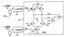
図1を参照すると、本発明のジッタ注入システムの実施態様を使用する同相モード論理(CML)回路の差動出力100の部分略図が示されている。高速送信機の場合、データは、一般に、ある点から別の点に差動出力形式で移動する。これらの差動出力は、金属酸化物半導体(MOS)、同相モード論理(CML)またはその他の種類の差動出力バッファから構成された差動トランジスタの対を使用して生成される。こうした差動出力の一例をボックス101で図1に示す。
Referring to FIG. 1, a partial schematic diagram of a
図1の基準信号電圧Vcsは、差動トランジスタの対102、すなわち、Q1(103)およびQ2(104)に提供される電流の量を決定する。これは、以下の公式で表すことができる:
The reference signal voltage Vcs of FIG. 1 determines the amount of current provided to the

ただし、Icsは、ドレインから電流吸込トランジスタQ3(105)のソースまで流れる電流である。電流吸込トランジスタQ3(105)は、Q1(103)およびQ2(104)により提供される電流を同期させる。βは、MOSトランジスタのゲイン係数であり;Vcsは、トランジスタQ3(105)のゲート電圧であり;Vtは、閾値電圧であり、Vdsは、電流吸込トランジスタQ3(105)のドレインソース電圧である。Icsが、式1により与えられ、かつ図3に示されているゲート電圧Vcsの関数であると仮定すると、Icsの値は、ゲート電圧Vcsの値を変更することにより制御することができる。
Here, Ics is a current flowing from the drain to the source of the current sink transistor Q3 (105). Current sink transistor Q3 (105) synchronizes the current provided by Q1 (103) and Q2 (104). β is the gain coefficient of the MOS transistor; Vcs is the gate voltage of the transistor Q3 (105); Vt is the threshold voltage; Vds is the drain-source voltage of the current sink transistor Q3 (105). Assuming that Ics is given by
トランジスタの差動対102、Q1(103)およびQ2(104)は、2つの入力、VinおよびVinbを有する。差動入力の構成の性質により、Vinが論理的にハイ(High)である場合、Vinbは、論理的にロー(Low)状態であると論理的に予測される。逆に、Vinbがハイである場合、Vinはローであると予測される。
Transistor
代表的なICの用途では、2つの差動出力、VoutおよびVoutbは、受信機のそれぞれの差動入力に接続される。各出力部VoutおよびVoutbからの負荷を含む受信機の入力負荷は、図1のコンデンサ110および111に示されている容量性負荷CLおよびCLbにより表すことができる。これらの負荷静電容量CLおよびCLbの両端間電圧は、以下により表される:
In a typical IC application, two differential outputs, Vout and Voutb, are connected to respective differential inputs of the receiver. The input load of the receiver including the load from each output Vout and Voutb can be represented by capacitive loads CL and CLb shown in
![]()
![]()
ただし、VoutおよびVoutbは、静電容量CLおよびCLbの両端間電圧である。 However, Vout and Voutb are voltages across the capacitances CL and CLb.
コンデンサCLおよびCLbをt秒間充電することができる場合、コンデンサCLおよびCLbにより蓄積される電荷は、以下により表される: If capacitors CL and CLb can be charged for t seconds, the charge accumulated by capacitors CL and CLb is represented by:
![]()
![]()
![]()
![]()
ただし、IおよびIbは、コンデンサCLおよびCLB中に流入する電流である。したがって、式2は、以下のように書き直すことができる: Here, I and Ib are currents flowing into the capacitors CL and CLB. Thus, Equation 2 can be rewritten as:
![]()
![]()
![]()
![]()
ただし、IおよびIbは、コンデンサCLおよびCLB中に流入する電流であり、tは、コンデンサCLおよびCLBをそれぞれの電圧VoutおよびVoutbまで充電するのに要する時間である。CLおよびCLbが定数であり、Voutの値が一定であると仮定すると、以下である: Where I and Ib are currents flowing into the capacitors CL and CLB, and t is the time required to charge the capacitors CL and CLB to the respective voltages Vout and Voutb. Assuming that CL and CLb are constants and the value of Vout is constant, then:
ただし、IおよびIbは、コンデンサCLおよびCLBをそれぞれ充電および放電する電流である。式6および式7は、予め決められたレベルまでコンデンサを充電するための時間つまり立上り時間、または、予め決められたレベルまでコンデンサを放電するための時間つまり立下り時間が電流IまたはIbに逆比例することを示す。 However, I and Ib are currents for charging and discharging the capacitors CL and CLB, respectively. Equations 6 and 7 show that the time to charge the capacitor to a predetermined level, that is, the rise time, or the time to discharge the capacitor to the predetermined level, that is, the fall time, is opposite to the current I or Ib. Indicates proportionality.
図1では、コンデンサCL(110)を充電するソース電流Iscは、能動負荷トランジスタQ5(116)により提供され、コンデンサCLb(111)を充電するソース電流Iscbは能動負荷トランジスタQ4(115)により提供される。一方、コンデンサCL(110)およびCLb(111)を放電する吸込電流Iskは、トランジスタQ3(105)により提供される。既存の送信機の動作のノーマルモードでは、基準電圧VcsおよびVcs2の値は、ソース電流および吸込電流を制御し、これらの電圧は十分に特性化され、一定に保たれる。 In FIG. 1, the source current Isc for charging the capacitor CL (110) is provided by the active load transistor Q5 (116), and the source current Iscb for charging the capacitor CLb (111) is provided by the active load transistor Q4 (115). The On the other hand, the sink current Isk for discharging the capacitors CL (110) and CLb (111) is provided by the transistor Q3 (105). In the normal mode of operation of existing transmitters, the values of the reference voltages Vcs and Vcs2 control the source and sink currents, and these voltages are well characterized and kept constant.
電圧Vcs2は、飽和領域で作動可能であるように電流源Q4(115)およびQ5(116)に印加される場合、式1により示される負荷コンデンサCL(110)CLb(111)のほかにQ1(103)およびQ2(104)に電流を提供する。したがって、VinがVinbと比較して高い場合、トランジスタQ1(104)は、飽和領域でも動作し、その結果、電流はQ4(115)からQ1(103)を通ってQ3(105)に流れる。さらに、トランジスタQ1は飽和領域で動作するので、負荷コンデンサCLb(111)も放電する。このモードでは、Vinbは低いので、トランジスタQ2は非活動状態であり、その結果、Q2(114)からQ3(105)に至る電流の流れは存在しない。この場合、Q5(116)からの電流は、負荷コンデンサCL(110)を充電するためにのみ使用される。
When the voltage Vcs2 is applied to the current sources Q4 (115) and Q5 (116) so as to be operable in the saturation region, in addition to the load capacitor CL (110) CLb (111) shown by
上記のようにコンデンサを充電および放電するために要する時間の量は、式6および式7により支配される。本発明によると、Voutは一定であり、コンデンサCL(110)およびCLb(111)のサイズは一定である。したがって、充電コンデンサCLまたはCLbの充電に要する時間は、電流に逆比例する。したがって、この関係は、本発明によるジッタを提供するために使用することができる。電流の量を変更することにより、信号がVinからVoutb、またはVinbからVoutに達する時間を制御することができる。電流が大きければ大きいほど、所要時間は減少し、電流が小さければ小さいほど、所要時間は増加する。したがって、電圧源Vcsの出力電圧が増加し、その結果、電流吸込トランジスタQ3(105)を貫流する電流Iskの量を増加させる。この関係、つまり電流吸込Iskおよび電圧Vcsは、上記の式1により支配される。したがって、Vcsが増加すると、Iskの値も増加する。式4および式5は、コンデンサCLまたはCLbを放電する時間が、電流、この場合はIskに逆比例することを示す。Iskの値が大きくなれば、コンデンサCLまたはCLbを放電する時間量は小さくなる。この場合、出力部におけるハイからローへの遷移は、早く発生したように見えるであろう。逆に、電圧Vcsの値が減少すると、Iskの値は小さくなる。したがって、負荷コンデンサCLまたはCLbを放電する時間は長くなる。この場合、出力部におけるハイからローへの遷移は、遅く発生したように見えるであろう。これを図3に示す。
The amount of time required to charge and discharge the capacitor as described above is governed by Equation 6 and Equation 7. According to the present invention, Vout is constant and the sizes of capacitors CL (110) and CLb (111) are constant. Therefore, the time required for charging the charging capacitor CL or CLb is inversely proportional to the current. This relationship can therefore be used to provide jitter according to the present invention. By changing the amount of current, the time for the signal to reach from Vin to Voutb or from Vinb to Vout can be controlled. The larger the current, the shorter the required time, and the smaller the current, the longer the required time. Therefore, the output voltage of the voltage source Vcs increases, and as a result, the amount of current Isk flowing through the current sink transistor Q3 (105) is increased. This relationship, that is, current sink Isk and voltage Vcs is governed by
図3は、基準電圧Vcs2の値を変えることにより、出力信号Voutの立上りエッジの到着時間をどのように変更することができるかをグラフで示す。同様に、出力信号Voutの立下りエッジの到着時間は、Vcsの値を変えることにより変化させることができる。図3では、x軸は信号の到着時間を示し、y軸は、出力ポートVoutからの出力電流を表す。 FIG. 3 is a graph showing how the arrival time of the rising edge of the output signal Vout can be changed by changing the value of the reference voltage Vcs2. Similarly, the arrival time of the falling edge of the output signal Vout can be changed by changing the value of Vcs. In FIG. 3, the x-axis represents the arrival time of the signal, and the y-axis represents the output current from the output port Vout.
電圧源Vcsは、上記のように出力信号の立下り時間を制御し、電圧源Vcs2は出力信号の立上り時間を制御する。電圧源Vcs2は、ソース電流Iscを提供してコンデンサCLを充電し、および、Iscbを提供してコンデンサCLbを充電する。IscおよびIscbのVcs2に対する関係は、式1により支配される。式1は、電圧Vcs2が増加すると、ソース電流IscおよびIscbが増加することを示す。式4は、IscおよびIscbが大きい場合、コンデンサCLまたはCLbを充電する時間がより小さいことを示す。この場合、出力信号は、より速い速度で低から高へ遷移する。ロー出力からハイ出力の信号は、より早い時間で出力部に出現したように見えるであろう。一方、電圧Vcs2が減少すると、式1は、ソース電流IscおよびIscbが減少することを示す。式4は、IscおよびIscbが小さい場合、コンデンサCLまたはCLbを充電するために、より長時間を要することを示す。したがって、低出力から高出力の信号は、より遅い時間で出力部に出現したように見えるであろう。
The voltage source Vcs controls the fall time of the output signal as described above, and the voltage source Vcs2 controls the rise time of the output signal. The voltage source Vcs2 provides the source current Isc to charge the capacitor CL, and provides the Iscb to charge the capacitor CLb. The relationship of Isc and Iscb to Vcs2 is governed by
したがって、本発明の実施態様によると、試験モードでは、出力電圧(VoutおよびVoutb)の立上り時間および立下り時間は、吸込およびソース基準電圧VcsおよびVcs2の値を変調することにより変えることができる。出力電圧の立上り時間および立下り時間におけるこの変化の影響は、差動出力101により送信されるデータストリーム中へのジッタの注入である。この変調は、変調器120および121を使用して行われ、それぞれ電圧発生器130および131の出力を変調する。
Thus, according to an embodiment of the present invention, in the test mode, the rise and fall times of the output voltages (Vout and Voutb) can be varied by modulating the values of the suction and source reference voltages Vcs and Vcs2. The effect of this change in output voltage rise and fall times is the injection of jitter into the data stream transmitted by the
Vcs発生器130およびVcs2発生器131は、適切な電圧VcsをトランジスタQ3(105)に、電圧Vcs2をQ4(115)およびQ5(116)に提供するトランジスタの集合から構成される。発生器130を制御または変調することにより、Q3(105)に提供される電圧Vcsの量を制御または変調することができる。同様に、Vcs2発生器131は、Q4(115)およびQ5(116)におけるVcs2電圧を変化させるように変調することができる。発生器におけるこうした変調は、ジッタの導入に使用することができる。変調器は、電圧波源発生波形、たとえばサイン波、三角波、擬似ランダム2進シーケンス(PRBS)、またはその他のランダム信号の形態を取ることができる。
本発明の実施態様を使用する差動出力バッファでは、能動負荷トランジスタQ4(115)およびQ5(116)は、抵抗器などの受動負荷と置き換えることができる。この場合、出力信号の立上り時間は、外部で制御することはできない。しかし、出力信号の立下り時間は、Vcsを変調してジッタを導入することにより、制御することができる。 In a differential output buffer using embodiments of the present invention, active load transistors Q4 (115) and Q5 (116) can be replaced with passive loads such as resistors. In this case, the rise time of the output signal cannot be controlled externally. However, the fall time of the output signal can be controlled by modulating Vcs and introducing jitter.
高速送信機201とともに動作し、高速データストリームに使用されるジッタ注入および測定回路200の実施態様を図2に示す。新世代のネットワークプロセス、インターネット・アプリケーション、ファイバチャネル・アプリケーションなどは、1個のチップ内に多くの送信機および受信機を使用する。この実施態様の場合、自動試験機器(ATE)202は、所望の種類のジッタに応じた変調信号をVcs発生器130およびVcs2発生器131に送信する。あるいは、組み込み自己試験(BIST)回路をATE202モジュールと置き換えるか、またはBISTおよびATEの組合せを使用することができる。ジッタの量は、オンチップ時間間隔分析器(TIA)モジュール203により測定するか、またはその他のタイプのジッタ測定技術、モジュールまたは装置により測定することができる。ジッタ測定結果は、ライン204を介してATE202にフィードバックすることが好ましい。
An embodiment of a jitter injection and
詳細には、図2は、VcsおよびVcs2変調信号を使用して、多重CML出力バッファ205(1〜n)に接続されたVcs発生器130およびVcs2発生器131を変調する方法を略図で示す。発生器130および131は、各送信機210(1)〜210(n)のバッファにジッタを同時に提供する。したがって、発生器の集合を制御することにより、数個の送信機を変調することができる。したがって、CMLバッファ205(1〜n)は、出力データストリームTx−VoutまたはTx−Voutb中にジッタを導入するように変調される。出力データストリームは、受信機202内に方向付けられる。好ましくは、受信機206の前面にある時間間隔分析器(TIA)203は、ジッタの量を測定する。TIA203は、受信機206でのジッタの値をに返し、ATE202は、その値を使用して変調を制御する。ATE201は、変調信号をVcsおよびVcs2発生器130および131に提供する。各送信機は、変調を同時に調節する。しかし、本発明の実施態様は、1個または数個の送信機を本発明により変調することを可能にする。
Specifically, FIG. 2 schematically illustrates a method for modulating
図2は、送信機210(1)〜210(n)の最終出力段階において注入されるジッタを示す。しかし、ジッタは、必ずしも最終出力段階においてのみ注入する必要はない。用途に応じて、ジッタは、1個以上の適切な中間差動バッファの立上り時間および立下り時間を本発明に従って変調することにより、データおよび/またはクロック経路内のどこにでも選択的に注入することができる。 FIG. 2 shows the jitter injected at the final output stage of transmitters 210 (1) -210 (n). However, jitter need not necessarily be injected only at the final output stage. Depending on the application, jitter can be selectively injected anywhere in the data and / or clock path by modulating the rise and fall times of one or more suitable intermediate differential buffers according to the present invention. Can do.
本発明によるジッタ試験機構を提供するには、最低量のハードウェアがチップ上に必要である。本発明は、送信機の出力部に組み込むことができ、すべての変調電圧は、ATE202により提供される。あるいは、最低の諸経費は、データビットストリーム中にテストジッタを注入するための本発明のシステムおよび方法を組み込むチップに関して必要である。CMLバッファは、一般に、高速送信機または送受信機を使用する殆どのチップの場合、既に送信機の出力バッファの一部である。外部ATEの制御は、ATEが本発明により変調信号を送信することを可能にする。 In order to provide a jitter test mechanism according to the present invention, a minimal amount of hardware is required on the chip. The present invention can be incorporated into the output of the transmitter and all modulation voltages are provided by the ATE 202. Alternatively, the lowest overhead is necessary for a chip incorporating the system and method of the present invention for injecting test jitter into the data bitstream. The CML buffer is generally already part of the output buffer of the transmitter for most chips that use high-speed transmitters or transceivers. Control of the external ATE enables the ATE to transmit a modulated signal according to the present invention.
図4を参照すると、本発明の実施態様によりジッタをデータビットストリーム中に注入するための方法400がフローチャートで示されている。401では、第1電圧発生器は、第1制御電圧を変調して、出力信号の立上り時間を制御する。ボックス402では、第2電圧発生器は、第2制御電圧を変調して、出力信号の立下り時間を制御する。差動対は、一対の入力電圧を受信する。ボックス403を参照。電流吸込装置は、ボックス404で、1個の発生器により提供される制御電圧を使用して作動し、差動対が受信する入力電圧に応じて出力電圧を提供する。405では、電流源は、差動対が受信する入力電圧に応じて、1個の発生器が提供する基準電圧を使用して出力信号を提供する。したがって、ジッタは、ボックス406に詳細に記載するように、出力信号中に提供される。特に、出力信号および入力電圧の立上り時間および立下り時間の同時の変動は、電流吸込および電流源により出力される出力信号およびジッタを決定する。
Referring to FIG. 4, a flowchart illustrates a
本発明およびその利点について詳細に説明してきたが、様々な変更、置き換えおよび修正は、添付の請求の範囲に定義する本発明の精神および範囲から逸脱することなく、本明細書に加えることができることが分かるはずである。さらに、本発明の範囲は、本明細書に記載したプロセス、機械、製法、物質の組成、手段、方法およびステップの特定の実施態様に制限することを意図するものではない。当業者は、本発明の開示により、現在既存するか、または後に開発され、本明細書に記載した対応する実施態様と実質的に同じ機能を果たすか、または同じ結果を実質的に達成するプロセス、機械、製法、物質の組成、手段、方法またはステップは、本発明に従って使用できることを容易に理解するであろう。したがって、添付の請求の範囲は、こうしたプロセス、機械、製法、物質の組成、手段、方法またはステップを本発明の範囲に含むことを意図している。念のため、以下に本発明の実施態様を列挙する。 Although the invention and its advantages have been described in detail, various changes, substitutions and modifications can be made herein without departing from the spirit and scope of the invention as defined in the appended claims. Should be understood. Furthermore, the scope of the present invention is not intended to be limited to the specific embodiments of the processes, machines, processes, material compositions, means, methods and steps described herein. One skilled in the art, in accordance with the disclosure of the present invention, will now have a process that performs substantially the same function or substantially achieves the same results as the corresponding embodiments described or later developed and described herein. It will be readily understood that any machine, process, composition of matter, means, method or step may be used in accordance with the present invention. Accordingly, the appended claims are intended to include within their scope such processes, machines, manufacture, compositions of matter, means, methods, or steps. As a precaution, the embodiments of the present invention are listed below.
(実施態様1)
テストジッタをデータビットストリーム中に注入するための方法(400)であって、
第1電圧発生器を変調して、出力信号の立上り時間を制御するステップ(401)と、
第2電圧発生器を変調して、前記出力信号の立下り時間を制御するステップ(402)と、
一対の入力電圧を差動対により受信するステップ(403)と、
少なくとも1個の前記電圧発生器により提供される第1制御電圧で、少なくとも1個の電流吸込装置を作動させて、前記差動対により受信される前記入力電圧に応じて出力電圧を提供するステップ(404)と、
複数の電流源を作動させ、前記差動対が受信した前記入力電圧に応じて、前記1個の電圧発生器が提供する基準電圧を使用して、前記出力信号を提供するステップ(405)で、前記入力電圧と同時の立上り時間および立下り時間の同時の変動(406)が、前記電流吸込装置および前記電流源により出力される前記出力信号及びジッタを決定するステップと
を有する方法。
(Embodiment 1)
A method (400) for injecting test jitter into a data bitstream comprising:
Modulating the first voltage generator to control the rise time of the output signal (401);
Modulating the second voltage generator to control the fall time of the output signal (402);
Receiving a pair of input voltages by a differential pair (403);
Activating at least one current sink with a first control voltage provided by at least one of the voltage generators to provide an output voltage in response to the input voltage received by the differential pair. (404)
Activating a plurality of current sources and providing the output signal using a reference voltage provided by the one voltage generator in response to the input voltage received by the differential pair (405). And a simultaneous variation (406) in rise time and fall time coincident with the input voltage determines the output signal and jitter output by the current sink and the current source.
(実施態様2)
前記ジッタの特性が、第1電圧発生器の前記変調、および第2電圧発生器の前記変調により決定される、実施態様1に記載の方法。
(Embodiment 2)
2. The method of
(実施態様3)
前記特性が、少なくとも部分的に前記ジッタの周波数を含む、実施態様2に記載の方法。
(Embodiment 3)
3. The method of embodiment 2, wherein the characteristic includes at least partially the frequency of the jitter.
(実施態様4)
前記特性が、少なくとも部分的に前記ジッタの振幅を含む、実施態様2または3に記載の方法。
(Embodiment 4)
4. The method of embodiment 2 or 3, wherein the characteristic includes at least partially the amplitude of the jitter.
(実施態様5)
前記特性が、少なくとも部分的に前記ジッタの種類を含む、実施態様2に記載の方法。
(Embodiment 5)
3. The method of embodiment 2, wherein the characteristic includes at least partially the jitter type.
(実施態様6)
前記ジッタの前記種類が、
帯域内ジッタと;
帯域外ジッタと;
正弦波形ジッタと;
パターン依存ジッタと;
位相依存ジッタと;
干渉依存ジッタと
から成るジッタの種類の群から選択した少なくとも1種類である、実施態様5に記載の方法。
(Embodiment 6)
The type of jitter is
With in-band jitter;
With out-of-band jitter;
With sinusoidal jitter;
With pattern dependent jitter;
Phase-dependent jitter;
6. The method of embodiment 5, wherein the method is at least one selected from the group of jitter types consisting of interference dependent jitter.
(実施態様7)
前記変調が、外部自動試験機器回路により行われる、実施態様1に記載の方法。
(Embodiment 7)
2. The method of
(実施態様8)
前記変調が、内蔵自己試験回路により行われる、実施態様1、2または3に記載の方法。
(Embodiment 8)
Embodiment 4. The method of
(実施態様9)
テストジッタを1つ以上の独立するデータビットストリーム中に注入するシステム(100)であって、
少なくとも1個の変調器(120、121)と;
複数のデータビットストリーム発生器(130、131)で、前記発生器の各々が少なくとも1個の前記変調器により変調される発生器と;
差動対(102)であって、前記差動対の第1出力が第1入力電圧により制御され、前記差動対の第2出力が第2入力電圧により制御される差動対と;
各データビットストリームのための電流吸込装置(105)であって、前記電流吸込装置が、前記第1電圧発生器により提供される第1制御電圧により作動され、各電流吸込装置が、前記差動対に提供される前記入力電圧に応じて出力電圧を提供する電流吸込装置と;
前記第2電圧発生器により提供される第2制御電圧により制御される複数の電流源装置であって、前記各電流源が、前記差動対に提供される前記入力電圧に応じて出力電圧を提供し、各電流源および各電流吸込装置が前記差動対に提供される前記入力電圧に応じて出力電圧を提供し、前記入力電圧に関連する前記第1および第2制御電圧の同時の変動が、出力信号およびジッタを決定する電流源装置と
を含むシステム。
(Embodiment 9)
A system (100) for injecting test jitter into one or more independent data bitstreams,
At least one modulator (120, 121);
A plurality of data bitstream generators (130, 131), each of said generators being modulated by at least one said modulator;
A differential pair (102), wherein a first output of the differential pair is controlled by a first input voltage, and a second output of the differential pair is controlled by a second input voltage;
A current sink for each data bitstream (105), wherein said current sink is activated by a first control voltage provided by said first voltage generator, and each current sink is said differential A current sink that provides an output voltage in response to the input voltage provided to a pair;
A plurality of current source devices controlled by a second control voltage provided by the second voltage generator, wherein each current source outputs an output voltage according to the input voltage provided to the differential pair; Each current source and each current sink provides an output voltage in response to the input voltage provided to the differential pair, and a simultaneous variation of the first and second control voltages associated with the input voltage A current source device that determines the output signal and jitter.
(実施態様10)
テストジッタを1つ以上の独立するデータビットストリーム中に注入するように構成された回路(200)であって、
少なくとも1個の変調器(202)と;
複数のデータビットストリーム発生器(130、131)で、前記発生器の各々が、少なくとも1個の前記変調器により変調される発生器と;
送信機の出力バッファ(205)とを備え、
前記出力バッファは、
差動対であって、前記差動対の第1出力が第1入力電圧により制御され、前記差動対の第2出力が第2入力電圧により制御される差動対と;
各データビットストリームのための電流吸込装置であって、前記電流吸込装置が、前記第1電圧発生器により提供される第1制御電圧により作動され、各電流吸込装置が、前記差動対に提供される前記入力電圧に応じて出力電圧を提供する電流吸込装置と;
各々が前記出力電圧の1つを受信、記憶および放電する複数の負荷コンデンサと;
前記第2電圧発生器により提供される第2制御電圧により制御される複数の電流源装置であって、前記各電流源が、前記差動対に提供される前記入力電圧に応じて出力電圧を提供し、各電流源および各電流吸込装置が、前記差動対に提供される前記入力電圧に応じて出力電圧を提供し、前記入力電圧に関連する前記第1および第2制御電圧の同時の変動が、出力信号およびジッタを決定する電流源装置と
を含む送信機の出力バッファ(205)と;
を具備することを特徴とする回路。
(Embodiment 10)
A circuit (200) configured to inject test jitter into one or more independent data bitstreams;
At least one modulator (202);
A plurality of data bitstream generators (130, 131), each of said generators being modulated by at least one said modulator;
An output buffer (205) of the transmitter,
The output buffer is
A differential pair, wherein a first output of the differential pair is controlled by a first input voltage, and a second output of the differential pair is controlled by a second input voltage;
A current sink for each data bitstream, wherein the current sink is activated by a first control voltage provided by the first voltage generator, and each current sink is provided to the differential pair A current sink that provides an output voltage in response to the input voltage being applied;
A plurality of load capacitors each receiving, storing and discharging one of said output voltages;
A plurality of current source devices controlled by a second control voltage provided by the second voltage generator, wherein each current source outputs an output voltage according to the input voltage provided to the differential pair; Each current source and each current sink provides an output voltage in response to the input voltage provided to the differential pair, and the first and second control voltages associated with the input voltage are simultaneously An output buffer (205) of the transmitter including a current source device whose variation determines the output signal and jitter;
A circuit comprising:
Claims (5)
個々に制御電圧を生成するよう動作する複数の変調電圧発生器と、
前記複数の変調電圧発生器のうちの第一の変調電圧発生器により供給される第一の制御電圧を受信するように接続される電流吸込装置と、
前記複数の変調電圧発生器のうちの第二の変調電圧発生器により供給される第二の制御電圧を受信するように接続される複数の電流源装置と、
各前記電流源装置からの電流を受信し前記電流吸込装置へ供給するように接続され、差動入力電圧に応答して差動出力電圧を生成するよう動作する差動対とを備え、
前記第一の制御電圧に応じた前記電流吸込装置による電流吸込が前記差動出力電圧の下降時間を定義し、
前記第二の制御電圧に応じて前記電流源装置により供給される電流が前記差動出力電圧の上昇時間を定義し、
前記差動入力電圧に同期した、前記第一および第二の制御電圧の変調が、前記差動出力電圧にジッタを重畳することを特徴とするシステム。 A system for injecting test jitter into a data bitstream,
A plurality of modulation voltage generators that individually operate to generate a control voltage;
A current sink device connected to receive the first control voltage supplied by the first modulation voltage generator of the plurality of modulation voltage generator,
A plurality of current source devices connected to receive a second control voltage supplied by a second modulation voltage generator of the plurality of modulation voltage generators;
A differential pair connected to receive and supply current from each of the current source devices to the current sink device, and to operate to generate a differential output voltage in response to a differential input voltage;
Current sinking by the current sinking device according to the first control voltage defines a fall time of the differential output voltage;
A current supplied by the current source device in response to the second control voltage defines a rise time of the differential output voltage;
The synchronized to the differential input voltage, system modulation of the first and second control voltages, characterized by superimposing jitter in the differential output voltage.
Applications Claiming Priority (1)
| Application Number | Priority Date | Filing Date | Title |
|---|---|---|---|
| US10/360,159 US7184469B2 (en) | 2003-02-06 | 2003-02-06 | Systems and methods for injection of test jitter in data bit-streams |
Publications (3)
| Publication Number | Publication Date |
|---|---|
| JP2004242304A JP2004242304A (en) | 2004-08-26 |
| JP2004242304A5 JP2004242304A5 (en) | 2007-04-05 |
| JP4410574B2 true JP4410574B2 (en) | 2010-02-03 |
Family
ID=32771369
Family Applications (1)
| Application Number | Title | Priority Date | Filing Date |
|---|---|---|---|
| JP2004025173A Expired - Lifetime JP4410574B2 (en) | 2003-02-06 | 2004-02-02 | System and method for injecting test jitter into a data bitstream |
Country Status (3)
| Country | Link |
|---|---|
| US (1) | US7184469B2 (en) |
| JP (1) | JP4410574B2 (en) |
| DE (1) | DE10348327B4 (en) |
Families Citing this family (7)
| Publication number | Priority date | Publication date | Assignee | Title |
|---|---|---|---|---|
| US7315574B2 (en) * | 2004-05-03 | 2008-01-01 | Dft Microsystems, Inc. | System and method for generating a jittered test signal |
| US7480329B2 (en) * | 2004-10-29 | 2009-01-20 | Agilent Technologies, Inc. | Method of finding data dependent timing and voltage jitter for different bits in an arbitrary digital signal in accordance with selected surrounding bits |
| US7369605B2 (en) * | 2004-12-15 | 2008-05-06 | Spirent Communications | Method and device for injecting a differential current noise signal into a paired wire communication link |
| JP4806679B2 (en) | 2005-06-01 | 2011-11-02 | 株式会社アドバンテスト | Jitter generation circuit |
| JP4384207B2 (en) * | 2007-06-29 | 2009-12-16 | 株式会社東芝 | Semiconductor integrated circuit |
| US8179952B2 (en) * | 2008-05-23 | 2012-05-15 | Integrated Device Technology Inc. | Programmable duty cycle distortion generation circuit |
| US8194721B2 (en) * | 2008-05-23 | 2012-06-05 | Integrated Device Technology, Inc | Signal amplitude distortion within an integrated circuit |
Family Cites Families (6)
| Publication number | Priority date | Publication date | Assignee | Title |
|---|---|---|---|---|
| US3325730A (en) * | 1963-12-23 | 1967-06-13 | Hughes Aircraft Co | Pulse time jitter measuring system |
| US3937945A (en) * | 1974-06-25 | 1976-02-10 | The United States Of America As Represented By The United States National Aeronautics And Space Administration Office Of General Counsel-Code Gp | Apparatus for simulating optical transmission links |
| US6466072B1 (en) * | 1998-03-30 | 2002-10-15 | Cypress Semiconductor Corp. | Integrated circuitry for display generation |
| EP1162739B1 (en) | 2001-04-03 | 2003-03-05 | Agilent Technologies, Inc. (a Delaware corporation) | Filter injecting data dependent jitter and level noise |
| US6847232B2 (en) * | 2001-11-08 | 2005-01-25 | Texas Instruments Incorporated | Interchangeable CML/LVDS data transmission circuit |
| US6958640B2 (en) * | 2003-12-31 | 2005-10-25 | Intel Corporation | Interpolation delay cell for 2ps resolution jitter injector in optical link transceiver |
-
2003
- 2003-02-06 US US10/360,159 patent/US7184469B2/en active Active
- 2003-10-17 DE DE10348327A patent/DE10348327B4/en not_active Expired - Fee Related
-
2004
- 2004-02-02 JP JP2004025173A patent/JP4410574B2/en not_active Expired - Lifetime
Also Published As
| Publication number | Publication date |
|---|---|
| US20040156429A1 (en) | 2004-08-12 |
| DE10348327B4 (en) | 2009-06-25 |
| DE10348327A1 (en) | 2004-08-26 |
| US7184469B2 (en) | 2007-02-27 |
| JP2004242304A (en) | 2004-08-26 |
Similar Documents
| Publication | Publication Date | Title |
|---|---|---|
| US7979754B2 (en) | Voltage margin testing for proximity communication | |
| KR101392102B1 (en) | Compensation techniques for reducing power consumption in digital circuitry | |
| US7142005B1 (en) | Method and apparatus for a reference clock buffer system | |
| JP4410574B2 (en) | System and method for injecting test jitter into a data bitstream | |
| JP2007523507A (en) | Timing generator and method with bias current compensation circuit | |
| US20100164531A1 (en) | Tunable stress technique for reliability degradation measurement | |
| US9209809B1 (en) | Circuits for and methods of controlling output swing in a current-mode logic circuit | |
| US6278312B1 (en) | Method and apparatus for generating a reference voltage signal derived from complementary signals | |
| KR20090045499A (en) | Semiconductor device with controllable decoupling capacitor | |
| CN110476071B (en) | Photodiode emulator, test circuit and method for emulating a photodiode | |
| US7355467B2 (en) | Physical layers | |
| US6104254A (en) | VCO in CMOS technology having an operating frequency of 1 GHz and greater | |
| Kim et al. | A 20-Gb/s 256-Mb DRAM with an inductorless quadrature PLL and a cascaded pre-emphasis transmitter | |
| US7123075B2 (en) | Current mirror compensation using channel length modulation | |
| JP2007033386A (en) | Timing generator and semi-conductor testing equipment | |
| US7915932B2 (en) | Semiconductor integrated circuit | |
| KR20210146451A (en) | parallel path delay line | |
| US20160065214A1 (en) | Semiconductor device | |
| Heydari et al. | A 40-GHz flip-flop-based frequency divider | |
| JPH04208563A (en) | Method and apparatus for compensation of inherent unevenness of electric characteristic at field-effect transistor in integrated circuit among plurality of integrated circuits. | |
| US11003204B1 (en) | Relaxation oscillator having a dynamically controllable current source | |
| Kim et al. | A 10-Gb/s 6-V pp differential modulator driver in 65-nm CMOS | |
| US7064600B1 (en) | Limit swing charge pump and method thereof | |
| US20100327915A1 (en) | Semiconductor device and method for resetting the same | |
| US7212060B1 (en) | Ground bounce protection circuit for a test mode pin |
Legal Events
| Date | Code | Title | Description |
|---|---|---|---|
| A521 | Request for written amendment filed |
Free format text: JAPANESE INTERMEDIATE CODE: A523 Effective date: 20070125 |
|
| A621 | Written request for application examination |
Free format text: JAPANESE INTERMEDIATE CODE: A621 Effective date: 20070125 |
|
| A711 | Notification of change in applicant |
Free format text: JAPANESE INTERMEDIATE CODE: A711 Effective date: 20070125 |
|
| A521 | Request for written amendment filed |
Free format text: JAPANESE INTERMEDIATE CODE: A821 Effective date: 20070125 |
|
| A977 | Report on retrieval |
Free format text: JAPANESE INTERMEDIATE CODE: A971007 Effective date: 20090626 |
|
| A131 | Notification of reasons for refusal |
Free format text: JAPANESE INTERMEDIATE CODE: A131 Effective date: 20090707 |
|
| A521 | Request for written amendment filed |
Free format text: JAPANESE INTERMEDIATE CODE: A523 Effective date: 20090928 |
|
| TRDD | Decision of grant or rejection written | ||
| A01 | Written decision to grant a patent or to grant a registration (utility model) |
Free format text: JAPANESE INTERMEDIATE CODE: A01 Effective date: 20091110 |
|
| A01 | Written decision to grant a patent or to grant a registration (utility model) |
Free format text: JAPANESE INTERMEDIATE CODE: A01 |
|
| A61 | First payment of annual fees (during grant procedure) |
Free format text: JAPANESE INTERMEDIATE CODE: A61 Effective date: 20091113 |
|
| R150 | Certificate of patent or registration of utility model |
Ref document number: 4410574 Country of ref document: JP Free format text: JAPANESE INTERMEDIATE CODE: R150 |
|
| FPAY | Renewal fee payment (event date is renewal date of database) |
Free format text: PAYMENT UNTIL: 20121120 Year of fee payment: 3 |
|
| FPAY | Renewal fee payment (event date is renewal date of database) |
Free format text: PAYMENT UNTIL: 20121120 Year of fee payment: 3 |
|
| S111 | Request for change of ownership or part of ownership |
Free format text: JAPANESE INTERMEDIATE CODE: R313113 |
|
| S531 | Written request for registration of change of domicile |
Free format text: JAPANESE INTERMEDIATE CODE: R313531 |
|
| FPAY | Renewal fee payment (event date is renewal date of database) |
Free format text: PAYMENT UNTIL: 20121120 Year of fee payment: 3 |
|
| R360 | Written notification for declining of transfer of rights |
Free format text: JAPANESE INTERMEDIATE CODE: R360 |
|
| FPAY | Renewal fee payment (event date is renewal date of database) |
Free format text: PAYMENT UNTIL: 20121120 Year of fee payment: 3 |
|
| R370 | Written measure of declining of transfer procedure |
Free format text: JAPANESE INTERMEDIATE CODE: R370 |
|
| FPAY | Renewal fee payment (event date is renewal date of database) |
Free format text: PAYMENT UNTIL: 20121120 Year of fee payment: 3 |
|
| S111 | Request for change of ownership or part of ownership |
Free format text: JAPANESE INTERMEDIATE CODE: R313113 |
|
| S531 | Written request for registration of change of domicile |
Free format text: JAPANESE INTERMEDIATE CODE: R313531 |
|
| FPAY | Renewal fee payment (event date is renewal date of database) |
Free format text: PAYMENT UNTIL: 20121120 Year of fee payment: 3 |
|
| R350 | Written notification of registration of transfer |
Free format text: JAPANESE INTERMEDIATE CODE: R350 |
|
| FPAY | Renewal fee payment (event date is renewal date of database) |
Free format text: PAYMENT UNTIL: 20121120 Year of fee payment: 3 |
|
| FPAY | Renewal fee payment (event date is renewal date of database) |
Free format text: PAYMENT UNTIL: 20131120 Year of fee payment: 4 |
|
| R250 | Receipt of annual fees |
Free format text: JAPANESE INTERMEDIATE CODE: R250 |
|
| R250 | Receipt of annual fees |
Free format text: JAPANESE INTERMEDIATE CODE: R250 |
|
| R250 | Receipt of annual fees |
Free format text: JAPANESE INTERMEDIATE CODE: R250 |
|
| S111 | Request for change of ownership or part of ownership |
Free format text: JAPANESE INTERMEDIATE CODE: R313113 |
|
| S531 | Written request for registration of change of domicile |
Free format text: JAPANESE INTERMEDIATE CODE: R313531 |
|
| R350 | Written notification of registration of transfer |
Free format text: JAPANESE INTERMEDIATE CODE: R350 |
|
| R250 | Receipt of annual fees |
Free format text: JAPANESE INTERMEDIATE CODE: R250 |
|
| R250 | Receipt of annual fees |
Free format text: JAPANESE INTERMEDIATE CODE: R250 |
|
| R250 | Receipt of annual fees |
Free format text: JAPANESE INTERMEDIATE CODE: R250 |
|
| R250 | Receipt of annual fees |
Free format text: JAPANESE INTERMEDIATE CODE: R250 |
|
| R250 | Receipt of annual fees |
Free format text: JAPANESE INTERMEDIATE CODE: R250 |
|
| R250 | Receipt of annual fees |
Free format text: JAPANESE INTERMEDIATE CODE: R250 |
|
| R250 | Receipt of annual fees |
Free format text: JAPANESE INTERMEDIATE CODE: R250 |
|
| R250 | Receipt of annual fees |
Free format text: JAPANESE INTERMEDIATE CODE: R250 |
|
| R250 | Receipt of annual fees |
Free format text: JAPANESE INTERMEDIATE CODE: R250 |
|
| EXPY | Cancellation because of completion of term |