JP4410457B2 - Image forming technology using optical MEMS device - Google Patents
Image forming technology using optical MEMS device Download PDFInfo
- Publication number
- JP4410457B2 JP4410457B2 JP2002188861A JP2002188861A JP4410457B2 JP 4410457 B2 JP4410457 B2 JP 4410457B2 JP 2002188861 A JP2002188861 A JP 2002188861A JP 2002188861 A JP2002188861 A JP 2002188861A JP 4410457 B2 JP4410457 B2 JP 4410457B2
- Authority
- JP
- Japan
- Prior art keywords
- mems device
- micro
- image
- optical
- virtual
- Prior art date
- Legal status (The legal status is an assumption and is not a legal conclusion. Google has not performed a legal analysis and makes no representation as to the accuracy of the status listed.)
- Expired - Lifetime
Links
- 230000003287 optical effect Effects 0.000 title claims description 136
- 238000005516 engineering process Methods 0.000 title description 5
- 238000003384 imaging method Methods 0.000 claims description 91
- 238000000034 method Methods 0.000 claims description 4
- 230000008569 process Effects 0.000 claims description 2
- 239000000835 fiber Substances 0.000 description 109
- 230000006870 function Effects 0.000 description 45
- 238000005452 bending Methods 0.000 description 12
- 238000003491 array Methods 0.000 description 4
- 230000008859 change Effects 0.000 description 4
- 238000010586 diagram Methods 0.000 description 4
- 238000013507 mapping Methods 0.000 description 4
- 239000013307 optical fiber Substances 0.000 description 3
- 230000015572 biosynthetic process Effects 0.000 description 2
- 238000004519 manufacturing process Methods 0.000 description 2
- 230000015654 memory Effects 0.000 description 2
- 238000000926 separation method Methods 0.000 description 2
- 230000000153 supplemental effect Effects 0.000 description 2
- 230000009471 action Effects 0.000 description 1
- 239000002131 composite material Substances 0.000 description 1
- 230000000694 effects Effects 0.000 description 1
- 230000003993 interaction Effects 0.000 description 1
- 238000012544 monitoring process Methods 0.000 description 1
- 230000005855 radiation Effects 0.000 description 1
- 239000000758 substrate Substances 0.000 description 1
- 239000013589 supplement Substances 0.000 description 1
- 230000007704 transition Effects 0.000 description 1
- 238000001429 visible spectrum Methods 0.000 description 1
Images


Classifications
-
- G—PHYSICS
- G02—OPTICS
- G02B—OPTICAL ELEMENTS, SYSTEMS OR APPARATUS
- G02B6/00—Light guides; Structural details of arrangements comprising light guides and other optical elements, e.g. couplings
- G02B6/24—Coupling light guides
- G02B6/26—Optical coupling means
- G02B6/35—Optical coupling means having switching means
- G02B6/3564—Mechanical details of the actuation mechanism associated with the moving element or mounting mechanism details
- G02B6/3582—Housing means or package or arranging details of the switching elements, e.g. for thermal isolation
-
- G—PHYSICS
- G02—OPTICS
- G02B—OPTICAL ELEMENTS, SYSTEMS OR APPARATUS
- G02B26/00—Optical devices or arrangements for the control of light using movable or deformable optical elements
- G02B26/08—Optical devices or arrangements for the control of light using movable or deformable optical elements for controlling the direction of light
- G02B26/0816—Optical devices or arrangements for the control of light using movable or deformable optical elements for controlling the direction of light by means of one or more reflecting elements
- G02B26/0833—Optical devices or arrangements for the control of light using movable or deformable optical elements for controlling the direction of light by means of one or more reflecting elements the reflecting element being a micromechanical device, e.g. a MEMS mirror, DMD
- G02B26/0841—Optical devices or arrangements for the control of light using movable or deformable optical elements for controlling the direction of light by means of one or more reflecting elements the reflecting element being a micromechanical device, e.g. a MEMS mirror, DMD the reflecting element being moved or deformed by electrostatic means
-
- G—PHYSICS
- G02—OPTICS
- G02B—OPTICAL ELEMENTS, SYSTEMS OR APPARATUS
- G02B6/00—Light guides; Structural details of arrangements comprising light guides and other optical elements, e.g. couplings
- G02B6/24—Coupling light guides
- G02B6/26—Optical coupling means
- G02B6/35—Optical coupling means having switching means
- G02B6/351—Optical coupling means having switching means involving stationary waveguides with moving interposed optical elements
- G02B6/3512—Optical coupling means having switching means involving stationary waveguides with moving interposed optical elements the optical element being reflective, e.g. mirror
-
- G—PHYSICS
- G02—OPTICS
- G02B—OPTICAL ELEMENTS, SYSTEMS OR APPARATUS
- G02B6/00—Light guides; Structural details of arrangements comprising light guides and other optical elements, e.g. couplings
- G02B6/24—Coupling light guides
- G02B6/26—Optical coupling means
- G02B6/35—Optical coupling means having switching means
- G02B6/354—Switching arrangements, i.e. number of input/output ports and interconnection types
- G02B6/3554—3D constellations, i.e. with switching elements and switched beams located in a volume
- G02B6/3556—NxM switch, i.e. regular arrays of switches elements of matrix type constellation
Description
【0001】
【発明の属する技術分野】
本発明は、光学マイクロ電子機械システム(Micro−Electromechanical System、MEMS)技術に関し、より詳細には、MEMS装置を使用する全光学スイッチングに関する。
【0002】
【従来の技術】
全光学スイッチングに対する1つの解決方法は、2つのMEMS装置を用いる。各MEMS装置は、傾斜可能なマイクロ・レンズ、例えば小さなミラーのアレイを含み、マイクロ・レンズは、可視スペクトルであろうとなかろうと、本明細書において対象の波長における任意の放射と呼ぶ光を反射することができる。光学経路が、光を、第1の光学MEMS装置上の入力ファイバに結合される第1のマイクロ・ミラーを使用して、出力ファイバに結合される第2の光学MEMS装置上の第2のマイクロ・ミラーへ向けることによって、例えば光ファイバである入力源から例えば出力ファイバである出力へ供給される光に関して確立される。それから、第2のマイクロ・ミラーは、光を出力ファイバに向ける。システムに接続された各ファイバは、システムのポートであると考えられ、入力ファイバが入力ポートであり、出力ファイバが出力ポートである。
【0003】
【発明が解決しようとする課題】
MEMS装置を使用する全光学スイッチングの技術における問題は、システムにおけるポートの数、すなわちファイバの数を増大するために、スイッチング機能を実行するために用いるマイクロ・ミラーの数を増大する必要があることである。従来技術において、上述したように、第1の光学MEMS装置は、その上に統合された全ての第1のマイクロ・ミラーを含み、第2の光学MEMS装置は、その上に統合された全ての第2のマイクロ・ミラーを含む。光学MEMS装置のサイズは、光学MEMS装置上のマイクロ・ミラー数の直接の関数であり、必要なマイクロ・ミラーの数は、全光学スイッチで利用できる最大ポート数に正比例するので、全光学スイッチにおいて利用できる最大ポート数を増大することは、より大きな光学MEMS装置を用いることを必要とする。
【0004】
残念なことに、製造能力および大きなパッケージ・サイズに対する制限は、現在のところ1296個のマイクロ・ミラーに、光学MEMS装置を実際上制限する。さらに、マイクロ・ミラーのサイズを有効に小さくできるとしても、制御信号を各マイクロ・ミラーに伝える必要があるという問題がまだ存在する。これら制御信号のルーティングは、光学MEMS装置の大きな空間を消費し、その結果、光学MEMS装置が非常に大きくなる。さらに、基板から光学MEMS装置へ伝えられなければならない、各マイクロ・ミラーに関する制御信号が存在する。これらの接続をするために、さらなる大きな空間が、光学MEMS装置に必要である。
【0005】
これら全ての空間要件の結果として、光学MEMSチップはかなり大きく、そこで製造能力制限のため、単一の光学MEMS装置上に配置されることができるマイクロ・ミラーの数は制限される。次に、マイクロ・ミラーの数における制限は、全光学スイッチのポート数を制限する。
【0006】
さらに、現在利用可能なマイクロ・ミラーは、傾斜することができる制限された有効範囲を有する。第1の光学MEMS装置上の各マイクロ・ミラーは、各マイクロ・ミラーに入射光を、第2の光学MEMS装置上の各マイクロ・ミラーに向けることができなければならないため、有効範囲における制限は、さらに、そのような光学MEMS装置を用いる全光学スイッチに実施することができるポート数を制限する。そのように光を向ける性能は、マイクロ・ミラーの有効な傾斜範囲の関数である。言い換えれば、より大きな有効な傾斜角度は、各マイクロ・ミラーが、より大きな領域にその光を向けることを可能にする。光学スイッチとして配置された光学MEMS装置に関して、必要な最も大きな傾斜角度は、光学MEMS装置の反対側の隅におけるマイクロ・ミラー間の接続に対するものである。例えば、最も大きな傾斜は、第2のMEMS装置の左側底部で、その光をマイクロ・ミラーに向けなければならない、第1のMEMS装置の右側頂部のマイクロ・ミラーに必要である。したがって、光学スイッチにおいて用いることができるマイクロ・ミラー・アレイのサイズは、その光学MEMS装置の有効な傾斜範囲によって制限される。
【0007】
2つの光学MEMS装置間の分離距離を増大することは、必要な傾斜角度を低減し、マイクロ・ミラーの有効な傾斜範囲を変更することなく、より大きなマイクロ・ミラー・アレイを用いることを可能にする。しかしながら、そうすることは、ビーム回折を増大し、不都合により大きな径を有するマイクロ・ミラーの使用を必要とし、いくらかの光の損失の結果となる。より大きなマイクロ・ミラーを使用することは、さらなる空間を必要とするため、そうすることは、光学MEMS装置上のマイクロ・ミラー間の距離を増大し、同じ数のマイクロ・ミラーに関する光学MEMS装置のサイズをさらに増大する。光学MEMS装置のサイズを増大する結果として、より大きな傾斜角度は、対向する光学MEMS装置の反対側の隅を結合する必要がある。したがって、本質的に、対向する光学MEMS装置のさらなる分離は、制限された利用可能な傾斜角度のために、ポート数を増加するのに役立たない。
【0008】
さらに、MEMS装置のパッケージは、マイクロ・ミラーを含む領域より著しく大きいため、単一で複合のより大きいMEMS装置を形成するために、多数の光学MEMS装置のマイクロ・ミラー・アレイを、互いに直接隣接して配置する現在の設計はできない。必要である多数の接続を作るために、光学MEMS装置上により大きい端部領域を必要とするので、将来の設計もそうすることは容易ではないと考えられる。
【0009】
【課題を解決するための手段】
光学MEMS装置のサイズおよび/または有効な傾斜角度に対する制約のため、全光学スイッチにおけるポート数の制限は、結合される各光学MEMS装置のサイズを有する単一の仮想光学MEMS装置を形成するために、実際の他の光学MEMS装置またはその画像と組み合わせて像形成システムを用いる、1つまたは複数の光学MEMS装置を像形成することによって、本発明の原理により解決されることができることが判った。構成の物理的サイズは、例えば適切な従来のミラーを使用して、かつ/または折りたたまれた構成を用いて、すなわち、少なくとも1つの従来のミラーの使用によって、入力と出力の両方に関して2重のデューティを行うただ1つのMEMS装置ステージが存在する構成を用いて、光学経路を縮めることによって低減されることができる。本発明の一実施形態において、像形成システムは、マイクロ・ミラーからの光の反射角度を再現する。これは、4fシステムとしても知られているテレセントリック(telecentric)システムを使用して達成されることができる。
【0010】
本発明の変形実施形態において、多数の光学MEMS装置の像および/または実際の装置を組み合わせるために、像形成システムは、互いに異なる角度であることができ、マイクロ・ミラーから光学的に最も離れた像形成システムのレンズが、互いに重なり合うことも必要である可能性がある。そのような異なる角度および重なり合いを補償するために、本発明の一実施形態において、その像が形成される平面に光学MEMS装置の各像に対して、プリズムを挿入することができる。プリズムは、その光学MEMS装置から最も離れている光学MEMS装置のための像形成システムのレンズと、他の光学MEMS装置から最も離れているその他の光学MEMS装置の像形成システムの少なくともレンズとの間の角度と、反対の光学MEMS装置に関する光の全ての角度を傾斜するために設計される。本発明の一実施形態において、同じ機能を実行するために、プリズムの代わりにレンズを用いることができる。さらに本発明の他の実施形態において、フォールディング・ミラーを同様に用いることができる。
【0011】
全体システムは、用いられる像形成システムによってMEMS装置の任意の像の反転を考慮して構成される。
【0012】
【発明の実施の形態】
以下は、単に本発明の原理を例示する。したがって、当業者は、本明細書に明らかには記載されまたは示されていないが、本発明の原理を具体化し、本発明の精神および範囲内に含まれる、様々な構成を考案することが可能であることを理解するであろう。さらに、本明細書に記載される全ての例および従来の言語は、原則として、技術を進めるために、本発明者によって構成された本発明の原理および概念を理解する上で読者に役立たせるために、教える目的のためだけであるように意図して表現され、そのような特定の記載された例および条件に制限されることなく構成される。さらに、本発明の原理、態様、および実施形態、ならびにその特定の例を説明する本明細書における全ての記載は、その構造的な等価物および機能的な等価物を含むように意図されている。さらに、そのような等価物は、現在知られている等価物、ならびに将来開発される等価物、すなわち構成に関わらず同じ機能を実行する開発された全ての要素の両方を含む。
【0013】
したがって、例えば、本明細書における全てのブロック図は、本発明の原理を用いる例示的な回路の概念図を表すことは、当業者には理解されよう。同様に、全てのフローチャート、流れ図、状態遷移図、スードコード(pseudocode)などは、実質的にコンピュータが読み取ることができる媒体に表され、したがって、そのようなコンピュータまたはプロセッサが明瞭に示されていてもいなくても、コンピュータまたはプロセッサによって実行される様々なプロセスを示す。
【0014】
「プロセッサ」として表記される任意の機能ブロックを含む、図に示された様々な要素の機能は、専用のハードウエア、ならびに適切なソフトウエアと協働するソフトウエアを実行できるハードウエアの使用によって提供されることができる。プロセッサによって提供されたとき、単一の専用プロセッサ、単一の共用プロセッサ、またはいくつかが共用される複数の個別プロセッサによって、機能が提供されることができる。さらに、「プロセッサ」または「コントローラ」の用語の明確な使用は、ソフトウエアを実行することができるハードウエアをもっぱら言及するものと解釈されるべきでなく、デジタル信号プロセッサ(Digital Signal Processor、DSP)、ネットワーク・プロセッサ、特定応用集積回路(Application Specific Integrated Circuit、ASIC)、フィールド・プログラマブル・ゲート・アレイ(Field Programmable Gate Array、FPGA)、ソフトウエアを記憶するための読取専用メモリ(Read−Only Memory、ROM)、ランダム・アクセス・メモリ(Random Access Memory、RAM)、不揮発性記憶装置を、限定されることなく暗黙に含むことができる。従来のおよび/またはカスタムの他のハードウエアを、同様に含むことができる。同様に、図に示される任意のスイッチは単に概念的なものである。これらの機能は、プログラム・ロジックのオペレーションを介して、専用のロジックを介して、プログラム制御および専用ロジックの相互作用を介して、またはマニュアルでさえも実行されることができ、特定の技術は、文脈からより特別に理解される実施者によって選択可能である。
【0015】
本明細書の特許請求の範囲において、特定の機能を実行するための手段として表現された任意の要素は、例えば、a)その機能を実行する回路要素の組み合わせ、またはb)任意の形態のソフトウエア、したがって、機能を実行するためにそのソフトウエアを実施する適切な回路と組み合わされた、ファームウエア、マイクロコードなどを含むソフトウエアなどを含む、その機能を実行する任意の手段を含むものとして意図されている。そのような特許請求の範囲によって規定される発明は、記載された様々な手段によって提供される機能性が、特許請求の範囲が必要とする方法で組み合わされかつ一緒にされる事実による。したがって、出願人は、これらの機能性を提供できる任意の手段が、本明細書に示された手段と同等であると考える。
【0016】
ソフトウエア・モジュール、またはソフトウエアであることを意味する単純なモジュールは、プロセス・ステップおよび/または組織的記載の実行を示す、フローチャート要素または他の要素の任意の組み合わせとして、本明細書において表されることができる。そのようなモジュールは、明瞭に示されまたは暗示して示されるハードウエアによって実施されることができる。
本明細書において明瞭に特定されない限り、図面は同じ寸法には描かれていない。
【0017】
加えて、本明細書において明瞭に特定されない限り、本明細書において示されかつ/または記載された任意のレンズは、そのレンズの個別の特定された特性を有する実際の光学システムである。そのような光学システムは、単一のレンズ要素によって実装されることができるが、必ずしもそれに限定されない。同様に、ミラーが示されまつ/または記載されるなら、実際に示されかつ/または記載されるものは、単一のミラー要素によって実装されることができるが、必ずしも単一のミラー要素に限定されないそのようなミラーの特定の特性を備える光学システムである。これが、従来技術において良く知られているように、様々な光学システムが、単一のレンズ要素またはミラーの同じ機能性を、しかし優れた方法で、例えばより少ないひずみで提供できる理由である。さらに、従来技術において良く知られているように、湾曲したミラーの機能性は、レンズおよびミラーの組み合わせ、およびその逆を介して実現されることができる。さらに、特定の機能、例えば像形成システム、回折格子、被覆された要素、およびプリズムなどを実行する光学構成部品の構成を、同じ特定の機能を実行する、任意の他の光学構成部品の構成によって置き換えることができる。したがって、本明細書において明瞭に特定されない限り、本明細書に開示される全体の実施形態における特定の機能を提供することができる全光学要素またはシステムは、本開示の目的に関して互いに同等である。
【0018】
本明細書において使用されるマイクロ電子機械システム(MEMS)装置の用語は、MEMS装置全体またはその任意の一部を意味するものと意図される。したがって、MEMS装置の一部が動作できなくとも、またはMEMS装置の一部が遮られていても、それでもなお、そのようなMEMS装置は、本開示の目的に関するMEMS装置であると考えられる。
【0019】
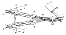
光学MEMS装置のサイズおよび/または有効な傾斜範囲に対する制約のために、全光学スイッチにおけるポート数に対する制限は、組み合わされる各光学MEMS装置のサイズを有する単一の仮想光学MEMS装置を形成するために、実際の他の光学MEMS装置またはその像とを組み合わせる像形成システムを使用する、1つまたは複数の光学MEMS装置の像形成によって、本発明の原理によって解消されることができる。これは、図1に見ることができ、図1は、組み合わされる各光学MEMS装置のサイズを有する仮想光学MEMS装置を形成するために、各2つの光学MEMS装置が、それぞれ像形成システムを使用して像形成される、全光学スイッチング構成の一実施形態を示す。a)第1の入力ファイバ束101、b)第1の入力マイクロ・レンズ・アレイ102、c)第1の入力MEMS装置103、d)レンズ105、e)レンズ109、f)第2の入力ファイバ束111、g)第2の入力マイクロ・レンズ・アレイ112、h)第2の入力MEMS装置113、i)レンズ115、j)レンズ119、k)第1の出力ファイバ束121、l)第1の出力マイクロ・レンズ・アレイ122、m)第1の出力MEMS装置123、n)プリズム141、およびo)フィールド・レンズ143が、図1に示されている。
【0020】
第1の入力ファイバ束101は、スイッチされる光信号を供給する。より詳細には、第1の入力ファイバ束101の各ファイバは、図1のスイッチング・システムに対する入力ポートである。第1の入力ファイバ束101の各ファイバによって供給される光は、第1の入力マイクロ・レンズ・アレイ102の一部であるそれぞれ対応するマイクロ・レンズを通過する。各マイクロ・レンズの機能は、そのそれぞれ結合される入力ファイバから供給された光のビームをコリメートする。本発明の代わりの実施形態において、別個のマイクロ・レンズ・アレイを用いる代わりに、レンズが、コリメータを形成する構成において入力ファイバ束101の各ファイバと統合されることができる。
【0021】
第1の入力マイクロ・レンズ・アレイ102を通過する光の各ビームは、それぞれ第1の入力MEMS装置103のマイクロ・ミラーに当る。第1の入力MEMS装置103の各マイクロ・ミラーは、それぞれ指定された角度で、各マイクロ・ミラーに入射する光のビームを反射するために設定される。特定の指定された角度は、第1の出力MEMS装置123の対応するそれぞれのマイクロ・ミラーの角度との組み合わせで、光が、第1の出力ファイバ束121における事前選択されたファイバに向けられるように選択される。
【0022】
その特定のマイクロ・ミラーの反射後、光の各ビームは、レンズ105およびレンズ109を介してプリズム141を通過する。レンズ105およびレンズ109は、像形成システムを形成する。像形成システムは、プリズム141で作られる各ビームの入射角度が、第1の入力MEMS装置103の各マイクロ・ミラーの角度の関数である。本発明のより簡単な実施形態において、像形成システムは、プリズム141での第1の入力MEMS装置103の各マイクロ・ミラーからの光の反射角度を再現するように構成される。したがって、プリズム141の位置に対する、第1の入力MEMS装置103の各マイクロ・ミラーの直接像形成がある。像形成システムを作り上げる2つのレンズが示されているが、これは、教える目的および明瞭にする目的だけのためであることに留意されたい。当業者は、任意の像形成システム、例えば1つまたは複数のレンズを使用するシステムを用いることができることを容易に理解するであろう。
【0023】
本発明の一実施形態において、4fシステムとしても知られているテレセントリック・システムを、像形成システムとして用いる。従来技術において良く知られているテレセントリック・システムを使用することによって、第1の入力MEMS装置103からの各ビームの光の反射角度は、その光がプリズム141に到達したときに再現される。テレセントリック・システムは反転されることができるので、第1の出力MEMS装置123のそれぞれ対応するマイクロ・ミラーは、それらが用いられない像形成システムを有するとき、同じ場所ではないことができることに留意されたい。しかしながら、マイクロ・ミラーのマッピングの1対1の性質が、像形成システムによって保存されるので、像からの光を、第1の出力ファイバ束121の指定された出力ファイバへ向けるために、第1の出力MEMS装置123のマイクロ・ミラーを適切に傾斜することを、システムの制御ソフトウエアにおいて、反転を容易に考慮することができる。
【0024】
像形成システムは、オリジナルと比べて像のサイズを変更することもできることに留意されたい。これは、第1の出力MEMS装置123のマイクロ・ミラーが、第1の入力MEMS装置103のマイクロ・ミラーと異なるサイズであることを可能にし、ならびに、第1の出力MEMS装置123のマイクロ・ミラーの間隔が、第1の入力MEMS装置103のマイクロ・ミラーの間隔と異なることを可能にする。しかしながら、そうすることが、像において現れたときに、像を第1の出力MEMS装置123のマイクロ・ミラーに適切に向けるために、実際の傾斜の補足的な補償を必要とする、第1の入力MEMS装置103の各マイクロ・ミラーの傾斜角度を同じ縮尺にする。
【0025】
さらに、システムを通る多数の信号経路を作るために、例えば、マルチキャスト、ブロードキャスト、監視、保護、および復元機能を実施するために、例えばレンズ105と109との間に光スプリッタを用いることが可能である。有利には、システム設計における大きな柔軟性が達成される。
【0026】
第2の入力ファイバ束111は、同様にスイッチされる光信号を提供する。より詳細には、第2の入力ファイバ束111の各ファイバは、同様に図1のスイッチング・システムに対する入力ポートである。第2の入力ファイバ束111の各ファイバによって提供される光は、第2の入力マイクロ・レンズ・アレイ112の一部であるそれぞれ対応するマイクロ・レンズを通過する。各マイクロ・レンズの機能は、そのそれぞれ結合される入力ファイバから供給された光のビームをコリメートする。本発明の代わりの実施形態において、別個のマイクロ・レンズ・アレイを用いる代わりに、レンズが、コリメータを形成する構成において第2の入力ファイバ束111の各ファイバと統合されることができる。
【0027】
第2の入力マイクロ・レンズ・アレイ112を通過する光の各ビームは、それぞれ第2の入力MEMS装置113のマイクロ・ミラーに当る。第2の入力MEMS装置113の各マイクロ・ミラーは、それぞれ指定された角度で、各マイクロ・ミラーに入射する光のビームを反射するために設定される。特定の指定された角度は、第1の出力MEMS装置123の対応するそれぞれのマイクロ・ミラーの角度との組み合わせにおいて、光が、第1の出力ファイバ束121における事前選択されたファイバに向けられるように選択される。
【0028】
その特定のマイクロ・ミラーの反射後、光の各ビームは、レンズ115およびレンズ119を介してプリズム141を通過する。レンズ115およびレンズ119は、像形成システムを形成する。像形成システムは、第2の入力MEMS装置113の各マイクロ・ミラーの角度が、プリズム141で再現されるように構成される。したがって、プリズム141の位置に対して、第2の入力MEMS装置113の各マイクロ・ミラーの直接像形成がある。像形成システムを作り上げる2つのレンズが示されているが、これは、教える目的および明瞭にする目的だけのためであることに留意されたい。当業者は、任意の像形成システム、例えば1つまたは複数のレンズを使用するシステムを用いることができることを容易に理解するであろう。
【0029】
本発明の一実施形態において、4fシステムとしても知られているテレセントリック・システムを、像形成システムとして用いる。従来技術において良く知られているテレセントリック・システムを使用することによって、第2の入力MEMS装置115からの各ビームの光の反射角度は、その光がプリズム141に到達したときに再現される。テレセントリック・システムは反転されることができるので、第1の出力MEMS装置123のそれぞれ対応するマイクロ・ミラーは、それらが用いられない像形成システムを有するとき、同じ場所ではないことができることに留意されたい。しかしながら、マイクロ・ミラーのマッピングの1対1の性質が、像形成システムによって保存されるので、反転を、像からの光を、第1の出力ファイバ束121の指定された出力ファイバへ向けるために、第1の出力MEMS装置123のマイクロ・ミラーを適切に傾斜することを、システムの制御ソフトウエアにおいて容易に考慮することができる。テレセントリック・システムを作り上げる2つのレンズが示されているが、これは、教える目的および明瞭にする目的だけのためであることに留意されたい。当業者は、任意のテレセントリック・システム、例えばより多くのレンズを使用するシステムを用いることができることを容易に理解するであろう。
【0030】
像形成システムは、オリジナルと比べて像のサイズを変更することもできることに留意されたい。これは、第1の出力MEMS装置123のマイクロ・ミラーが、第2の入力MEMS装置113のマイクロ・ミラーと異なるサイズであることを可能にし、ならびに、第1の出力MEMS装置123のマイクロ・ミラーの間隔が、第2の入力MEMS装置113のマイクロ・ミラーの間隔と異なることを可能にする。しかしながら、そうすることが、像において現れたときに、像を第1の出力MEMS装置123のマイクロ・ミラーに適切に向けるために、実際の傾斜の補足的な補償を必要とする、第2の入力MEMS装置113の各マイクロ・ミラーの傾斜角度を同じ縮尺にする。
【0031】
さらに、システムを通る多数の信号経路を作るために、例えば、マルチキャスト、ブロードキャスト、監視、保護、および復元機能を実施するために、例えばレンズ115と119との間に光スプリッタを用いることが可能である。有利には、システム設計における大きな柔軟性が達成される。
【0032】
プリズム141の機能は、第1の入力MEMS装置103の像、および第2の入力MEMS装置113の像の経路を曲げることである。図1に示される本発明の実施形態において、プリズム141を通過した後、プリズム141の中心を通るフィールド・レンズ143の中心を通過する線に沿って交わる点で第1の入力MEMS装置103および第2の入力MEMS装置113が互いに隣接するように生じた像が現れるように、曲げが実行される。したがって、本発明の原理によれば、第1の入力MEMS装置103および第2の入力MEMS装置113の組み合わせられたサイズを有する、単一の入力MEMS装置で作られる。この像は、仮想MEMS入力装置として作用する。
【0033】
図1に示される本発明の実施形態において、プリズム141は、少なくとも2つのセクションを有し、1つのセクションは、第1の入力MEMS装置103の像を曲げるためのものであり、他のセクションは、第2の入力MEMS装置113の像を曲げるためのものである。実際に、2つのセクションは、別個のプリズムであることができ、または、単一の統合された装置を用いることができる。好ましくは、第1の入力MEMS装置103の像の全光ビームは、同じ量で曲げられ、同様に、第2の入力MEMS装置113の像の光ビームは、全て同じで曲げられる。しかしながら、第1の入力MEMS装置103の像の全光ビームが曲げられる量は、第2の入力MEMS装置113の像の全光ビームが曲げられる量と必ずしも同じではない。当業者は、プリズム141の機能は、同様に、様々な他のレンズ構成で実行されることができることを理解するであろう。プリズム141の機能を実行する特定の構成は、価格および全体の光学システム・アーチテクチャ、すなわち用いられる全体のレンズ・システムを考慮する設計に基づいて選択される。
【0034】
組み合わせられる光学MEMS装置の像の光は、第1の出力MEMS装置123へのその経路で任意選択のフィールド・レンズ143を通過する。任意選択のフィールド・レンズは、光が入射される角度を、光が向けられる位置における各マイクロ・ミラーへ変換する。これは、第1の入力MEMS装置103および第2の入力MEMS装置113の全てのマイクロ・ミラーが、均一になることを可能にし、同じ傾斜を有する全てのマイクロ・ミラーが、同じ位置にそれらの光を向ける。さらに、フィールド・レンズは、それを通過する各ビームを再集束し、したがって損失を低減する。
【0035】
各フィールド・レンズ143を通る光のビームは、第1の出力MEMS装置123のそれぞれマイクロ・ミラーに当る。第1の出力MEMS装置123の各マイクロ・ミラーは、それぞれの角度で、各マイクロ・ミラーに入射する光のビームを反射するために設定される。マイクロ・ミラーへの入射光は、光を受けるためのものであり、かつその光に関する出力ポートとして作用する第1の出力ファイバ束121の特定のファイバへ反射するように、特定の角度が選択される。
【0036】
第1の出力MEMS装置123の各マイクロ・ミラーを通る光のビームは、マイクロ・レンズ・アレイ122のそれぞれのマイクロ・レンズを通過する。各マイクロ・レンズの機能は、光ビームを、それぞれ結合される出力ファイバに結合するものである。本発明の代わりの実施形態において、別個のマイクロ・レンズ・アレイを用いる代わりに、レンズが、コリメータを形成する構成におけるファイバ束121の出力ファイバの各ファイバと統合されることができる。それから、マイクロ・レンズ・アレイ122の各マイクロ・レンズからの光は、マイクロ・レンズに結合されるそれぞれの出力ファイバ束を通る。
【0037】
図1に示される本発明の実施形態は、例えば、入力ポートの数が出力ポートの数より大きい非対称システムに特に有用である。
【0038】
図2は、全光学スイッチング構成の一実施形態を示し、2つの入力光学MEMS装置が、組み合わされる各入力光学MEMS装置のサイズを有する仮想入力光学MEMS装置を形成するために、像形成システムを用いて像形成され、2つの出力光学MEMS装置が、組み合わされる各出力光学MEMS装置のサイズを有する仮想出力光学MEMS装置を形成するために、像形成システムを用いて像形成される。a)第1の入力ファイバ束101、b)第1の入力マイクロ・レンズ・アレイ102、c)第1の入力MEMS装置103、d)レンズ105、e)レンズ109、f)第2の入力ファイバ束111、g)第2の入力マイクロ・レンズ・アレイ112、h)第2の入力MEMS装置113、i)レンズ115、j)レンズ119、k)第1の出力ファイバ束121、l)第1の出力マイクロ・レンズ・アレイ122、m)第1の出力MEMS装置123、n)プリズム141、o)フィールド・レンズ143、q)レンズ225、r)レンズ229、s)第2の出力ファイバ束231、t)第2の出力マイクロ・レンズ・アレイ232、u)第2の出力MEMS装置233、v)レンズ235、w)レンズ239、およびx)プリズム245が、図2に示されている。
【0039】
入力セクション、すなわちフィールド・レンズ143の左側の図2に示される全ての要素、およびその作用、ならびにフィールド・レンズ143およびその作用は、図1の同様の符号が付けられた構成部品に関する記載と同様である。
【0040】
同様に、フィールド・レンズ143の右側の図2の全ての要素は、反転する方法で作用する。したがって、第1の出力光学MEMS装置123および第2の光学MEMS装置233の組み合わせられたサイズを有するMEMS装置の像は、それぞれa)レンズ225およびレンズ229と、b)レンズ235およびレンズ239と、プリズム245から作られる像形成システムによって形成される。この像は、仮想MEMS出力装置として作用する。組み合わされた出力光学MEMS装置の像の特定のマイクロ・ミラーの像に当るフィールド・レンズ143からの光は、像形成される実際のマイクロ・ミラーに像を投射するそれぞれの像形成システムを通って進む。その光は、このマイクロ・ミラーを反射し、マイクロ・レンズを通過し、出力マイクロ・ミラーが向けられる出力ファイバを通過するように向けられる。
【0041】
より詳細には、組み合わせられた入力光学MEMS装置の像の光が、任意選択のフィールド・レンズ143を通過した後、その光はプリズム141の逆の機能を実行するプリズム245に入射し、それは入射光を2つの方向に向け、その第1は、レンズ225およびレンズ229から作られる像形成システムを通り、その第2は、レンズ235およびレンズ239から作られる像形成システムを通る。第1の出力MEMS装置123の像に対応する点で、プリズム245に入射するこれらのビームは、レンズ225および229から作られる像形成システムまで、プリズム245によって向けられる。同様に、第2の出力MEMS装置233の像に対応する点で、プリズム245に入射するこれらのビームは、レンズ235および239から作られる像形成システムまで、プリズム245によって向けられる。
【0042】
像形成システムから作られる2つのレンズが示されるが、これは、教える目的および明瞭にする目的だけのためであることに留意されたい。当業者は、任意の像形成システム、すなわち1つまたは複数のレンズを使用するシステムを用いることができることを容易に理解するであろう。
【0043】
本発明の一実施形態において、レンズ225および229と、レンズ235および239から作られる像形成システムは、4fシステムとしても知られる各テレセントリック・システムである。従来技術において良く知られているテレセントリック・システムを使用することによって、各ビームの光が、プリズム245から各像形成システムに入るとき、各ビームの光の反射角度は、その光が出力MEMS装置123および233のそれぞれ1つに到達したときに再現される。テレセントリック・システムは反転されることができるので、出力MEMS装置123および233のそれぞれ1つの対応する各マイクロ・ミラーは、それらが用いられない像形成システムを有するとき、同じ場所ではないことができることに留意されたい。しかしながら、マイクロ・ミラーのマッピングの1対1の性質が、像形成システムによって保存されるので、像からの光を指定された出力ファイバへ向けるために、マイクロ・ミラーを適切に傾斜することを、システムの制御ソフトウエアにおいて、反転を容易に考慮することができる。
【0044】
像形成システムは、同じ原理の理由のため、オリジナルと比べて像のサイズを変更することもでき、図2に示される光学スイッチング構成の入力セクションに関連して上述されたように、同じ設計の考慮を必要とする。同様に、同じ原理の理由のため、像形成システムにおいて光スプリッタを用いることが可能であり、図2に示される光学スイッチング構成の入力セクションに関連して上述されたように、同じ設計の考慮を必要とする。
【0045】
レンズ225および229の像形成システムを通る各光のビームは、第1の出力MEMS装置123のそれぞれのマイクロ・ミラーに当る。図1に関連して上述したように、第1の出力MEMS装置123の各マイクロ・ミラーは、それぞれの角度で入射光のビームを反射するために設定される。特定の角度は、マイクロ・ミラーの入射光は、光を受けるためのものであり、その光の出力ポートとして作用する第1の出力ファイバ束121の特定のファイバに反射するように選択される。
【0046】
第1の出力MEMS装置123の各マイクロ・ミラーを通る光のビームは、マイクロ・レンズ・アレイ122のそれぞれのマイクロ・レンズを通過する。各マイクロ・レンズの機能は、光ビームを、それぞれ結合される出力ファイバに結合することである。本発明の代わりの実施形態において、別個のマイクロ・レンズ・アレイを用いる代わりに、レンズは、コリメータを形成する構成におけるファイバ束121の各ファイバに統合されることができる。それから、マイクロ・レンズ・アレイ122の各マイクロ・レンズからの光は、マイクロ・レンズに結合されるそれぞれ出力ファイバ束を通過する。
【0047】
同様に、レンズ235および239の像形成システムを通る光の各ビームは、第2の出力MEMS装置233のそれぞれのマイクロ・ミラーに当る。第2の出力MEMS装置233の各マイクロ・ミラーは、入射光のビームをそれぞれの角度で反射するように設定される。特定の角度は、マイクロ・ミラーに入射する光を、光を受けるものであり、かつ光の出力ポートとして作用する第2の出力ファイバ束231の特定のファイバへ反射するように選択される。
【0048】
第2の出力MEMS装置233の各マイクロ・ミラーを通る光のビームは、マイクロ・レンズ・アレイ232のそれぞれのマイクロ・レンズを通過する。各マイクロ・レンズの機能は、それぞれ結合される入力ファイバに供給される光のビームをコリメートすることである。本発明の代わりの実施形態において、別個のマイクロ・レンズ・アレイを用いる代わりに、レンズは、コリメータを形成する構成において、ファイバ束231の各出力ファイバと統合されることができる。それから、マイクロ・レンズ・アレイ232の各マイクロ・レンズからの光は、マイクロ・レンズと結合されるそれぞれの出力ファイバ束内を通過する。
【0049】
実際に、仮想入力MEMS装置および仮想出力MEMS装置が作られ、仮想出力MEMS装置および仮想入力MEMS装置が交差接続を形成するように構成される。
【0050】
図2のシステムが、動作において全体に対称であることに留意されたい。したがって、入力ポートは、出力ポートとして使用されることができ、反対もまた同様である。しかしながら、さらなるものがない図2の構成を仮定すれば、右の任意の1つのファイバに結合される左の1つのファイバだけであることができる。
【0051】
図3は、全光学スイッチング構成のコンパクトな実施形態を示し、2つの入力光学MEMS装置が、組み合わされる各入力光学MEMS装置のサイズを有する仮想入力光学MEMS装置を形成するために、像形成システムを用いて像形成され、2つの出力光学MEMS装置が、組み合わされる各出力光学MEMS装置のサイズを有する仮想出力光学MEMS装置を形成するために、像形成システムを用いて像形成される。図2に示される同じ要素、および追加の要素ミラー307、317、327および337が、図3に示される。図3の全ての要素の作用は、図1および図2の同様の符号が付けられた構成部品に関する記載と同じである。しかしながら、それらの経路に沿った光ビームの方向が、ミラー307、317、327、および337によって反転されるので、それぞれ像形成システムの一部である、マイクロ・レンズ・アレイ、ならびにレンズ109、115、225、および235に結合される、ファイバ束の位置および/または方向は変更される。これは、当業者には理解されるように、図3に示されるよりコンパクトな光学経路を実現することを可能にする。ミラー307、317、327、および337は、それぞれの像形成システム内に配置されるが、像形成の作用は、ミラーが存在しないのと同様に残ることができる。代わりに、ミラー307、317、327、および337の1つまたは複数は、例えばミラーを曲げることによって、その結合される像形成システム内の光の方向を変更するより、それらのそれぞれの像形成システムに作用的な効果を有するようにすることができる。
【0052】
図4は、システムが折りたたまれる本発明の他の例示的実施形態を示す。a)第1のファイバ束401、b)第1のマイクロ・レンズ・アレイ402、c)第1のMEMS装置103、d)レンズ105、e)レンズ109、f)第2のファイバ束411、g)第2のマイクロ・レンズ・アレイ412、h)第2のMEMS装置113、i)レンズ115、j)レンズ119、k)プリズム141、l)ミラー307および317、およびm)フォールディング・ミラー413が、図4に示されている。
【0053】
前述の実施形態とは異なり、ファイバ束401は、入力ファイバと出力ファイバの両方を含み、ファイバ束401は、入力ポートおよび出力ポートとして作用する。入力ファイバからの光は、第1のマイクロ・レンズ・アレイ402のそれぞれ結合されるマイクロ・レンズを通過する。光は、第1のMEMS装置103の対応する結合されたマイクロ・ミラーを反射し、図4においてレンズ105および109で作られる像形成システムを通過する。上述に言及したように、像形成システムを作る2つのレンズが示されているが、これは、教える目的および明瞭にする目的だけのためである。当業者は、任意の像形成システム、例えば1つまたは複数のレンズを使用するシステムを用いることができることを容易に理解するであろう。本発明の一実施形態において、テレセントリック・システムを、像形成システムとして用いられる。図4に示される本発明の一実施形態において、それを通過する光は、ミラー307によって再び方向付けられるので、像形成システムは、コンパクトな像形成システムである。
【0054】
同様に、ファイバ束411は、入力ファイバおよび出力ファイバの両方を含み、ファイバ束411は、入力ポートおよび出力ポートとして作用する。入力ファイバからの光は、第1のマイクロ・レンズ・アレイ412のそれぞれ結合されるマイクロ・レンズを通過する。光は、第1のMEMS装置113の対応する結合されたマイクロ・ミラーを反射し、図4においてレンズ115および119で作られる像形成システムを通過する。上述に言及したように、像形成システムを作る2つのレンズが示されているが、これは、教える目的および明瞭にする目的だけのためである。当業者は、任意の像形成システム、例えば1つまたは複数のレンズを使用するシステムを用いることができることを容易に理解するであろう。本発明の一実施形態において、テレセントリック・システムを、像形成システムとして用いられる。図4に示される本発明の一実施形態において、それを通過する光は、ミラー317によって再び方向付けられるので、像形成システムは、コンパクトな像形成システムである。
【0055】
各像形成システムから出る光のビームは、プリズム141を通過する。前に記載した本発明の実施形態のように、像形成システムから来る光に関して、プリズム141の機能は、第1のMEMS装置103の像および第2のMEMS装置113の像の経路を曲げることである。図4に示される本発明の実施形態において、曲げが実行され、プリズム141を通過した後、結果としての像は、まるで、第1のMEMS装置103および第2のMEMS装置113が、ミラー413の中心からプリズム141の中心を通る線に沿って交わる点で、第1のMEMS装置103および第2のMEMS装置113が、互いに隣接するように現れる。したがって、本発明の原理によれば、像は、第1のMEMS装置103および第2のMEMS装置113の組合されたサイズを有する、単一の入力MEMS装置を作る。
【0056】
第1のMEMS装置103および第2のMEMS装置113の像は、ミラー413によって反射される。ミラー413は、平面ミラーとして機能する平坦な従来のミラーであるか、または本明細書に記載される本発明の他の実施形態におけるフィールド・レンズによって実行される機能を組み込むために湾曲されたものであることができる。
【0057】
光のビームは、リターン・ビームとして、ミラー413によってプリズム141に向かって反射されて戻る。プリズム141は、上述されたプリズム245と同じように、リターン・ビームの方向を変更する。より詳細には、像形成システムの1つへのその経路のミラー413から来る光に関して、プリズム141は、ミラー413に向かって進める像形成システムから来る光に関して実行した機能の反対を実行する。このために、プリズム141は、2つの方向にプリズム141に入射する光を向け、第1の方向は、レンズ105およびレンズ109で作られる像形成システムを通り、第2の方向は、レンズ115およびレンズ119で作られる像形成システムを通る。第1のMEMS装置103の像に対応する点で、プリズム141に入射するこれらのビームは、レンズ105および109から作られる像形成システムへ、プリズム141によって向けられる。同様に、第2のMEMS装置113の像に対応する点で、プリズム141に入射するこれらのビームは、レンズ115および119から作られる像形成システムへ、プリズム141によって向けられる。
【0058】
一般に、これは必要要件ではないが、リターン・ビームは、ミラー413に向かってリターン・ミラーを初期的に反射するマイクロ・ミラーとは異なるマイクロ・ミラーを入射し、光の任意の入力ビームに関して、リターン・ビームは、ミラー413に向かって反射する同じマイクロ・ミラーに入射する必要がある可能性がある。そうすることは、ファイバ束における任意のファイバを、それ自体を含むファイバ束における任意の他のファイバへ接続されることを可能にする。
【0059】
その後、各リターン・ビームは、それが向けられるそれぞれ像形成システムを通過し、その後、第1のMEMS装置103および第2のMEMS装置113の対応する1つのマイクロ・ミラーによって、ビームに関する出力ポートとして作用するファイバ束401および411に結合される1つのそれぞれファイバに向かって反射される。マイクロ・ミラーから反射された後であるが、ファイバに入る前に、ビームは、ビームに関する出力ポートとして作用するファイバに結合される、マイクロ・レンズ・アレイ402および422の1つのマイクロ・レンズを通過する。
【0060】
図5は、全光学スイッチング・システムの他の実施形態を示し、図2に示される光学経路と同等の光学経路を有する。しかしながら、プリズム141および245の代わりに、ミラーが図5において用いられ、結果として異なる空間経路に続く光学経路となる。これにより、よりコンパクトなシステム構成の結果となる。図5において、プリズム141および245が取り除かれ、代わりに追加のミラー要素541、551、561、および571が追加された以外は、図2に示されるのと同じ要素が示される。図5の全ての要素の機能は、図1および図2の同様の符号が付けられた構成部品に関する記載と同じである。
【0061】
ミラー541および561の機能は、それらが、第1の入力MEMS装置103の像、および第2の入力MEMS装置113の像の経路を曲げる、プリズム141の機能と同様である。図5に示される本発明の実施形態において、曲げが実行され、ミラー541および561を通過した後、まるで第1の入力MEMS装置103および第2の入力MEMS装置113が、フィールド・レンズ143の中心から、ミラー541および561が交わる点を通る線に沿ってそれらが交わる点で、互いに隣接するように、結果としての像が現れる。しかしながら、プリズムの代わりにミラーを使用することは、光ビームの方向を変更し、それによってよりコンパクトな構造を提供することに留意されたい。したがって、本発明の原理によれば、像は、第1の入力MEMS装置103および第2の入力MEMS装置113の組み合わせたサイズを有する、単一の入力MEMS装置で作られる。この像は、仮想MEMS入力装置として作用する。
【0062】
図5に示される本発明の実施形態において、少なくとも2つの個別ミラーが存在し、一方は、第1の入力MEMS装置103の像を曲げるためのものであり、他方は、第2の入力MEMS装置113の像を曲げるためのものである。実際には、2つのセクションは、単一の統合されたミラーを形成するために結合されることができる。好ましくは、第1の入力MEMS装置103の像の光の全てのビームは、同じ量だけ曲げられ、同様に、第2の入力MEMS装置113の像の光のビームは、すべて同じ量だけ曲げられる。しかしながら、第1の入力MEMS装置103の像の光の全てのビームが曲げられる量は、第2の入力MEMS装置113の像の光の全てのビームが曲げられる量とかならずしも同じではない。当業者は、ミラー541および561の機能は、追加のミラーまたはレンズ機能によって補足されることができる、湾曲したミラーなどの様々なミラー構成で実行されることができることを諒承するであろう。ミラー541および561の機能を実行するための特定の構成は、価格、または全体の光学システム・アーチテクチャなどの設計考慮事項に基づき選択される。
【0063】
ミラー551および571の機能は、それらが、第1の出力MEMS装置123の像、および第2の出力MEMS装置233の像の経路を曲げる、プリズム245の機能と同様である。図5に示される本発明の実施形態において、曲げが実行され、ミラー551および571を通過した後、まるで第1の出力MEMS装置123および第2の出力MEMS装置233が、フィールド・レンズ143の中心から、ミラー551および571が交わる点を通る線に沿ってそれらが交わる点で、互いに隣接するように、結果としての像が現れる。しかしながら、プリズムの代わりにミラーを使用することは、光ビームの方向を変更し、それによってよりコンパクトな構造を提供することに留意されたい。したがって、本発明の原理によれば、像は、第1の出力MEMS装置123および第2の出力MEMS装置233の組み合わせたサイズを有する、単一の出力MEMS装置で作られる。この像は、仮想MEMS出力装置として作用する。
【0064】
図5に示される本発明の実施形態において、少なくとも2つの個別ミラーが存在し、一方は、第1の出力MEMS装置123の像を曲げるためのものであり、他方は、第2の出力MEMS装置233の像を曲げるためのものである。実際には、2つのセクションは、単一の統合されたミラーを形成するために結合されることができる。好ましくは、第1の出力MEMS装置123の像の光の全てのビームは、同じ量だけ曲げられ、同様に、第2の出力MEMS装置233の像の光のビームは、すべて同じ量だけ曲げられる。しかしながら、第1の出力MEMS装置123の像の光の全てのビームが曲げられる量は、第2の出力MEMS装置233の像の光の全てのビームが曲げられる量とかならずしも同じではない。当業者は、ミラー551および571の機能は、追加のミラーまたはレンズ機能によって補足されることができる、湾曲したミラーなどの様々なミラー構成で実行されることができることを諒承するであろう。ミラー551および571の機能を実行するための特定の構成は、価格、または全体の光学システム・アーチテクチャなどの設計考慮事項に基づき選択される。
【0065】
図6は、全光学スイッチング・システムの他の実施形態を示し、実際のMEMS装置のその入力セクションにおける使用のために、MEMS装置の像と組み合わせる。
【0066】
a)第1の入力ファイバ束101、b)第1の入力マイクロ・レンズ・アレイ102、c)第1の入力MEMS装置103、d)レンズ105、e)レンズ109、f)第2の入力ファイバ束111、g)第2の入力マイクロ・レンズ・アレイ112、h)ミラー541、i)第2の入力MEMS装置113、j)プリズム245、k)第1の出力ファイバ束121、l)第1の出力マイクロ・レンズ・アレイ122、m)第1の出力MEMS装置123、n)プリズム245、o)フィールド・レンズ143、q)レンズ225、r)レンズ229、s)第2の出力ファイバ束231、t)第2の出力マイクロ・レンズ・アレイ232、u)第2の出力MEMS装置233、v)レンズ235、およびw)レンズ239が、図6に示されている。
【0067】
第1の入力ファイバ束101は、切り換えられる光学信号を供給する。より詳細には、第1の入力ファイバ束101の各ファイバは、図1のスイッチング・システムの入力ポートである。第1の入力ファイバ束101の各ファイバによって供給される光は、第1の入力マイクロ・レンズ・アレイ102の一部である、それぞれ対応するマイクロ・レンズを通過する。各マイクロ・レンズの機能は、そのそれぞれ結合される入力ファイバから供給される光のビームをコリメートすることである。本発明の代わりの実施形態において、別個のマイクロ・レンズ・アレイを用いる代わりに、レンズが、コリメータを形成する構成における入力ファイバ束101の各ファイバと統合されることもできる。
【0068】
第1の入力マイクロ・レンズ・アレイ102を通過する光の各ビームは、それぞれ第1の入力MEMS装置103のマイクロ・ミラーに当る。第1の入力MEMS装置103の各マイクロ・ミラーは、それぞれ指定された角度で、各マイクロ・ミラーに入射する光のビームを反射するために設定される。特定の指定された角度は、前述され、第1の出力MEMS装置123および第2の出力MEMS装置233の1つの対応するそれぞれのマイクロ・ミラーの角度との組み合わせで、光が、第1の出力ファイバ束121、または第2の出力ファイバ束231のいずれかにおける事前選択されたファイバに向けられるように指定される。
【0069】
その特定のマイクロ・ミラーの反射後、光の各ビームは、レンズ105、次にレンズ109を通過し、ミラー541へ行く。レンズ105およびレンズ109は、像形成システムを形成する。像形成システムは、第1の入力MEMS装置103の各マイクロ・ミラーの角度が、ミラー541で再現されるように構成される。したがって、ミラー541の位置へ、第1の入力MEMS装置103の各マイクロ・ミラーの直接の像形成が存在する。像形成システムを作り上げる2つのレンズが示されているが、これは、教える目的および明瞭にする目的だけのためであることに留意されたい。当業者は、任意の像形成システム、例えば1つまたは複数のレンズを使用するシステムを用いることができることを容易に理解するであろう。
【0070】
本発明の一実施形態において、4fシステムとしても知られているテレセントリック・システムを、像形成システムとして用いる。従来技術において良く知られているテレセントリック・システムを使用することによって、第1の入力MEMS装置103からの各ビームの光の反射角度は、その光がミラー541に到達したときに再現される。テレセントリック・システムは反転されることができるので、第1の出力MEMS装置123のそれぞれ対応するマイクロ・ミラーは、それらが用いられない像形成システムを有するとき、同じ場所ではないことができることに留意されたい。しかしながら、マイクロ・ミラーのマッピングの1対1の性質が、像形成システムによって保存されるので、像からの光を、第1の出力ファイバ束121の指定された出力ファイバへ向けるために、第1の出力MEMS装置123のマイクロ・ミラーを適切に傾斜することを、システムの制御ソフトウエアにおいて、反転を容易に考慮することができる。
【0071】
像形成システムは、オリジナルと比べて像のサイズを変更することもできることに留意されたい。これは、第1の出力MEMS装置123のマイクロ・ミラー、および第2の出力MEMS装置233のマイクロ・ミラーが、第1の入力MEMS装置103のマイクロ・ミラーと異なるサイズであることを可能にし、ならびに、第1の出力MEMS装置123および第2の出力MEMS装置233のマイクロ・ミラーの間隔が、第1の入力MEMS装置103のマイクロ・ミラーの間隔と異なることを可能にする。しかしながら、そうすることが、像において現れたときに、像を第1の出力MEMS装置123、および第2の出力MEMS装置233のマイクロ・ミラーに適切に向けるために、実際の傾斜の補足的な補償を必要とする、第1の入力MEMS装置103の各マイクロ・ミラーの傾斜角度を同じ縮尺にする。
【0072】
さらに、システムを通る多数の信号経路を作るために、例えば、マルチキャスト、ブロードキャスト、監視、保護、および復元機能を実施するために、例えばレンズ105と109との間に光スプリッタを用いることが可能である。有利には、システム設計における大きな柔軟性が達成される。
【0073】
第2の入力ファイバ束111は、同様にスイッチされる光信号を提供する。より詳細には、第2の入力ファイバ束111の各ファイバは、同様に図1のスイッチング・システムに対する入力ポートである。第2の入力ファイバ束111の各ファイバによって提供される光は、第2の入力マイクロ・レンズ・アレイ112の一部であるそれぞれ対応するマイクロ・レンズを通過する。各マイクロ・レンズの機能は、そのそれぞれ結合される入力ファイバから供給された光のビームをコリメートする。本発明の代わりの実施形態において、別個のマイクロ・レンズ・アレイを用いる代わりに、レンズが、コリメータを形成する構成において第2の入力ファイバ束111の各ファイバと統合されることができる。
【0074】
第2の入力マイクロ・レンズ・アレイ112を通過する光のビームは、それぞれ第2の入力MEMS装置113のマイクロ・ミラーに当る。第2の入力MEMS装置113の各マイクロ・ミラーは、それぞれ指定された角度で、各マイクロ・ミラーに入射する光のビームを反射するために設定される。特定の角度は、第1の出力MEMS装置123、または第2の出力MEMS装置233の対応するそれぞれのマイクロ・ミラーの角度との組み合わせで、光が、第1の出力ファイバ束121、または第2の出力ファイバ束231における事前選択されたファイバに向けられるように指定される。
【0075】
その特定のマイクロ・ミラーの反射後、光の各ビームはフィールド・レンズ143を通る。
【0076】
ミラー541の機能は、第1の入力MEMS装置103の像の経路を曲げることであり、まるで第1の入力MEMS装置103が、フィールド・レンズ143の中心から、プリズム245の中心を通過する線に沿って、像と実際のMEMS装置が交わる点で、第2の入力MEMS装置113に隣接するように、結果としての像が現れる。したがって、本発明の原理によれば、第1の入力MEMS装置103および第2の入力MEMS装置113の組み合わせたサイズを有する、単一の入力MEMS装置が存在するように現れる。この組み合わせは、仮想MEMS入力装置である全体の入力MEMS装置として作用する。
【0077】
フィールド・レンズ143を通過した後、光は、スイッチング・システムの出力セクション、すなわち図6におけるフィールド・レンズ143の右側の全ての要素に入る。フィールド・レンズ143および図6の出力セクションの動作は、図2の出力セクションの同様の符号が付けられた構成部品に関する記載と同様である。
【0078】
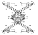
教える目的および明瞭にする目的のために、示された実施形態は、多くとも2つのMEMS装置の入力セクションまたは出力セクションに関して、それらの像または実際部分と像部分とを組み合わせただけであることに留意されたい。しかしながら、例えば実施形態が示される紙面の外に、例えば前述の実施形態を三次元に構成することによって、2つ以上のMEMS装置が積み重ねられた、本発明の実施形態を有することは可能である。そのような構成は、MEMS装置またはそれらの像が、入力、出力、またはその両方に関してより大きな仮想MEMS装置さえも作り出すために、「タイル状に(tiled)」されることを可能にする。図7は、いくつかの可能な様々なタイル構成である、MEMS装置またはそれらの像のためのタイル構成701、702、および703を示す。当業者には、他のそのような構成を開発することが容易に可能であろう。
【0079】
図8は、4つの出力MEMS装置の像が、1つの大きな出力MEMS装置を形成するために結合される、1つのそのような構成の端部図である。図8において見えないが、それらは、図8に示される要素の真後ろであるため、4つの入力MEMS装置は、同様に1つの大きな入力MEMS装置を形成するために結合される。代わりに、図8は、出力セクションの端部図であるが、反対側から見た図であると考えることができる。図1に示される要素の数は、図2の同様の符号が付けられた要素に機能的に対応するが、図2に元々示された要素に1のサフィックスが追加され、より大きなアレイを形成するために図8に導入された要素に2のサフィックスが追加されている。
【0080】
当業者は、システムの様々な構成部品およびミラーの所望のサイズおよび構成を達成するために、それらをどのように向けるかについて容易に理解するであろう。
【0081】
入力として光を供給する光ファイバの代わりに、光が、例えば、レーザまたは発光ダイオード、プレーナ導波路などの光源によって供給されることができることに留意されたい。同様に、出力として光ビームを受ける光ファイバを有する代わりに、光ビームが、光検出器、プレーナ導波路などの他の受信器によって受け取られることができる。
【図面の簡単な説明】
【図1】全光学スイッチング構成の一実施形態を示し、各2つの光学MEMS装置が、組み合わされる各MEMS装置のサイズを有する仮想光学MEMS装置を形成するために、それぞれ像形成システムを用いて像形成される図である。
【図2】全光学スイッチング構成を示し、2つの入力光学MEMS装置が、組み合わされる各入力光学MEMS装置のサイズを有する仮想入力光学MEMS装置を形成するために、像形成システムを用いて像形成され、2つの出力光学MEMS装置が、組み合わされる各出力光学MEMS装置のサイズを有する仮想出力光学MEMS装置を形成するために、像形成システムを用いて像形成される図である。
【図3】全光学スイッチング構成のコンパクトな実施形態を示し、2つの入力光学MEMS装置が、組み合わされる各入力光学MEMS装置のサイズを有する仮想入力光学MEMS装置を形成するために、像形成システムを用いて像形成され、2つの出力光学MEMS装置が、組み合わされる各出力光学MEMS装置のサイズを有する仮想出力光学MEMS装置を形成するために、像形成システムを用いて像形成される図である。
【図4】システムが折りたたまれる本発明の例示的実施形態を示す図である。
【図5】図2に示される光学経路と同等の光学経路を有するが、図2のプリズムの代わりにミラーが用いられた全光学スイッチング・システムを示す図である。
【図6】その入力セクションにおいて実際のMEMS装置を使用するために、MEMS装置の像と組み合わす全光学スイッチング・システムの他の実施形態を示す図である。
【図7】いくつかの可能なタイル状構成を示す図である。
【図8】4つの出力MEMS装置の像が、ある大きな出力MEMS装置からまたは出力MEMS装置へ結合されるあるタイル状構成の端と端とが向き合った図である。[0001]
BACKGROUND OF THE INVENTION
The present invention relates to optical-electromechanical system (MEMS) technology, and more particularly to all-optical switching using MEMS devices.
[0002]
[Prior art]
One solution for all-optical switching uses two MEMS devices. Each MEMS device includes a tiltable micro lens, for example an array of small mirrors, that reflects light, referred to herein as any radiation at the wavelength of interest, whether in the visible spectrum or not. be able to. An optical path has a second micro on the second optical MEMS device coupled to the output fiber using a first micro mirror that couples light to the input fiber on the first optical MEMS device. Established by directing to a mirror, for light supplied from an input source, for example an optical fiber, to an output, for example an output fiber. The second micro mirror then directs the light to the output fiber. Each fiber connected to the system is considered a port of the system, with the input fiber being the input port and the output fiber being the output port.
[0003]
[Problems to be solved by the invention]
The problem with all-optical switching technology using MEMS devices is that in order to increase the number of ports in the system, ie the number of fibers, it is necessary to increase the number of micro mirrors used to perform the switching function. It is. In the prior art, as described above, the first optical MEMS device includes all the first micro mirrors integrated thereon, and the second optical MEMS device includes all the first micro mirrors integrated thereon. Includes a second micro mirror. The size of the optical MEMS device is a direct function of the number of micro mirrors on the optical MEMS device, and the number of micro mirrors required is directly proportional to the maximum number of ports available in all optical switches, so in all optical switches Increasing the maximum number of ports that can be used requires the use of larger optical MEMS devices.
[0004]
Unfortunately, limitations on manufacturing capacity and large package size currently limit optical MEMS devices to 1296 micro mirrors. Furthermore, even if the size of the micro mirror can be effectively reduced, there is still a problem that a control signal needs to be transmitted to each micro mirror. The routing of these control signals consumes a large space of the optical MEMS device, resulting in a very large optical MEMS device. In addition, there are control signals for each micro mirror that must be transmitted from the substrate to the optical MEMS device. In order to make these connections, more space is required in the optical MEMS device.
[0005]
As a result of all these space requirements, optical MEMS chips are quite large, where manufacturing capacity limitations limit the number of micro mirrors that can be placed on a single optical MEMS device. Secondly, the limitation on the number of micro mirrors limits the number of ports of all optical switches.
[0006]
Moreover, currently available micro mirrors have a limited effective range that can be tilted. Each micro mirror on the first optical MEMS device must be able to direct incident light on each micro mirror to each micro mirror on the second optical MEMS device, so there is a limitation in effective range. Furthermore, it limits the number of ports that can be implemented in all optical switches using such optical MEMS devices. The ability to direct light in this way is a function of the effective tilt range of the micro mirror. In other words, a larger effective tilt angle allows each micro mirror to direct its light to a larger area. For an optical MEMS device arranged as an optical switch, the largest tilt angle required is for the connection between the micro mirrors at the opposite corner of the optical MEMS device. For example, the greatest tilt is required for the micro mirror at the right top of the first MEMS device, where the light must be directed to the micro mirror at the left bottom of the second MEMS device. Thus, the size of the micro mirror array that can be used in an optical switch is limited by the effective tilt range of the optical MEMS device.
[0007]
Increasing the separation distance between two optical MEMS devices reduces the required tilt angle and allows the use of larger micro mirror arrays without changing the effective tilt range of the micro mirror To do. However, doing so increases the beam diffraction and necessitates the use of micro-mirrors with a larger diameter, which results in some light loss. Since using larger micro mirrors requires more space, doing so increases the distance between the micro mirrors on the optical MEMS device, and the optical MEMS device's for the same number of micro mirrors. Increase the size further. As a result of increasing the size of the optical MEMS device, a larger tilt angle needs to combine the opposite corners of the opposing optical MEMS device. Thus, in essence, further separation of opposing optical MEMS devices does not help to increase the number of ports due to limited available tilt angles.
[0008]
Furthermore, because the package of MEMS devices is significantly larger than the area containing the micro mirrors, the micro mirror arrays of multiple optical MEMS devices are directly adjacent to each other to form a single, composite, larger MEMS device. The current design to be placed is not possible. Future designs may not be easy to do as it requires a larger end area on the optical MEMS device to make the many connections needed.
[0009]
[Means for Solving the Problems]
Due to constraints on the size of the optical MEMS device and / or the effective tilt angle, the limitation on the number of ports in the all-optical switch is to form a single virtual optical MEMS device with the size of each optical MEMS device coupled. It has been found that the principles of the present invention can be solved by imaging one or more optical MEMS devices using an imaging system in combination with other actual optical MEMS devices or images thereof. The physical size of the configuration can be duplicated for both input and output, for example using a suitable conventional mirror and / or using a folded configuration, ie by using at least one conventional mirror. This can be reduced by shrinking the optical path using a configuration where there is only one MEMS device stage that performs duty. In one embodiment of the present invention, the imaging system reproduces the reflection angle of light from the micro mirror. This can be achieved using a telecentric system, also known as a 4f system.
[0010]
In an alternative embodiment of the present invention, the imaging system can be at different angles from each other and optically furthest away from the micro-mirror to combine multiple optical MEMS device images and / or actual devices. It may also be necessary for the lenses of the imaging system to overlap each other. In order to compensate for such different angles and overlaps, in one embodiment of the present invention, a prism can be inserted for each image of the optical MEMS device in the plane in which the image is formed. The prism is between the lens of the imaging system for the optical MEMS device furthest away from the optical MEMS device and at least the lens of the imaging system of another optical MEMS device furthest from the other optical MEMS device. And all angles of light with respect to the opposite optical MEMS device. In one embodiment of the invention, a lens can be used instead of a prism to perform the same function. Furthermore, in other embodiments of the invention, folding mirrors can be used as well.
[0011]
The entire system is configured taking into account any inversion of the MEMS device depending on the imaging system used.
[0012]
DETAILED DESCRIPTION OF THE INVENTION
The following merely illustrates the principles of the invention. Accordingly, those of ordinary skill in the art may devise various configurations that are not explicitly described or shown herein, but that embody the principles of the invention and fall within the spirit and scope of the invention. You will understand that. Further, all examples and conventional languages described herein are intended to help the reader in understanding the principles and concepts of the present invention as constructed by the inventor, in principle, to advance the technology. Are intended to be for teaching purposes only and are not limited to such specific described examples and conditions. Moreover, all statements herein reciting principles, aspects, and embodiments of the invention, as well as specific examples thereof, are intended to include structural and functional equivalents thereof. . Further, such equivalents include both currently known equivalents as well as equivalents developed in the future, i.e., all elements developed that perform the same function regardless of configuration.
[0013]
Thus, for example, it will be appreciated by those skilled in the art that all block diagrams herein represent conceptual diagrams of exemplary circuits that employ the principles of the present invention. Similarly, all flowcharts, flowcharts, state transition diagrams, pseudocodes, etc. are represented in substantially computer-readable media and, therefore, such computers or processors may be clearly shown. Fig. 7 illustrates various processes performed by a computer or processor without.
[0014]
The functions of the various elements shown in the figure, including any functional blocks labeled as “processors”, are achieved through the use of dedicated hardware as well as hardware capable of executing software that cooperates with the appropriate software. Can be offered. When provided by a processor, the functionality can be provided by a single dedicated processor, a single shared processor, or multiple individual processors, some of which are shared. Furthermore, the explicit use of the terms “processor” or “controller” should not be construed as referring solely to hardware capable of executing software, but as a digital signal processor (DSP). , Network processors, Application Specific Integrated Circuits (ASICs), Field Programmable Gate Arrays (FPGAs), read-only memories for storing software (Read-Only Memories) ROM), random access memory (RAM), non-volatile storage device It may include implicitly without limitation. Other hardware, conventional and / or custom, can be included as well. Similarly, any switches shown in the figures are conceptual only. These functions can be performed through the operation of program logic, through dedicated logic, through the interaction of program control and dedicated logic, or even manually, and certain technologies are Can be selected by the practitioner who is more specifically understood from the context.
[0015]
In the claims of this specification, any element expressed as a means for performing a specific function may be, for example, a) a combination of circuit elements that perform the function, or b) any form of software. As such, including any means to perform that function, including firmware, software including microcode, etc., in combination with appropriate circuitry that implements that software to perform the function. Is intended. The invention defined by such claims is due to the fact that the functionality provided by the various means described is combined and brought together in the manner required by the claims. Applicant thus regards any means that can provide those functionalities as equivalent as those shown herein.
[0016]
A software module, or a simple module, which is meant to be software, is represented herein as a flowchart element or any combination of other elements that indicate the execution of process steps and / or organizational descriptions. Can be done. Such modules can be implemented with hardware that is clearly shown or implied.
Unless otherwise explicitly specified herein, the drawings are not drawn to the same dimensions.
[0017]
In addition, unless expressly specified herein, any lens shown and / or described herein is an actual optical system having the individual specified characteristics of that lens. Such an optical system can be implemented by a single lens element, but is not necessarily limited thereto. Similarly, if a mirror is shown / described, what is actually shown and / or described can be implemented by a single mirror element, but is not necessarily limited to a single mirror element. An optical system with certain characteristics of such mirrors that are not. This is why, as is well known in the prior art, various optical systems can provide the same functionality of a single lens element or mirror, but in an excellent way, for example with less distortion. Furthermore, as is well known in the prior art, the functionality of a curved mirror can be achieved through a lens and mirror combination and vice versa. In addition, the configuration of an optical component that performs a specific function, such as an imaging system, a diffraction grating, a coated element, and a prism, depends on the configuration of any other optical component that performs the same specific function. Can be replaced. Thus, unless expressly specified herein, all optical elements or systems that can provide a particular function in the overall embodiments disclosed herein are equivalent to each other for purposes of this disclosure.
[0018]
The term microelectromechanical system (MEMS) device as used herein is intended to mean the entire MEMS device or any part thereof. Thus, even if some of the MEMS devices cannot operate or are partially blocked, such MEMS devices are still considered MEMS devices for the purposes of this disclosure.
[0019]
Due to constraints on the size of the optical MEMS device and / or the effective tilt range, restrictions on the number of ports in all optical switches are required to form a single virtual optical MEMS device having the size of each optical MEMS device combined. The principles of the present invention can be overcome by imaging one or more optical MEMS devices using an imaging system that combines with other actual optical MEMS devices or images thereof. This can be seen in FIG. 1, which shows that each two optical MEMS devices each use an imaging system to form a virtual optical MEMS device having the size of each optical MEMS device combined. 1 illustrates one embodiment of an all-optical switching configuration that is imaged in this manner. a) first
[0020]
The first
[0021]
Each beam of light that passes through the first input
[0022]
After reflection of that particular micro mirror, each beam of light passes through
[0023]
In one embodiment of the invention, a telecentric system, also known as a 4f system, is used as the imaging system. By using a telecentric system well known in the prior art, the reflection angle of each beam of light from the first
[0024]
Note that the imaging system can also change the size of the image compared to the original. This allows the micro mirror of the first
[0025]
In addition, an optical splitter can be used between
[0026]
The second
[0027]
Each beam of light passing through the second input
[0028]
After reflection of that particular micro mirror, each beam of light passes through
[0029]
In one embodiment of the invention, a telecentric system, also known as a 4f system, is used as the imaging system. By using a telecentric system well known in the prior art, the reflection angle of each beam of light from the second
[0030]
Note that the imaging system can also change the size of the image compared to the original. This allows the micro mirror of the first
[0031]
In addition, an optical splitter can be used, for example, between
[0032]
The function of the
[0033]
In the embodiment of the invention shown in FIG. 1, the
[0034]
The combined optical MEMS device image light passes through an
[0035]
The beam of light that passes through each
[0036]
The beam of light that passes through each micro mirror of the first
[0037]
The embodiment of the invention shown in FIG. 1 is particularly useful for an asymmetric system where, for example, the number of input ports is greater than the number of output ports.
[0038]
FIG. 2 illustrates one embodiment of an all-optical switching configuration, where two input optical MEMS devices use an imaging system to form a virtual input optical MEMS device having the size of each input optical MEMS device combined. The two output optical MEMS devices are imaged using an imaging system to form a virtual output optical MEMS device having the size of each output optical MEMS device combined. a) first
[0039]
The input section, ie, all elements shown in FIG. 2 on the left side of the
[0040]
Similarly, all elements of FIG. 2 on the right side of the
[0041]
More specifically, after the combined input optical MEMS device image light passes through the
[0042]
Note that although two lenses made from the imaging system are shown, this is for teaching and clarity purposes only. One skilled in the art will readily appreciate that any imaging system can be used, i.e., a system that uses one or more lenses.
[0043]
In one embodiment of the invention, the imaging system made from
[0044]
The imaging system can also change the size of the image relative to the original for the same principle reasons, as described above in connection with the input section of the optical switching configuration shown in FIG. Requires consideration. Similarly, for reasons of the same principle, it is possible to use an optical splitter in the imaging system, and consider the same design considerations as described above in connection with the input section of the optical switching configuration shown in FIG. I need.
[0045]
Each beam of light that passes through the imaging system of
[0046]
The beam of light that passes through each micro mirror of the first
[0047]
Similarly, each beam of light that passes through the imaging system of
[0048]
The beam of light that passes through each micro mirror of the second
[0049]
In practice, a virtual input MEMS device and a virtual output MEMS device are created, and the virtual output MEMS device and the virtual input MEMS device are configured to form a cross-connect.
[0050]
Note that the system of FIG. 2 is totally symmetric in operation. Thus, an input port can be used as an output port and vice versa. However, given the configuration of FIG. 2 with nothing further, there can be only one left fiber coupled to any one right fiber.
[0051]
FIG. 3 shows a compact embodiment of an all-optical switching configuration, where two input optical MEMS devices are used to form a virtual input optical MEMS device having the size of each input optical MEMS device combined. The two output optical MEMS devices are imaged using an imaging system to form a virtual output optical MEMS device having the size of each output optical MEMS device combined. The same elements shown in FIG. 2 and additional element mirrors 307, 317, 327 and 337 are shown in FIG. The operation of all the elements of FIG. 3 is the same as described for components with like reference numbers in FIGS. However, since the direction of the light beam along those paths is reversed by
[0052]
FIG. 4 shows another exemplary embodiment of the present invention in which the system is folded. a)
[0053]
Unlike the previous embodiment, the
[0054]
Similarly, the fiber bundle 411 includes both input and output fibers, and the fiber bundle 411 acts as an input port and an output port. Light from the input fiber passes through the respective coupled micro lens of the first
[0055]
The beam of light exiting each imaging system passes through
[0056]
The images of the
[0057]
The beam of light is reflected back toward the
[0058]
In general, this is not a requirement, but the return beam is incident on a micro mirror that is different from the micro mirror that initially reflects the return mirror towards
[0059]
Each return beam then passes through the respective imaging system to which it is directed, and then as an output port for the beam by the corresponding one micro mirror of the
[0060]
FIG. 5 shows another embodiment of an all-optical switching system and has an optical path equivalent to the optical path shown in FIG. However, instead of
[0061]
The functions of the
[0062]
In the embodiment of the invention shown in FIG. 5, there are at least two individual mirrors, one for bending the image of the first
[0063]
The functions of the
[0064]
In the embodiment of the invention shown in FIG. 5, there are at least two individual mirrors, one for bending the image of the first
[0065]
FIG. 6 shows another embodiment of an all-optical switching system, combined with an image of a MEMS device for use in its input section of an actual MEMS device.
[0066]
a) first
[0067]
The first
[0068]
Each beam of light passing through the first input
[0069]
After reflection from that particular micro mirror, each beam of light passes through
[0070]
In one embodiment of the invention, a telecentric system, also known as a 4f system, is used as the imaging system. By using a telecentric system well known in the prior art, the reflection angle of each beam of light from the first
[0071]
Note that the imaging system can also change the size of the image compared to the original. This allows the micro mirror of the first
[0072]
In addition, an optical splitter can be used between
[0073]
The second
[0074]
Each beam of light that passes through the second input
[0075]
After reflection of that particular micro mirror, each beam of light passes through
[0076]
The function of the
[0077]
After passing through the
[0078]
For the purpose of teaching and clarity, the illustrated embodiments are merely a combination of their images or actual and image portions with respect to the input or output sections of at most two MEMS devices. Please keep in mind. However, it is possible to have an embodiment of the invention in which two or more MEMS devices are stacked, for example by constructing the above-described embodiment in a three-dimensional manner, for example, out of the page where the embodiment is shown. . Such a configuration allows MEMS devices or their images to be “tiled” to create even larger virtual MEMS devices with respect to input, output, or both. FIG. 7 shows
[0079]
FIG. 8 is an end view of one such configuration in which images of four output MEMS devices are combined to form one large output MEMS device. Although not visible in FIG. 8, since they are directly behind the elements shown in FIG. 8, the four input MEMS devices are similarly combined to form one large input MEMS device. Instead, FIG. 8 is an end view of the output section, but can be considered as seen from the opposite side. The number of elements shown in FIG. 1 functionally corresponds to the similarly labeled elements of FIG. 2, but a suffix of one is added to the elements originally shown in FIG. 2 to form a larger array. In order to do this, a suffix of 2 has been added to the elements introduced in FIG.
[0080]
Those skilled in the art will readily understand how to direct the various components of the system and the mirrors to achieve the desired size and configuration.
[0081]
Note that instead of an optical fiber supplying light as input, the light can be supplied by a light source such as a laser or light emitting diode, planar waveguide, for example. Similarly, instead of having an optical fiber that receives the light beam as output, the light beam can be received by other receivers such as a photodetector, a planar waveguide, and the like.
[Brief description of the drawings]
FIG. 1 illustrates one embodiment of an all-optical switching configuration in which each two optical MEMS devices are each imaged using an imaging system to form a virtual optical MEMS device having the size of each MEMS device combined. It is a figure formed.
FIG. 2 shows an all-optical switching configuration in which two input optical MEMS devices are imaged using an imaging system to form a virtual input optical MEMS device having the size of each input optical MEMS device combined. FIG. 2 is a diagram in which two output optical MEMS devices are imaged using an imaging system to form a virtual output optical MEMS device having the size of each output optical MEMS device combined.
FIG. 3 illustrates a compact embodiment of an all-optical switching configuration, in which an imaging system is configured to form a virtual input optical MEMS device with two input optical MEMS devices combined with the size of each input optical MEMS device. FIG. 2 is an image formed using an imaging system to form a virtual output optical MEMS device having two output optical MEMS devices combined and the size of each output optical MEMS device combined.
FIG. 4 illustrates an exemplary embodiment of the present invention where the system is collapsed.
5 shows an all-optical switching system having an optical path equivalent to that shown in FIG. 2, but using a mirror instead of the prism of FIG.
FIG. 6 illustrates another embodiment of an all-optical switching system combined with an image of a MEMS device to use an actual MEMS device in its input section.
FIG. 7 shows some possible tiled configurations.
FIG. 8 is an end-to-end view of a tiled configuration in which images of four output MEMS devices are coupled from or to a large output MEMS device.
Claims (12)
第2の数のマイクロ・ミラーを含む第2のMEMS装置と、
1つの光学端部において前記第1のMEMS装置に光学的に結合された第1の像形成システムであって、前記第1のMEMS装置が配置される前記光学端部の反対側の光学端部において前記第1のMEMS装置の像を生成する、第1の像形成システムとを備える光学スイッチであって、
(i)前記第1のMEMS装置の前記像と、
(ii)(a)前記第2のMEMS装置及び(b)前記第2のMEMS装置の像のうちの少なくとも1つとが、前記第1および第2の数の合計に等しい数のマイクロ・ミラーを有する仮想MEMS装置を形成する、光学スイッチ。A first micro electromechanical system ( MEMS ) device including a first number of micro mirrors;
A second MEMS device including a second number of micro mirrors ;
A first image forming system optically coupled to said first MEMS device at one optical end, opposite the optical end of the optical ends of the first MEMS device is located generating an image of Oite said first MEMS device, an optical switch comprising a first imaging system, the
(I) the image of the first MEMS device ;
(Ii) (a) said at least one bets is the number of micro mirrors equal to the sum of said first and second number of the image of the second MEMS device and (b) said second MEMS device to form a virtual MEMS device having the optical switch.
第4の数のマイクロ・ミラーを含む第4のMEMS装置と、
1つの光学端部において前記第3のMEMS装置に光学的に結合された第2の像形成システムであって、前記第3のMEMS装置が配置される前記光学端部の反対側の光学端部において前記第3のMEMS装置の像を生成する、第2の像形成システムとをさらに備え、
(i)前記第3のMEMS装置の前記像と、(ii)前記第4のMEMS装置及び前記第4のMEMS装置の像のうちの少なくとも1つとが、前記第3および第4の数の合計に等しい数のマイクロ・ミラーを有する仮想MEMS装置を形成するように、前記第4の像形成システムが構成され、
前記第1および第2の数の合計に等しい数のマイクロ・ミラーを有する前記仮想MEMS装置、および前記第3および第4の数の合計に等しい数のマイクロ・ミラーを有する前記仮想MEMS装置が、交差接続を形成するように構成される請求項1に記載の光学スイッチ。 A third micro-electromechanical systems (MEMS) device including a micro mirror of a third number,
A fourth MEMS device containing a micro-mirror of the fourth number,
A second imaging system optically coupled to the third MEMS device at one optical end, the optical end opposite the optical end where the third MEMS device is located generating an image of Oite said third MEMS device, and a second imaging system,
(I) the image of the third MEMS device; and (ii) at least one of the image of the fourth MEMS device and the fourth MEMS device is the sum of the third and fourth numbers. The fourth imaging system is configured to form a virtual MEMS device having a number of micro mirrors equal to
The virtual MEMS device having a number of micro mirrors equal to the sum of the first and second numbers, and the virtual MEMS device having a number of micro mirrors equal to the sum of the third and fourth numbers, the optical switch according to configured claim 1 to form a cross-connect.
前記第1および第2の数の合計に等しい数のマイクロ・ミラーを有する前記仮想MEMS装置と、前記第3および第4の数の合計に等しい数のマイクロ・ミラーを有する前記仮想MEMS装置とが、前記第1、前記第2、前記第3、および前記第4の数の合計に等しい数のマイクロ・ミラーを有する仮想MEMS装置を形成するように、互いに隣接して配置され、
折りたたまれた構成を有する交差接続を形成するために、前記第1、前記第2、前記第3、および前記第4の数の合計に等しい数のマイクロ・ミラーを有する前記仮想MEMS装置の前記像を、前記第1、前記第2、前記第3、および前記第4の数の合計に等しい数のマイクロ・ミラーを有する前記仮想MEMS装置の前記像に向かって戻して反射するように、前記ミラーが配置される請求項9に記載の光学スイッチ。And at least one mirror,
The virtual MEMS device having a number of micro mirrors equal to the sum of the first and second numbers and the virtual MEMS device having a number of micro mirrors equal to the sum of the third and fourth numbers. Arranged adjacent to each other to form a virtual MEMS device having a number of micro mirrors equal to the sum of the first, second, third and fourth numbers;
To form a cross-connect having a folded configuration, the image of the virtual MEMS device having the first, the second, the number of micro mirrors equal to the sum of the third, and the fourth number , said first, said second, said third, and said to reflect back towards the image of the virtual MEMS device having a number of micro mirrors equal to the sum of the fourth number, the mirror The optical switch according to claim 9 , wherein:
第4の数のマイクロ・ミラーを含む第4のMEMS装置と、
1つの光学端部において前記第3のMEMS装置に光学的に結合された第2の像形成システムであって、前記第3のMEMS装置が配置される前記光学端部の反対側の光学端部において前記第3のMEMS装置の像を生成する、第2の像形成システムとをさらに備え、
(i)前記第3のMEMS装置の前記像と、(ii)前記第4のMEMS装置及び前記第4のMEMS装置の像のうちの少なくとも1つとが、前記第3および第4の数の合計に等しい数のマイクロ・ミラーを有する仮想MEMS装置を形成するように、前記第4の像形成システムが構成され、
前記第1および第2の数の合計に等しい数のマイクロ・ミラーを有する前記仮想MEMS装置、および前記第3および第4の数の合計に等しい数のマイクロ・ミラーを有する前記仮想MEMS装置の前記像が、前記第1、前記第2、前記第3、および前記第4の数の合計に等しい数のマイクロ・ミラーを有する仮想MEMS装置を形成するように、互いに隣接して配置される請求項1に記載の光学スイッチ。A third micro electromechanical system (MEMS) device including a third number of micro mirrors;
A fourth MEMS device including a fourth number of micro mirrors ;
A second imaging system optically coupled to the third MEMS device at one optical end, the optical end opposite the optical end where the third MEMS device is located generating an image of Oite said third MEMS device, and a second imaging system,
(I) the image of the third MEMS device; and (ii) at least one of the image of the fourth MEMS device and the fourth MEMS device is the sum of the third and fourth numbers. The fourth imaging system is configured to form a virtual MEMS device having a number of micro mirrors equal to
Wherein said virtual MEMS device having the virtual MEMS device, and the number of micro mirrors equal to the sum of the third and fourth numbers having a number of micro mirrors equal to the sum of said first and second number The images are arranged adjacent to each other so as to form a virtual MEMS device having a number of micro mirrors equal to the sum of the first, second, third and fourth numbers. The optical switch according to 1.
(i)第1の数のマイクロ・ミラーを含む第1のマイクロ電子機械システム(MEMS)装置の像と、
(ii)(a)第2の数のマイクロ・ミラーを含む第2のMEMS装置及び(b)前記第2のMEMS装置の像のうちの少なくとも1つとを、前記第1および第2の数の合計に等しい数のマイクロ・ミラーを有する仮想MEMS装置を形成するように結合するステップを含む方法。A method for use in an optical switch,
(I) an image of a first microelectromechanical system (MEMS) device including a first number of micromirrors;
(Ii) (a) at least one preparative, said first and second number of the image of the second MEMS device and (b) said second MEMS device including a micro mirror of the second number Combining to form a virtual MEMS device having a number of micro mirrors equal to the sum of .
Applications Claiming Priority (2)
| Application Number | Priority Date | Filing Date | Title |
|---|---|---|---|
| US09/896005 | 2001-06-29 | ||
| US09/896,005 US6647172B2 (en) | 2001-06-29 | 2001-06-29 | Imaging technique for use with optical MEMS devices |
Publications (3)
| Publication Number | Publication Date |
|---|---|
| JP2003114392A JP2003114392A (en) | 2003-04-18 |
| JP2003114392A5 JP2003114392A5 (en) | 2005-07-28 |
| JP4410457B2 true JP4410457B2 (en) | 2010-02-03 |
Family
ID=25405445
Family Applications (1)
| Application Number | Title | Priority Date | Filing Date |
|---|---|---|---|
| JP2002188861A Expired - Lifetime JP4410457B2 (en) | 2001-06-29 | 2002-06-28 | Image forming technology using optical MEMS device |
Country Status (6)
| Country | Link |
|---|---|
| US (1) | US6647172B2 (en) |
| EP (1) | EP1271200B1 (en) |
| JP (1) | JP4410457B2 (en) |
| CN (1) | CN1267764C (en) |
| CA (1) | CA2384072C (en) |
| DE (1) | DE60200124T2 (en) |
Families Citing this family (16)
| Publication number | Priority date | Publication date | Assignee | Title |
|---|---|---|---|---|
| JP3973944B2 (en) * | 2002-03-26 | 2007-09-12 | オリンパス株式会社 | Optical connection module and infrared optical system |
| CN1265229C (en) * | 2003-03-20 | 2006-07-19 | 株式会社日立制作所 | Optical switch and optical switch system |
| CN100357783C (en) * | 2004-10-09 | 2007-12-26 | 明基电通股份有限公司 | Optical imaging system |
| US7346234B2 (en) * | 2005-04-11 | 2008-03-18 | Capella Photonics | Reduction of MEMS mirror edge diffraction in a wavelength selective switch using servo-based multi-axes rotation |
| US7756368B2 (en) * | 2005-04-11 | 2010-07-13 | Capella Photonics, Inc. | Flex spectrum WSS |
| US7263253B2 (en) * | 2005-04-11 | 2007-08-28 | Capella Photonics, Inc. | Optimized reconfigurable optical add-drop multiplexer architecture with MEMS-based attenuation or power management |
| US7352927B2 (en) | 2005-04-11 | 2008-04-01 | Capella Photonics | Optical add-drop multiplexer architecture with reduced effect of mirror edge diffraction |
| US7539371B2 (en) | 2005-04-11 | 2009-05-26 | Capella Photonics, Inc. | Optical apparatus with reduced effect of mirror edge diffraction |
| US7362930B2 (en) * | 2005-04-11 | 2008-04-22 | Capella Photonics | Reduction of MEMS mirror edge diffraction in a wavelength selective switch using servo-based rotation about multiple non-orthogonal axes |
| CN101283491A (en) * | 2005-07-08 | 2008-10-08 | 晶体纤维公司 | Optical coupler devices, methods of their production and use |
| US7567756B2 (en) * | 2005-08-03 | 2009-07-28 | Capella Photonics | Method of automatic adjustment of dither amplitude of MEMS mirror arrays |
| CN102342825B (en) * | 2011-03-23 | 2013-04-03 | 无锡微奥科技有限公司 | Low-cost endoscope miniature optical probe |
| US10416429B2 (en) * | 2017-09-15 | 2019-09-17 | Agile Focus Designs, LLC | Dynamic focus and zoom system for use with wide-field, confocal and multiphoton microscopes |
| CN113741122B (en) * | 2020-05-29 | 2023-03-14 | 英錡科技股份有限公司 | Projection device |
| US11477350B2 (en) * | 2021-01-15 | 2022-10-18 | Raytheon Company | Active imaging using a micro-electro-mechanical system (MEMS) micro-mirror array (MMA) |
| US11550146B2 (en) | 2021-01-19 | 2023-01-10 | Raytheon Company | Small angle optical beam steering using micro-electro-mechanical system (MEMS) micro-mirror arrays (MMAS) |
Family Cites Families (4)
| Publication number | Priority date | Publication date | Assignee | Title |
|---|---|---|---|---|
| JP3508401B2 (en) | 1996-07-12 | 2004-03-22 | 富士通株式会社 | Amplifier circuit and multi-stage amplifier circuit |
| DE60018883T2 (en) | 1999-11-17 | 2006-04-13 | Lucent Technologies Inc. | Optical cross connection system with micro-electromechanical tilting mirror arrangement |
| CA2325611C (en) | 1999-12-01 | 2004-04-20 | Lucent Technologies Inc. | An optical cross connect employing a curved optical component |
| US20020176657A1 (en) * | 2001-03-19 | 2002-11-28 | Elliot Burke | Beam convergence system for optical switching cores |
-
2001
- 2001-06-29 US US09/896,005 patent/US6647172B2/en not_active Expired - Lifetime
-
2002
- 2002-02-12 DE DE60200124T patent/DE60200124T2/en not_active Expired - Lifetime
- 2002-02-12 EP EP02250930A patent/EP1271200B1/en not_active Expired - Lifetime
- 2002-04-30 CA CA002384072A patent/CA2384072C/en not_active Expired - Fee Related
- 2002-05-23 CN CN02120339.3A patent/CN1267764C/en not_active Expired - Lifetime
- 2002-06-28 JP JP2002188861A patent/JP4410457B2/en not_active Expired - Lifetime
Also Published As
| Publication number | Publication date |
|---|---|
| EP1271200A1 (en) | 2003-01-02 |
| CN1393710A (en) | 2003-01-29 |
| DE60200124D1 (en) | 2004-01-22 |
| CA2384072A1 (en) | 2002-12-29 |
| EP1271200B1 (en) | 2003-12-10 |
| US20030002782A1 (en) | 2003-01-02 |
| CA2384072C (en) | 2005-08-30 |
| JP2003114392A (en) | 2003-04-18 |
| CN1267764C (en) | 2006-08-02 |
| US6647172B2 (en) | 2003-11-11 |
| DE60200124T2 (en) | 2004-09-16 |
Similar Documents
| Publication | Publication Date | Title |
|---|---|---|
| JP4410457B2 (en) | Image forming technology using optical MEMS device | |
| JP4167013B2 (en) | Imaging technology for utilizing MEMS optical devices | |
| CA2384071C (en) | Optical mems switch with imaging system | |
| US6330102B1 (en) | Apparatus and method for 2-dimensional steered-beam NxM optical switch using single-axis mirror arrays and relay optics | |
| US8693819B2 (en) | Method and system for switching optical channels | |
| EP1271201A1 (en) | Optical MEMS switch with converging beams | |
| US9964707B2 (en) | Cross-connect switch using 1D arrays of beam steering elements | |
| CA2326362A1 (en) | Optical switch | |
| JP2010134472A (en) | Optical cross-connect | |
| JP2005502080A (en) | Free-space wavelength routing system with interleaved channel | |
| JP4064052B2 (en) | Optical switch using tilt mirror | |
| US6618517B2 (en) | Cascadable large optical cross-connect | |
| JP4023584B2 (en) | Light switch | |
| JP2003114392A5 (en) | ||
| US7039267B2 (en) | Optical switch | |
| US6813057B2 (en) | Configurations for an optical crossconnect switch | |
| JP2006337861A (en) | Variable optical delay device | |
| CA2338934A1 (en) | Optical switch | |
| US11506884B2 (en) | MEMS optical circuit switch | |
| US20020085793A1 (en) | Optical switch | |
| CA2363526C (en) | Optical switch | |
| JP2004302111A (en) | Optical device | |
| JP2005091910A (en) | Optical wavelength router, device equipped therewith and control method of optical wavelength router | |
| JP2004294989A (en) | Optical switch | |
| CA2363607A1 (en) | Optical switch |
Legal Events
| Date | Code | Title | Description |
|---|---|---|---|
| A521 | Request for written amendment filed |
Free format text: JAPANESE INTERMEDIATE CODE: A523 Effective date: 20041222 |
|
| A621 | Written request for application examination |
Free format text: JAPANESE INTERMEDIATE CODE: A621 Effective date: 20041222 |
|
| A977 | Report on retrieval |
Free format text: JAPANESE INTERMEDIATE CODE: A971007 Effective date: 20080131 |
|
| A131 | Notification of reasons for refusal |
Free format text: JAPANESE INTERMEDIATE CODE: A131 Effective date: 20080220 |
|
| A521 | Request for written amendment filed |
Free format text: JAPANESE INTERMEDIATE CODE: A523 Effective date: 20080515 |
|
| A131 | Notification of reasons for refusal |
Free format text: JAPANESE INTERMEDIATE CODE: A131 Effective date: 20080609 |
|
| A601 | Written request for extension of time |
Free format text: JAPANESE INTERMEDIATE CODE: A601 Effective date: 20080909 |
|
| A602 | Written permission of extension of time |
Free format text: JAPANESE INTERMEDIATE CODE: A602 Effective date: 20080912 |
|
| A601 | Written request for extension of time |
Free format text: JAPANESE INTERMEDIATE CODE: A601 Effective date: 20081009 |
|
| A602 | Written permission of extension of time |
Free format text: JAPANESE INTERMEDIATE CODE: A602 Effective date: 20081015 |
|
| A601 | Written request for extension of time |
Free format text: JAPANESE INTERMEDIATE CODE: A601 Effective date: 20081107 |
|
| A602 | Written permission of extension of time |
Free format text: JAPANESE INTERMEDIATE CODE: A602 Effective date: 20081112 |
|
| TRDD | Decision of grant or rejection written | ||
| A01 | Written decision to grant a patent or to grant a registration (utility model) |
Free format text: JAPANESE INTERMEDIATE CODE: A01 Effective date: 20091021 |
|
| A01 | Written decision to grant a patent or to grant a registration (utility model) |
Free format text: JAPANESE INTERMEDIATE CODE: A01 |
|
| A61 | First payment of annual fees (during grant procedure) |
Free format text: JAPANESE INTERMEDIATE CODE: A61 Effective date: 20091113 |
|
| R150 | Certificate of patent or registration of utility model |
Free format text: JAPANESE INTERMEDIATE CODE: R150 Ref document number: 4410457 Country of ref document: JP Free format text: JAPANESE INTERMEDIATE CODE: R150 |
|
| FPAY | Renewal fee payment (event date is renewal date of database) |
Free format text: PAYMENT UNTIL: 20121120 Year of fee payment: 3 |
|
| FPAY | Renewal fee payment (event date is renewal date of database) |
Free format text: PAYMENT UNTIL: 20121120 Year of fee payment: 3 |
|
| R250 | Receipt of annual fees |
Free format text: JAPANESE INTERMEDIATE CODE: R250 |
|
| FPAY | Renewal fee payment (event date is renewal date of database) |
Free format text: PAYMENT UNTIL: 20131120 Year of fee payment: 4 |
|
| FPAY | Renewal fee payment (event date is renewal date of database) |
Free format text: PAYMENT UNTIL: 20131120 Year of fee payment: 4 |
|
| FPAY | Renewal fee payment (event date is renewal date of database) |
Free format text: PAYMENT UNTIL: 20131120 Year of fee payment: 4 |
|
| FPAY | Renewal fee payment (event date is renewal date of database) |
Free format text: PAYMENT UNTIL: 20131120 Year of fee payment: 4 |
|
| R250 | Receipt of annual fees |
Free format text: JAPANESE INTERMEDIATE CODE: R250 |
|
| R250 | Receipt of annual fees |
Free format text: JAPANESE INTERMEDIATE CODE: R250 |
|
| R250 | Receipt of annual fees |
Free format text: JAPANESE INTERMEDIATE CODE: R250 |
|
| R250 | Receipt of annual fees |
Free format text: JAPANESE INTERMEDIATE CODE: R250 |
|
| R250 | Receipt of annual fees |
Free format text: JAPANESE INTERMEDIATE CODE: R250 |
|
| R250 | Receipt of annual fees |
Free format text: JAPANESE INTERMEDIATE CODE: R250 |
|
| R250 | Receipt of annual fees |
Free format text: JAPANESE INTERMEDIATE CODE: R250 |
|
| R250 | Receipt of annual fees |
Free format text: JAPANESE INTERMEDIATE CODE: R250 |
|
| R250 | Receipt of annual fees |
Free format text: JAPANESE INTERMEDIATE CODE: R250 |
|
| EXPY | Cancellation because of completion of term |