JP4409196B2 - Semiconductor device, display device using the same, and method for manufacturing the semiconductor device - Google Patents
Semiconductor device, display device using the same, and method for manufacturing the semiconductor device Download PDFInfo
- Publication number
- JP4409196B2 JP4409196B2 JP2003105028A JP2003105028A JP4409196B2 JP 4409196 B2 JP4409196 B2 JP 4409196B2 JP 2003105028 A JP2003105028 A JP 2003105028A JP 2003105028 A JP2003105028 A JP 2003105028A JP 4409196 B2 JP4409196 B2 JP 4409196B2
- Authority
- JP
- Japan
- Prior art keywords
- film
- opening
- insulating film
- nitride insulating
- positive photosensitive
- Prior art date
- Legal status (The legal status is an assumption and is not a legal conclusion. Google has not performed a legal analysis and makes no representation as to the accuracy of the status listed.)
- Expired - Fee Related
Links
- 238000000034 method Methods 0.000 title claims description 40
- 239000004065 semiconductor Substances 0.000 title claims description 30
- 238000004519 manufacturing process Methods 0.000 title claims description 19
- 239000010408 film Substances 0.000 claims description 440
- 239000011347 resin Substances 0.000 claims description 67
- 229920005989 resin Polymers 0.000 claims description 67
- 239000010409 thin film Substances 0.000 claims description 58
- 150000004767 nitrides Chemical class 0.000 claims description 47
- 229910052581 Si3N4 Inorganic materials 0.000 claims description 43
- HQVNEWCFYHHQES-UHFFFAOYSA-N silicon nitride Chemical compound N12[Si]34N5[Si]62N3[Si]51N64 HQVNEWCFYHHQES-UHFFFAOYSA-N 0.000 claims description 43
- NIXOWILDQLNWCW-UHFFFAOYSA-N acrylic acid group Chemical group C(C=C)(=O)O NIXOWILDQLNWCW-UHFFFAOYSA-N 0.000 claims description 40
- 229910052751 metal Inorganic materials 0.000 claims description 32
- 239000002184 metal Substances 0.000 claims description 32
- 239000000758 substrate Substances 0.000 claims description 32
- 238000005530 etching Methods 0.000 claims description 25
- 238000004544 sputter deposition Methods 0.000 claims description 12
- 238000002161 passivation Methods 0.000 description 75
- 239000003990 capacitor Substances 0.000 description 37
- 239000010410 layer Substances 0.000 description 24
- 239000004973 liquid crystal related substance Substances 0.000 description 23
- 239000000463 material Substances 0.000 description 23
- 230000008569 process Effects 0.000 description 23
- 229910052710 silicon Inorganic materials 0.000 description 22
- 239000010703 silicon Substances 0.000 description 22
- XUIMIQQOPSSXEZ-UHFFFAOYSA-N Silicon Chemical compound [Si] XUIMIQQOPSSXEZ-UHFFFAOYSA-N 0.000 description 21
- 239000011229 interlayer Substances 0.000 description 17
- 238000003860 storage Methods 0.000 description 17
- 230000006870 function Effects 0.000 description 16
- 230000015572 biosynthetic process Effects 0.000 description 12
- 238000013461 design Methods 0.000 description 12
- 239000007789 gas Substances 0.000 description 11
- PMHQVHHXPFUNSP-UHFFFAOYSA-M copper(1+);methylsulfanylmethane;bromide Chemical compound Br[Cu].CSC PMHQVHHXPFUNSP-UHFFFAOYSA-M 0.000 description 10
- 238000010586 diagram Methods 0.000 description 10
- 229910052782 aluminium Inorganic materials 0.000 description 9
- XAGFODPZIPBFFR-UHFFFAOYSA-N aluminium Chemical compound [Al] XAGFODPZIPBFFR-UHFFFAOYSA-N 0.000 description 9
- 238000001312 dry etching Methods 0.000 description 9
- 239000003566 sealing material Substances 0.000 description 9
- WHXSMMKQMYFTQS-UHFFFAOYSA-N Lithium Chemical compound [Li] WHXSMMKQMYFTQS-UHFFFAOYSA-N 0.000 description 8
- 229910052744 lithium Inorganic materials 0.000 description 8
- IJGRMHOSHXDMSA-UHFFFAOYSA-N Atomic nitrogen Chemical compound N#N IJGRMHOSHXDMSA-UHFFFAOYSA-N 0.000 description 7
- QVGXLLKOCUKJST-UHFFFAOYSA-N atomic oxygen Chemical compound [O] QVGXLLKOCUKJST-UHFFFAOYSA-N 0.000 description 7
- 239000001301 oxygen Substances 0.000 description 7
- 229910052760 oxygen Inorganic materials 0.000 description 7
- 238000011161 development Methods 0.000 description 6
- 229910045601 alloy Inorganic materials 0.000 description 5
- 239000000956 alloy Substances 0.000 description 5
- 239000012298 atmosphere Substances 0.000 description 5
- 239000011521 glass Substances 0.000 description 5
- 238000000206 photolithography Methods 0.000 description 5
- BASFCYQUMIYNBI-UHFFFAOYSA-N platinum Chemical compound [Pt] BASFCYQUMIYNBI-UHFFFAOYSA-N 0.000 description 5
- XKRFYHLGVUSROY-UHFFFAOYSA-N Argon Chemical compound [Ar] XKRFYHLGVUSROY-UHFFFAOYSA-N 0.000 description 4
- 239000010931 gold Substances 0.000 description 4
- 238000010438 heat treatment Methods 0.000 description 4
- 238000002347 injection Methods 0.000 description 4
- 239000007924 injection Substances 0.000 description 4
- 229920002120 photoresistant polymer Polymers 0.000 description 4
- 238000012545 processing Methods 0.000 description 4
- VYPSYNLAJGMNEJ-UHFFFAOYSA-N silicon dioxide Inorganic materials O=[Si]=O VYPSYNLAJGMNEJ-UHFFFAOYSA-N 0.000 description 4
- WFKWXMTUELFFGS-UHFFFAOYSA-N tungsten Chemical compound [W] WFKWXMTUELFFGS-UHFFFAOYSA-N 0.000 description 4
- 229910052721 tungsten Inorganic materials 0.000 description 4
- 239000010937 tungsten Substances 0.000 description 4
- 230000000903 blocking effect Effects 0.000 description 3
- 230000006866 deterioration Effects 0.000 description 3
- 230000000694 effects Effects 0.000 description 3
- 238000005401 electroluminescence Methods 0.000 description 3
- PCHJSUWPFVWCPO-UHFFFAOYSA-N gold Chemical compound [Au] PCHJSUWPFVWCPO-UHFFFAOYSA-N 0.000 description 3
- 229910052737 gold Inorganic materials 0.000 description 3
- 150000002739 metals Chemical class 0.000 description 3
- 229910052757 nitrogen Inorganic materials 0.000 description 3
- 230000000737 periodic effect Effects 0.000 description 3
- 239000004033 plastic Substances 0.000 description 3
- 239000002985 plastic film Substances 0.000 description 3
- 229920006255 plastic film Polymers 0.000 description 3
- 229920001721 polyimide Polymers 0.000 description 3
- 229920000642 polymer Polymers 0.000 description 3
- 125000006850 spacer group Chemical group 0.000 description 3
- RYGMFSIKBFXOCR-UHFFFAOYSA-N Copper Chemical compound [Cu] RYGMFSIKBFXOCR-UHFFFAOYSA-N 0.000 description 2
- BQCADISMDOOEFD-UHFFFAOYSA-N Silver Chemical compound [Ag] BQCADISMDOOEFD-UHFFFAOYSA-N 0.000 description 2
- 229910052786 argon Inorganic materials 0.000 description 2
- QVQLCTNNEUAWMS-UHFFFAOYSA-N barium oxide Chemical compound [Ba]=O QVQLCTNNEUAWMS-UHFFFAOYSA-N 0.000 description 2
- 239000000919 ceramic Substances 0.000 description 2
- 230000008859 change Effects 0.000 description 2
- 239000004020 conductor Substances 0.000 description 2
- 229910052802 copper Inorganic materials 0.000 description 2
- 239000010949 copper Substances 0.000 description 2
- 238000004042 decolorization Methods 0.000 description 2
- 238000007872 degassing Methods 0.000 description 2
- 238000009792 diffusion process Methods 0.000 description 2
- 230000005611 electricity Effects 0.000 description 2
- 239000001257 hydrogen Substances 0.000 description 2
- 229910052739 hydrogen Inorganic materials 0.000 description 2
- 230000006872 improvement Effects 0.000 description 2
- 230000001678 irradiating effect Effects 0.000 description 2
- 238000005259 measurement Methods 0.000 description 2
- 239000000203 mixture Substances 0.000 description 2
- 238000005268 plasma chemical vapour deposition Methods 0.000 description 2
- 229910052697 platinum Inorganic materials 0.000 description 2
- 239000010453 quartz Substances 0.000 description 2
- 230000009467 reduction Effects 0.000 description 2
- 239000000565 sealant Substances 0.000 description 2
- 238000007789 sealing Methods 0.000 description 2
- 229910052814 silicon oxide Inorganic materials 0.000 description 2
- 229910052709 silver Inorganic materials 0.000 description 2
- 239000004332 silver Substances 0.000 description 2
- 230000003068 static effect Effects 0.000 description 2
- MZLGASXMSKOWSE-UHFFFAOYSA-N tantalum nitride Chemical compound [Ta]#N MZLGASXMSKOWSE-UHFFFAOYSA-N 0.000 description 2
- 238000012360 testing method Methods 0.000 description 2
- 238000007740 vapor deposition Methods 0.000 description 2
- 238000001039 wet etching Methods 0.000 description 2
- 229910000838 Al alloy Inorganic materials 0.000 description 1
- OKTJSMMVPCPJKN-UHFFFAOYSA-N Carbon Chemical compound [C] OKTJSMMVPCPJKN-UHFFFAOYSA-N 0.000 description 1
- 239000004215 Carbon black (E152) Substances 0.000 description 1
- UFHFLCQGNIYNRP-UHFFFAOYSA-N Hydrogen Chemical compound [H][H] UFHFLCQGNIYNRP-UHFFFAOYSA-N 0.000 description 1
- RTAQQCXQSZGOHL-UHFFFAOYSA-N Titanium Chemical compound [Ti] RTAQQCXQSZGOHL-UHFFFAOYSA-N 0.000 description 1
- NRTOMJZYCJJWKI-UHFFFAOYSA-N Titanium nitride Chemical compound [Ti]#N NRTOMJZYCJJWKI-UHFFFAOYSA-N 0.000 description 1
- 230000002159 abnormal effect Effects 0.000 description 1
- 239000002250 absorbent Substances 0.000 description 1
- 230000002745 absorbent Effects 0.000 description 1
- 238000010521 absorption reaction Methods 0.000 description 1
- 230000002411 adverse Effects 0.000 description 1
- 125000004429 atom Chemical group 0.000 description 1
- 230000004888 barrier function Effects 0.000 description 1
- 230000008901 benefit Effects 0.000 description 1
- 238000004061 bleaching Methods 0.000 description 1
- BRPQOXSCLDDYGP-UHFFFAOYSA-N calcium oxide Chemical compound [O-2].[Ca+2] BRPQOXSCLDDYGP-UHFFFAOYSA-N 0.000 description 1
- ODINCKMPIJJUCX-UHFFFAOYSA-N calcium oxide Inorganic materials [Ca]=O ODINCKMPIJJUCX-UHFFFAOYSA-N 0.000 description 1
- 239000000292 calcium oxide Substances 0.000 description 1
- 229910052799 carbon Inorganic materials 0.000 description 1
- 230000001413 cellular effect Effects 0.000 description 1
- 229910010293 ceramic material Inorganic materials 0.000 description 1
- 238000005229 chemical vapour deposition Methods 0.000 description 1
- 150000001875 compounds Chemical class 0.000 description 1
- 238000011109 contamination Methods 0.000 description 1
- 238000004132 cross linking Methods 0.000 description 1
- 230000007423 decrease Effects 0.000 description 1
- 230000007547 defect Effects 0.000 description 1
- 239000003989 dielectric material Substances 0.000 description 1
- 229910001873 dinitrogen Inorganic materials 0.000 description 1
- 238000009826 distribution Methods 0.000 description 1
- 230000017525 heat dissipation Effects 0.000 description 1
- 239000001307 helium Substances 0.000 description 1
- 229910052734 helium Inorganic materials 0.000 description 1
- SWQJXJOGLNCZEY-UHFFFAOYSA-N helium atom Chemical compound [He] SWQJXJOGLNCZEY-UHFFFAOYSA-N 0.000 description 1
- 229930195733 hydrocarbon Natural products 0.000 description 1
- -1 hydrocarbon trifluoride Chemical class 0.000 description 1
- 125000004435 hydrogen atom Chemical class [H]* 0.000 description 1
- 238000005984 hydrogenation reaction Methods 0.000 description 1
- 239000003230 hygroscopic agent Substances 0.000 description 1
- 238000010030 laminating Methods 0.000 description 1
- 239000003446 ligand Substances 0.000 description 1
- 239000007788 liquid Substances 0.000 description 1
- 239000011159 matrix material Substances 0.000 description 1
- 239000007769 metal material Substances 0.000 description 1
- 239000012299 nitrogen atmosphere Substances 0.000 description 1
- 239000011368 organic material Substances 0.000 description 1
- 239000002861 polymer material Substances 0.000 description 1
- 238000011160 research Methods 0.000 description 1
- 150000003376 silicon Chemical class 0.000 description 1
- 239000000243 solution Substances 0.000 description 1
- 238000001179 sorption measurement Methods 0.000 description 1
- 239000010935 stainless steel Substances 0.000 description 1
- 229910001220 stainless steel Inorganic materials 0.000 description 1
- TXEYQDLBPFQVAA-UHFFFAOYSA-N tetrafluoromethane Chemical compound FC(F)(F)F TXEYQDLBPFQVAA-UHFFFAOYSA-N 0.000 description 1
- 239000010936 titanium Substances 0.000 description 1
- 229910052719 titanium Inorganic materials 0.000 description 1
- NLSXASIDNWDYMI-UHFFFAOYSA-N triphenylsilanol Chemical group C=1C=CC=CC=1[Si](C=1C=CC=CC=1)(O)C1=CC=CC=C1 NLSXASIDNWDYMI-UHFFFAOYSA-N 0.000 description 1
Images


Description
【0001】
【発明の属する技術分野】
本発明は、半導体素子(代表的にはトランジスタ)及びその作製方法に関するものであり、特に薄膜トランジスタをデバイスとして用いた表示装置の技術分野に属する。即ち、液晶表示装置もしくはエレクトロルミネセンス表示装置等に代表される表示装置に係る技術分野又はCMOSセンサ等に代表されるセンサに係る技術分野その他の半導体集積回路を搭載するあらゆる半導体装置に係る技術分野に属する。
【0002】
【従来の技術】
近年、ガラス基板上に薄膜トランジスタ(TFT)を集積化してなる液晶表示装置やエレクトロルミネセンス(Electro Luminescence)表示装置の開発が進んでいる。これらの表示装置は、いずれもガラス基板上に薄膜形成技術を用いて薄膜トランジスタを作り込み、その薄膜トランジスタで構成された様々な回路上に液晶素子やエレクトロルミネセンス(以下、単にELと略す。)素子を形成して表示装置として機能させることを特徴とした半導体装置の一つである。
【0003】
薄膜トランジスタで構成された回路は、少なからず凹凸を形成するため、その上に液晶素子やEL素子を形成するにあたって、有機樹脂膜等により平坦化することが一般的に行われている。表示装置の表示部に設けられた各画素は、その内側に画素電極を有し、この画素電極が、前掲の平坦化用有機樹脂膜に設けられたコンタクトホールを介して薄膜トランジスタに接続された構成をなしている。このような技術は、特許文献1及び特許文献2に記載されている。
【0004】
【特許文献1】
特開平10−56182号公報
【特許文献2】
特開平10−68972号公報
【0005】
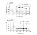
しかしながら、本出願人の研究により以下の事実が判明した。即ち、層間絶縁膜として樹脂膜を用い、ドライエッチング技術を用いてコンタクトホールを形成した場合、完成した薄膜トランジスタのしきい値電圧(Vth)が大きくばらついてしまうという事実が判明している。例えば、図4に示すデータは、SOI基板上に形成した薄膜トランジスタのしきい値電圧のばらつきについて、調べた結果である。図中の黒丸印は、層間絶縁膜として窒化シリコン膜(SiN)とアクリル膜の積層構造を用いた場合、また図中の白抜き三角印は、層間絶縁膜として窒化酸化シリコン膜(SiNO)と酸化窒化シリコン膜(SiON)の積層構造を用いた場合を示している。また、いずれの場合もコンタクトホールの開口にはドライエッチング技術を用いている。なお、「SiNO」と「SiON」の表記の違いは、前者は酸素よりも窒素を多く含み、後者は窒素よりも酸素を多く含むという意味で使い分けている。
【0006】
図4のデータは、しきい値電圧のばらつきを統計処理により評価したグラフであり、横軸にチャネル長(キャリア移動の長さ)、縦軸にVthばらつきを表している。近年、統計処理として「四分位偏差」というものが知られている。四分位偏差とは、正規確率グラフにおいて、25%の値と75%の値の差であり、異常値に影響されない統計処理として注目されている。本出願人は、この四分位偏差(25%分位偏差ともいう。)を元に、16%の値と84%の値の差を16%分位偏差と定義し、その値を「Vthばらつき」として縦軸にプロットしている。なお、16%分位偏差は、正規確率分布で言う±σに相当するため、それぞれ係数をかけて±3σと見なせる値としたものをデータプロットに用いている。同データを見る限り、層間絶縁膜にアクリル膜を用いたものは、ばらつきがnチャネル型TFTで約4倍、pチャネル型TFTで約2倍の差が出ており、明らかにアクリル膜を用いた方がばらつきが大きい。本出願人は、ドライエッチング時のプラズマダメージがアクリル膜に電荷を捕獲させ、その結果としてしきい値電圧がばらつく要因となっているのではないかと推測している。
【0007】
【発明が解決しようとする課題】
本発明は、前掲の問題に鑑みてなされたものであり、有機樹脂膜を層間絶縁膜として用いた表示装置の作製にあたって、薄膜トランジスタをそのしきい値電圧をばらつかせることなく作製する技術を提供し、表示装置の動作性能の安定性の向上及び回路設計における設計マージンの拡大を達成させることを課題とする。また、併せて表示装置の画質の向上を達成することを課題とする。
【0008】
【課題を解決するための手段】
本発明は、以下の手段により前掲の課題を解決することを特徴とするものである。即ち、有機樹脂膜として感光性有機樹脂膜(好ましくは感光性アクリル膜、特にポジ型感光性アクリル膜が望ましい。)を用い、当該感光性有機樹脂膜に第1の開口を形成した後、該第1の開口を覆う窒化絶縁膜を形成し、改めてフォトレジスト等を用いて窒化絶縁膜に第2の開口を形成し、有機樹脂膜を挟んで存在する上部電極と下部電極とを電気的に接続することを特徴とする。なお、ポジ型感光性アクリル膜を用いる場合、通常において薄茶色に着色しているため、第1の開口を設けた後、脱色処理(ブリーチング処理)を施して可視光に対して透明にしておく必要がある。脱色処理は、現像後のパターン全体に対して露光に用いた光(典型的には紫外光)を照射すれば良い。
【0009】
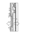
本発明について、図1を用いて説明する。図1(A)において、101は基板、102は下地膜、103はソース領域、104はドレイン領域、105はチャネル形成領域であり、これらは下地膜102上に設けられた半導体膜を用いて構成されている。また、106はゲート絶縁膜、107はゲート電極、108は第1パッシベーション膜である。ここまでは、公知の薄膜トランジスタの構造であり、各部分の材料については公知のあらゆる材料を用いることができる。
【0010】
次に、本発明の薄膜トランジスタは、無機絶縁膜である第1パッシベーション膜108上に層間絶縁膜109として感光性有機樹脂膜、特にポジ型の感光性アクリル膜を用いる点に第1の特徴がある。感光性有機樹脂膜109の膜厚は、1〜4μm(好ましくは1.5〜3μm)の範囲で選択すれば良い。そして、感光性有機樹脂膜109には第1開口部(直径φ1で表される。)110が設けられ、感光性有機樹脂膜109の上面及び前記第1開口部110の内壁面を覆うように無機絶縁膜である第2パッシベーション膜111が設けられている点が第2の特徴と言える。さらに、第2パッシベーション膜111は、前記第1開口部110の底面において、第2開口部(直径φ2で表される。)112を有しており、この第2開口部112と同じ径で前記第1パッシベーション膜108及びゲート絶縁膜106にも開口部が形成されている点が第3の特徴である。即ち、第1開口部110の内側にゲート絶縁膜106、第1パッシベーション膜108及び第2パッシベーション膜111を含む積層体に設けられた第2開口部を有する点に特徴がある。また、ソース電極113は、第1開口部110及び第2開口部112を介してソース領域103に接続され、ドレイン電極114は同様にドレイン領域104に接続される。
【0011】
なお、第1パッシベーション膜108及び第2パッシベーション膜111としては、窒化シリコン膜、窒化酸化シリコン膜、酸化窒化シリコン膜、窒化アルミニウム膜、窒化酸化アルミニウム膜もしくは酸化窒化アルミニウム膜を用いることができる。また、これらの膜を少なくとも一部に含む積層膜とすることも可能である。また、直径φ1は、2〜10μm(好ましくは3〜5μm)とし、直径φ2は、1〜5μm(好ましくは2〜3μm)とすれば良い。但し、フォトリソグラフィ工程の精度によっても開口部の直径のデザインルールは変わるため、これらの数値範囲に限定する必要はない。即ち、いずれにしてもφ1>φ2の関係を満たせば良いのである。
【0012】
ここで点線で囲まれた領域115の部分についての拡大図を図1(B)に示す。図1(B)は、第1開口部110及び第2開口部112の一部を示している。第1開口部110は、その内壁面がなだらかな曲面を形成しており、連続的に変化する曲率半径を有する。例えば、順番に3点の曲率半径R1、R2、R3に注目した時、それぞれの曲率半径の関係は、R1<R2<R3となっており、その数値は3〜30μm(代表的には10〜15μm)となっている。また、第1開口部110の底面において、感光性有機樹脂膜109と第1パッシベーション膜108のなす角(接触角θ)は、30°<θ<65°(代表的には40°<θ<50°)の範囲に収まるようにする。
【0013】
このとき、図1(B)において、116で示される部分では、第1パッシベーション膜108と第2パッシベーション膜111が密着し、感光性有機樹脂膜109を封止した状態を構成している。このとき、密着した領域、即ち第1パッシベーション膜108と第2パッシベーション膜111が接する領域の長さは、0.3〜3μm(好ましくは1〜2μm)もあれば良いが、基本的には、第1開口部110の半径が第2開口部112の半径よりも0.3〜3μmだけ大きければ良い。
【0014】
本発明で用いる感光性有機樹脂膜(ここではポジ型の感光性アクリル膜)は、薄膜トランジスタの形成中及び形成後においてもガス成分を発生させることがあるため、密着性の良い無機絶縁膜同士(特に、バリア性の高い窒化シリコン膜もしくは窒化酸化シリコン膜が好適である。)で封止しておくことは、薄膜トランジスタの上に形成する液晶素子やEL素子の劣化を防ぐという意味においても非常に重要である。
【0015】
次に、図1に示した構造を有する薄膜トランジスタの作製方法について、図2を用いて説明する。まず、図2(A)について説明する。基板101上に、下地膜102を形成し、その上に島状にエッチング加工した半導体膜を形成する。そして、その上にゲート絶縁膜106を形成し、ゲート電極107を形成し、ゲート電極107をマスクに用いて自己整合的にソース領域103及びドレイン領域104を形成する。このとき、同時にチャネル形成領域105が確定する。ソース領域103及びドレイン領域104を形成したら、加熱処理によりソース領域103及びドレイン領域104を活性化し、さらに第1パッシベーション膜108を形成した後、加熱処理により水素化処理を行う。ここまでの作製方法は公知の技術を用いて行えば良く、薄膜トランジスタを構成する材料としては、公知のあらゆる材料を用いることができる。次に、層間絶縁膜109として、感光性有機樹脂膜、ここではポジ型の感光性アクリル膜を形成する。
【0016】
次に、図2(B)について説明する。感光性有機樹脂膜109を形成したら、フォトリソグラフィ工程による露光処理を行い、感光性有機樹脂膜109をエッチングし、第1開口部110を形成する。これは感光性有機樹脂膜だから可能な技術であり、また、エッチング自体は現像液によるウェットエッチングであるため、前掲のプラズマダメージの如き問題は発生しないという効果が得られる。現像液によるエッチング後は、感光性有機樹脂膜109の脱色処理を行う。脱色処理は、露光に用いた光よりも強い光をパターン全体に照射して行えば良い。なお、脱色処理は、露光直後、即ち焼成処理の前に行う必要がある。焼成後は、感光性有機樹脂膜109の架橋が完了してしまうため、光照射による脱色が不可能だからである。
【0017】
また、第1開口部110の断面形状は、図1(B)のようになり、非常になだらかな内壁面を有する。そのため、後に形成される電極の被覆率(カバレッジ)が極めて良好なものとなる。なお、エッチング後の焼成工程においては、樹脂中への水分や酸素の吸着もしくは吸収を防ぐため、不活性雰囲気(窒素雰囲気、希ガス雰囲気もしくは水素雰囲気)で加熱することが望ましい。このとき、昇温から降温に至るまで徹底して不活性雰囲気としておくことにより、水分及び酸素の吸着(もしくは吸収)量を10ppm以下(好ましくは1ppm以下)に抑えることが望ましい。
【0018】
次に、図2(C)について説明する。第1開口部110を形成したら、感光性有機樹脂膜109の上面及び第1開口部110の内壁面を覆うように第2パッシベーション膜111を形成する。第2パッシベーション膜111は、第1パッシベーション膜108と同一の材料としても良い。第2パッシベーション膜111の形成は、高周波放電によるスパッタ法を用いることが好ましい。条件としては、シリコンターゲットを用い、スパッタガスとして窒素ガスを用いれば良い。圧力は適宜設定すれば良いが、0.5〜1.0Pa、放電電力は2.5〜3.5KW、成膜温度は室温(25℃)から250℃の範囲内とすれば良い。そして、第2パッシベーション膜111を形成したら、フォトレジスト201を形成する。このフォトレジスト201は、第2パッシベーション膜111に対して第2開口部112を形成するためのマスクである。
【0019】
次に、図2(D)について説明する。フォトレジスト201を形成したら、エッチング処理を行って第2パッシベーション膜111、第1パッシベーション膜108及びゲート絶縁膜106を順次エッチングし、第2開口部112を形成する。このとき、エッチング処理は、ドライエッチング処理でもウェットエッチング処理でも良いが、第2開口部112の形状を良好なものとするためには、ドライエッチング処理が好ましい。本発明では、ここでドライエッチング処理を行っても感光性有機樹脂膜109がプラズマに直接曝されることがないため、プラズマダメージを蓄積させてしまうような不具合が生じない。このように、感光性有機樹脂膜に設けられた開口部の内壁面を窒化シリコン膜等の窒化絶縁膜で保護しながら、その開口部の底面にさらに径の小さな開口部を設ける点が本発明の特徴の一つと言える。
【0020】
また、ドライエッチング処理により第2開口部112を形成する際、ゲート絶縁膜106及び第1パッシベーション膜108をエッチングすることになるが、このエッチングは無機絶縁膜の組み合わせによって生産性を高めることが可能である。即ち、第1パッシベーション膜108として窒化シリコン膜を用い、ゲート絶縁膜106として酸化窒化シリコン膜を用いれば、第1パッシベーション膜108のエッチングの際にはゲート絶縁膜106をエッチングストッパーとして機能させ、ゲート絶縁膜106のエッチングの際にはソース領域(シリコン膜)103をエッチングストッパーとして機能させることができる。
【0021】
例えば、ゲート絶縁膜106に酸化窒化シリコン膜、第1パッシベーション膜108に窒化シリコン膜を用いた場合を考える。第1パッシベーション膜108として機能する窒化シリコン膜は、四フッ化炭素(CF4)ガス、ヘリウム(He)ガス及び酸素(O2)ガスを用いてエッチングできるが、これらのガスはシリコン膜もエッチングしてしまう。しかしながら、下地のゲート絶縁膜106として機能する酸化窒化シリコン膜がエッチングストッパーとして働くため、ソース領域103として機能するシリコン膜を消失させてしまうことはない。また、ゲート絶縁膜(ここでは酸化窒化シリコン膜)106は、三フッ化炭化水素(CHF3)ガスを用いることでエッチングでき、かつ、シリコン膜を殆どエッチングしないので、ソース領域103をエッチングストッパーとして機能させることが可能となる。
【0022】
次に、図2(E)について説明する。第2開口部112を形成したら、その上に金属膜を形成し、エッチングによりパターン化してソース電極113及びドレイン電極114を形成する。これら電極を形成するために、チタン膜、窒化チタン膜、タングステン膜(合金を含む。)、アルミニウム膜(合金を含む。)もしくはこれらの積層膜を用いれば良い。
【0023】
以上のようにして、図1(A)、(B)で説明した構造の薄膜トランジスタを得ることができる。こうしてえた薄膜トランジスタは、感光性有機樹脂膜を有すると共に、当該感光性有機樹脂膜が平坦化膜としても機能する。また、この感光性有機樹脂膜が窒化絶縁膜(代表的には、窒化シリコン膜もしくは窒化酸化シリコン膜)に封止されているため、脱ガスによる問題も生じない。
【0024】
ここで、感光性有機樹脂膜109として、特にポジ型の感光性アクリル膜が好ましいとした理由について以下に説明する。
【0025】
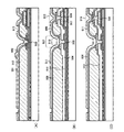
まず、図3(A)に示す写真は、非感光性アクリル膜(膜厚:約1.3μm)に対してドライエッチング処理を施してパターン化した状態の断面SEM(走査型電子顕微鏡)写真であり、図3(B)はその模式図である。従来のように非感光性アクリル膜に対してドライエッチング処理を施した場合、パターン上部に曲面は殆ど形成されず、実質的に曲率半径(R)のない上端部となる。また、パターンの下部は、テーパー角(接触角)が約63°となっているが、この下端部においても曲面は観察されない。
【0026】
次に、図5(A)に示す写真は、ポジ型感光性アクリル膜(膜厚:約2.0μm)に対して露光及び現像処理を施してパターン化した状態の断面SEM写真であり、図5(B)はその模式図である。ポジ型感光性アクリル膜の断面形状については、現像液によるエッチング処理後において非常になだらかな曲面を有し、連続的に曲率半径(R)が変化している。また、接触角も約32〜33°と小さな値が得られている。即ち、図1(B)に示した形状そのままであり、本発明の薄膜トランジスタ及び表示装置を作製するにあたって、非常に有用な形状と言える。勿論、接触角の値はエッチング条件や膜厚等によって変わるが、前掲のように30°<θ<65°を満たせば良い。
【0027】
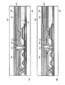
次に、図6(A)に示す写真は、ネガ型感光性アクリル膜(膜厚:約1.4μm)に対して露光及び現像処理を施してパターン化した状態の断面SEM写真であり、図6(B)はその模式図である。ネガ型感光性アクリル膜の断面形状については、現像液によるエッチング処理後においてなだらかなS字状の曲面を形成し、パターン上端部においてはある曲率半径(R)をもって湾曲している。また、接触角は約47°という値が得られている。この場合、図6(B)のWで表すテール(裾)の部分の長さが問題となる。特に、微細加工の必要なコンタクトホール(開口部)においては、このテール部分が長くなってしまうと、コンタクトホール内で下層の電極もしくは配線が露出しない状況が発生する恐れがあり、接触不良による断線が懸念される。ただし、このテール部分の長さ(W)が1μm以下(好ましくは、コンタクトホールの半径未満の長さ)であれば、そのような断線の可能性は低くなる。
【0028】
次に、図7(A)に示す写真は、ポジ型感光性ポリイミド膜(膜厚:約1.5μm)に対して露光及び現像処理を施してパターン化した状態の断面SEM写真であり、図7(B)はその模式図である。ポジ型感光性ポリイミド膜の断面形状については、現像液によるエッチング処理後において若干のテール部分(長さWで表される。)と湾曲した上端部を有しているが、その曲率半径(R)は小さい。
【0029】
以上の断面形状を観察してみると、次のような考察をすることができる。コンタクトホール(開口部)形成後、電極もしくは配線となる金属膜を成膜する際、スパッタ法、蒸着法もしくはCVD法等が用いられる。薄膜を構成する材料分子は、被形成面に付着すると安定なサイトを求めて表面を移動するが、コンタクトホールの上端部の如き鋭角をもった形状(凸部となる形状)の部分に集まりやすいことが知られている。この傾向は、特に蒸着法において顕著である。そのため、開口部の断面形状が図3(A)に示したような形状であると、開口部の縁に材料分子が集中してしまうため、その部分だけ局部的に膜厚が厚くなり、ひさし状の凸部を形成してしまう。これが後に断線(段切れ)等の不良の原因となるため、好ましいものではない。従って、図3(A)に示した非感光性アクリル膜及び図7(A)に示したポジ型感光性ポリイミド膜は、被覆率(カバレッジ)の観点から不利な材料と言える。
【0030】
また、前掲の図6(A)、図7(A)ように、コンタクトホールの下端部においてテール部分が形成されるような形状は、場合によってはテール部分がコンタクトホールの底面を覆ってしまい、接触不良を招く恐れがあるため、接触性の観点から不利な材料と言える。勿論、テール部分の長さが1μm以下(好ましくは、コンタクトホールの半径未満の長さ)であれば問題はない。
【0031】
以上の点より、本発明を実施するには図5(A)に示した形状をなすポジ型感光性アクリル膜が最も好適と言える。即ち、ポジ型感光性アクリル膜を用いれば、コンタクトホールの上端部において非常になだらかな曲面を有するため被覆率は全く問題なく、また、コンタクトホールの下端部においては、テール部分を形成せずに30°<θ<65°を満たす接触角をもって確実のコンタクトホールの底面が画定しているため、接触不良の問題も生じない。本出願人は、以上の理由により、本発明を実施するにあたって、特に有機樹脂からなる層間絶縁膜としては、ポジ型感光性アクリル膜が最も好ましい材料であると考えている。
【0032】
以上のように、有機樹脂膜を層間絶縁膜として用いた薄膜トランジスタを作製するにあたって、層間絶縁膜として感光性有機樹脂膜を用い、かつ、図1に示すコンタクト構造とすることにより、薄膜トランジスタをしきい値電圧をばらつかせることなく作製することが可能となり、薄膜トランジスタのみならずそれを用いた表示装置の動作性能の安定性の向上及び回路設計における設計マージンの拡大を達成することができる。
【0033】
【発明の実施の形態】
〔実施の形態1〕
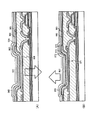
本実施の形態では、図1において、第1開口部110の形成位置を異なるものとした例について図8を用いて説明する。なお、図8(A)、(B)は、共に第2開口部まで形成した時点における断面構造を表している。また、必要に応じて図1で用いた符号を参考にする。
【0034】
図8(A)において、801は直径φ1の第1開口部であり、802は直径φ2の第2開口部である。図8(A)の特徴は、第1開口部801が、ソース領域103の端部からはみ出して設けられている点にある。感光性有機樹脂膜109は、第1パッシベーション膜108がエッチングストッパーとなってエッチングの進行が止まるため、本実施の形態の如き位置に形成することが可能である。また、図8(B)において、803は直径φ3の第1開口部であり、804は直径φ2の第2開口部である。図8(B)の特徴も、第1開口部803が、ソース領域103の側端部からはみ出して設けられている点にある。この場合もまた感光性有機樹脂膜109は、第1パッシベーション膜108がエッチングストッパーとなってエッチングの進行が止まる。
【0035】
以上のように、層間絶縁膜として用いる感光性有機樹脂膜の下にエッチングストッパーとなり得る無機絶縁膜が存在するため、第1開口部の直径を大きくとっても何ら問題はなく、コンタクトホールを形成する際の設計マージンを広くとることができるという意味で非常に有用である。
【0036】
〔実施の形態2〕
本実施の形態では、本発明をEL表示装置等の発光装置に適用した例について説明する。図9において、図9(A)は、発光装置の一画素における上面図(ただし、画素電極を形成したところまで。)であり、図9(B)はその回路図であり、図9(C)、(D)はそれぞれA−A’もしくはB−B’における断面図に相当する図面である。
【0037】
図9(A)、(B)に示すように、発光装置の表示部は、ゲート配線951、データ配線952及び電源配線(定電圧もしくは定電流を供給する配線)953で囲まれた複数の画素をマトリクス配置で有し、各画素にはスイッチング素子として機能するTFT(以下、スイッチング用TFTという。)954、EL素子を発光させるための電流もしくは電圧を供給する手段として機能するTFT(以下、駆動用TFTという。)955、容量部956及びEL素子957が設けられている。EL素子957は、ここでは図示されていなが、画素電極958の上方に発光層を設けることにより形成することができる。
【0038】
なお、本実施の形態において、スイッチング用TFT954として、マルチゲート構造のnチャネル型TFTを用い、駆動用TFT955として、pチャネル型TFTを用いているが、発光装置の画素構成はこれに限定する必要はなく、公知のどのような構成に対しても本発明を適用できる。
【0039】
図9(C)の断面図には、nチャネル型TFT954及び容量部956が現れる。901は基板であり、ガラス基板、セラミック基板、石英基板、シリコン基板もしくはプラスチック基板(プラスチックフィルムを含む。)を用いることができる。また、902は窒化酸化シリコン膜、903は酸化窒化シリコン膜であり、積層して下地膜として機能させる。勿論、これらの材料に限定する必要はない。さらに、酸化窒化シリコン膜903の上には、nチャネル型TFT954の活性層が設けられ、該活性層は、ソース領域904、ドレイン領域905、LDD領域906a〜906d及びチャネル形成領域907a、907bを有し、ソース領域904とドレイン領域905の間に、二つのチャネル形成領域及び四つのLDD領域を有している。
【0040】
また、nチャネル型TFT954の活性層は、ゲート絶縁膜908に覆われ、その上にゲート電極909a、909b及びゲート電極910a、910bが設けられている。ゲート絶縁膜908は、本実施の形態では酸化窒化シリコン膜を用いるが、比誘電率の高い窒化アルミニウム膜等の前掲の窒化絶縁膜を用いると、素子の占有面積を小さくできるため、集積度の向上に有効である。
【0041】
また、ゲート電極909a及び910aとしては、窒化タンタル膜を用い、ゲート電極909b及び910bとしては、タングステン膜を用いる。これらの金属膜は相互に選択比が高いため、エッチング条件を選択することにより図9(B)に示すような構造とすることが可能である。このエッチング条件については、本出願人による特開2001−313397号公報を参照すれば良い。
【0042】
また、ゲート電極を覆う第1パッシベーション膜911として窒化シリコン膜もしくは窒化酸化シリコン膜が設けられ、その上に感光性有機樹脂膜912(本実施の形態ではポジ型感光性アクリル膜を用いる。)が設けられる。さらに、感光性有機樹脂膜912には第1開口部(図1参照)を覆うように第2パッシベーション膜913が設けられ、第1開口部の底面において第2開口部(図1参照)が設けられる。本実施の形態では、第2パッシベーション膜913として窒化シリコン膜もしくは窒化酸化シリコン膜を用いる。勿論、窒化アルミニウム膜や窒化酸化アルミニウム膜等の他の窒化絶縁膜を用いることも可能である。
【0043】
また、データ配線952は、第2開口部を介してソース領域904に接続され、接続配線915は、第2開口部を介してドレイン領域905に接続される。接続配線915は、駆動用TFT955のゲートに接続される配線である。これらデータ配線952及び接続配線915は、アルミニウムや銅といった低抵抗な金属を主成分とする配線を他の金属膜で挟んだ構造やこれらの金属の合金膜を用いれば良い。
【0044】
また、916は駆動用TFT955のソース領域であり、電源配線953が接続される。この接続に係るコンタクト部は、本発明の実施により第1開口部及び第2開口部が形成されている。さらに電源配線953は、駆動用TFT955のゲート配線917に第1パッシベーション膜911及び第2パッシベーション膜913を介して対向すると共に保持容量956aを形成している。さらに、ゲート配線917は、半導体膜918にゲート絶縁膜908を介して対向すると共に保持容量956bを形成している。この半導体膜918は、電源配線953が半導体膜919に接続されているため、そこから電荷を供給されて電極として機能する。このように、容量部956は、保持容量956a及び956bを並列に接続した構成となるため、非常に小さな面積で大容量を得られる。さらに、特に保持容量956aは、誘電体として比誘電率の高い窒化シリコン膜を用いているため、大きな容量を確保できる。また、保持容量956aの誘電体は、第1パッシベーション膜911及び第2パッシベーション膜913の積層構造からなるため、ピンホールの発生確率が極めて低く、信頼性の高い容量を形成することができる。
【0045】
本発明を実施する場合、従来に比べて第2開口部を形成するためにフォトリソグラフィ工程で使用するマスク数が増加するが、そのマスク数の増加を逆に利用することにより、本実施の形態に示すように、新たに保持容量を形成することが可能となる。この点も本発明の大きな特徴の一つである。この本発明の特徴は、マスク増加のデメリットを補って余りあるものであり、結果的に産業の発達に大きく寄与するものである。例えば、高精細な画像表示を得るためには、表示部において各画素の面積に対する保持容量の相対的な占有面積を減らし開口率を向上させることが必要であるが、そのためには保持容量の増加は極めて有用である。
【0046】
また、図9(D)において、920は駆動用TFT955のドレイン領域であり、ドレイン配線921に接続される。そして、ドレイン配線921は、画素電極958に接続されて画素を構成する。本実施の形態では、画素電極958として可視光に対して透明な酸化物導電膜(代表的には、ITO膜)を用いるが、これに限定されない。
【0047】
以上の画素構成を有する発光装置において、実際にEL素子まで形成した例を図10に示す。図10(A)は、図9(D)に示した断面に相当する図面であり、画素電極958上に、EL素子957を形成した状態を示している。なお、図10(A)の構造とした場合、画素電極958はEL素子957の陽極に相当する。また、本明細書において、EL素子とは、陰極及び陽極の間にEL層を設け、該EL層に電圧を印加するもしくは電流を注入することにより発光させる素子を指す。
【0048】
この画素電極958の端部は、感光性有機樹脂膜961で覆われ、該感光性有機樹脂膜961は各画素を縁取るように格子状に設けられるか、又は行単位もしくは列単位でストライプ状に設けられる。いずれにしても、コンタクトホール上に形成することにより凹部を効率良く埋めることができ、全体の平坦化を兼ねることもできる。なお、本実施の形態では、感光性有機樹脂膜(第2の感光性有機樹脂膜)961として、前掲の層間絶縁膜として用いた感光性有機樹脂膜(第1の感光性有機樹脂膜)912と同一の材料(本実施の形態ではポジ型感光性アクリル膜)を用いているため、生産設備を最小限に抑えることができる。また、図示しないが、図6に示したS字状の断面形状となるネガ型感光性アクリル膜を用いても良い。勿論、このとき開口部の上端部及び下端部における曲率半径は、3〜30μm(代表的には10〜15μm)とすることが望ましい。また、その場合は、Wで示されるテール部分の長さを極力短くしないと開口率が低下してしまうため好ましくない。また、公知のレジスト材料(クロモフォアを含む高分子材料)を用いることも可能である。
【0049】
また、感光性有機樹脂膜961の表面は、第3パッシベーション膜962としての窒化絶縁膜で覆われており、これにより感光性有機樹脂膜961からの脱ガスを抑制することができる。また、画素電極958上において、第3パッシベーション膜962はエッチングされて開口部が設けられており、該開口部において、EL層963と画素電極958が接する。EL層963は、発光層、電荷注入層もしくは電荷輸送層といった薄膜を積層して構成することが一般的であるが、発光が確認されているあらゆる構造及び材料を用いることができる。例えば、電子輸送層もしくはホールブロッキング層としてシリコンを含む有機系材料であるSAlq(Alq3の3つの配位子の1つをトリフェニルシラノール構造で置換したもの)を用いることも可能である。
【0050】
勿論、有機薄膜のみで構成する必要はなく、有機薄膜と無機薄膜を積層した構造としても良いし、高分子薄膜であっても低分子薄膜であっても良い。また、成膜方法は、高分子薄膜を用いるか低分子薄膜を用いるかによって異なるが、公知の方法で成膜すれば良い。
【0051】
また、EL層963の上には、陰極964が設けられ、さらにその上には最終的に第4パッシベーション膜965としての窒化絶縁膜が設けられている。陰極964は、周期表の1族もしくは2族に属する元素を含む金属薄膜を用いれば良いが、アルミニウムに0.2〜1.5wt%(好ましくは0.5〜1.0wt%)のリチウムを添加した金属膜が電荷注入性その他の点で好適である。なお、リチウムは拡散することによってTFTの動作に害を及ぼすことが懸念されるが、本実施の形態は、第1パッシベーション911、第2パッシベーション膜913及び第3パッシベーション膜962で完全に保護されているため、リチウムの拡散は気にする必要がない。
【0052】
ここで高周波放電によるスパッタ法で形成した窒化シリコン膜のリチウムに対するブロッキング効果を示すデータを図17に示す。図17(A)は、高周波放電によるスパッタ法で形成した窒化シリコン膜(RF−SP SiNと表記)を誘電体としたMOS構造のC−V特性である。なお、「Li−dip」とは、窒化シリコン膜上にリチウムを含む溶液をスピンコートしたという意味であり、試験のため、意図的にリチウムで汚染させたことを意味する。この高周波放電によるスパッタ法で形成した窒化シリコン膜は、半径12inchの円型Siターゲットを用い、ガス流量比をN2:Ar=20:20(sccm)、成膜ガス圧力を0.8Pa、成膜電力を高周波電力で3kW、基板温度を200℃の条件にて成膜したものである。高周波放電によるスパッタ法で形成した窒化シリコン膜の組成をSIMSで測定した結果を図18及び表1に示す。図18及び表1から、窒化シリコン膜中には、水素が5×10²⁰、炭素が4×10¹⁹、酸素が2×10²¹、アルゴンが3×10²¹atoms/cm3含まれることがわかる。
【0053】
【表1】

また、図17(B)は、比較のためプラズマCVD法で形成した窒化シリコン膜(CVD SiNと表記)を誘電体としたMOS構造のC−V特性である。なお、図17(B)のデータは、金属電極としてアルミニウムにリチウムを添加した合金膜を用いている。これらに通常のBT試験を施した(具体的には、1.7MVの電圧印加に加えて±150℃で1時間の加熱処理を行った。)結果、図17(A)に示すように、高周波放電によるスパッタ法で形成した窒化シリコン膜は殆どC−V特性に変化が見られなかったのに比べ、プラズマCVD法で形成した窒化シリコン膜はC−V特性に大きな変化が見られ、リチウムによる汚染が確認された。これらのデータは、高周波放電によるスパッタ法で形成した窒化シリコン膜がリチウム拡散に対して非常に有効なブロッキング効果を有していることを示唆している。
【0055】
さらに、第2パッシベーション膜913もしくは第3パッシベーション膜962として窒化絶縁膜を用いることによって放熱効果を期待することができる。例えば、酸化シリコン膜の熱伝導率を1とすれば、窒化シリコン膜では約5、窒化アルミニウム膜では約35〜130というように非常に高い熱伝導率を有するため、EL素子が発熱した場合においても効果的に放熱が行われ、自己発熱によるEL層963の劣化を抑制することが可能である。
【0056】
なお、第3パッシベーション膜962及び第4パッシベーション膜965としては、第1パッシベーション膜911や第2パッシベーション膜913で用いた窒化絶縁膜と同じ材料を用いることが可能である。
【0057】
図10(A)に示した構造とした場合、EL素子から発した光は、画素電極958を透過して基板901側から出射される。このとき、感光性有機樹脂膜912を透過することになるため、脱色処理を十分に行って、十分に透明にしておく必要がある。
【0058】
次に、図10(B)は、画素電極958の代わりに反射性を有する金属膜971とした例であり、反射性を有する金属膜971としては、陽極として機能させるために白金(Pt)や金(Au)といった仕事関数の高い金属膜を用いる。また、これらの金属は、高価であるため、アルミニウム膜やタングステン膜といった適当な金属膜上に積層し、少なくとも最表面に白金もしくは金が露出するような画素電極としても良い。972はEL層であり、図10(A)の場合と同様に、発光が確認されているあらゆる構造及び材料を用いることができる。また、973は膜厚の薄い(好ましくは10〜50nm)金属膜であり、陰極として機能させるために周期表の1族もしくは2族に属する元素を含む金属膜を用いる。さらに、金属膜973に積層して酸化物導電膜(代表的にはITO膜)974を設け、その上に第4パッシベーション膜975を設ける。
【0059】
図10(B)に示した構造とした場合、EL素子から発した光は、画素電極971で反射され、金属膜973及び酸化物導電膜974等を透過して出射される。このとき、画素電極971の下方は光が透過することもないため、メモリ素子や抵抗素子等を設けても良いし、感光性有機樹脂膜912が着色されていても構わない。そのため、設計の自由度が高く、また製造工程を簡略化することもできるため、全体として製造コストの低減に寄与する構造と言える。
【0060】
図10(A)では、EL素子から発した光が画素電極958を透過して基板901から出射される場合(下方出射型)、図10(B)では、EL素子から発した光が画素電極971で反射され、金属膜973及び酸化物導電膜974等を透過して出射する場合(上方出射型)を示したが、EL素子から発した光が上方及び下方の両側から出射するような構造にすることもできる。この場合、例えば、図10(B)の反射性を有する金属膜971を透光性を有する酸化物導電膜(代表的にはITO膜)に置きかえて画素電極を形成すればよい。具体的な構造の例を図19に示す。図19において、981はITO膜などの酸化物導電膜で形成された画素電極、982はEL層、983は膜厚の薄い(好ましくは10〜50nm)金属膜である。金属膜983は、陰極として機能させるために周期表の1族もしくは2族に属する元素を含む金属膜を用いる。さらに、金属膜983に積層して酸化物導電膜(代表的にはITO膜)984を設け、その上に第4パッシベーション膜985を設ける。
【0061】
〔実施の形態3〕
本実施の形態では、実施の形態2に示した発光装置において、ドレイン配線921と画素電極958との接続構造を変形した例を示す。なお、基本的な構造は図9(C)と変わらないので、本実施の形態では必要箇所のみ符号を付して説明する。
【0062】
図11(A)は、酸化物導電膜を用いて画素電極501を形成した後、ドレイン配線502を形成しており、画素電極501の端部を覆うようにドレイン配線502が接触した構造となっている。この構造を形成する場合、第2開口部503を形成してから画素電極501を形成しても良いし、画素電極501を形成してから第2開口部503を形成しても良い。いずれにしても、ドライエッチング処理が行われたとしても常に感光性有機樹脂膜912は第2パッシベーション膜913によってプラズマダメージから保護されるため、薄膜トランジスタの電機特性に悪影響を与えることがない。
【0063】
次に、図11(B)は、第1パッシベーション膜911の上に無機絶縁膜でなる層間絶縁膜504を設け、その上にドレイン配線505を設けている。それと同時に、接続配線506を形成する。接続配線506は、下層の容量配線917に接続されている。これらドレイン配線505及び接続配線506は、第1開口部507を有した感光性有機樹脂膜508に覆われ、かつ、該第1開口部507は、窒化絶縁膜でなる第2パッシベーション膜509に覆われている。第2パッシベーション膜509は、第1開口部507の底面において第2開口部510を有し、第1開口部507及び第2開口部510を介して酸化物導電膜でなる画素電極511とドレイン配線505が接続される。
【0064】
このとき、接続配線506上には、第2パッシベーション膜509及び画素電極511で構成される保持容量512が形成される。図11(B)の構造とした場合、誘電体として比誘電率が高い第2パッシベーション膜509のみを用いることになるため、容量値の大きい保持容量を形成することが可能である。勿論、画素電極511と容量配線917を一対の電極として保持容量を形成することも可能であるが、その場合、誘電体として第2パッシベーション膜509、層間絶縁膜504及び第1パッシベーション膜911を用いることになるので容量値は図11(B)の構造よりも劣ってしまうことになる。
【0065】
次に、図11(C)は、図11(B)において、ドレイン配線505及び接続配線506を形成した後に別のパッシベーション膜として窒化絶縁膜513を設けた例である。こうした場合、保持容量514は、接続配線506、窒化絶縁膜513、第2パッシベーション膜509及び画素電極511で構成されることになる。この場合、図11(B)に比べて膜厚が厚くなった分、若干容量値は劣るが、誘電体を積層にすることでピンホールの問題等を低減することができ、保持容量としての信頼性を高まる。
【0066】
以上のように、本発明は、実施の形態2に示される構造に限定されるものではなく、層間絶縁膜として有機樹脂膜を用いるトランジスタ構造のすべてに適用可能である。なお、本実施の形態に示す構造において、第2パッシベーション509や窒化絶縁膜513には、前掲の実施の形態1や実施の形態2で説明した窒化絶縁膜を用いることができる。
【0067】
〔実施の形態4〕
本実施の形態では、実施の形態1〜3において、薄膜トランジスタとしてボトムゲート型の薄膜トランジスタ(具体的には、逆スタガ型TFT)を用いた例を示す。即ち、実施の形態2もしくは3において、スイッチング用TFT及び駆動用TFTとして、逆スタガ型TFTを用いても本発明を実施することができる。
【0068】
本実施の形態について、図12を用いて説明する。図12において、301は基板、302はゲート電極、303はゲート絶縁膜、304はソース領域、305はドレイン領域、306a、306bはLDD領域、307はチャネル形成領域であり、これらはゲート電極302を覆って設けられたゲート絶縁膜303上に設けられた半導体膜を用いて構成されている。また、308、309は無機絶縁膜であり、本実施の形態では、308は酸化シリコン膜であり、309は窒化シリコン膜である。309は第1パッシベーション膜として機能し、308は下層になる半導体層と窒化シリコンからなる第1パッシベーション膜309との間のバッファ層として機能する。ここまでは、公知の薄膜トランジスタの構造であり、各部分の材料については公知のあらゆる材料を用いることができる。
【0069】
次に、第1パッシベーション膜309上には、層間絶縁膜310として感光性有機樹脂膜、具体的にはポジ型感光性アクリル膜を設けられ、感光性有機樹脂膜310には第1開口部(直径φ1で表される。)311が設けられている。さらに、感光性有機樹脂膜310の上面及び前記第1開口部311の内壁面を覆うように無機絶縁膜からなる第2パッシベーション膜312が設けられ、該第2パッシベーション膜312には前記第1開口部311の底面において、第2開口部(直径φ2で表される。)313が設けられている。また、314はソース電極、315はドレイン電極である。
【0070】
本実施の形態においても、実施の形態1と同様に、第1パッシベーション膜309及び第2パッシベーション膜312としては、窒化シリコン膜、窒化酸化シリコン膜、酸化窒化シリコン膜、窒化アルミニウム膜、窒化酸化アルミニウム膜もしくは酸化窒化アルミニウム膜を用いることができる。また、これらの膜を少なくとも一部に含む積層膜とすることも可能である。また、直径φ1は、2〜10μm(好ましくは3〜5μm)とし、直径φ2は、1〜5μm(好ましくは2〜3μm)とすれば良く、φ1>φ2の関係を満たせば良い。なお、第1開口部311の断面形状については、〔課題を解決するための手段〕で詳細に説明したのでここでは省略するが、その内壁面がなだらかな曲面を形成し、連続的に変化する曲率半径を有することが望ましい。具体的には、順番に3点の曲率半径R1、R2、R3に注目した時、それぞれの曲率半径の関係は、R1<R2<R3となり、その数値は3〜30μm(代表的には10〜15μm)となることが望ましい。また、第1開口部311の底面において、感光性有機樹脂膜310と第1パッシベーション膜309のなす角(接触角θ)が30°<θ<65°(代表的には40°<θ<50°)の範囲に収まるようにすると良い。
【0071】
以上のように、本発明を実施するにあたって薄膜トランジスタの構造をトップゲート型のみもしくはボトムゲート型のみに限定する必要はなく、あらゆる構造の薄膜トランジスタに適用することができる。さらに、薄膜トランジスタに限らず、シリコンウェルを用いて形成されたMOS構造のトランジスタに適用しても良い。
【0072】
〔実施の形態5〕
本実施の形態では、本発明を液晶表示装置に適用した例について説明する。図13において、図13(A)は、液晶表示装置の一画素における上面図(ただし、画素電極を形成したところまで。)であり、図13(B)はその回路図であり、図13(C)、(D)はそれぞれA−A’もしくはB−B’における断面図に相当する図面である。
【0073】
図13(A)、(B)に示すように、液晶表示装置の表示部は、ゲート配線851、データ配線852で囲まれた複数の画素をマトリクス配置で有し、各画素にはスイッチング素子として機能するTFT(以下、スイッチング用TFTという。)853、容量部854及び液晶素子855が設けられている。図13(B)に示す回路図では、容量部854及び液晶素子855の双方が定電位線856に接続されているが、同一電位に保持する必要はなく、一方がコモン電位で他方がグラウンド電位(接地電位)であっても良い。また、ここでは図示されていないが、画素電極857の上方に液晶層を設けることにより形成することができる。なお、本実施の形態において、スイッチング用TFT853として、マルチゲート構造のnチャネル型TFTを用いているが、pチャネル型TFTを用いても良い。また、スイッチング用TFTのレイアウトは、実施者が適宜設定すれば良い。
【0074】
図13(C)の断面図には、スイッチング用TFT853及び容量部854が示されている。801は基板であり、ガラス基板、セラミック基板、石英基板、シリコン基板もしくはプラスチック基板(プラスチックフィルムを含む。)を用いることができる。また、802は窒化酸化シリコン膜、803は酸化窒化シリコン膜であり、積層して下地膜として機能させる。勿論、これらの材料に限定する必要はない。さらに、酸化窒化シリコン膜803の上には、スイッチング用TFT853の活性層が設けられ、該活性層は、ソース領域804、ドレイン領域805、LDD領域806a〜806d及びチャネル形成領域807a、807bを有し、ソース領域804とドレイン領域805の間に、二つのチャネル形成領域及び四つのLDD領域を有している。
【0075】
また、スイッチング用TFT853の活性層は、ゲート絶縁膜808に覆われ、その上にゲート電極809a、809b及びゲート電極810a、810bが設けられている。ゲート絶縁膜808は、本実施の形態では酸化窒化シリコン膜を用いる。また、ゲート電極809a及び810aとしては、窒化タンタル膜を用い、ゲート電極809b及び810bとしては、タングステン膜を用いる。これらの金属膜は相互に選択比が高いため、エッチング条件を選択することにより図13(B)に示すような構造とすることが可能である。このエッチング条件については、本出願人による特開2001−313397号公報を参照すれば良い。
【0076】
また、ゲート電極を覆う第1パッシベーション膜811として窒化シリコン膜もしくは窒化酸化シリコン膜が設けられ、その上に感光性有機樹脂膜812(本実施の形態ではポジ型感光性アクリル膜を用いる。)が設けられる。さらに、感光性有機樹脂膜812には第1開口部(図1参照)を覆うように第2パッシベーション膜813が設けられ、第1開口部の底面において第2開口部(図1参照)が設けられる。本実施の形態では、第2パッシベーション膜813として窒化シリコン膜もしくは窒化酸化シリコン膜を用いる。勿論、窒化アルミニウム膜や窒化酸化アルミニウム膜等の他の窒化絶縁膜を用いることも可能である。
【0077】
また、データ配線852は、第1開口部を介してソース領域804に接続され、ドレイン配線815は、第2開口部を介してドレイン領域805に接続される。ドレイン配線815は、容量部において保持容量を構成する電極として用いられると共に、画素電極857と電気的に接続される。なお、本実施の形態では、画素電極857として可視光に対して透明な酸化物導電膜(代表的には、ITO膜)を用いるが、これに限定されない。また、これらデータ配線852及びドレイン配線815は、アルミニウムや銅といった低抵抗な金属を主成分とする配線を他の金属膜で挟んだ構造やこれらの金属の合金膜を用いれば良い。
【0078】
ドレイン配線815は、ゲート電極と同時に形成された(即ち、ゲート電極と同一面に形成された)容量配線816に第1パッシベーション膜811及び第2パッシベーション膜813を介して対向すると共に保持容量854aを形成している。さらに、容量配線816は、半導体膜817にゲート絶縁膜808を介して対向すると共に保持容量854bを形成している。この半導体膜817は、ドレイン領域805と電気的に接続されているため、容量配線816に定電圧を印加することにより電極として機能する。このように、容量部854は、保持容量854a及び854bを並列に接続した構成となるため、非常に小さな面積で大容量を得られる。さらに、特に保持容量854aは、誘電体として、比誘電率の高い窒化シリコン膜を用いているため、大きな容量を確保できる。
【0079】
以上の画素構成を有する液晶表示装置において、実際に液晶素子まで形成した例を図14に示す。図14(A)は、図13(C)に示した断面に相当する図面であり、画素電極857上に、液晶素子855を形成した状態を示している。ドレイン配線815上には有機樹脂からなるスペーサ821が設けられ、その上から配向膜822が設けられている。スペーサ821及び配向膜822の形成順序は逆でも良い。さらに、別の基板(対向基板)823上に金属膜でなる遮光膜824、酸化物導電膜からなる対向電極825及び配向膜826を設けて、シール材(図示せず)を用いて配向膜822と配向膜826が向かい合うように貼り合わせる。さらに、シール材に設けられた液晶注入口から液晶827を注入し、液晶注入口を封止して液晶表示装置が完成する。なお、スペーサ821の形成以降の工程は、一般的な液晶のセル組み工程を適用すれば良いので、特に詳細な説明は行わない。
【0080】
図14(A)に示した構造とした場合、光は、対向基板823側から入射し、液晶827で変調されて、基板801側から出射する。このとき、透過光は、層間絶縁膜に用いた感光性有機樹脂膜812を透過することになるため、感光性有機樹脂膜812に対して脱色処理を十分に行って、十分に透明にしておく必要がある。
【0081】
次に、図14(B)は、画素電極857の代わりに反射性を有する金属膜からなるドレイン配線831をそのまま利用した例であり、反射性を有する金属膜としては、アルミニウム膜(アルミニウム合金膜を含む。)もしくは少なくとも表面に銀薄膜を有した導電膜を用いることができる。その他の図14(A)と同一の符号を付してある部分は、説明を省略する。図14(B)に示した構造とした場合、光は、対向基板823側から入射し、液晶827で変調されて、再び対向基板823側から出射する。このとき、ドレイン配線831の下方は光が透過することもないため、メモリ素子や抵抗素子等を設けても良いし、感光性有機樹脂膜812が着色されていても構わない。そのため、設計の自由度が高く、また製造工程を簡略化することもできるため、全体として製造コストの低減に寄与する構造と言える。
【0082】
〔実施の形態6〕
本実施の形態では、図9に示した発光装置の全体の構成について、図15を用いて説明する。図15は、薄膜トランジスタが形成された素子基板をシーリング材によって封止することによって形成された発光装置の上面図であり、図15(B)は、図9(A)のB−B’における断面図、図15(C)は、図15(A)のA−A’における断面図である。
【0083】
基板401上には、画素部(表示部)402、該画素部402を囲むように設けられたデータ線駆動回路403、ゲート線駆動回路404a、404b及び保護回路405が配置され、これらを囲むようにしてシール材406が設けられている。画素部402の構造については、図10及びその説明を参照すれば良い。シーリング材406としては、ガラス材、金属材(代表的にはステンレス材)、セラミックス材、プラスチック材(プラスチックフィルムも含む)を用いることができるが、図10に示したように絶縁膜のみで封止することも可能である。また、EL素子からの光の放射方向によっては、透光性材料を用いる必要がある。
【0084】
このシール材406は、データ線駆動回路403、ゲート線駆動回路404a、404b及び保護回路405の一部に重畳させて設けても良い。そして、該シール材406を用いてシーリング材407が設けられ、基板401、シール材406及びシーリング材407によって密閉空間408が形成される。シーリング材407には予め凹部の中に吸湿剤(酸化バリウムもしくは酸化カルシウム等)409が設けられ、上記密閉空間408の内部において、水分や酸素等を吸着して清浄な雰囲気に保ち、EL層の劣化を抑制する役割を果たす。この凹部は目の細かいメッシュ状のカバー材410で覆われており、該カバー材410は、空気や水分は通し、吸湿剤409は通さない。なお、密閉空間408は、窒素もしくはアルゴン等の希ガスで充填しておけばよく、不活性であれば樹脂もしくは液体で充填することも可能である。
【0085】
また、基板401上には、データ線駆動回路403及びゲート線駆動回路404a、404bに信号を伝達するための入力端子部411が設けられ、該入力端子部411へはFPC(フレキシブルプリントサーキット)412を介してビデオ信号等のデータ信号が伝達される。入力端子部411の断面は、図15(B)の通りであり、ゲート配線もしくはデータ配線と同時に形成された配線413の上に酸化物導電膜414を積層した構造の入力配線とFPC412側に設けられた配線415とを、導電体416を分散させた樹脂417を用いて電気的に接続してある。なお、導電体416としては、球状の高分子化合物に金もしくは銀といったメッキ処理を施したものを用いれば良い。
【0086】
また、図15(C)において、点線で囲まれた領域418の拡大図を図15(D)に示す。保護回路405は、薄膜トランジスタ419やコンデンサ420を組み合わせて構成すれば良く、公知の如何なる構成を用いても良い。本発明は、コンタクトホールの改善と同時に、フォトリソ工程を増加させることなく容量形成が可能である点を特徴としており、本実施の形態では、その特徴を活かしてコンデンサ420を形成しているのである。なお、薄膜トランジスタ419及びコンデンサ420の構造については、図10及びその説明を参照すれば十分に理解できるので、ここでの説明は省略する。
【0087】
本実施の形態において、保護回路405は入力端子部411とデータ線駆動回路403との間に設けられ、両者の間に突発的なパルス信号等の静電気が入った際に、該パルス信号を外部へ逃がす役割を果たす。その際、まず瞬間的に入る高電圧の信号をコンデンサ420によって鈍らせ、その他の高電圧を薄膜トランジスタや薄膜ダイオードを用いて構成した回路によって外部へと逃がすことができる。勿論、保護回路は、他の場所、例えば画素部402とデータ線駆動回路403との間や画素部402とゲート線駆動回路404a、404bの間などに設けても構わない。
【0088】
以上のように、本実施の形態では、本発明を実施するにあたって、入力端子部に設けられた静電気対策等の保護回路に用いられるコンデンサを同時形成する例を示しており、他の実施の形態1〜5のいずれの構成とも組み合わせて実施することが可能である。
【0089】
〔実施の形態7〕
本発明の表示装置を表示部に用いた電子機器として、ビデオカメラ、デジタルカメラ、ゴーグル型ディスプレイ(ヘッドマウントディスプレイ)、ナビゲーションシステム、音響再生装置(カーオーディオ、オーディオコンポ等)、ノート型パーソナルコンピュータ、ゲーム機器、携帯情報端末(モバイルコンピュータ、携帯電話、携帯型ゲーム機または電子書籍等)、記録媒体を備えた画像再生装置(具体的にはDigital Versatile Disc(DVD)等の記録媒体を再生し、その画像を表示しうるディスプレイを備えた装置)などが挙げられる。それらの電子機器の具体例を図16に示す。
【0090】
図16(A)はテレビであり、筐体2001、支持台2002、表示部2003、スピーカー部2004、ビデオ入力端子2005等を含む。本発明は表示部2003に適用することができる。なお、パソコン用、TV放送受信用、広告表示用などの全ての情報表示用のテレビが含まれる。
【0091】
図16(B)はデジタルカメラであり、本体2101、表示部2102、受像部2103、操作キー2104、外部接続ポート2105、シャッター2106等を含む。本発明は、表示部2102に適用することができる。
【0092】
図16(C)はノート型パーソナルコンピュータであり、本体2201、筐体2202、表示部2203、キーボード2204、外部接続ポート2205、ポインティングマウス2206等を含む。本発明は、表示部2203に適用することができる。
【0093】
図16(D)はモバイルコンピュータであり、本体2301、表示部2302、スイッチ2303、操作キー2304、赤外線ポート2305等を含む。本発明は、表示部2302に適用することができる。
【0094】
図16(E)は記録媒体を備えた携帯型の画像再生装置(具体的にはDVD再生装置)であり、本体2401、筐体2402、表示部A2403、表示部B2404、記録媒体(DVD等)読み込み部2405、操作キー2406、スピーカー部2407等を含む。表示部A2403は主として画像情報を表示し、表示部B2404は主として文字情報を表示するが、本発明は表示部A、B2403、2404に適用することができる。なお、記録媒体を備えた画像再生装置には家庭用ゲーム機器なども含まれる。
【0095】
図16(F)はゴーグル型ディスプレイ(ヘッドマウントディスプレイ)であり、本体2501、表示部2502、アーム部2503を含む。本発明は、表示部2502に適用することができる。
【0096】
図16(G)はビデオカメラであり、本体2601、表示部2602、筐体2603、外部接続ポート2604、リモコン受信部2605、受像部2606、バッテリー2607、音声入力部2608、操作キー2609、接眼部2610等を含む。本発明は、表示部2602に適用することができる。
【0097】
図16(H)は携帯電話であり、本体2701、筐体2702、表示部2703、音声入力部2704、音声出力部2705、操作キー2706、外部接続ポート2707、アンテナ2708等を含む。本発明は、表示部2703に適用することができる。なお、表示部2703は黒色の背景に白色の文字を表示することで携帯電話の消費電流を抑えることができる。
【0098】
以上の様に、本発明を実施して得た表示装置は、あらゆる電子機器の表示部として用いても良い。本発明により表示装置の動作性能の安定性を向上させ、かつ、回路設計における設計マージンの拡大を達成させることができるため、コストの低い表示装置を提供することができ、電子機器の部品コストを低減することができる。なお、本実施の形態の電子機器には、実施の形態1〜6に示したいずれの構成を有した表示装置を用いても良い。
【0099】
【発明の効果】
本発明により、回路設計における設計マージンの高いプロセスで、薄膜トランジスタのしきい値電圧をばらつかせることなく表示装置の作製が可能となり、表示装置の動作性能の安定性の向上を達成することができる。さらに、前掲の薄膜トランジスタを作製すると同時に、特にフォトリソ工程を増やすことなく小さな面積で大きな容量を形成することができ、表示装置の画質の向上を図ることができる。
【図面の簡単な説明】
【図1】 薄膜トランジスタの構造を示す図。
【図2】 薄膜トランジスタの作製工程を示す図。
【図3】 有機樹脂膜の断面構造を示すSEM写真及び模式図。
【図4】 しきい値電圧のバラツキを示す図。
【図5】 有機樹脂膜の断面構造を示すSEM写真及び模式図。
【図6】 有機樹脂膜の断面構造を示すSEM写真及び模式図。
【図7】 有機樹脂膜の断面構造を示すSEM写真及び模式図。
【図8】 薄膜トランジスタの構造を示す図。
【図9】 発光装置の画素構成を示す図。
【図10】 発光装置の断面構造を示す図。
【図11】 発光装置の断面構造を示す図。
【図12】 薄膜トランジスタの構造を示す図。
【図13】 液晶表示装置の画素構成を示す図。
【図14】 液晶表示装置の断面構造を示す図。
【図15】 発光装置の外観構成を示す図。
【図16】 電気器具の具体例を示す図。
【図17】 窒化シリコン膜を誘電体するMOS構造のC−V特性を示す図。
【図18】 窒化シリコン膜のSIMS測定データ。
【図19】 発光装置の断面構造を示す図。[0001]
BACKGROUND OF THE INVENTION
The present invention relates to a semiconductor element (typically a transistor) and a manufacturing method thereof, and particularly belongs to the technical field of a display device using a thin film transistor as a device. That is, a technical field related to a display device typified by a liquid crystal display device or an electroluminescence display device, a technical field related to a sensor typified by a CMOS sensor or the like, and a technical field related to any semiconductor device mounted with other semiconductor integrated circuits. Belonging to.
[0002]
[Prior art]
In recent years, development of a liquid crystal display device and an electroluminescence display device in which thin film transistors (TFTs) are integrated on a glass substrate has been advanced. In each of these display devices, a thin film transistor is formed on a glass substrate by using a thin film forming technique, and a liquid crystal element or an electroluminescence (hereinafter simply referred to as EL) element is formed on various circuits constituted by the thin film transistor. This is one of the semiconductor devices characterized in that it is formed to function as a display device.
[0003]
Since a circuit formed of a thin film transistor forms not only irregularities, flattening with an organic resin film or the like is generally performed when a liquid crystal element or an EL element is formed thereon. Each pixel provided in the display portion of the display device has a pixel electrode inside thereof, and the pixel electrode is connected to the thin film transistor through the contact hole provided in the organic resin film for planarization described above. I am doing. Such a technique is described in
[0004]
[Patent Document 1]
JP-A-10-56182 [Patent Document 2]
JP-A-10-68972 [0005]
However, the following facts have been found by the applicant's research. That is, it has been found that when a resin film is used as an interlayer insulating film and a contact hole is formed using a dry etching technique, the threshold voltage (Vth) of a completed thin film transistor varies greatly. For example, the data shown in FIG. 4 is a result of examining variation in threshold voltage of a thin film transistor formed over an SOI substrate. Black circles in the figure indicate a case where a laminated structure of a silicon nitride film (SiN) and an acrylic film is used as an interlayer insulating film, and white triangles in the figure indicate a silicon nitride oxide film (SiNO) as an interlayer insulating film. The case where a stacked structure of a silicon oxynitride film (SiON) is used is shown. In any case, a dry etching technique is used for opening the contact hole. The difference between “SiNO” and “SiON” is used in the sense that the former contains more nitrogen than oxygen and the latter contains more oxygen than nitrogen.
[0006]
The data in FIG. 4 is a graph in which the threshold voltage variation is evaluated by statistical processing. The horizontal axis represents the channel length (carrier movement length), and the vertical axis represents the Vth variation. In recent years, “quartile deviation” is known as statistical processing. The quartile deviation is a difference between a value of 25% and a value of 75% in the normal probability graph, and is attracting attention as a statistical process that is not affected by an abnormal value. Based on this quartile deviation (also referred to as 25% quartile deviation), the applicant defines the difference between the 16% value and the 84% value as the 16% quartile deviation, and the value is defined as “Vth”. The variation is plotted on the vertical axis. Since the 16% quantile corresponds to ± σ in the normal probability distribution, a value that can be regarded as ± 3σ by multiplying each coefficient is used in the data plot. As far as the same data is seen, the difference is about 4 times for the n-channel TFT and about 2 times for the p-channel TFT when the acrylic film is used for the interlayer insulating film. The variation is larger. The present applicant presumes that plasma damage during dry etching causes the acrylic film to trap charges, and as a result, the threshold voltage varies.
[0007]
[Problems to be solved by the invention]
The present invention has been made in view of the above problems, and provides a technique for manufacturing a thin film transistor without varying its threshold voltage in manufacturing a display device using an organic resin film as an interlayer insulating film. It is an object of the present invention to improve the stability of the operation performance of the display device and increase the design margin in circuit design. Another object is to improve the image quality of the display device.
[0008]
[Means for Solving the Problems]
The present invention is characterized by solving the above-mentioned problems by the following means. That is, a photosensitive organic resin film (preferably a photosensitive acrylic film, particularly a positive photosensitive acrylic film is desirable) is used as the organic resin film, and after forming the first opening in the photosensitive organic resin film, A nitride insulating film is formed to cover the first opening, and a second opening is formed again in the nitride insulating film using a photoresist or the like, and the upper electrode and the lower electrode existing between the organic resin films are electrically connected. It is characterized by connecting. When a positive photosensitive acrylic film is used, it is usually colored light brown. Therefore, after providing the first opening, a decoloring process (bleaching process) is performed to make it transparent to visible light. It is necessary to keep. The decoloring process may be performed by irradiating the entire pattern after development with light (typically ultraviolet light) used for exposure.
[0009]
The present invention will be described with reference to FIG. In FIG. 1A,
[0010]
Next, the thin film transistor of the present invention has a first feature in that a photosensitive organic resin film, particularly a positive photosensitive acrylic film is used as the
[0011]
Note that as the
[0012]
Here, an enlarged view of a
[0013]
At this time, in the portion indicated by 116 in FIG. 1B, the
[0014]
Since the photosensitive organic resin film (here, positive type photosensitive acrylic film) used in the present invention may generate a gas component during and after the formation of the thin film transistor, the inorganic insulating films having good adhesion ( In particular, sealing with a silicon nitride film or a silicon nitride oxide film having a high barrier property is also preferable in terms of preventing deterioration of a liquid crystal element or an EL element formed over the thin film transistor. is important.
[0015]
Next, a method for manufacturing a thin film transistor having the structure illustrated in FIG. 1 is described with reference to FIGS. First, FIG. 2A will be described. A
[0016]
Next, FIG. 2B will be described. After the formation of the photosensitive
[0017]
Moreover, the cross-sectional shape of the
[0018]
Next, FIG. 2C will be described. After the
[0019]
Next, FIG. 2D will be described. After the
[0020]
Further, when the
[0021]
For example, a case where a silicon oxynitride film is used for the
[0022]
Next, FIG. 2E will be described. After the
[0023]
As described above, the thin film transistor having the structure described in FIGS. 1A and 1B can be obtained. The thin film transistor thus obtained has a photosensitive organic resin film, and the photosensitive organic resin film also functions as a planarizing film. In addition, since the photosensitive organic resin film is sealed with a nitride insulating film (typically, a silicon nitride film or a silicon nitride oxide film), a problem due to degassing does not occur.
[0024]
Here, the reason why a positive photosensitive acrylic film is particularly preferable as the photosensitive
[0025]
First, the photograph shown in FIG. 3A is a cross-sectional SEM (scanning electron microscope) photograph in which a non-photosensitive acrylic film (film thickness: about 1.3 μm) is subjected to dry etching and patterned. Yes, FIG. 3B is a schematic diagram thereof. When the non-photosensitive acrylic film is dry-etched as in the prior art, a curved surface is hardly formed on the upper part of the pattern, and the upper end portion has substantially no curvature radius (R). The taper angle (contact angle) of the lower part of the pattern is about 63 °, but no curved surface is observed at the lower end.
[0026]
Next, the photograph shown in FIG. 5 (A) is a cross-sectional SEM photograph of a positive photosensitive acrylic film (film thickness: about 2.0 μm) subjected to exposure and development treatment and patterned. FIG. 5B is a schematic diagram thereof. The cross-sectional shape of the positive photosensitive acrylic film has a very gentle curved surface after etching with a developer, and the curvature radius (R) continuously changes. The contact angle is also as small as about 32 to 33 °. That is, the shape shown in FIG. 1B is maintained as it is, and can be said to be a very useful shape in manufacturing the thin film transistor and the display device of the present invention. Of course, the value of the contact angle varies depending on the etching conditions, the film thickness, etc., but it is sufficient to satisfy 30 ° <θ <65 ° as described above.
[0027]
Next, the photograph shown in FIG. 6 (A) is a cross-sectional SEM photograph in which a negative photosensitive acrylic film (film thickness: about 1.4 μm) is subjected to exposure and development treatment and patterned. 6 (B) is a schematic diagram thereof. As for the cross-sectional shape of the negative photosensitive acrylic film, a gentle S-shaped curved surface is formed after the etching process with the developer, and the upper end portion of the pattern is curved with a certain radius of curvature (R). The contact angle has a value of about 47 °. In this case, the length of the tail (hem) part represented by W in FIG. 6B becomes a problem. In particular, in a contact hole (opening) that requires fine processing, if this tail part becomes long, there is a possibility that the underlying electrode or wiring may not be exposed in the contact hole, and disconnection due to poor contact may occur. Is concerned. However, if the length (W) of the tail portion is 1 μm or less (preferably, the length is less than the radius of the contact hole), the possibility of such disconnection is reduced.
[0028]
Next, the photograph shown in FIG. 7 (A) is a cross-sectional SEM photograph in which a positive photosensitive polyimide film (film thickness: about 1.5 μm) is subjected to exposure and development treatment and patterned. FIG. 7B is a schematic diagram thereof. The cross-sectional shape of the positive photosensitive polyimide film has a slight tail portion (represented by a length W) and a curved upper end portion after the etching treatment with the developer, but the curvature radius (R ) Is small.
[0029]
When the above cross-sectional shape is observed, the following consideration can be made. After forming the contact hole (opening), a sputtering method, a vapor deposition method, a CVD method, or the like is used when forming a metal film to be an electrode or a wiring. The material molecules that make up the thin film move to the surface in search of a stable site when attached to the surface to be formed, but are likely to gather at a portion with a sharp angle (a shape that becomes a convex portion) such as the upper end of the contact hole. It is known. This tendency is particularly remarkable in the vapor deposition method. For this reason, if the cross-sectional shape of the opening is as shown in FIG. 3A, the material molecules are concentrated on the edge of the opening. Will be formed. Since this will cause defects such as disconnection (step breakage) later, it is not preferable. Therefore, the non-photosensitive acrylic film shown in FIG. 3A and the positive photosensitive polyimide film shown in FIG. 7A can be said to be disadvantageous materials from the viewpoint of coverage (coverage).
[0030]
In addition, as shown in FIGS. 6A and 7A, the shape in which the tail portion is formed at the lower end portion of the contact hole, in some cases, the tail portion covers the bottom surface of the contact hole. This may be a disadvantageous material from the viewpoint of contact because it may cause contact failure. Of course, there is no problem if the length of the tail portion is 1 μm or less (preferably, the length is less than the radius of the contact hole).
[0031]
From the above points, it can be said that the positive photosensitive acrylic film having the shape shown in FIG. In other words, if a positive photosensitive acrylic film is used, the upper end portion of the contact hole has a very gentle curved surface, so the coverage is not a problem at all, and the tail portion is not formed at the lower end portion of the contact hole. Since the bottom surface of the reliable contact hole is defined with a contact angle satisfying 30 ° <θ <65 °, the problem of poor contact does not occur. For the above reasons, the present applicant considers that a positive photosensitive acrylic film is the most preferable material particularly as an interlayer insulating film made of an organic resin, in carrying out the present invention.
[0032]
As described above, in manufacturing a thin film transistor using an organic resin film as an interlayer insulating film, the photosensitive organic resin film is used as the interlayer insulating film and the contact structure shown in FIG. It is possible to fabricate without varying the value voltage, and it is possible to improve the stability of the operation performance of not only the thin film transistor but also the display device using the thin film transistor and increase the design margin in the circuit design.
[0033]
DETAILED DESCRIPTION OF THE INVENTION
[Embodiment 1]
In this embodiment, an example in which the formation position of the
[0034]
In FIG. 8A,
[0035]
As described above, since there is an inorganic insulating film that can serve as an etching stopper under the photosensitive organic resin film used as the interlayer insulating film, there is no problem even if the diameter of the first opening is increased. It is very useful in the sense that a wide design margin can be taken.
[0036]
[Embodiment 2]
In this embodiment, an example in which the present invention is applied to a light-emitting device such as an EL display device will be described. 9A is a top view of one pixel of the light emitting device (however, up to the pixel electrode is formed), FIG. 9B is a circuit diagram thereof, and FIG. ) And (D) are drawings corresponding to cross-sectional views taken along line AA ′ or BB ′, respectively.
[0037]
As shown in FIGS. 9A and 9B, the display portion of the light-emitting device includes a plurality of pixels surrounded by a
[0038]
Note that although a multi-gate n-channel TFT is used as the switching
[0039]
In the cross-sectional view of FIG. 9C, an n-
[0040]
An active layer of the n-
[0041]
A tantalum nitride film is used as the
[0042]
In addition, a silicon nitride film or a silicon nitride oxide film is provided as the
[0043]
The
[0044]
[0045]
When practicing the present invention, the number of masks used in the photolithography process to form the second opening is increased as compared with the conventional case. By utilizing the increase in the number of masks, the present embodiment As shown in FIG. 4, it is possible to newly form a storage capacitor. This is also one of the major features of the present invention. This feature of the present invention more than compensates for the disadvantage of increasing the mask, and as a result, greatly contributes to the development of the industry. For example, in order to obtain a high-definition image display, it is necessary to reduce the relative occupied area of the storage capacitor with respect to the area of each pixel in the display unit and improve the aperture ratio. Is extremely useful.
[0046]
In FIG. 9D,
[0047]
FIG. 10 shows an example in which EL elements are actually formed in the light emitting device having the above pixel configuration. FIG. 10A is a drawing corresponding to the cross section shown in FIG. 9D and shows a state where an
[0048]
The end of the
[0049]
Further, the surface of the photosensitive
[0050]
Of course, it is not necessary to comprise only an organic thin film, a structure in which an organic thin film and an inorganic thin film are laminated, a polymer thin film, or a low molecular thin film may be used. The film forming method varies depending on whether a polymer thin film or a low molecular thin film is used, but may be formed by a known method.
[0051]
Further, a
[0052]
Here, data showing a blocking effect on lithium of a silicon nitride film formed by sputtering using high frequency discharge is shown in FIG. FIG. 17A shows CV characteristics of a MOS structure in which a silicon nitride film (referred to as RF-SP SiN) formed by sputtering using high frequency discharge is used as a dielectric. Note that “Li-dip” means that a solution containing lithium was spin-coated on a silicon nitride film, and that it was intentionally contaminated with lithium for the test. The silicon nitride film formed by this high frequency discharge sputtering method uses a circular Si target with a radius of 12 inches, the gas flow rate ratio is N 2 : Ar = 20: 20 (sccm), the film forming gas pressure is 0.8 Pa, and the composition is high. The film power is formed under the conditions of a high frequency power of 3 kW and a substrate temperature of 200 ° C. FIG. 18 and Table 1 show the results of SIMS measurement of the composition of a silicon nitride film formed by sputtering using high frequency discharge. 18 and Table 1 that the silicon nitride film contains 5 × 10 20 hydrogen, 4 × 10 19 carbon, 2 × 10 21 oxygen, and 3 × 10 21 atoms / cm 3 argon. .
[0053]
[Table 1]
FIG. 17B shows CV characteristics of a MOS structure in which a silicon nitride film (denoted as CVD SiN) formed by plasma CVD is used as a dielectric for comparison. Note that the data in FIG. 17B uses an alloy film in which lithium is added to aluminum as a metal electrode. These were subjected to a normal BT test (specifically, a heat treatment was performed at ± 150 ° C. for 1 hour in addition to a voltage application of 1.7 MV). As a result, as shown in FIG. The silicon nitride film formed by the plasma CVD method shows a significant change in the CV characteristics compared to the silicon nitride film formed by the sputtering method using the high frequency discharge, while the CV characteristics hardly change. Contamination by was confirmed. These data suggest that a silicon nitride film formed by sputtering using high frequency discharge has a very effective blocking effect against lithium diffusion.
[0055]
Further, by using a nitride insulating film as the
[0056]
Note that the
[0057]
In the case of the structure shown in FIG. 10A, light emitted from the EL element passes through the
[0058]
Next, FIG. 10B shows an example in which a
[0059]
In the case of the structure shown in FIG. 10B, light emitted from the EL element is reflected by the
[0060]
In FIG. 10A, when light emitted from the EL element is transmitted through the
[0061]
[Embodiment 3]
In this embodiment, an example in which the connection structure between the
[0062]
FIG. 11A shows a structure in which the
[0063]
Next, in FIG. 11B, an
[0064]
At this time, a
[0065]
Next, FIG. 11C illustrates an example in which the
[0066]
As described above, the present invention is not limited to the structure shown in Embodiment Mode 2, and can be applied to all transistor structures using an organic resin film as an interlayer insulating film. Note that in the structure described in this embodiment, the nitride insulating film described in
[0067]
[Embodiment 4]
In this embodiment, an example in which a bottom-gate thin film transistor (specifically, an inverted staggered TFT) is used as the thin film transistor in
[0068]
This embodiment will be described with reference to FIG. In FIG. 12, 301 is a substrate, 302 is a gate electrode, 303 is a gate insulating film, 304 is a source region, 305 is a drain region, 306a and 306b are LDD regions, and 307 is a channel formation region. A semiconductor film provided over the
[0069]
Next, a photosensitive organic resin film, specifically a positive photosensitive acrylic film, is provided as an
[0070]
Also in this embodiment mode, as in
[0071]
As described above, it is not necessary to limit the structure of a thin film transistor to only a top gate type or only a bottom gate type in practicing the present invention, and the present invention can be applied to thin film transistors having any structure. Further, the present invention is not limited to a thin film transistor, and may be applied to a MOS transistor formed using a silicon well.
[0072]
[Embodiment 5]
In this embodiment, an example in which the present invention is applied to a liquid crystal display device will be described. 13A is a top view of one pixel of a liquid crystal display device (however, up to the point where a pixel electrode is formed), FIG. 13B is a circuit diagram thereof, and FIG. C) and (D) are drawings corresponding to cross-sectional views taken along the line AA ′ or BB ′, respectively.
[0073]
As shown in FIGS. 13A and 13B, the display portion of the liquid crystal display device includes a plurality of pixels surrounded by a
[0074]
In the cross-sectional view of FIG. 13C, a switching
[0075]
The active layer of the switching
[0076]
In addition, a silicon nitride film or a silicon nitride oxide film is provided as the
[0077]
The
[0078]
The
[0079]
FIG. 14 shows an example in which liquid crystal elements are actually formed in the liquid crystal display device having the above pixel configuration. FIG. 14A is a drawing corresponding to the cross section shown in FIG. 13C and shows a state in which a
[0080]
In the case of the structure shown in FIG. 14A, light is incident from the
[0081]
Next, FIG. 14B shows an example in which a
[0082]
[Embodiment 6]
In this embodiment, the entire structure of the light-emitting device illustrated in FIG. 9 will be described with reference to FIG. FIG. 15 is a top view of a light-emitting device formed by sealing an element substrate on which a thin film transistor is formed with a sealing material, and FIG. 15B is a cross-sectional view taken along line BB ′ in FIG. FIG. 15C is a cross-sectional view taken along the line AA ′ of FIG.
[0083]
On the
[0084]
The
[0085]
An
[0086]
Further, in FIG. 15C, an enlarged view of a
[0087]
In this embodiment mode, the
[0088]
As described above, in this embodiment, an example in which a capacitor used in a protection circuit such as a countermeasure against static electricity provided in an input terminal portion is simultaneously formed in implementing the present invention is shown. It can be implemented in combination with any of the
[0089]
[Embodiment 7]
As an electronic device using the display device of the present invention as a display unit, a video camera, a digital camera, a goggle type display (head mounted display), a navigation system, an audio playback device (car audio, audio component, etc.), a notebook type personal computer, Reproducing a recording medium such as a game machine, a portable information terminal (mobile computer, cellular phone, portable game machine or electronic book), an image reproducing apparatus (specifically, a digital versatile disc (DVD)) provided with a recording medium, And a device provided with a display capable of displaying the image). Specific examples of these electronic devices are shown in FIGS.
[0090]
FIG. 16A illustrates a television which includes a
[0091]
FIG. 16B illustrates a digital camera, which includes a
[0092]
FIG. 16C illustrates a laptop personal computer, which includes a
[0093]
FIG. 16D illustrates a mobile computer, which includes a
[0094]
FIG. 16E illustrates a portable image reproducing device (specifically, a DVD reproducing device) provided with a recording medium, which includes a
[0095]
FIG. 16F illustrates a goggle type display (head mounted display), which includes a
[0096]
FIG. 16G illustrates a video camera, which includes a main body 2601, a display portion 2602, a
[0097]
FIG. 16H illustrates a mobile phone, which includes a
[0098]
As described above, the display device obtained by implementing the present invention may be used as a display unit of any electronic device. According to the present invention, the stability of the operation performance of the display device can be improved and the design margin can be expanded in the circuit design. Therefore, a low-cost display device can be provided, and the component cost of the electronic equipment can be reduced. Can be reduced. Note that a display device having any of the structures described in
[0099]
【The invention's effect】
According to the present invention, a display device can be manufactured through a process with a high design margin in circuit design without varying the threshold voltage of a thin film transistor, and the stability of operation performance of the display device can be improved. . Furthermore, at the same time as the above-described thin film transistor is manufactured, a large capacity can be formed with a small area without increasing the number of photolithography processes, and the image quality of the display device can be improved.
[Brief description of the drawings]
FIG. 1 illustrates a structure of a thin film transistor.
FIGS. 2A and 2B illustrate a manufacturing process of a thin film transistor. FIGS.
FIGS. 3A and 3B are an SEM photograph and a schematic view showing a cross-sectional structure of an organic resin film. FIGS.
FIG. 4 is a diagram showing variations in threshold voltage.
FIGS. 5A and 5B are an SEM photograph and a schematic view showing a cross-sectional structure of an organic resin film. FIGS.
6A and 6B are a SEM photograph and a schematic view showing a cross-sectional structure of an organic resin film.
7A and 7B are a SEM photograph and a schematic view showing a cross-sectional structure of an organic resin film.
FIG. 8 illustrates a structure of a thin film transistor.
FIG 9 illustrates a pixel structure of a light-emitting device.
FIG 10 illustrates a cross-sectional structure of a light-emitting device.
FIG 11 illustrates a cross-sectional structure of a light-emitting device.
FIG. 12 illustrates a structure of a thin film transistor.
FIG. 13 illustrates a pixel structure of a liquid crystal display device.
FIG 14 illustrates a cross-sectional structure of a liquid crystal display device.
FIG 15 illustrates an external structure of a light-emitting device.
FIG. 16 is a diagram showing a specific example of an electric appliance.
FIG. 17 is a diagram showing CV characteristics of a MOS structure in which a silicon nitride film is dielectric.
FIG. 18 shows SIMS measurement data of a silicon nitride film.
FIG 19 illustrates a cross-sectional structure of a light-emitting device.
Claims (15)
前記薄膜トランジスタの上に設けられた第1窒化絶縁膜と、
前記第1窒化絶縁膜の上に設けられたポジ型感光性アクリル膜と、
前記ポジ型感光性アクリル膜の上に設けられた第2窒化絶縁膜と、
前記第2窒化絶縁膜の上に設けられた電極または配線とを有し、
前記ポジ型感光性アクリル膜に設けられた第1開口部の内壁面が前記第2窒化絶縁膜に覆われており、
前記第1開口部の底面において前記第1窒化絶縁膜と前記第2窒化絶縁膜が接する領域を有し、
前記第1開口部の内側に、前記第1窒化絶縁膜及び前記第2窒化絶縁膜に設けられた第2開口部を有し、
前記第2開口部を介して前記薄膜トランジスタを構成する島状の半導体膜と前記電極または前記配線とが電気的に接続され、
前記ポジ型感光性アクリル膜の表面の曲率半径は、前記第1開口部から離れるに従って連続的に長くなっていることを特徴とする半導体装置。A thin film transistor;
A first nitride insulating film provided on the thin film transistor;
A positive photosensitive acrylic film provided on the first nitride insulating film;
A second nitride insulating film provided on the positive photosensitive acrylic film ;
An electrode or a wiring provided on the second nitride insulating film;
An inner wall surface of a first opening provided in the positive photosensitive acrylic film is covered with the second nitride insulating film;
A region where the first nitride insulating film and the second nitride insulating film are in contact with each other at the bottom surface of the first opening;
A second opening provided in the first nitride insulating film and the second nitride insulating film inside the first opening;
The island-shaped semiconductor film constituting the thin film transistor and the electrode or the wiring are electrically connected through the second opening ,
The semiconductor device according to claim 1, wherein a radius of curvature of the surface of the positive photosensitive acrylic film is continuously increased as the distance from the first opening is increased .
前記薄膜トランジスタの上に設けられた第1窒化絶縁膜と、
前記第1窒化絶縁膜の上に設けられたポジ型感光性アクリル膜と、
前記ポジ型感光性アクリル膜の上に設けられた第2窒化絶縁膜と、
前記第2窒化絶縁膜の上に設けられた電極または配線とを有し、
前記ポジ型感光性アクリル膜に設けられた第1開口部の内壁面が前記第2窒化絶縁膜に覆われており、
前記第1開口部の底面において前記第1窒化絶縁膜と前記第2窒化絶縁膜が接する領域を有し、
前記第1開口部の内側に、前記第1窒化絶縁膜及び前記第2窒化絶縁膜に設けられた第2開口部を有し、
前記第2開口部を介して前記薄膜トランジスタを構成する島状の半導体膜と前記電極または前記配線とが電気的に接続され、
前記ポジ型感光性アクリル膜の表面の曲率半径は、3〜30μmの範囲内で連続的に変化しており、前記第1開口部から離れるに従って連続的に長くなっていることを特徴とする半導体装置。A thin film transistor;
A first nitride insulating film provided on the thin film transistor;
A positive photosensitive acrylic film provided on the first nitride insulating film;
A second nitride insulating film provided on the positive photosensitive acrylic film ;
An electrode or a wiring provided on the second nitride insulating film;
An inner wall surface of a first opening provided in the positive photosensitive acrylic film is covered with the second nitride insulating film;
A region where the first nitride insulating film and the second nitride insulating film are in contact with each other at the bottom surface of the first opening;
A second opening provided in the first nitride insulating film and the second nitride insulating film inside the first opening;
The island-shaped semiconductor film constituting the thin film transistor and the electrode or the wiring are electrically connected through the second opening ,
The semiconductor substrate is characterized in that the radius of curvature of the surface of the positive photosensitive acrylic film continuously changes within a range of 3 to 30 μm, and continuously increases as the distance from the first opening portion increases. apparatus.
前記EL素子は、Liが添加された金属膜を一方の電極として有することを特徴とする半導体装置。The EL element includes a metal film to which Li is added as one electrode.
前記EL素子は、前記第2窒化絶縁膜の上に設けられ、前記電極または前記配線に電気的に接続された画素電極を有し、The EL element has a pixel electrode provided on the second nitride insulating film and electrically connected to the electrode or the wiring,
前記画素電極の端部は感光性有機樹脂膜で覆われており、The edge of the pixel electrode is covered with a photosensitive organic resin film,
前記感光性有機樹脂膜の表面は第3窒化絶縁膜で覆われていることを特徴とする半導体装置。A semiconductor device, wherein the surface of the photosensitive organic resin film is covered with a third nitride insulating film.
前記第1開口部の下端部における接触角(θ)は、30°<θ<65°を満たすことを特徴とする半導体装置。In any one of Claims 1 thru | or 6 ,
A contact angle (θ) at a lower end portion of the first opening satisfies 30 ° <θ <65 °.
前記第1開口部の直径φ1と、前記第2開口部の直径φ2とは、φ1>φ2の関係を満たすことを特徴とする半導体装置。In any one of Claims 1 thru | or 7 ,
The diameter φ1 of the first opening and the diameter φ2 of the second opening satisfy a relationship of φ1> φ2.
前記第1窒化絶縁膜上にポジ型感光性アクリル膜を形成し、
前記ポジ型感光性アクリル膜に露光及び現像処理を施して、前記ポジ型感光性アクリル膜に前記第1窒化絶縁膜の一部を露出する第1開口部を形成し、
前記ポジ型感光性アクリル膜の上面及び前記第1開口部の内壁面を覆うように第2窒化絶縁膜を形成し、
前記第1窒化絶縁膜、及び前記第2窒化絶縁膜をエッチングして、前記第1開口部の内側に第2開口部を形成し、
前記第2開口部を介して前記薄膜トランジスタを構成する島状の半導体膜と電気的に接続する電極または配線を形成し、
前記ポジ型感光性アクリル膜の表面の曲率半径は、前記第1開口部から離れるに従って連続的に長くなっていることを特徴とする半導体装置の作製方法。Forming a first nitride insulating film so as to cover the thin film transistor;
Forming a positive photosensitive acrylic film on the first nitride insulating film;
The positive photosensitive acrylic film is exposed and developed to form a first opening that exposes a portion of the first nitride insulating film in the positive photosensitive acrylic film ;
Forming a second nitride insulating film so as to cover the upper surface of the positive photosensitive acrylic film and the inner wall surface of the first opening;
Etching the first nitride insulating film and the second nitride insulating film to form a second opening inside the first opening,
Forming an electrode or wiring electrically connected to the island-shaped semiconductor film constituting the thin film transistor through the second opening ;
A method of manufacturing a semiconductor device , wherein a radius of curvature of the surface of the positive photosensitive acrylic film is continuously increased as the distance from the first opening is increased .
前記ポジ型感光性アクリル膜に前記第1開口部を形成した後に焼成処理を行い、A baking treatment is performed after forming the first opening in the positive photosensitive acrylic film,
前記第1開口部を形成した後、前記焼成処理の前に、記ポジ型感光性アクリル膜の脱色処理を行うことを特徴とする半導体装置の作製方法。A method for manufacturing a semiconductor device, wherein after the first opening is formed and before the baking treatment, the positive photosensitive acrylic film is decolored.
前記第1開口部の下端部における接触角(θ)は、30°<θ<65°を満たすことを特徴とする半導体装置の作製方法。A method for manufacturing a semiconductor device, wherein a contact angle (θ) at a lower end portion of the first opening satisfies 30 ° <θ <65 °.
前記第1開口部の直径φ1と、前記第2開口部の直径φ2とは、φ1>φ2の関係を満たすことを特徴とする半導体装置の作製方法。In any one of Claims 11 thru | or 14 ,
A method for manufacturing a semiconductor device, wherein a diameter φ1 of the first opening and a diameter φ2 of the second opening satisfy a relationship of φ1> φ2.
Priority Applications (1)
| Application Number | Priority Date | Filing Date | Title |
|---|---|---|---|
| JP2003105028A JP4409196B2 (en) | 2002-04-09 | 2003-04-09 | Semiconductor device, display device using the same, and method for manufacturing the semiconductor device |
Applications Claiming Priority (2)
| Application Number | Priority Date | Filing Date | Title |
|---|---|---|---|
| JP2002107197 | 2002-04-09 | ||
| JP2003105028A JP4409196B2 (en) | 2002-04-09 | 2003-04-09 | Semiconductor device, display device using the same, and method for manufacturing the semiconductor device |
Related Child Applications (2)
| Application Number | Title | Priority Date | Filing Date |
|---|---|---|---|
| JP2009140919A Division JP4515528B2 (en) | 2002-04-09 | 2009-06-12 | Semiconductor device |
| JP2009239128A Division JP4652470B2 (en) | 2002-04-09 | 2009-10-16 | Display device |
Publications (3)
| Publication Number | Publication Date |
|---|---|
| JP2004006796A JP2004006796A (en) | 2004-01-08 |
| JP2004006796A5 JP2004006796A5 (en) | 2007-09-20 |
| JP4409196B2 true JP4409196B2 (en) | 2010-02-03 |
Family
ID=30446816
Family Applications (1)
| Application Number | Title | Priority Date | Filing Date |
|---|---|---|---|
| JP2003105028A Expired - Fee Related JP4409196B2 (en) | 2002-04-09 | 2003-04-09 | Semiconductor device, display device using the same, and method for manufacturing the semiconductor device |
Country Status (1)
| Country | Link |
|---|---|
| JP (1) | JP4409196B2 (en) |
Families Citing this family (8)
| Publication number | Priority date | Publication date | Assignee | Title |
|---|---|---|---|---|
| US7977678B2 (en) * | 2007-12-21 | 2011-07-12 | Semiconductor Energy Laboratory Co., Ltd. | Semiconductor display device |
| WO2013073084A1 (en) * | 2011-11-16 | 2013-05-23 | パナソニック株式会社 | Method for producing display panels, and display panel |
| CN107564967B (en) | 2012-07-20 | 2020-10-23 | 株式会社半导体能源研究所 | Display device |
| JP6367655B2 (en) * | 2013-09-13 | 2018-08-01 | 株式会社半導体エネルギー研究所 | Method for manufacturing semiconductor device |
| TWI553388B (en) * | 2014-09-11 | 2016-10-11 | 群創光電股份有限公司 | Liquid crystal display and element substrate thereof |
| CN104597640B (en) * | 2015-02-12 | 2017-06-27 | 深圳市华星光电技术有限公司 | Array base palte and its method for repairing disconnected lines |
| CN116154003A (en) | 2015-11-20 | 2023-05-23 | 株式会社半导体能源研究所 | Semiconductor device, display device including the same, and electronic apparatus including the same |
| KR20220119606A (en) * | 2019-12-27 | 2022-08-30 | 가부시키가이샤 한도오따이 에네루기 켄큐쇼 | Semiconductor device and method of manufacturing semiconductor device |
-
2003
- 2003-04-09 JP JP2003105028A patent/JP4409196B2/en not_active Expired - Fee Related
Also Published As
| Publication number | Publication date |
|---|---|
| JP2004006796A (en) | 2004-01-08 |
Similar Documents
| Publication | Publication Date | Title |
|---|---|---|
| JP4652470B2 (en) | Display device | |
| JP4463493B2 (en) | Display device and manufacturing method thereof | |
| JP4409196B2 (en) | Semiconductor device, display device using the same, and method for manufacturing the semiconductor device |
Legal Events
| Date | Code | Title | Description |
|---|---|---|---|
| A521 | Request for written amendment filed |
Free format text: JAPANESE INTERMEDIATE CODE: A523 Effective date: 20060407 |
|
| A621 | Written request for application examination |
Free format text: JAPANESE INTERMEDIATE CODE: A621 Effective date: 20060407 |
|
| A521 | Request for written amendment filed |
Free format text: JAPANESE INTERMEDIATE CODE: A523 Effective date: 20070627 |
|
| A521 | Request for written amendment filed |
Free format text: JAPANESE INTERMEDIATE CODE: A523 Effective date: 20070808 |
|
| A977 | Report on retrieval |
Free format text: JAPANESE INTERMEDIATE CODE: A971007 Effective date: 20090803 |
|
| A131 | Notification of reasons for refusal |
Free format text: JAPANESE INTERMEDIATE CODE: A131 Effective date: 20090818 |
|
| A521 | Request for written amendment filed |
Free format text: JAPANESE INTERMEDIATE CODE: A523 Effective date: 20091015 |
|
| TRDD | Decision of grant or rejection written | ||
| A01 | Written decision to grant a patent or to grant a registration (utility model) |
Free format text: JAPANESE INTERMEDIATE CODE: A01 Effective date: 20091110 |
|
| A01 | Written decision to grant a patent or to grant a registration (utility model) |
Free format text: JAPANESE INTERMEDIATE CODE: A01 |
|
| A61 | First payment of annual fees (during grant procedure) |
Free format text: JAPANESE INTERMEDIATE CODE: A61 Effective date: 20091111 |
|
| R150 | Certificate of patent or registration of utility model |
Ref document number: 4409196 Country of ref document: JP Free format text: JAPANESE INTERMEDIATE CODE: R150 Free format text: JAPANESE INTERMEDIATE CODE: R150 |
|
| FPAY | Renewal fee payment (event date is renewal date of database) |
Free format text: PAYMENT UNTIL: 20121120 Year of fee payment: 3 |
|
| FPAY | Renewal fee payment (event date is renewal date of database) |
Free format text: PAYMENT UNTIL: 20121120 Year of fee payment: 3 |
|
| FPAY | Renewal fee payment (event date is renewal date of database) |
Free format text: PAYMENT UNTIL: 20121120 Year of fee payment: 3 |
|
| FPAY | Renewal fee payment (event date is renewal date of database) |
Free format text: PAYMENT UNTIL: 20131120 Year of fee payment: 4 |
|
| R250 | Receipt of annual fees |
Free format text: JAPANESE INTERMEDIATE CODE: R250 |
|
| R250 | Receipt of annual fees |
Free format text: JAPANESE INTERMEDIATE CODE: R250 |
|
| R250 | Receipt of annual fees |
Free format text: JAPANESE INTERMEDIATE CODE: R250 |
|
| R250 | Receipt of annual fees |
Free format text: JAPANESE INTERMEDIATE CODE: R250 |
|
| R250 | Receipt of annual fees |
Free format text: JAPANESE INTERMEDIATE CODE: R250 |
|
| R250 | Receipt of annual fees |
Free format text: JAPANESE INTERMEDIATE CODE: R250 |
|
| R250 | Receipt of annual fees |
Free format text: JAPANESE INTERMEDIATE CODE: R250 |
|
| R250 | Receipt of annual fees |
Free format text: JAPANESE INTERMEDIATE CODE: R250 |
|
| R250 | Receipt of annual fees |
Free format text: JAPANESE INTERMEDIATE CODE: R250 |
|
| R250 | Receipt of annual fees |
Free format text: JAPANESE INTERMEDIATE CODE: R250 |
|
| LAPS | Cancellation because of no payment of annual fees |