JP4408514B2 - Image forming apparatus - Google Patents
Image forming apparatus Download PDFInfo
- Publication number
- JP4408514B2 JP4408514B2 JP2000025315A JP2000025315A JP4408514B2 JP 4408514 B2 JP4408514 B2 JP 4408514B2 JP 2000025315 A JP2000025315 A JP 2000025315A JP 2000025315 A JP2000025315 A JP 2000025315A JP 4408514 B2 JP4408514 B2 JP 4408514B2
- Authority
- JP
- Japan
- Prior art keywords
- image
- charging
- color
- image forming
- transfer
- Prior art date
- Legal status (The legal status is an assumption and is not a legal conclusion. Google has not performed a legal analysis and makes no representation as to the accuracy of the status listed.)
- Expired - Fee Related
Links
Images


Description
【0001】
【発明の属する技術分野】
本発明は、像担持体に形成された静電潜像を現像剤により現像し、得られた画像を転写材に転写する画像形成ユニットを複数持ち、多色画像を出力することができる画像形成装置に関する。
【0002】
【従来の技術】
従来の多色画像形成を行う画像形成装置について簡単に説明する。
【0003】
近年、書類のカラー化にともない、図9のような複数の画像形成ユニットを備えたカラー複写機が考案されている。
【0004】
複数の現像手段を備えた単一の画像形成ユニットによる画像形成装置では、ユニットの感光ドラムを色数だけ回転しなければならず、カラー画像の出力速度を高くすることができないのに対し、この複数ユニットの画像形成装置では、単色の場合と同様の出力速度を維持できる利点がある。以下、その動作について説明する。
【0005】
図9において、まず、原稿台100上に原稿Gを複写すべき面を下側にしてセットし、つぎにコピーボタンを押すことにより複写が開始される。原稿照明用ランプ、短焦点レンズアレイ、CCDセンサーが一体のユニット9になって、原稿を照射しながら走査することにより、その照明走査光の原稿面反射光が、短焦点レンズアレイによって結像されてCCDセンサーに入射される。CCDセンサーによって得られた画像情報のアナログ信号は、周知の画像処理を行ってデジタル信号に変換され、プリンター部に送られる。
【0006】
プリンター部においては、上記の画像信号を受けて以下のようにして、各ユニットの感光ドラム1に静電潜像を形成する。感光ドラム1は、中心支軸を中心に所定の周速度で回転駆動され、その回転過程で帯電器3により正極性または負極性の一様帯電処理を受け、その一様帯電面に、画像信号に対応してON、OFF発光されるレーザー露光装置2の固体レーザー素子の光を高速で回転する回転多面鏡によって走査することにより、感光ドラム1の表面に原稿画像に対応した静電潜像が順次形成されていく。つぎに、この静電潜像をトナーと磁性キャリアとを有する2成分現像剤を収容した現像器4により現像し、感光ドラム1上にトナー像を形成する。
【0007】
プリンター部におけるこのような動作は、各色について同時に行うために、レーザースキャナーおよび画像形成ユニットを各色ごとに具備しており、感光ドラム1上に同時にトナー像を形成し、転写ベルト15によって搬送されてくる転写材に、転写帯電器7により重ね合わせて多重転写することにより、転写材上に多色画像を得ることができる。その後、転写材を転写ベルト15から静電分離して定着器6へ送り、そこでトナー像を熱定着して、フルカラーの画像として出力される。
【0008】
一方、トナー像転写後の感光ドラム1の表面は、クリーナ5によって転写残りトナー等の付着汚染物を除去し、必要に応じて像露光の光メモリを前露光手段8による露光によって除去してから、感光ドラム1が繰り返し画像形成に使用される。
【0009】
上記のような電子写真画像形成装置に用いられる感光ドラム1としては、有機感光体やアモルファスシリコン系感光体(a−Si系感光体)等がよく用いられる。このうち、有機感光体はカラー、白黒を問わず、複写機やプリンターなどで用いられるが、a−Si系感光体は、表面硬度が高く、半導体レーザーなどに高い感度を示し、しかも繰り返し使用による劣化もほとんど認められないことから、モノクロの高速複写機やレーザビームプリンタ(LBP)などの電子写真用感光体として用いられているが、カラー電子写真画像形成装置ではまだ製品化されていない。
【0010】
【発明が解決しようとする課題】
前記のように、a−Si系感光体がカラー電子写真画像形成装置で用いられない理由は様々であるが、一つの要因は、電位ムラが有機感光体に比べて発生しやすいため、カラーバランスやハーフトーン濃度等において条件が厳しいカラー画像形成装置では、採用されなかったということである。
【0011】
上記の電位ムラが発生する原因の一つに、a−Si系感光体の製造方法によるものがある。a−Si感光体は、原料ガスを高周波やマイクロ波でプラズマ化し、固体化して、アルミニウム等のシリンダー上に堆積し、感光層を成膜するため、プラズマが均一でないと、周方向に膜厚のムラが発生し、現像部において周方向に20V程度の電位ムラが発生してしまっていた。これは、膜厚のムラにより静電容量の違いができ、感光層の帯電能の差やトナーによる現像量の差が生じるのと、前の画像形成での光メモリーを消すために行った前露光により帯電−現像間で起こる電位減衰が、膜厚に差があると差が生じて、現像部における電位ムラをより増大させることにより発生する。
【0012】
上記の帯電後の電位減衰は、a−Si系感光体の場合、有機感光体に比べて暗部状態でも非常に大きく、さらに像露光の光メモリーによる電位減衰が増大するため、前の画像形成での光メモリーを消すための前露光が帯電前に必要となる。このため、帯電位置−現像位置間での電位減衰は非常に大きくなり、100〜200V程度の電位減衰が生じる。このとき上述の膜厚ムラにより、感光体の周方向上で10〜20V程度の電位ムラが発生してしまっていた。
【0013】
このような電位ムラが生じると、静電容量の大きなa−Si系感光体は有機感光体に比べて、コントラストも小さいためより影響を受けてしまい、濃度ムラも顕著になる。
【0014】
このように、電位ムラがある感光体を複数の画像形成ユニットを持つ画像形成装置に用いると、各色の感光ドラムごとにムラが生じるため、たとえばグレーのハーフトーンを出力すると、転写材上の搬送方向(感光ドラムの周方向と同方向)に沿う位置で混色状態が変わり、それにともない色味がずれてしまっていた。
【0015】
白黒画像の場合の濃度ムラも問題ではあるが、白黒画像の場合はハーフトーンをあまり取らないことや色情報がないため、電位ムラはある程度許容されていたが、カラー画像では、ハーフトーンを使うことが多いことに加え、色味のずれは濃度ずれよりも許容されるレベルが厳しいため、20V程度の電位ムラでも問題となっていた。
【0016】
本発明の目的は、複数の画像形成ユニットの各感光体に周方向に電位ムラがあっても、電位ムラによる濃度ムラを制御することにより、転写材上に色味変動を最小限にした多色画像を得ることができる画像形成装置を提供することである。
【0017】
【課題を解決するための手段】
上記目的は本発明に係る画像形成装置にて達成される。要約すれば、本発明は、各々がアモルファスシリコンを含む感光体と、帯電手段と、像露光手段と、現像手段と、転写手段とを有するイエロー、マゼンタ、シアン、ブラックの4色の画像形成ユニットを備え、前記各画像形成ユニットの各感光体に対する帯電、像露光および現像、および得られたトナー像の転写材への転写によって、前記転写材に複数色のトナー像を重ねた多色画像を形成する画像形成装置において、
前記各感光体の周方向上の状態に関する位置情報として、感光体の未像露光時の現像位置における帯電電位に関する位置情報を有し、前記各感光体間において、前記イエロー、マゼンタ、シアン用の3色の感光体については、前記感光体1周期における前記帯電電位が最大値もしくは最小値になる部分が、前記転写材上において一致するように、前記転写材の転写位置と前記感光体の周方向上位置の関係を制御し、前記ブラック用の感光体については、前記感光体1周期における前記帯電電位が最大値もしくは最小値になる部分が、前記3色の感光体と逆になるように、前記転写材の転写位置と前記感光体の周方向上位置の関係を制御することを特徴とする画像形成装置である。
【0019】
また、前記帯電器が、磁気ブラシ帯電器もしくは帯電ローラに導電性粒子を塗布した帯電器とすることができる。画像形成装置は、前記トナー像を前記転写材に転写する前に、一旦転写する中間転写体を備えることができ、前記転写材の転写位置と前記感光体の周方向上位置の関係の代わりに、前記中間転写体の転写位置と前記感光体の周方向上位置の関係を制御する。
【0020】
【発明の実施の形態】
以下、本発明に係る実施例を図面に則して更に詳しく説明する。
【0021】
実施例1
図1は、本発明の画像形成装置の一実施例を示す断面図である。
【0022】
本画像形成装置は、転写材搬送手段である転写ベルト15に沿ってイエロー(Y)、マゼンタ(M)、シアン(C)の画像形成ユニットを具備し、3色フルカラー画像を形成することが可能に構成されている。
【0023】
本実施例では、各画像形成ユニットの感光ドラム(ドラム型感光体)10にはa−Si系感光体を用いた。これについては後述する。
【0024】
感光ドラム10の帯電にはコロナ帯電器方式を用いた。感光ドラム10表面の帯電は、コロナ帯電器3の一次ワイヤーに5〜6kV程度を印加し、一次ワイヤー電流を1mAに定電流制御して行った。帯電電位は帯電器3のグリッドバイアスによって制御した。
【0025】
この帯電された各感光ドラム10の表面に、潜像形成手段であるレーザー露光装置2によってイメージ露光を施し、各色の静電潜像を書き込んだ。ついで各色の静電潜像をそれぞれの現像器4により現像して、イエロー、マゼンタ、シアンのトナー像として可視化し、ついで転写ベルト15に担持して搬送されてくる図示しない転写材に、転写帯電器7により重ね合わせて転写した。その後、転写材を定着器6へ搬送し、トナー像を熱定着して画像を出力した。
【0026】
トナー像転写後の各感光ドラム10の表面には、転写残りトナーが残留している。転写残りトナーはクリーニング手段5のクリーニングブレードによって掻き取られ、クリーニング手段5の容器内に収容される。ついで感光ドラム10は、像露光による光メモリーを前露光手段8による前露光で除去した後、繰り返し画像形成に使用される。本実施例では、前露光手段8から発する前露光の波長を680nmとした。
【0027】
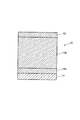
図2は、本発明で感光ドラム10として用いた帯電特性が正極性のa−Si(アモルファスシリコン)系感光体の層構成を模式的に示す断面図である。
【0028】
このa−Si系感光体は、Alなどの円筒状の導電性支持体(シリンダー)11の表面上に、感光層12および表面層13をこの順で形成して構成されている。感光層12は、電荷注入阻止層12aと光導電層12bとからなっている。電荷注入阻止層12aは、導電性支持体11から光導電層12bへの電荷の注入を阻止するためのもので、必要に応じて設けられる。光導電層12bは、少なくともシリコンを含む非晶質材料で構成され、光導電性を示す。表面層13は、シリコンと炭素(必要により、水素もしくはハロゲンまたはその両者)を含み、電子写真装置における潜像を保持する能力を有する。
【0029】
a−Si系感光体は、従来例のところで述べたように、原料ガスを高周波やマイクロ波でプラズマ化し、固体化して、アルミニウム等のシリンダー上に堆積し、感光層を成膜しているので、プラズマが均一でないと、周方向に膜厚のムラが発生して、従来、現像部において感光体に周方向に20V程度の電位ムラが発生してしまっていた。これは、膜厚のムラにより静電容量の違いができ、感光層の帯電能に差が生じるのと、前の画像形成での光メモリーを消すために行った前露光により帯電−現像間で起こる電位減衰が、膜厚に差があると差が生じて、現像部における電位ムラをより増大させることにより発生する。
【0030】
上記の光メモリーについて説明すると、a−Si系感光体を帯電し、像露光を行うと、光キャリアが生成し、感光体の表面電位が減衰する。このとき、a−Si系感光体は、多くのタングリングボンド(未結合手)を有しており、これが局在準位となって光キャリアの一部を捕捉し、光キャリアの走行性を低下させ、あるいは光キャリアの再結合確率を低下させる。したがって、像露光により生成された光キャリアの一部は、つぎの画像形成工程での帯電時にa−Si系感光体に電界がかかると、同時に局在準位から開放されて、a−Si系感光体の表面電位に前の画像形成工程での露光部と非露光部とで差が生じ、これが最終的に光メモリーとなる。
【0031】
そこで、前露光工程において均一露光を行って、a−Si系感光体内部に潜在する光キャリアを過多にして、全面で均一になるようにすることにより、光メモリーを消去することが一般的である。このとき、前露光手段8から発する前露光の光量を増やしたり、前露光の波長をa−Si系感光体の分光感度ピーク(約680〜700nm)に近づけることで、より効果的に光メモリー(ゴースト)を消去することが可能である。
【0032】
しかしながら、上記のようにa−Si系感光体に膜厚ムラが存在すると、光導電層間にかかる電界が異なるため、局在準位からの光キャリアの開放に差が生じ、膜厚が薄い部分ほど電位減衰が大きくなる。このため、帯電部でたとえ均一に帯電できたとしても、現像部では電位ムラが生じてしまう。また帯電能についても、膜厚が薄い部分ほど静電容量が大きくなるため不利となり、帯電能が低下してくると、現像部での帯電ムラがより顕著になる。
【0033】
この膜厚ムラによる電位ムラは、図3に示すように、a−Si系感光ドラムの1周期内で最大値、最小値を対極位置に持つことが多い。これは、プラズマ分布によるものであり、感光層の製造方法によって異なる。製法によっては、1周期中に数個のピークが現れたりする場合もある。
【0034】
本実施例では、図3のようなパターンの電位ムラを生じる膜厚ムラを有する感光体を代表例に取り上げて、それに対処する制御方法を以下説明するが、本発明は、これに限定されるわけではない。
【0035】
まず最初に、各画像形成ユニットのa−Si系感光ドラム10の周方向現像位置に図示しない表面電位計を設置し、感光ドラムを回転しながら現像位置で周方向の電位ムラを各色ごとに測定して、感光ドラム10の周方向上の電位ムラに関する位置情報を求める。
【0036】
測定時には、現像工程は行わずに帯電工程および前露光工程のみを行い、周方向位置における電位測定情報から、各感光ドラムの電位が最大になる部分と最小になる部分を特定する。
【0037】
一方、感光ドラム10に取り付けられている回転駆動用のギアフランジは、前述の測定において得られた電位の最大値および最小値が検出可能な状態で取り付けられている。これに係合した回転駆動軸との関係から、各色の感光ドラムは、各色のユニット間の距離を考慮して転写材上において、各色の感光ドラムの電位の最大値および最小値が重なるように調整して取り付けられる。
【0038】
また感光ドラムの駆動は各ステーションごとに各々のモータを持つ独立駆動の場合でも、1モータで全てのステーションを駆動する場合でも、いずれでもかまわない。ただし、各々のモータで独立駆動する場合には、駆動軸(感光ドラム)の回転方向の位置を検出する手段を設けるなどして駆動を制御する必要があり、また、1モータで全てのステーションを駆動する場合には、各々のステーションの駆動ギア等の精度を管理し、連続使用により各々のステーションの感光ドラムの位置関係が変わらないように設置する必要がある。また転写材上において各色の感光ドラムの電位の最大値か最小値が重なるようにするためには、各ステーション間の感光ドラム間距離は感光ドラムの周長の整数倍である方向が好ましいが、感光ドラムの回転方向の位置関係さえ制御されていれば、感光ドラム間距離についても特に制限はない。
【0039】
このとき感光ドラム10の電位ムラの大きさは、各色の間でレベル差があっても本発明の効果は得られるが、望ましくは各色で電位ムラの極大値、極小値が同程度の感光ドラムを用いることが好ましい。
【0040】
本実施例によれば、電位ムラの位置制御方法は、上記の電位ムラに関する位置情報に基づき、感光ドラム10を周方向に移動し、要すれば2つ以上の感光ドラムを周方向に移動して、各感光ドラム10間で電位ムラの周方向位置と転写材上の転写位置とが一致するように、つまり、現像位置での未像露光部電位の感光ドラム1周期中における最大値もしくは最小値となる部分が、転写材上において各色で一致するように、感光ドラムの周方向位置を調整することからなる。
【0041】
本実施例において、上記各色の感光ドラムの電位ムラの周方向位置関係が転写材上で一致するように、電位ムラの位置制御を行って、グレーの全面ハーフトーンチャートを画像形成し、出力した画像の色ムラを評価した。比較のために、感光ドラムを不規則に取り付けたまま、電位ムラの位置制御を行わずに感光ドラムを使用して、同様に画像形成を行った。
【0042】
評価は、イエロー、マゼンタ、シアンの重ね合わせにより生成されるグレー画像で反射濃度が約0.3になる条件のチャートを用い、転写材搬送方向に等間隔で画像上に採った10点の側定点で、L*A*B*空間の色度値を測定し、各点間の色差(色度差)δの最大値で行った。ここで、測定装置としては、Gretag Macbeth社のSpectrolinoを用いて測定を行っている。
【0043】
その結果、比較例の場合には、出力画像は色差δの最大値が10以上になったが、本実施例では、出力画像の色差δの最大値を5以内に収めることができた。
【0044】
これは、各色の感光ドラムの電位ムラの位置制御を行わずに画像出力した場合には、1枚の画像中で各色のムラの位置が違うので、各点における混色状態が変わり、それにともない色味がずれてしまったからである。これに対し、本実施例のように、電位ムラの位置制御によって、各色の感光ドラムの電位ムラの周方向位置関係が転写材上で一致するようにした場合には、1枚の画像中で各色のムラの位置が一致するので、濃度のムラは発生するものの、その混色比率はほぼ均一化され、その結果、色味の変動を最小限に抑えることができるからである。
【0045】
実施例2
図4は、本発明の画像形成装置の他の実施例を示す断面図である。
【0046】
実施例1では帯電手段としてコロナ帯電器を用いたが、本実施例では、磁性粒子による磁気ブラシ帯電器20を用いたことが特徴である。本実施例のその他の構成は実施例1と基本的に同じで、図4において図1に付した符号と同一の符号は同一の部材を示す。
【0047】
a−Si系の感光体の帯電手段としては従来からコロナ帯電器が実用化されているが、a−Si系感光体は、比誘電率が11〜12と有機感光体に比べて大きいため、静電容量が大きくなり、それにともない帯電能の低下、放電による潜像の流れでの画像流れ等が発生しやすくなる。
【0048】
これに対し、帯電部材として導電性ローラやファーブラシローラ、磁性粒子を担持したマグネットローラ等を用いた接触帯電手段は、a−Si系感光体を帯電すると、a−Si系感光体表面が109〜1014Ωcmの材質の層により形成されていることから、接触帯電部材に印加した帯電バイアスのうち直流成分とほぼ同等の帯電電位を感光体表面に得ることが可能である。
【0049】
このような帯電方法は、放電を用いずに、電荷を直接感光体に注入して帯電を行うため、注入帯電と称されている。この注入帯電によれば、感光体への帯電がコロナ帯電器による帯電のときのような放電現象を利用しないので、完全なオゾンレスかつ停電電力消費型の帯電が可能となり、近年、富みに注目されてきている。また帯電能の低下や画像流れが防止できるとともに、印加した電圧近傍に帯電されるために、帯電電位の制御も容易になる。
【0050】
磁気ブラシ帯電器20は、導電性の磁性粒子をマグネットを内包した支持スリーブ上に磁気的に拘束して、磁性粒子に磁気ブラシを形成させ、その磁気ブラシをスリーブの回転によって回転しながら感光体に接触して、スリーブに電圧を印加することによって帯電を開始するものである。
【0051】
図5に、本実施例で用いた磁気ブラシ帯電器の断面図を示す。磁気ブラシ帯電器20は、下端が開口したケーシング25内に、固定マグネットローラ21を非回転に内包した外径16mmの非磁性の支持スリーブ22を回転自在に設置し、このスリーブ22の外周面にマグネットローラ21の磁力で磁性粒子23を付着保持してなっている。スリーブ22の回転により磁性粒子23を感光ドラム10に向けて搬送し、規制ブレード24により層厚を規制された磁性粒子23に、マグネットローラ21の磁界により磁気ブラシを形成させ、感光ドラム10に接触させる。
【0052】
本実施例では、磁性粒子23の磁気ブラシが感光ドラム10と接触するニップ幅を約6mmに調整した。またスリーブ22は感光ドラム10に対しカウンター方向に回転し、その回転速度を感光ドラム10の回転速度100mm/秒に対し150mm/秒とした。支持スリーブ22に帯電バイアスを印加すると、スリーブ22上の磁性粒子23から感光ドラム10の表面に電荷が注入され、感光ドラム10の表面が帯電バイアスの直流成分に近い帯電電位に帯電される。
【0053】
磁性粒子23としては、一般に、平均粒径10〜100μm、飽和磁化20〜250emu/cm3、抵抗102〜1010Ωcmのものが好ましく、感光ドラム10にピンホールのような絶縁欠陥が存在することを考慮すると、抵抗が106Ωcm以上のものを用いることが好ましい。磁性粒子の抵抗値は、底面積が228cm2の金属セルに磁性粒子を2g入れた後、6.6kg/cm2で加重し、100Vの電圧を印加して測定した。
【0054】
また、磁気ブラシの帯電性能を良くするためには、できるだけ抵抗の小さい磁性粒子を用いる方がよく、本例では、平均粒径25μm、飽和磁化200emu/cm3、抵抗5×106Ωcmの磁性粒子を用いた。この磁性粒子は、フェライト表面を酸化・還元処理して、抵抗調整を行ったものである。
【0055】
本実施例において、実施例1と同様に、各画像形成ユニットのa−Si系感光ドラム10の周方向現像位置に図示しない表面電位計を設置し、感光ドラムを回転しながら現像位置で周方向の電位ムラを各色ごとに測定して、感光ドラム10の周方向上の電位ムラに関する位置情報を求め、得られた周方向現像位置における電位測定情報から、各感光ドラムの電位が最大になる部分と最小になる部分を特定する。
【0056】
また、感光ドラム10に取り付けられている回転駆動用のギアフランジは、前述の測定において得られた電位の最大値および最小値が検出可能な状態で取り付けられており、これに係合した回転駆動軸との関係から、各色の感光ドラムは、各色のユニット間の距離を考慮して転写材上において、各色の感光ドラムの電位の最大値および最小値が重なるように調整して取り付けられる。
【0057】
本実施例において、実施例1と同様に、電位ムラの位置制御を行って、グレーの全面ハーフトーンチャートを画像形成し、出力した画像の色ムラを評価した。比較例として、実施例1のときと同様、電位ムラに対する位置制御を行わない場合にも画像形成を行った。
【0058】
評価方法も実施例1と同様で、イエロー、マゼンタ、シアンの重ね合わせにより生成されるグレー画像で反射濃度が約0.3になる条件のチャートを用い、転写材搬送方向に等間隔で画像上に採った10点の側定点で、L*A*B*空間の色度値を測定し、各点間の色差(色度差)δの最大値で行った。
【0059】
その結果、各色の感光ドラムの電位ムラの位置関係の制御を行わずに、3色フルカラーの画像出力した比較例では、色差δの最大値が10以上であったのが、本実施例では、各色の感光ドラムの電位ムラの周方向位置関係が転写材上で一致するように制御を行って、画像出力したので、画像の色差δの最大値を5以内に収めることができた。
【0060】
本発明は、このように、磁気ブラシ帯電器を用いてa−Si系の各色の感光ドラムを帯電する画像形成装置においても適用することができ、同様に優れた効果を奏する。
【0061】
実施例3
図6は、本発明の画像形成装置の他の実施例を示す断面図、図7は、図6の画像形成装置で用いた帯電器を示す断面図である。
【0062】
実施例1では帯電手段としてコロナ帯電器を用い、実施例2では磁気ブラシ帯電器を用いたが、本実施例では、図7に示すような接触帯電器30を用いた。本実施例のその他の構成は実施例1と基本的に同じで、図6において図1に付した符号と同一の符号は同一の部材を示す。
【0063】
帯電器30は、下端が一部開口したケーシング34内に帯電ローラ31を回転自在に配置し、粒子塗布手段32で帯電ローラ31に帯電促進粒子33を塗布し、帯電促進粒子33を塗布した帯電ローラ31を感光ドラム10の表面に接触し、帯電ローラ31に印加した帯電バイアスにより、感光ドラム10の表面を帯電するものである。
【0064】
帯電ローラ31は、芯金上に弾性発泡体の中抵抗層を設けてなっており、本実施例では、中抵抗層を、たとえばウレタンのような樹脂、たとえばカーボンブラックのような導電性粒子、および硫化剤、発泡剤等から材料を処方して、芯金上にローラ状に形成した。その後必要に応じて中抵抗層の表面を研磨して、帯電ローラ31を直径12mmの弾性導電性ローラとして作成した。
【0065】
このように作成された帯電ローラ31のローラ抵抗は、100kΩが測定された。測定は、帯電ローラ両端に突出した芯金に総圧1kgの荷重がかかるようにして、帯電ローラを外径30mmのアルミニウムドラムに圧着し、この状態で芯金とアルミニウムドラムの間に100Vを印加して行った。
【0066】
帯電ローラ31は電極として機能することが重要である。つまり、帯電ローラ31に弾性を持ち、被帯電体である感光ドラム10と十分な接触状態を得ることができるだけでなく、移動する感光ドラム10を充電(電荷注入)により帯電するのに足る十分に低い抵抗を有することが必要である。一方、感光ドラム10にピンホールなどの欠陥部位が存在した場合に電圧のリークを防止する必要がある。これらから、帯電ローラ31に十分な帯電性と耐リーク性を得るには、104〜107Ωの抵抗を有することが好ましい。
【0067】
帯電ローラ31の中抵抗層の材質としては、弾性発泡体に限定されるものではなく、EPDMやウレタン、シリコーンゴム、IR等の弾性材料に、抵抗調整のためにカーボンブラックや金属酸化物等の導電性物質を分散したゴム材が挙げられる。特に導電性物質を分散させずに、イオン導電性の材料を用いて抵抗調整することも可能である。
【0068】
上記のような帯電ローラ31をa−Si系感光ドラム10に当接し、電圧を印加することにより帯電が可能であるが、本実施例のように、帯電ローラ31の表面に帯電促進粒子33を塗布すると、感光ドラム10との接触性の向上と摩擦力の低下がより大きく得られる。帯電ローラ31と感光ドラム10の接触ニップには、帯電促進粒子33が介在した状態で感光ドラム10の帯電が行われる。
【0069】
これにより、帯電ローラ31が感光ドラム10と速度差を持って接触できると同時に、帯電促進粒子33を介して密に感光ドラム10に電荷を注入でき、帯電ローラ31のみの場合よりも高い充電効率が得られ、帯電ローラ31に印加した直流電圧とほぼ同等の電位を感光ドラム10に与えることができる。
【0070】
本実施例では、帯電促進粒子33として比抵抗が106Ωcm、平均粒径が3μmの導電性酸化亜鉛粒子を用いた。
【0071】
帯電促進粒子33の材料としては、金属酸化物などの導電性無機粒子やこれと有機物粒子との混合物等、各種の導電性粒子が使用可能である。帯電促進粒子の抵抗は、粒子を介して電荷の授受を行うため、比抵抗で1010Ωcm以下が好ましい。帯電促進粒子の比抵抗の測定は錠剤法によっており、底面積2.26cm2の円筒内に約0.5gの帯電促進粒子を入れ、円筒の上下の電極を15kgで加圧した状態で100Vの電圧を印加して、ペレット状の粒子の抵抗値を測定し、その抵抗値を正規化して比抵抗値を求めた。
【0072】
帯電促進粒子33の平均粒径は、良好な均一帯電を得るために50μm以下が好ましい。平均粒径の下限値は、粒子が安定して得られるものとして、10nmが限界である。本発明において、粒子が凝集体として構成されている場合の粒径は、その凝集体の平均粒径として定義した。粒径の測定には、光学顕微鏡あるいは電子顕微鏡による観察から、粒子を100個以上抽出し、水平方向最大弦長をもって体積粒度分布を算出し、その50%平均粒径をもって決定した。
【0073】
上記の粒子塗布手段32は、帯電ローラ31に当接して回転するローラ32aに対して固形化された帯電促進粒子33をバネ32bによって加圧当接し、ローラ32aに対し摺擦させることにより微量ずつ塗布する構成をとっており、さらにこのようにしてローラ32aの表面に付着した帯電促進粒子33を帯電ローラ31上に均一に塗布し、帯電ローラ31により感光ドラム10との接触ニップ(帯電ニップ)に帯電促進粒子33を均一に供給させるためのものである。
【0074】
本実施例では、帯電ローラ31を感光ドラム10に対し速度差を持って回転させている。このため、弾性体からなる帯電ローラ31の接触ニップ近傍は従来と比べて大きく変形し、帯電ローラ31の表面に付着している帯電促進粒子は感光ドラム10に移行しやすく、使用につれて帯電ローラ31表面の帯電促進粒子は減少する。帯電ローラ31上の帯電促進粒子33の減少は、塗布手段32による帯電促進粒子33の塗布により補われる。
【0075】
本実施例における帯電装置30の動作について説明すると、まず、帯電ローラ31の表面に粒子塗布手段32により帯電促進粒子33を塗布する。塗布された帯電促進粒子は、帯電ローラ31の回転により感光ドラム10と対向した帯電部(接触ニップ)に搬送される。帯電ローラ31は、当接部が感光ドラム10と逆方向に移動する向きに等速度で駆動されており、帯電ローラ31の芯金に帯電バイアスを印加する。帯電ローラ31と感光ドラム10の接触ニップにおいて、感光ドラム10の表面を隙間なく摺擦する帯電促進粒子33を介してa−Si系感光ドラム10の表面に電荷が注入され、感光ドラム10の表面が印加電圧とほぼ等しい電位に帯電される。
【0076】
本実施例において、これまでの実施例と同様、表面電位計により現像位置で各感光ドラム10の周方向の電位ムラを測定し、感光ドラムの回転駆動用のギアフランジとその回転駆動軸との関係から、各感光ドラムの電位ムラの周方向位置関係が転写材上で一致するように、感光ドラムの周方向位置を調整して制御した。そして3色フルカラーの画像を形成し、出力した画像の色ムラを評価した。比較のために、電位ムラの位置制御を行わずに感光ドラムを使用して、同様に画像形成を行った。評価法は、同様に、転写材搬送方向に等間隔で画像上に採った10点の側定点で、L*A*B*空間の色度値を測定し、各点間の色差(色度差)δの最大値による判定である。
【0077】
その結果、各色の感光ドラムの電位ムラの位置関係の制御を行わずに、3色フルカラーの画像出力した比較例では、色差δの最大値が10以上であったのが、本実施例では、各色の感光ドラムの電位ムラの周方向位置関係が転写材上で一致するように制御を行って、画像出力したので、画像の色差δの最大値を5以内に収めることができた。
【0078】
本発明は、このように、帯電促進粒子と帯電ローラを組み合わせた接触帯電器を用いてa−Si系の各色の感光ドラムを帯電する画像形成装置においても適用することができ、同様に優れた効果を奏する。
【0079】
実施例4
図8は、本発明の画像形成装置のさらに他の実施例を示す断面図である。
【0080】
実施例1〜3では、イエロー、マゼンタ、シアンの3色の画像形成ユニットを具備し、3色フルカラーの画像形成を行う画像形成装置に適用した場合を説明したが、本発明は、図8に示すように、イエロー(Y)、マゼンタ(M)、シアン(C)、ブラック(K)の4色の画像形成ユニットを備え、4色フルカラーの画像形成を行う画像形成装置にも適用することができる。図8において、図1に付した符号と同一の符号は同一の部材を示す。
【0081】
このような4色フルカラーの画像形成装置は、画像形成装置がデジタル方式になってからカラー画像形成装置の主流となっている。ブラックのユニットを持つ利点は、黒文字のシャープ化、UCR(Under Colar Removal)による色トナーの低減などが挙げられる。
【0082】
UCRは、現在、ブラックの現像剤を用いているフルカラー画像形成装置においては一般的に使用されている技術であり、イエロー、マゼンタ、シアンをブラックに置き換えて、黒の再現性を高めるとともに、トナー量の低減を図るものである。イエロー、マゼンタ、シアン、ブラックの共通部分をすべてブラックに置き換えるのを100%UCRといい、共通部分の50%をブラックに置き換えるのを50%UCRという。現状の一般的なフルカラー画像形成装置では100%UCRを行わず、イエロー、マゼンタ、シアンとブラックとを用いてブラックやグレーを再現している。
【0083】
本実施例では、上記のUCRを用いてa−Si系感光ドラム10の帯電ムラに起因する色味変動の低減とともに、濃度変動の低減も実現できる方法を用いた。
【0084】
具体的には、イエロー、マゼンタ、シアンの感光ドラム10については、実施例1〜3と同様、現像位置での未像露光部電位の感光ドラム1周期中における最大値もしくは最小値の部分が、転写材上において各色について一致するように、感光ドラムの位置関係を制御し、ブラックの感光ドラムについては上記の周期の逆になるように、すなわちブラックの最小値、最大値になる位置が、イエロー、マゼンタ、シアンの最大値、最小値に当たる部分とが転写材上において一致するように制御した。
【0085】
このように、ブラックのユニットの場合、電位ムラを逆に重ねてやることにより、たとえばグレーを50%UCRで画像を出力すると、イエロー、マゼンタ、シアンの3色で作るグレーと、ブラックで作るグレーとがほぼ同等となり、濃度ムラを低減できる。また色味についてはイエロー、マゼンタ、シアンの3色の組み合わせバランスをできるだけ均一化することにより、かなり改善できる。
【0086】
本実施例において、上記3色の感光ドラムの電位ムラの位置関係が転写材上で一致するように制御し、ブラックの感光ドラムについては電位ムラの位置関係が逆周期(逆位相)となるように制御を行った下で、4色フルカラーの画像を形成し、出力した画像の色ムラを評価した。比較のために、感光ドラムの電位ムラの位置関係の制御を行わずに、同様に画像形成を行った。これまでと同様、転写材搬送方向に等間隔で画像上に採った10点の側定点で、L*A*B*空間の色度値を測定し、各点間の色差(色度差)δの最大値により、画像を評価した。
【0087】
その結果、イエロー、マゼンタ、シアン、ブラックの4色の感光ドラムについて、電位ムラの位置関係の制御を行わずに画像を出力した比較例の場合には、色差δの最大値が10以上であったのが、本実施例のように、3色の感光ドラムの電位ムラの位置関係を制御し、ブラックの感光ドラムについては電位ムラの位置関係を逆周期となるように制御を行って、画像を出力した場合には、色差δの最大値を5以内に収めることができ、かつ濃度ムラもほとんど認識できないレベルまで低減することが可能となった。
【0088】
これは、各色の感光ドラムの位置関係の電位ムラの位置制御を行わずに画像出力した場合には、1枚の画像中で各色のムラの位置が違うため、各点における混色状態が変わり、それにともない色味がずれてしまったからである。これに対し、本実施例では、イエロー、マゼンタ、シアンの各色の感光ドラムの電位ムラの周方向位置関係が転写材上で一致するように調整して画像出力したので、各色のムラの位置が一致し、その混色比率はほぼ均一化されるため、色味の変動を最小限に抑えることができ、またブラックについては電位ムラを逆周期で重ねて画像出力したので、3色のときの濃度ムラを打ち消すことができ、濃度ムラも軽減することができたためである。
【0089】
以上の実施例では、帯電手段として、コロナ帯電器、磁気ブラシ帯電器、帯電ローラに帯電促進粒子を組み合わせた帯電器を用いた場合について説明した。
【0090】
好ましくは、実施例2、3で用いたような磁気ブラシ帯電器、帯電ローラに帯電促進粒子を組み合わせた帯電器のように、a−Si系感光体に対して十分な接触点を持ち、電荷を直接感光体に注入して帯電を行う注入帯電方式を用いることが望ましい。この注入帯電を用いれば、感光体への帯電がコロナ帯電器を用いて行われるような放電現象を利用しないので、完全なオゾンレスかつ低電力消費型帯電が可能となる。また、帯電能の低下や画像流れが防止できるとともに、印加した電圧近傍に帯電されるため、電位の制御を行うことも容易となる。また、本発明の課題となっている光メモリーの影響に対しても、注入帯電を用いた方が改善されることが確認されており、前記の電位ムラも改善される傾向にある。
【0091】
ただし、本発明は、実施例1で用いたコロナ帯電器の場合でも十分な効果が得られており、注入帯電を用いた場合に限られるものではなく、その他にも、たとえばローラ帯電器、ファーブラシ帯電器等を使用した場合にも、本発明の効果に影響はなく、十分な効果を得ることができる。
【0092】
また感光体はポジ帯電のa−Si系感光ドラムについて述べたが、ネガ帯電のa−Si系感光ドラムを用いることもでき、同様の効果が得られることが確認されている。つまり、感光ドラムの帯電極性や層構成によらず、a−Si系感光ドラムで周方向の帯電ムラが発生する場合には、本発明を適用することができ、十分な効果を発揮する。
【0093】
周方向の帯電ムラの要因も、実施例中では、感光層の膜厚ムラを例に説明したが、膜の特性やドラム基体等の下地の影響などでも、帯電ムラが発生することがある。本発明は、帯電ムラが周方向にあるa−Si系感光体を用いた画像形成ユニットを複数備えた全ての場合に適用することができ、周方向帯電ムラの要因の如何を問わない。
【0094】
以上の実施例では、いずれも、転写ベルトに沿って複数の画像形成ユニットを配置し、それらの感光体上の各色のトナー像を記録材に直接転写する方式の画像形成装置について説明したが、本発明はこれに限られず、中間転写体(中間転写ベルト)に沿って複数の画像形成ユニットを配置し、それらの感光体上の各色のトナー像を中間転写体に重ね合わせて転写し(1次転写)、ついで中間転写体に送られた記録材に重ね合わせた各色のトナー像を一括して転写する(2次転写)方式の画像形成装置についても適用することができる。この場合、転写材の転写位置と感光体の周方向上位置の関係の代わりに、中間転写体の転写位置と感光体の周方向上位置の関係を制御すればよく、同様な効果を奏することができる。
【0095】
【発明の効果】
以上説明したように、本発明によれば、イエロー、マゼンタ、シアンの画像形成ユニットの各々に設置されたアモルファスシリコンを含む感光体について、感光体の未像露光時の現像位置における帯電電位に関する位置情報を有し、各感光体間において、現像位置での帯電電位の感光体1周期中における最大値もしくは最小値になる部分が、転写材(中間転写体があるときはその中間転写体)上において一致するように、転写材(中間転写体)の転写位置と感光体の周方向上位置の関係を制御するようにしたので、各感光体に周方向に電位ムラがあっても、転写材上に色味変動を最小限にした多色画像を得ることができる。また画像形成ユニットがイエロー、マゼンタ、シアン、ブラックの4色分設置されている場合には、イエロー、マゼンタ、シアン用の3色の感光体については、上記と同様に制御し、ブラック用の感光体については、現像位置での帯電電位の感光体1周期中における最大値もしくは最小値になる部分が、3色の感光体と逆になるように、転写材(中間転写体)の転写位置と感光体の周方向上位置の関係を制御するようにしたので、色味変動とともに濃度ムラも最小限にした多色画像を得ることができる。
【図面の簡単な説明】
【図1】本発明の画像形成装置の一実施例を示す断面図である。
【図2】本発明で使用したa−Si系感光体の層構成を示す断面図である。
【図3】a−Si系感光ドラムの帯電電位のムラを示す電位図である。
【図4】本発明の画像形成装置の他の実施例を示す断面図である。
【図5】図4の画像形成装置で用いた磁気ブラシ帯電器を示す断面図である。
【図6】本発明の画像形成装置のさらに他の実施例を示す断面図である。
【図7】図6の画像形成装置で用いた帯電ローラに帯電促進粒子を組み合わせた帯電器を示す断面図である。
【図8】本発明の画像形成装置のさらに他の実施例を示す断面図である。
【図9】従来の画像形成装置を示す断面図である。
【符号の説明】
2 レーザー露光装置
3 コロナ帯電器
4 現像器
7 転写帯電器
8 前露光手段
10 a−Si系感光ドラム
15 転写ベルト
20 磁気ブラシ帯電器
30 帯電促進粒子による帯電器[0001]
BACKGROUND OF THE INVENTION
The present invention has a plurality of image forming units that develop an electrostatic latent image formed on an image carrier with a developer and transfer the obtained image onto a transfer material, and can output a multicolor image. Relates to the device.
[0002]
[Prior art]
A conventional image forming apparatus that performs multicolor image formation will be briefly described.
[0003]
In recent years, a color copying machine having a plurality of image forming units as shown in FIG.
[0004]
In an image forming apparatus using a single image forming unit having a plurality of developing means, the photosensitive drum of the unit must be rotated by the number of colors, and the output speed of a color image cannot be increased. The image forming apparatus having a plurality of units has an advantage that the same output speed as that in the case of a single color can be maintained. The operation will be described below.
[0005]
In FIG. 9, first, the original G is set on the
[0006]
The printer unit receives the image signal and forms an electrostatic latent image on the photosensitive drum 1 of each unit as follows. The photosensitive drum 1 is driven to rotate at a predetermined peripheral speed around a central support shaft, and is subjected to a positive or negative uniform charging process by a
[0007]
In order to perform such operations in the printer unit simultaneously for each color, a laser scanner and an image forming unit are provided for each color, and a toner image is simultaneously formed on the photosensitive drum 1 and conveyed by the
[0008]
On the other hand, the surface of the photosensitive drum 1 after the transfer of the toner image is removed by adhering contaminants such as transfer residual toner by a
[0009]
As the photosensitive drum 1 used in the electrophotographic image forming apparatus as described above, an organic photosensitive member, an amorphous silicon photosensitive member (a-Si photosensitive member), or the like is often used. Of these, organic photoreceptors are used in copiers and printers, regardless of color or black and white. However, a-Si photoreceptors have high surface hardness and high sensitivity to semiconductor lasers, and are repeatedly used. Since almost no deterioration is observed, it is used as a photosensitive member for electrophotography such as a monochrome high-speed copying machine or a laser beam printer (LBP), but has not yet been commercialized in a color electrophotographic image forming apparatus.
[0010]
[Problems to be solved by the invention]
As described above, there are various reasons why the a-Si-based photoconductor is not used in the color electrophotographic image forming apparatus. One factor is that the potential unevenness is more likely to occur compared to the organic photoconductor. That is, it was not adopted in a color image forming apparatus having severe conditions such as the halftone density.
[0011]
One of the causes of the above potential unevenness is due to a method for manufacturing an a-Si type photoreceptor. The a-Si photosensitive member is formed by plasma-forming the raw material gas with high frequency or microwave, solidifying it, and depositing it on a cylinder such as aluminum to form a photosensitive layer. If the plasma is not uniform, the film thickness is increased in the circumferential direction. And unevenness of potential of about 20 V occurred in the circumferential direction in the developing portion. This is because the difference in electrostatic capacity can be caused by the unevenness of the film thickness, the difference in the chargeability of the photosensitive layer and the difference in the development amount due to the toner, and before the optical memory in the previous image formation was erased. The potential attenuation that occurs between charging and developing due to exposure occurs when there is a difference in film thickness, and the potential unevenness in the developing portion is further increased.
[0012]
In the case of an a-Si photoconductor, the potential attenuation after charging is much larger even in a dark state than in the case of an organic photoconductor, and further, the potential attenuation due to the optical memory for image exposure is increased. Pre-exposure to erase the optical memory is required before charging. For this reason, the potential attenuation between the charging position and the developing position becomes very large, and a potential attenuation of about 100 to 200 V occurs. At this time, due to the above-described film thickness unevenness, potential unevenness of about 10 to 20 V has occurred in the circumferential direction of the photoreceptor.
[0013]
When such potential unevenness occurs, the a-Si photoconductor having a large electrostatic capacity is affected more because the contrast is smaller than that of the organic photoconductor, and density unevenness becomes remarkable.
[0014]
In this way, when a photosensitive member with uneven potential is used in an image forming apparatus having a plurality of image forming units, unevenness occurs for each color photosensitive drum. For example, when a gray halftone is output, conveyance on a transfer material is performed. The color mixing state changed at a position along the direction (the same direction as the circumferential direction of the photosensitive drum), and the color was shifted accordingly.
[0015]
Density unevenness in the case of a black and white image is also a problem, but in the case of a black and white image, the potential unevenness is allowed to some extent because there is not much halftone and there is no color information, but for color images, halftone is used. In addition to the many cases, the level of tolerance for the color shift is more severe than that for the density shift.
[0016]
An object of the present invention is to control the density unevenness due to the potential unevenness even if the photoreceptors of the plurality of image forming units have the potential unevenness in the circumferential direction, thereby minimizing the color variation on the transfer material. An object of the present invention is to provide an image forming apparatus capable of obtaining a color image.
[0017]
[Means for Solving the Problems]
The above object is achieved by the image forming apparatus according to the present invention. In summary, the present invention Each A photoconductor including amorphous silicon, a charging unit, an image exposure unit, a developing unit, and a transfer unit 4 colors of yellow, magenta, cyan and black Image forming unit With The above Each image formation In an image forming apparatus for forming a multicolor image in which a plurality of toner images are superimposed on the transfer material by charging, image exposure and development on each photoconductor of the unit, and transferring the obtained toner image to the transfer material.
Position information regarding the circumferential state of each photoconductor Position information regarding the charging potential at the development position during non-image exposure of the photoreceptor And between each of the photoconductors, For the three-color photoconductors for yellow, magenta, and cyan, the transfer material is arranged so that the portion where the charging potential in the one cycle of the photoconductor becomes the maximum value or the minimum value coincides on the transfer material. The relationship between the transfer position and the position in the circumferential direction of the photoconductor is controlled, and for the photoconductor for black, the portion where the charging potential in the one cycle of the photoconductor becomes the maximum value or the minimum value is the three colors. To reverse the photoconductor, An image forming apparatus that controls a relationship between a transfer position of the transfer material and a position in the circumferential direction of the photoconductor.
[0019]
The charger may be a magnetic brush charger or a charger in which conductive particles are applied to a charging roller. The image forming apparatus may include an intermediate transfer body that transfers the toner image to the transfer material before transferring the toner image, and instead of the relationship between the transfer position of the transfer material and the circumferential upper position of the photoconductor. The relationship between the transfer position of the intermediate transfer member and the upper position in the circumferential direction of the photosensitive member is controlled.
[0020]
DETAILED DESCRIPTION OF THE INVENTION
Hereinafter, embodiments according to the present invention will be described in more detail with reference to the drawings.
[0021]
Example 1
FIG. 1 is a cross-sectional view showing an embodiment of the image forming apparatus of the present invention.
[0022]
This image forming apparatus includes yellow (Y), magenta (M), and cyan (C) image forming units along a
[0023]
In this embodiment, an a-Si photosensitive member is used as the photosensitive drum (drum type photosensitive member) 10 of each image forming unit. This will be described later.
[0024]
A corona charger system was used for charging the
[0025]
Image exposure was performed on the charged surface of each
[0026]
Transfer residual toner remains on the surface of each
[0027]
FIG. 2 is a cross-sectional view schematically showing a layer structure of an a-Si (amorphous silicon) type photoconductor having a positive charging characteristic used as the
[0028]
This a-Si photoconductor is formed by forming a
[0029]
As described in the prior art, the a-Si type photoconductor is formed by plasmaizing the raw material gas with high frequency or microwave, solidifying it, and depositing it on a cylinder such as aluminum, and forming a photosensitive layer. If the plasma is not uniform, film thickness unevenness occurs in the circumferential direction, and conventionally, a potential unevenness of about 20 V has occurred in the circumferential direction of the photoconductor in the developing unit. This is because there is a difference in electrostatic capacity due to unevenness in film thickness, a difference in charging ability of the photosensitive layer, and a charge-development between pre-exposure performed to erase the optical memory in the previous image formation. The potential decay that occurs occurs when there is a difference in film thickness, and is caused by further increasing potential unevenness in the developing portion.
[0030]
The above-mentioned optical memory will be described. When an a-Si photosensitive member is charged and image exposure is performed, a photocarrier is generated, and the surface potential of the photosensitive member is attenuated. At this time, the a-Si photoconductor has many tangling bonds (unbonded hands), which become localized levels and capture a part of the optical carrier, thereby improving the traveling property of the optical carrier. Or reduce the recombination probability of the optical carrier. Therefore, a part of the optical carrier generated by the image exposure is released from the localized level at the same time when an electric field is applied to the a-Si photosensitive member during charging in the next image forming process, and the a-Si type is released. A difference occurs in the surface potential of the photoreceptor between the exposed portion and the non-exposed portion in the previous image forming process, and this finally becomes an optical memory.
[0031]
Therefore, it is common to erase the optical memory by performing uniform exposure in the pre-exposure process so that the optical carrier latent in the a-Si photoconductor is excessive and uniform over the entire surface. is there. At this time, the amount of pre-exposure emitted from the pre-exposure means 8 is increased, or the wavelength of the pre-exposure is brought closer to the spectral sensitivity peak (about 680 to 700 nm) of the a-Si photoconductor, thereby more effectively optical memory ( (Ghost) can be erased.
[0032]
However, if there is film thickness unevenness in the a-Si photosensitive member as described above, the electric field applied between the photoconductive layers is different, so that there is a difference in the release of the photocarrier from the localized level, and the thin film thickness portion. The more the potential is attenuated. For this reason, even if the charging portion can be uniformly charged, potential unevenness occurs in the developing portion. Also, the charging ability is disadvantageous because the smaller the film thickness is, the larger the electrostatic capacity becomes, which is disadvantageous. When the charging ability is lowered, the charging unevenness in the developing portion becomes more remarkable.
[0033]
As shown in FIG. 3, the potential unevenness due to the film thickness unevenness often has a maximum value and a minimum value in the counter electrode position within one cycle of the a-Si photosensitive drum. This is due to the plasma distribution and varies depending on the method for producing the photosensitive layer. Depending on the production method, several peaks may appear in one cycle.
[0034]
In this embodiment, a photoconductor having a film thickness unevenness that causes a pattern unevenness as shown in FIG. 3 is taken as a representative example, and a control method for dealing with it will be described below. However, the present invention is limited to this. Do not mean.
[0035]
First, a surface potential meter (not shown) is installed at the circumferential development position of the a-Si
[0036]
At the time of measurement, only the charging step and the pre-exposure step are performed without performing the development step, and the portion where the potential of each photosensitive drum is maximized and the portion where the potential is minimized are specified from the potential measurement information at the circumferential position.
[0037]
On the other hand, the gear flange for rotational driving attached to the
[0038]
The photosensitive drum may be driven either independently or independently with each motor at each station, or when all stations are driven with one motor. However, in the case of independent driving by each motor, it is necessary to control the driving by providing means for detecting the position of the driving shaft (photosensitive drum) in the rotational direction, and all the stations are controlled by one motor. In the case of driving, it is necessary to manage the accuracy of the drive gears of each station so that the positional relationship of the photosensitive drums of each station is not changed by continuous use. In order to make the maximum value or the minimum value of the potentials of the photosensitive drums of the respective colors overlap on the transfer material, it is preferable that the distance between the photosensitive drums between the stations is an integral multiple of the circumferential length of the photosensitive drum. The distance between the photosensitive drums is not particularly limited as long as the positional relationship in the rotation direction of the photosensitive drums is controlled.
[0039]
At this time, although the effect of the present invention can be obtained even if there is a level difference between the colors of the
[0040]
According to the present embodiment, the position control method of the potential unevenness moves the
[0041]
In this example, the position control of the potential unevenness was performed so that the circumferential positional relationship of the potential unevenness of the photosensitive drums of the respective colors coincided on the transfer material, and a gray full-tone halftone chart was formed and output. The color unevenness of the image was evaluated. For comparison, image formation was similarly performed using the photosensitive drum without irregularly controlling the position of the potential unevenness with the photosensitive drum irregularly attached.
[0042]
The evaluation was made on the 10-point side taken on the image at regular intervals in the transfer material conveyance direction using a chart with a reflection density of about 0.3 in a gray image generated by superimposing yellow, magenta, and cyan. At a fixed point, L * A * B * The chromaticity value of the space was measured, and the measurement was performed with the maximum value of the color difference (chromaticity difference) δ between the points. Here, as a measuring device, measurement is performed using a Spectrolino of Gretag Macbeth.
[0043]
As a result, in the case of the comparative example, the maximum value of the color difference δ of the output image is 10 or more, but in this example, the maximum value of the color difference δ of the output image can be kept within 5.
[0044]
This is because, when an image is output without performing the potential control of the potential unevenness of the photosensitive drum of each color, since the position of the unevenness of each color is different in one image, the color mixture state at each point changes, and accordingly the color This is because the taste has shifted. On the other hand, as in this embodiment, when the positional relationship of the potential unevenness of the photosensitive drums of the respective colors is made to coincide on the transfer material by the position control of the potential unevenness, in one image. This is because the positions of unevenness of the respective colors coincide with each other, so that unevenness in density occurs, but the color mixture ratio is almost uniform, and as a result, the variation in color can be minimized.
[0045]
Example 2
FIG. 4 is a sectional view showing another embodiment of the image forming apparatus of the present invention.
[0046]
In the first embodiment, a corona charger is used as the charging means. In this embodiment, a
[0047]
Conventionally, a corona charger has been put to practical use as a charging means for an a-Si type photosensitive member. However, since the relative dielectric constant of the a-Si type photosensitive member is 11 to 12, which is larger than that of an organic photosensitive member, As the electrostatic capacity increases, the charging ability decreases, and the image flow due to the flow of the latent image due to the discharge tends to occur.
[0048]
On the other hand, contact charging means using a conductive roller, a fur brush roller, a magnet roller carrying magnetic particles, or the like as a charging member, when the a-Si photoconductor is charged, the surface of the a-Si photoconductor is 10. 9 -10 14 Since it is formed of a layer made of a material of Ωcm, it is possible to obtain a charging potential on the surface of the photosensitive member that is almost equal to the direct current component of the charging bias applied to the contact charging member.
[0049]
Such a charging method is called injection charging because charging is performed by directly injecting a charge into a photoreceptor without using discharge. According to this injection charging, since the charging to the photoconductor does not use a discharge phenomenon as in the case of charging by a corona charger, a complete ozone-less and blackout power consumption type charging becomes possible. It is coming. Further, the charging ability can be prevented from being lowered and the image can be prevented from flowing, and the charged potential can be easily controlled because the charging is performed in the vicinity of the applied voltage.
[0050]
The
[0051]
FIG. 5 is a sectional view of the magnetic brush charger used in this embodiment. In the
[0052]
In this embodiment, the nip width at which the magnetic brush of the
[0053]
In general, the
[0054]
In order to improve the charging performance of the magnetic brush, it is better to use magnetic particles with as low a resistance as possible. In this example, the average particle size is 25 μm, the saturation magnetization is 200 emu / cm. Three ,
[0055]
In this embodiment, as in the first embodiment, a surface potential meter (not shown) is installed at the circumferential development position of the a-Si
[0056]
Further, the rotational drive gear flange attached to the
[0057]
In this example, as in Example 1, the position control of potential unevenness was performed to form an image of a gray halftone chart, and the color unevenness of the output image was evaluated. As a comparative example, as in the case of Example 1, image formation was performed even when position control for potential unevenness was not performed.
[0058]
The evaluation method is the same as in Example 1, and a gray image generated by superimposing yellow, magenta, and cyan is used with a chart in which the reflection density is about 0.3. 10 side fixed points taken in * A * B * The chromaticity value of the space was measured, and the measurement was performed with the maximum value of the color difference (chromaticity difference) δ between the points.
[0059]
As a result, in the present example, the maximum value of the color difference δ was 10 or more in the comparative example in which the three-color full-color image was output without controlling the positional relationship of the potential unevenness of the photosensitive drum of each color. Control was performed so that the positional relationship in the circumferential direction of potential unevenness of the photosensitive drums of the respective colors coincided on the transfer material, and the image was output, so that the maximum value of the color difference δ of the image could be kept within 5.
[0060]
As described above, the present invention can also be applied to an image forming apparatus that charges a-Si photosensitive drums using a magnetic brush charger, and similarly exhibits excellent effects.
[0061]
Example 3
6 is a sectional view showing another embodiment of the image forming apparatus of the present invention, and FIG. 7 is a sectional view showing a charger used in the image forming apparatus of FIG.
[0062]
In Example 1, a corona charger was used as the charging means, and in Example 2, a magnetic brush charger was used. In this example, a
[0063]
The charging
[0064]
The charging
[0065]
The roller resistance of the charging
[0066]
It is important that the charging
[0067]
The material of the middle resistance layer of the charging
[0068]
Charging is possible by contacting the charging
[0069]
As a result, the charging
[0070]
In this embodiment, the
[0071]
As the material for the
[0072]
The average particle diameter of the
[0073]
The
[0074]
In this embodiment, the charging
[0075]
The operation of the charging
[0076]
In this embodiment, as in the previous embodiments, the potential unevenness in the circumferential direction of each
[0077]
As a result, in the present example, the maximum value of the color difference δ was 10 or more in the comparative example in which the three-color full-color image was output without controlling the positional relationship of the potential unevenness of the photosensitive drum of each color. Control was performed so that the positional relationship in the circumferential direction of potential unevenness of the photosensitive drums of the respective colors coincided on the transfer material, and the image was output, so that the maximum value of the color difference δ of the image could be kept within 5.
[0078]
As described above, the present invention can also be applied to an image forming apparatus that charges a-Si type photosensitive drums using a contact charger in which a charge accelerating particle and a charging roller are combined. There is an effect.
[0079]
Example 4
FIG. 8 is a sectional view showing still another embodiment of the image forming apparatus of the present invention.
[0080]
In the first to third embodiments, the description has been given of the case where the present invention is applied to an image forming apparatus that includes yellow, magenta, and cyan three-color image forming units and performs three-color full-color image formation. As shown, the image forming apparatus includes four color image forming units of yellow (Y), magenta (M), cyan (C), and black (K), and is applicable to an image forming apparatus that forms a full color image of four colors. it can. In FIG. 8, the same reference numerals as those in FIG. 1 denote the same members.
[0081]
Such four-color full-color image forming apparatuses have become the mainstream of color image forming apparatuses since the image forming apparatuses have become digital. Advantages of having a black unit include sharpening of black characters and reduction of color toner by UCR (Under Color Removal).
[0082]
UCR is a technology that is generally used in full-color image forming apparatuses that currently use black developer, and replaces yellow, magenta, and cyan with black to improve black reproducibility and toner. This is intended to reduce the amount. Replacing all common parts of yellow, magenta, cyan, and black with black is called 100% UCR, and replacing 50% of common parts with black is called 50% UCR. The current general full-color image forming apparatus does not perform 100% UCR, and reproduces black and gray using yellow, magenta, cyan, and black.
[0083]
In the present embodiment, a method was used that can realize a reduction in density variation as well as a reduction in color variation caused by uneven charging of the a-Si
[0084]
Specifically, for the yellow, magenta, and cyan
[0085]
In this way, in the case of a black unit, by applying potential unevenness in reverse, for example, when an image is output with 50% UCR of gray, a gray made with three colors of yellow, magenta, and cyan, and a gray made with black Are almost equivalent, and density unevenness can be reduced. In addition, the color can be considerably improved by making the combined balance of the three colors yellow, magenta, and cyan as uniform as possible.
[0086]
In this embodiment, control is performed so that the positional relationship of the potential unevenness of the three color photosensitive drums coincides on the transfer material, and the positional relationship of the potential unevenness of the black photosensitive drum has a reverse period (reverse phase). Then, four color full-color images were formed, and color irregularities of the output images were evaluated. For comparison, image formation was performed in the same manner without controlling the positional relationship of potential unevenness of the photosensitive drum. As before, 10 side fixed points taken on the image at equal intervals in the transfer material conveyance direction, L * A * B * The chromaticity value of the space was measured, and the image was evaluated by the maximum value of the color difference (chromaticity difference) δ between the points.
[0087]
As a result, the maximum value of the color difference δ is 10 or more in the case of the comparative example in which the image is output without controlling the positional relationship of the potential unevenness on the photosensitive drums of four colors of yellow, magenta, cyan, and black. As in this embodiment, the positional relationship of the potential unevenness of the photosensitive drums of the three colors is controlled, and the positional relationship of the potential unevenness of the black photosensitive drum is controlled so as to be in the reverse cycle. Is output, the maximum value of the color difference δ can be kept within 5 and density unevenness can be reduced to a level that is hardly recognized.
[0088]
This is because, when an image is output without performing the position control of the potential unevenness of the position of the photosensitive drum of each color, the color mixture state at each point changes because the position of the unevenness of each color is different in one image. This is because the color has shifted accordingly. In contrast, in this embodiment, since the positional relationship in the circumferential direction of the potential unevenness of the photosensitive drums of each color of yellow, magenta, and cyan is adjusted to match on the transfer material, the image is output. Since the color mixture ratio is almost uniform, the variation in color tone can be minimized, and for black, the potential unevenness is overlapped in the reverse cycle and the image is output. Counteract unevenness Doing This is because density unevenness could be reduced.
[0089]
In the above-described embodiments, the case where the charging unit is a corona charger, a magnetic brush charger, or a charger in which a charge accelerating particle is combined with a charging roller is used.
[0090]
Preferably, it has a sufficient contact point with respect to the a-Si photosensitive member, such as a magnetic brush charger as used in Examples 2 and 3, and a charger in which a charge accelerating particle is combined with a charging roller. It is desirable to use an injection charging method in which charging is performed by directly injecting the toner into the photoreceptor. If this injection charging is used, a discharge phenomenon in which charging to the photoreceptor is performed using a corona charger is not used, and thus complete ozone-less and low power consumption type charging is possible. In addition, the charging ability can be prevented from being lowered and the image can be prevented from flowing, and the potential can be easily controlled since the charging is performed in the vicinity of the applied voltage. In addition, it has been confirmed that the use of injection charging is improved against the influence of the optical memory, which is the subject of the present invention, and the above-described potential unevenness tends to be improved.
[0091]
However, the present invention provides a sufficient effect even in the case of the corona charger used in Example 1, and is not limited to the case where injection charging is used. Even when a brush charger or the like is used, the effect of the present invention is not affected and a sufficient effect can be obtained.
[0092]
Although the positively charged a-Si photosensitive drum has been described as the photosensitive member, a negatively charged a-Si photosensitive drum can also be used, and it has been confirmed that the same effect can be obtained. In other words, the present invention can be applied when the circumferential charging unevenness occurs in the a-Si photosensitive drum regardless of the charging polarity and layer structure of the photosensitive drum, and a sufficient effect is exhibited.
[0093]
In the embodiments, the cause of uneven charging in the circumferential direction has been described by taking the film thickness unevenness of the photosensitive layer as an example. However, charging unevenness may occur due to the film characteristics or the influence of the base such as the drum substrate. The present invention can be applied to all cases where a plurality of image forming units using an a-Si type photosensitive member having uneven charging in the circumferential direction is provided, regardless of the cause of uneven charging in the circumferential direction.
[0094]
In each of the above embodiments, an image forming apparatus of a type in which a plurality of image forming units are arranged along a transfer belt and a toner image of each color on the photoreceptor is directly transferred to a recording material has been described. The present invention is not limited to this, and a plurality of image forming units are arranged along the intermediate transfer member (intermediate transfer belt), and the toner images of the respective colors on these photosensitive members are transferred onto the intermediate transfer member in a superimposed manner (1 (Secondary transfer) and then an image forming apparatus of a type (secondary transfer) in which the toner images of the respective colors superimposed on the recording material sent to the intermediate transfer member are collectively transferred. In this case, instead of the relationship between the transfer position of the transfer material and the circumferential position of the photosensitive member, the relationship between the transfer position of the intermediate transfer member and the circumferential position of the photosensitive member is controlled. if Well, the same effect can be achieved.
[0095]
【The invention's effect】
As described above, according to the present invention, the position relating to the charging potential at the development position at the time of non-image exposure of the photoconductor for the photoconductor including amorphous silicon installed in each of the image forming units of yellow, magenta, and cyan. The portion having the maximum value or the minimum value of the charged potential at the developing position in one cycle of the photosensitive member between the photosensitive members on the transfer material (if there is an intermediate transfer member) The relationship between the transfer position of the transfer material (intermediate transfer body) and the position in the circumferential direction of the photoconductor is controlled so that the transfer material is consistent with each other. It is possible to obtain a multicolor image with minimal color variation. When the image forming units are provided for four colors of yellow, magenta, cyan, and black, the three color photoconductors for yellow, magenta, and cyan are controlled in the same manner as described above, so that the photosensitive material for black is used. For the body, the transfer position of the transfer material (intermediate transfer body) is such that the portion where the charging potential at the development position becomes the maximum value or the minimum value in one cycle of the photoreceptor is opposite to that of the three-color photoreceptor. Since the relationship between the positions in the circumferential direction of the photoconductor is controlled, it is possible to obtain a multicolor image in which density unevenness is minimized as well as color variation.
[Brief description of the drawings]
FIG. 1 is a cross-sectional view showing an embodiment of an image forming apparatus of the present invention.
FIG. 2 is a cross-sectional view showing a layer structure of an a-Si type photoreceptor used in the present invention.
FIG. 3 is a potential diagram showing unevenness in charging potential of an a-Si photosensitive drum.
FIG. 4 is a cross-sectional view showing another embodiment of the image forming apparatus of the present invention.
5 is a cross-sectional view showing a magnetic brush charger used in the image forming apparatus of FIG.
FIG. 6 is a cross-sectional view showing still another embodiment of the image forming apparatus of the present invention.
7 is a cross-sectional view showing a charger in which charging promoting particles are combined with a charging roller used in the image forming apparatus of FIG. 6;
FIG. 8 is a cross-sectional view showing still another embodiment of the image forming apparatus of the present invention.
FIG. 9 is a cross-sectional view showing a conventional image forming apparatus.
[Explanation of symbols]
2 Laser exposure equipment
3 Corona charger
4 Developer
7 Transfer charger
8 Pre-exposure means
10 a-Si photosensitive drum
15 Transfer belt
20 Magnetic brush charger
30 Charger with electrostatic charge particles
Claims (3)
前記各感光体の周方向上の状態に関する位置情報として、感光体の未像露光時の現像位置における帯電電位に関する位置情報を有し、前記各感光体間において、前記イエロー、マゼンタ、シアン用の3色の感光体については、前記感光体1周期における前記帯電電位が最大値もしくは最小値になる部分が、前記転写材上において一致するように、前記転写材の転写位置と前記感光体の周方向上位置の関係を制御し、前記ブラック用の感光体については、前記感光体1周期における前記帯電電位が最大値もしくは最小値になる部分が、前記3色の感光体と逆になるように、前記転写材の転写位置と前記感光体の周方向上位置の関係を制御することを特徴とする画像形成装置。A photosensitive member, each comprising amorphous silicon, a charging unit, comprising an image exposure means, a developing means, a yellow and a transfer unit, magenta, cyan, a 4-color image forming unit for black, the image forming units In an image forming apparatus for forming a multicolor image in which a plurality of toner images are superimposed on the transfer material by charging, image exposure and development on each of the photosensitive members, and transfer of the obtained toner image to the transfer material,
Position information relating to the state of each photoconductor in the circumferential direction includes position information relating to a charging potential at a developing position during non-image exposure of the photoconductor, and for each of the photoconductors , for yellow, magenta, and cyan For the three-color photoconductors, the transfer position of the transfer material and the circumference of the photoconductor are such that the portion where the charging potential in the one cycle of the photoconductor becomes the maximum value or the minimum value coincides on the transfer material. The relationship of the position in the direction is controlled, and for the black photoconductor, the portion where the charging potential in the one cycle of the photoconductor is the maximum value or the minimum value is opposite to the three-color photoconductor. an image forming apparatus characterized by controlling the relationship between the circumferential direction on the position of the photosensitive member and the transfer position of the transfer material.
Priority Applications (1)
| Application Number | Priority Date | Filing Date | Title |
|---|---|---|---|
| JP2000025315A JP4408514B2 (en) | 2000-02-02 | 2000-02-02 | Image forming apparatus |
Applications Claiming Priority (1)
| Application Number | Priority Date | Filing Date | Title |
|---|---|---|---|
| JP2000025315A JP4408514B2 (en) | 2000-02-02 | 2000-02-02 | Image forming apparatus |
Publications (3)
| Publication Number | Publication Date |
|---|---|
| JP2001215773A JP2001215773A (en) | 2001-08-10 |
| JP2001215773A5 JP2001215773A5 (en) | 2007-03-15 |
| JP4408514B2 true JP4408514B2 (en) | 2010-02-03 |
Family
ID=18551190
Family Applications (1)
| Application Number | Title | Priority Date | Filing Date |
|---|---|---|---|
| JP2000025315A Expired - Fee Related JP4408514B2 (en) | 2000-02-02 | 2000-02-02 | Image forming apparatus |
Country Status (1)
| Country | Link |
|---|---|
| JP (1) | JP4408514B2 (en) |
-
2000
- 2000-02-02 JP JP2000025315A patent/JP4408514B2/en not_active Expired - Fee Related
Also Published As
| Publication number | Publication date |
|---|---|
| JP2001215773A (en) | 2001-08-10 |
Similar Documents
| Publication | Publication Date | Title |
|---|---|---|
| JP3718045B2 (en) | Image forming apparatus | |
| JP4323836B2 (en) | Image forming apparatus | |
| JPH10274892A (en) | Image forming device | |
| JP3780388B2 (en) | Color image forming apparatus and color image forming method | |
| US6151476A (en) | Dual mode image forming apparatus | |
| JP2005003999A (en) | Image forming apparatus | |
| JP3890320B2 (en) | Charging device and image forming apparatus | |
| JP4408514B2 (en) | Image forming apparatus | |
| US4766460A (en) | Color electrophotographic method | |
| US9829836B2 (en) | Image forming apparatus with pre-exposure member | |
| US20070059056A1 (en) | Image-forming apparatus | |
| JPH11184218A (en) | Image forming device | |
| JP2001175139A (en) | Image forming device | |
| JP2002207350A (en) | Image forming device | |
| JP3110953B2 (en) | Image forming device | |
| JPH01191174A (en) | Image forming device | |
| JP3356185B2 (en) | Image forming device | |
| JP2000162888A (en) | Image-forming device | |
| JP2003345100A (en) | Image forming apparatus | |
| JP2003295730A (en) | Image forming device | |
| JP2000010415A (en) | Image forming device | |
| KR20050097676A (en) | Image controlled electrophotographic printer and image control method thereby | |
| JPH05165319A (en) | Recording device | |
| JPH0566646A (en) | Color electrophotographic device | |
| JPH0728290A (en) | Multicolor image recorder |
Legal Events
| Date | Code | Title | Description |
|---|---|---|---|
| A521 | Request for written amendment filed |
Free format text: JAPANESE INTERMEDIATE CODE: A523 Effective date: 20070130 |
|
| A621 | Written request for application examination |
Free format text: JAPANESE INTERMEDIATE CODE: A621 Effective date: 20070130 |
|
| A977 | Report on retrieval |
Free format text: JAPANESE INTERMEDIATE CODE: A971007 Effective date: 20090610 |
|
| A131 | Notification of reasons for refusal |
Free format text: JAPANESE INTERMEDIATE CODE: A131 Effective date: 20090616 |
|
| A521 | Request for written amendment filed |
Free format text: JAPANESE INTERMEDIATE CODE: A523 Effective date: 20090806 |
|
| TRDD | Decision of grant or rejection written | ||
| A01 | Written decision to grant a patent or to grant a registration (utility model) |
Free format text: JAPANESE INTERMEDIATE CODE: A01 Effective date: 20091104 |
|
| A01 | Written decision to grant a patent or to grant a registration (utility model) |
Free format text: JAPANESE INTERMEDIATE CODE: A01 |
|
| A61 | First payment of annual fees (during grant procedure) |
Free format text: JAPANESE INTERMEDIATE CODE: A61 Effective date: 20091110 |
|
| R150 | Certificate of patent or registration of utility model |
Free format text: JAPANESE INTERMEDIATE CODE: R150 |
|
| FPAY | Renewal fee payment (event date is renewal date of database) |
Free format text: PAYMENT UNTIL: 20121120 Year of fee payment: 3 |
|
| FPAY | Renewal fee payment (event date is renewal date of database) |
Free format text: PAYMENT UNTIL: 20131120 Year of fee payment: 4 |
|
| LAPS | Cancellation because of no payment of annual fees |