JP4406535B2 - Transistor with Schottky diode - Google Patents
Transistor with Schottky diode Download PDFInfo
- Publication number
- JP4406535B2 JP4406535B2 JP2003005271A JP2003005271A JP4406535B2 JP 4406535 B2 JP4406535 B2 JP 4406535B2 JP 2003005271 A JP2003005271 A JP 2003005271A JP 2003005271 A JP2003005271 A JP 2003005271A JP 4406535 B2 JP4406535 B2 JP 4406535B2
- Authority
- JP
- Japan
- Prior art keywords
- region
- diffusion region
- groove
- reverse blocking
- gate
- Prior art date
- Legal status (The legal status is an assumption and is not a legal conclusion. Google has not performed a legal analysis and makes no representation as to the accuracy of the status listed.)
- Expired - Fee Related
Links
- 238000009792 diffusion process Methods 0.000 claims description 156
- 230000000903 blocking effect Effects 0.000 claims description 97
- 239000004065 semiconductor Substances 0.000 claims description 97
- 239000013078 crystal Substances 0.000 claims description 75
- 239000000463 material Substances 0.000 claims description 17
- 239000010408 film Substances 0.000 description 103
- 238000004519 manufacturing process Methods 0.000 description 23
- 239000000758 substrate Substances 0.000 description 17
- 239000002184 metal Substances 0.000 description 14
- 229910052751 metal Inorganic materials 0.000 description 14
- 239000010409 thin film Substances 0.000 description 13
- 239000012535 impurity Substances 0.000 description 12
- 238000000034 method Methods 0.000 description 8
- 238000005530 etching Methods 0.000 description 7
- 229910021420 polycrystalline silicon Inorganic materials 0.000 description 7
- 229920005591 polysilicon Polymers 0.000 description 7
- 238000011084 recovery Methods 0.000 description 7
- XUIMIQQOPSSXEZ-UHFFFAOYSA-N Silicon Chemical compound [Si] XUIMIQQOPSSXEZ-UHFFFAOYSA-N 0.000 description 5
- 229910052710 silicon Inorganic materials 0.000 description 5
- 239000010703 silicon Substances 0.000 description 5
- 230000015556 catabolic process Effects 0.000 description 4
- 230000002093 peripheral effect Effects 0.000 description 4
- 238000000059 patterning Methods 0.000 description 3
- 238000010586 diagram Methods 0.000 description 2
- 239000000945 filler Substances 0.000 description 2
- 238000010438 heat treatment Methods 0.000 description 2
- 238000009413 insulation Methods 0.000 description 2
- 230000003647 oxidation Effects 0.000 description 2
- 238000007254 oxidation reaction Methods 0.000 description 2
- 238000007142 ring opening reaction Methods 0.000 description 2
- 238000003892 spreading Methods 0.000 description 2
- ZOXJGFHDIHLPTG-UHFFFAOYSA-N Boron Chemical compound [B] ZOXJGFHDIHLPTG-UHFFFAOYSA-N 0.000 description 1
- 229910052581 Si3N4 Inorganic materials 0.000 description 1
- VYPSYNLAJGMNEJ-UHFFFAOYSA-N Silicium dioxide Chemical compound O=[Si]=O VYPSYNLAJGMNEJ-UHFFFAOYSA-N 0.000 description 1
- 229910052796 boron Inorganic materials 0.000 description 1
- 230000000694 effects Effects 0.000 description 1
- 150000002739 metals Chemical class 0.000 description 1
- 150000004767 nitrides Chemical class 0.000 description 1
- 230000001590 oxidative effect Effects 0.000 description 1
- 229920002120 photoresistant polymer Polymers 0.000 description 1
- 230000001681 protective effect Effects 0.000 description 1
- 239000011347 resin Substances 0.000 description 1
- 229920005989 resin Polymers 0.000 description 1
- 238000007789 sealing Methods 0.000 description 1
- HQVNEWCFYHHQES-UHFFFAOYSA-N silicon nitride Chemical compound N12[Si]34N5[Si]62N3[Si]51N64 HQVNEWCFYHHQES-UHFFFAOYSA-N 0.000 description 1
- 229910052814 silicon oxide Inorganic materials 0.000 description 1
- 238000004544 sputter deposition Methods 0.000 description 1
- 238000007740 vapor deposition Methods 0.000 description 1
Images


Classifications
-
- H—ELECTRICITY
- H01—ELECTRIC ELEMENTS
- H01L—SEMICONDUCTOR DEVICES NOT COVERED BY CLASS H10
- H01L29/00—Semiconductor devices adapted for rectifying, amplifying, oscillating or switching, or capacitors or resistors with at least one potential-jump barrier or surface barrier, e.g. PN junction depletion layer or carrier concentration layer; Details of semiconductor bodies or of electrodes thereof ; Multistep manufacturing processes therefor
- H01L29/66—Types of semiconductor device ; Multistep manufacturing processes therefor
- H01L29/68—Types of semiconductor device ; Multistep manufacturing processes therefor controllable by only the electric current supplied, or only the electric potential applied, to an electrode which does not carry the current to be rectified, amplified or switched
- H01L29/76—Unipolar devices, e.g. field effect transistors
- H01L29/772—Field effect transistors
- H01L29/78—Field effect transistors with field effect produced by an insulated gate
- H01L29/7801—DMOS transistors, i.e. MISFETs with a channel accommodating body or base region adjoining a drain drift region
- H01L29/7802—Vertical DMOS transistors, i.e. VDMOS transistors
- H01L29/7813—Vertical DMOS transistors, i.e. VDMOS transistors with trench gate electrode, e.g. UMOS transistors
-
- H—ELECTRICITY
- H01—ELECTRIC ELEMENTS
- H01L—SEMICONDUCTOR DEVICES NOT COVERED BY CLASS H10
- H01L29/00—Semiconductor devices adapted for rectifying, amplifying, oscillating or switching, or capacitors or resistors with at least one potential-jump barrier or surface barrier, e.g. PN junction depletion layer or carrier concentration layer; Details of semiconductor bodies or of electrodes thereof ; Multistep manufacturing processes therefor
- H01L29/02—Semiconductor bodies ; Multistep manufacturing processes therefor
- H01L29/06—Semiconductor bodies ; Multistep manufacturing processes therefor characterised by their shape; characterised by the shapes, relative sizes, or dispositions of the semiconductor regions ; characterised by the concentration or distribution of impurities within semiconductor regions
- H01L29/0684—Semiconductor bodies ; Multistep manufacturing processes therefor characterised by their shape; characterised by the shapes, relative sizes, or dispositions of the semiconductor regions ; characterised by the concentration or distribution of impurities within semiconductor regions characterised by the shape, relative sizes or dispositions of the semiconductor regions or junctions between the regions
- H01L29/0692—Surface layout
- H01L29/0696—Surface layout of cellular field-effect devices, e.g. multicellular DMOS transistors or IGBTs
-
- H—ELECTRICITY
- H01—ELECTRIC ELEMENTS
- H01L—SEMICONDUCTOR DEVICES NOT COVERED BY CLASS H10
- H01L29/00—Semiconductor devices adapted for rectifying, amplifying, oscillating or switching, or capacitors or resistors with at least one potential-jump barrier or surface barrier, e.g. PN junction depletion layer or carrier concentration layer; Details of semiconductor bodies or of electrodes thereof ; Multistep manufacturing processes therefor
- H01L29/66—Types of semiconductor device ; Multistep manufacturing processes therefor
- H01L29/66007—Multistep manufacturing processes
- H01L29/66075—Multistep manufacturing processes of devices having semiconductor bodies comprising group 14 or group 13/15 materials
- H01L29/66227—Multistep manufacturing processes of devices having semiconductor bodies comprising group 14 or group 13/15 materials the devices being controllable only by the electric current supplied or the electric potential applied, to an electrode which does not carry the current to be rectified, amplified or switched, e.g. three-terminal devices
- H01L29/66409—Unipolar field-effect transistors
- H01L29/66477—Unipolar field-effect transistors with an insulated gate, i.e. MISFET
- H01L29/66674—DMOS transistors, i.e. MISFETs with a channel accommodating body or base region adjoining a drain drift region
- H01L29/66712—Vertical DMOS transistors, i.e. VDMOS transistors
- H01L29/66734—Vertical DMOS transistors, i.e. VDMOS transistors with a step of recessing the gate electrode, e.g. to form a trench gate electrode
-
- H—ELECTRICITY
- H01—ELECTRIC ELEMENTS
- H01L—SEMICONDUCTOR DEVICES NOT COVERED BY CLASS H10
- H01L29/00—Semiconductor devices adapted for rectifying, amplifying, oscillating or switching, or capacitors or resistors with at least one potential-jump barrier or surface barrier, e.g. PN junction depletion layer or carrier concentration layer; Details of semiconductor bodies or of electrodes thereof ; Multistep manufacturing processes therefor
- H01L29/66—Types of semiconductor device ; Multistep manufacturing processes therefor
- H01L29/68—Types of semiconductor device ; Multistep manufacturing processes therefor controllable by only the electric current supplied, or only the electric potential applied, to an electrode which does not carry the current to be rectified, amplified or switched
- H01L29/76—Unipolar devices, e.g. field effect transistors
- H01L29/772—Field effect transistors
- H01L29/78—Field effect transistors with field effect produced by an insulated gate
- H01L29/7801—DMOS transistors, i.e. MISFETs with a channel accommodating body or base region adjoining a drain drift region
- H01L29/7802—Vertical DMOS transistors, i.e. VDMOS transistors
- H01L29/7803—Vertical DMOS transistors, i.e. VDMOS transistors structurally associated with at least one other device
- H01L29/7806—Vertical DMOS transistors, i.e. VDMOS transistors structurally associated with at least one other device the other device being a Schottky barrier diode
-
- H—ELECTRICITY
- H01—ELECTRIC ELEMENTS
- H01L—SEMICONDUCTOR DEVICES NOT COVERED BY CLASS H10
- H01L29/00—Semiconductor devices adapted for rectifying, amplifying, oscillating or switching, or capacitors or resistors with at least one potential-jump barrier or surface barrier, e.g. PN junction depletion layer or carrier concentration layer; Details of semiconductor bodies or of electrodes thereof ; Multistep manufacturing processes therefor
- H01L29/66—Types of semiconductor device ; Multistep manufacturing processes therefor
- H01L29/68—Types of semiconductor device ; Multistep manufacturing processes therefor controllable by only the electric current supplied, or only the electric potential applied, to an electrode which does not carry the current to be rectified, amplified or switched
- H01L29/76—Unipolar devices, e.g. field effect transistors
- H01L29/772—Field effect transistors
- H01L29/78—Field effect transistors with field effect produced by an insulated gate
- H01L29/7801—DMOS transistors, i.e. MISFETs with a channel accommodating body or base region adjoining a drain drift region
- H01L29/7802—Vertical DMOS transistors, i.e. VDMOS transistors
- H01L29/7811—Vertical DMOS transistors, i.e. VDMOS transistors with an edge termination structure
-
- H—ELECTRICITY
- H01—ELECTRIC ELEMENTS
- H01L—SEMICONDUCTOR DEVICES NOT COVERED BY CLASS H10
- H01L29/00—Semiconductor devices adapted for rectifying, amplifying, oscillating or switching, or capacitors or resistors with at least one potential-jump barrier or surface barrier, e.g. PN junction depletion layer or carrier concentration layer; Details of semiconductor bodies or of electrodes thereof ; Multistep manufacturing processes therefor
- H01L29/02—Semiconductor bodies ; Multistep manufacturing processes therefor
- H01L29/06—Semiconductor bodies ; Multistep manufacturing processes therefor characterised by their shape; characterised by the shapes, relative sizes, or dispositions of the semiconductor regions ; characterised by the concentration or distribution of impurities within semiconductor regions
- H01L29/10—Semiconductor bodies ; Multistep manufacturing processes therefor characterised by their shape; characterised by the shapes, relative sizes, or dispositions of the semiconductor regions ; characterised by the concentration or distribution of impurities within semiconductor regions with semiconductor regions connected to an electrode not carrying current to be rectified, amplified or switched and such electrode being part of a semiconductor device which comprises three or more electrodes
- H01L29/1095—Body region, i.e. base region, of DMOS transistors or IGBTs
Description
【0001】
【発明の属する技術分野】
本発明は半導体装置にかかり、特に、活性領域を溝内に配置された半導体単結晶で囲んだ半導体装置に関する。
【0002】
【従来の技術】
図33は従来技術のMOSFET101の拡散構造を説明するための平面図であり、図34(a)、(b)は、そのI-I線とII-II線の切断面図である。
【0003】
このMOSFET101は、n型のエピタキシャル層から成り、n+型のシリコン単結晶から成る基板111と、該基板111上にエピタキシャル成長によって形成された単結晶層112とを有している。
【0004】
基板111の単結晶層112とは反対側の面には、金属薄膜から成るドレイン電極膜171が配置されている。
【0005】
単結晶層112の略中央位置には、不純物拡散によって形成されたp型のベース拡散領域133が配置されている。
【0006】
そのベース拡散領域133を分断するように、細長の活性溝122aが複数本互いに平行に配置されている。ベース拡散領域133内の位置であって各活性溝122aの片側又は両側に隣接する部分には、不純物拡散によってn型のソース拡散領域139が形成されている。
【0007】
隣接する二本の活性溝122aの間では、二個のソース拡散領域139が互いに所定間隔で対向する位置に配置されており、その二個のソース拡散領域139の間の部分には、不純物拡散によってp+型のオーミック領域138が形成されている。
【0008】
活性溝122a及びベース拡散領域133の周囲には、幅が細く、四角リング形状のガード溝122bが複数本同心状に配置されており、従って、活性溝122a及びベース拡散領域133は、各ガード溝122bによって同心状に取り囲まれた状態になっている。
【0009】
各活性溝122aの内周側面及び底面には、ゲート絶縁膜151が形成されている。このゲート絶縁膜151で囲まれた領域内は、ポリシリコン材料から成るゲート電極プラグ158が充填されている。
【0010】
他方、ガード溝122bの内周側面及び底面には、ゲート絶縁膜151は形成されておらず、各ガード溝122bの内部は、エピタキシャル法によって成長されたp型のシリコン単結晶から成るガード溝内充填物123によって充填されている。
【0011】
ゲート電極プラグ158やガード溝内充填物123の上には、酸化膜157が配置されている。この酸化膜157は、パターニングにより、ソース拡散領域139とオーミック領域138の上の部分に開口が形成されており、ソース拡散領域139の一部表面とオーミック領域138の一部表面は、その開口底面に露出されている。
【0012】
それら露出した領域の表面と酸化膜157の表面には、金属薄膜から成るソース電極161が形成されている。
【0013】
ベース拡散領域133は、ソース拡散領域139よりも下方位置でゲート絶縁膜151に接触しており、その接触した部分を反転領域とすると、nチャネル型MOSトランジスタの場合、ソース電極161を接地電位に接続し、ドレイン電極膜171に正電圧を印加し、ベース拡散領域133と単結晶層112との間のpn接合を逆バイアスさせた状態で、ゲート電極プラグ158にしきい値電圧以上の正電圧を印加すると、ベース拡散領域133の反転領域の部分がn型に反転し、その反転層によってソース拡散領域139と単結晶層112とが接続され、電流が流れる。
【0014】
逆に、ドレイン電極膜171が接地電位に接続され、ソース電極161に正電圧が印加されると、ベース拡散領域133と単結晶層112との間のpn接合が順バイアスされ、そのpn接合を通って電流が流れてしまう。
【0015】
その状態から、ベース拡散領域133と単結晶層112との間のpn接合が逆バイアスされても、pn接合に、逆方向回復時間の間電流が流れ続けMOSFET101が制御不能になる。
【0016】
これを防止するために、ベース拡散領域133と単結晶層112との間のpn接合と並列にショットキーダイオードを外付けしていたが、コスト高になるため、解決が望まれている。
【0017】
【発明が解決しようとする課題】
本発明は上記半導体装置の不都合を解決するために創作されたものであり、その目的は、逆方向回復時間の短いトランジスタを提供することにある。
【0018】
【課題を解決するための手段】
上記課題を解決するために、請求項1記載の発明は、第1導電型の単結晶層を有する半導体装置であって、前記単結晶層の内部の表面側に形成された第2導電型のベース拡散領域と、前記単結晶層のベース拡散領域の底面よりも深い部分であるドレイン領域と、前記ベース拡散領域の内部の表面側に形成され、前記ベース拡散領域によって前記ドレイン領域とは絶縁された第1導電型のソース拡散領域と、前記単結晶層に、前記ベース拡散領域の深さよりも深く形成された溝であって、前記ソース拡散領域と、前記ソース拡散領域と前記ドレイン領域との間に位置するベース拡散領域と、前記ドレイン領域とに接触する位置に配置されたゲート溝と、前記ゲート溝内部の側面に位置し、上部が前記ソース拡散領域と接触し、下部が前記ドレイン領域と接触し、中間部が前記ベース拡散領域と接触して配置されたゲート絶縁膜と、前記ゲート溝の内部に位置し、前記ソース拡散領域から前記ドレイン領域の範囲に亘って、前記ゲート絶縁膜と接触して配置されたゲート電極プラグとを有し、前記ゲート電極プラグに電圧を印加し、前記ベース拡散領域の前記ゲート絶縁膜と接触する部分に反転層を形成すると、前記ソース拡散領域と前記ドレイン領域とが前記反転層で接続されるように構成されたトランジスタと、前記単結晶層に形成され前記ベース拡散領域と接触した逆阻止溝と、前記逆阻止溝と前記逆阻止溝とで挟まれた部分の前記単結晶層である整流領域の表面に形成され、前記整流領域とショットキー接合を形成するショットキー電極膜とを有するショットキーダイオードと、前記各逆阻止溝の内部には、第2導電型の半導体材料から成り、前記整流領域とpn接合を形成し、前記ベース拡散領域に印加される電圧が印加される逆阻止領域が配置されて形成されたpnダイオードと、を有し、前記ゲート溝内部の底面と前記ゲート電極プラグとの間の位置には、第2導電型の半導体材料から成る埋込領域が前記ゲート電極プラグとは絶縁された状態で配置され、前記ゲート溝と前記逆阻止溝の深さは同一にされ、前記埋込領域と前記逆阻止領域の底部は前記ゲート溝と前記逆阻止溝の底面にそれぞれ接触された半導体装置である。
請求項2記載の発明は、前記トランジスタと前記ショットキーダイオードを複数有する請求項1記載の半導体装置である。
請求項3記載の発明は、前記ソース拡散領域と前記ベース拡散領域に接続されたソース電極膜を有し、前記ソース電極膜と前記ショットキー電極膜とは互いに接続された請求項1又は請求項2のいずれか1項記載の半導体装置である。
請求項4記載の発明は、前記逆阻止溝は平面形状が四角リング状に形成され、前記整流領域を取り囲んで配置された請求項1乃至請求項3のいずれか1項記載の半導体装置である。
請求項5記載の発明は、前記埋込領域は浮遊電位に置かれた請求項1乃至請求項4のいずれか1項記載の半導体装置である。
請求項6記載の発明は、前記ゲート溝内の底面上に、前記埋込領域と前記ベース拡散領域とに接触した第2導電型の接続領域を配置し、前記接続領域によって、前記埋込領域と前記ベース拡散領域とが電気的に接続された請求項1乃至請求項4のいずれか1項記載の半導体装置である。
請求項7記載の発明は、前記単結晶層には、同心状に配置されたリング状のガード溝が複数本形成され、前記各ガード溝内部には、第2導電型の前記半導体材料から成り、前記単結晶層とpn接合を形成するガード領域が配置され、前記ゲート溝と前記逆阻止溝とは、最内周の前記ガード溝によって取り囲まれた請求項1乃至請求項6のいずれか1項記載の半導体装置である。
【0019】
本発明は上記のように構成されており、ショットキー接合が、互いに平行な逆阻止溝で挟まれており、逆阻止溝内部に配置された逆阻止領域から、ショットキー接合の下方に向けて空乏層が伸びるようになっている。
【0020】
ショットキー接合の逆阻止溝に沿った方向の長さは逆阻止溝よりも短くなっており、ショットキー接合の両側に、逆阻止溝内部の逆阻止領域がはみ出て位置するようになっている。逆阻止領域と整流領域との間ではpn接合が形成されており、相対して位置する逆阻止溝から空乏層が広がり、ショットキー接合の下方で空乏層同士が接触した場合、ショットキー接合が空乏層で覆われ、等価的に、逆バイアス状態のpn接合と逆バイアス状態のショットキー接合が直列接続された状態になる。
【0021】
その直列接続回路の耐圧は逆阻止領域と整流領域の間のpn接合の耐圧で決まるので、ショットキー接合の耐電圧よりも大きくなる。
【0022】
逆阻止溝は、ゲート溝やガード溝と一緒に形成されており、各溝の深さは等しくなっている。ゲート溝の底部には、ドレイン領域とpn接合を形成する埋込領域が配置されている。
【0023】
埋込領域に隣接する他の埋込領域があった場合、その間の距離aは互いに等しくなっている。
【0024】
また、埋込領域に隣接する逆阻止領域があった場合、埋込領域と逆阻止領域の間の距離bは互いに等しくなっており、且つ、距離aと距離bも互いに等しくなっている。
【0025】
従って、相対向して位置する逆阻止領域同士の空乏層が接触するような逆電圧が印加されたときには、埋込領域から広がった空乏層は、他の埋込領域から広がった空乏層や逆阻止領域から広がった空乏層と接触するので、トランジスタの耐圧も高くなっている。
【0026】
【発明の実施の形態】
以下で図面を参照し、本発明の実施例について説明する。
本実施例及び後述する各実施例では、第1導電型がn型であれば第2導電型はp型であり、第1導電型がp型であれば第2導電型はn型である。本発明にはその両方の場合が含まれる。
【0027】
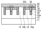
図22(a)は、本発明の一例の半導体装置1の活性領域の拡散構造を示す縦断面図であり、図22(b)は、活性領域と、その活性領域を取り囲む耐圧領域の拡散構造を示す縦断面図である。
【0028】
図31(a)は、図22(a)のV−V線の横断面図と図22(b)のW−W線の横切断面図に相当する図面であり、逆に、図22(a)、(b)は、それぞれ図31(a)のH−H線、J−J線の縦切断面図に相当する図面である。
【0029】
図22(a)、(b)の符号11は、シリコン単結晶等の半導体材料から成る第1導電型の半導体基板を示している。
【0030】
半導体基板11上には、半導体基板11と同じか、又は異なる半導体材料がエピタキシャル成長法によって成長され、第1導電型の単結晶層12が形成されている。
【0031】
単結晶層12内部の表面近傍位置には、複数個のベース拡散領域15aが配置されている。各ベース拡散領域15aは、第2導電型であり、単結晶層12とpn接合を形成している。符号14は、ベース拡散領域15aの下方に位置する単結晶層12から成るドレイン領域である。
【0032】
単結晶層12にはエッチングによって細長い直角四角形形状のゲート溝16aと逆阻止溝16bと、四角リング状のガード溝16cが形成されている。
【0033】
それらの溝のうち、ゲート溝16aはベース拡散領域15aの中央に1本又は二本以上配置されている。ここでは1本であるが、二本以上配置される場合は、互いに平行に配置される。逆阻止溝16bは、ゲート溝16aの両側に、ゲート溝16aに対して平行に配置されている。
【0034】
ガード溝16cはベース拡散領域15aの周囲に、ベース拡散領域15aを取り囲んで配置されている。
【0035】
各溝16a〜16cは、同一工程で形成されており、同じ深さ及び同じ幅にされている。また、各溝16a〜16cの深さはベース拡散領域15aよりも深く、且つ、半導体基板11には達しない程度の深さである。
【0036】
各溝16a〜16cのうち、逆阻止溝16bとガード溝16cの内部には、エピタキシャル成長によって形成された第2導電型の半導体材料が底面から上端部まで配置されており、その半導体材料によって、逆阻止領域33bとガード領域33cとがそれぞれ形成されている。
【0037】
他方、ゲート溝16aの内部では、下部にだけその半導体材料が配置されており、その半導体材料によって、埋込領域33aが構成されている。
【0038】
ここでは半導体材料はシリコン単結晶であるが、他の半導体の単結晶であってもよく、ポリシリコンのような多結晶であってもよい。
【0039】
符号13は、逆阻止領域33bで挟まれた単結晶層12の領域から成る整流領域である。
【0040】
ゲート溝16a内部の上部の半導体材料が存しない部分は、ゲート溝16aの底面及び側面にはゲート絶縁膜36が配置されている。ゲート絶縁膜36は、単結晶層12を熱酸化処理して形成する酸化物や、他の方法によって形成する窒化物膜等を用いることができる。
【0041】
ゲート溝16a内部のゲート絶縁膜36で囲まれた領域には、ゲート電極プラグ38が配置されている。
【0042】
ベース拡散領域15aの内部の表面近傍位置であって、ゲート絶縁膜36と接触する位置には、第1導電型のソース拡散領域19が配置されている。
【0043】
ベース拡散領域15aとソース拡散領域19の表面は露出され、その表面にソース電極膜44が配置されている。
【0044】
半導体基板11の裏面には、ドレイン電極膜43が配置されており、第1導電型がn型であるnチャネルMOSFETの場合、ソース電極膜44を接地させ、ドレイン電極膜43に正電圧を印加した状態で、ゲート電極プラグ38にしきい値電圧以上の正電圧を印加すると、ベース拡散領域15aのゲート絶縁膜36と接した部分が第1導電型に反転する。その反転によって第1導電型の反転層が形成され、反転層で、ソース拡散領域19とドレイン領域14とが接続され、反転層を通ってドレイン領域14からソース拡散領域19に電流が流れる。
【0045】
このとき、ベース拡散領域15aとドレイン領域14との間のpn接合は逆バイアスされており、pn接合には電流は流れない。
【0046】
整流領域13は、二本の逆阻止領域33bによって挟まれており、且つ、整流領域13の表面は露出され、ショットキー電極膜45と接触している。ここでは、ショットキー電極膜45はソース電極膜44と一緒に形成され、ソース電極膜44に接続されている。
【0047】
ショットキー電極膜45は、整流領域13とショットキー接合を形成する材料が選択されており、そのショットキー接合の極性は、ベース拡散領域15aと単結晶層12との間のpn接合が逆バイアスされる場合には、ショットキー接合も逆バイアスされ、pn接合が順バイアスされる場合には、ショットキー接合も順バイアスされるようになっている。
【0048】
逆阻止領域33bはソース電極膜44と接触し、その結果、逆阻止領域33bには、ベース拡散領域15aやソース拡散領域19に印加される電圧が印加される。
【0049】
逆阻止領域33bは第2導電型であり、整流領域13を含む単結晶層12とpn接合を形成している。ベース拡散領域15aと単結晶層12とが逆バイアスされるときには、逆阻止領域33bと整流領域13との間のpn接合も逆バイアスされる。従って、ショットキー電極膜45と整流領域13の間に形成されるショットキー接合が逆バイアスされるときには逆阻止領域33bと単結晶層12との間に形成されるpn接合も逆バイアスされる。
【0050】
逆バイアスにより、ショットキー接合から整流領域13内の深さ方向に向けて空乏層が広がる場合には、逆阻止領域33bから整流領域13内に向けて横方向に空乏層が広がる。
【0051】
整流領域13を挟んで隣接する逆阻止領域33b間の距離は、逆阻止領域33bの深さよりも小さくされており、ショットキー接合から広がった空乏層が、逆阻止領域33bの底部に達するよりも小さい電圧で、逆阻止領域33bから広がった空乏層同士が互いに接触する。その結果、整流領域13の内部はpn接合から広がった空乏層で満たされる。
【0052】
逆阻止領域33bの長さ方向に沿ったショットキー電極膜45の長さは、細長の逆阻止領域33bの長さよりも小さくされている。図31(b)は、その様子を示す平面図であり、逆阻止領域33bの長さY1の方が、ショットキー電極膜45の長さY2よりも長くなっている。
【0053】
従って、逆阻止領域33bの両端部分は、ショットキー電極膜45よりもはみ出しており、逆阻止領域33bの端部と、それに相対する逆阻止領域33bの端部との間の位置では、ショットキー電極膜45が配置されておらず、ショットキー接合は形成されていない。
【0054】
従って、対向する逆阻止領域33bから広がった空乏層が互いに接触したときには、ショットキー接合は、pn接合から広がった空乏層で覆われる。この状態では、等価回路上、逆バイアスされたショットキー接合と逆バイアスされたpn接合とは直列に接続された状態になる。
【0055】
一般に、ショットキー接合の逆方向の耐電圧は、pn接合の逆方向耐電圧に比べて小さいが、単結晶層12とショットキー電極膜45の間の逆方向耐電圧は、pn接合の耐電圧の大きさ以上になる。
【0056】
埋込領域33aは、ソース拡散領域19やドレイン領域14とは電気的に接続されておらず、浮遊電位に置かれている。逆バイアス状態のときベース拡散領域15aや逆阻止領域33bから単結晶層12の深さ方向に広がった空乏層が埋込領域33aに達すると、埋込領域33aの電位が安定し、埋込領域33aからも単結晶層12内に向けて空乏層が広がるようになる。
【0057】
活性領域内で、各溝16a〜16cの底部とベース拡散領域15aの底部間の部分では、その部分の第1導電型の領域(整流領域13を含む単結晶層12)が全部空乏化したときに、同じ部分の第2導電型の領域(埋込領域33aと逆阻止領域33bの底部)も全部空乏化するように、第1、第2の導電型の不純物総量が設定されている。各溝16a〜16c間に広がった空乏層は、更に各溝16a〜16cの底部から半導体基板11に向けて均等に広がる。
【0058】
ガード領域33cは、ソース拡散領域19やドレイン領域14とは電気的に接続されておらず、浮遊電位におかれている。ベース拡散領域15aや逆阻止領域33bから単結晶層12の横方向に向けて広がった空乏層が、ガード領域33cに達すると、ガード領域33cの電位が安定し、ガード領域33cからも更に横方向外側に向けて空乏層が広がる。
【0059】
結局、埋込領域33a及び逆阻止領域33bやガード領域33cが設けられているため、空乏層が大きく広がり、耐圧が高くなっている。
【0060】
上記のように、ベース拡散領域15aと単結晶層12との間のpn接合は、通常では逆バイアス状態に置かれているが、ドレイン電極膜43とソース電極膜44の電位が逆転し、ベース拡散領域15aと単結晶層12との間のpn接合が順バイアスされる場合は、ショットキー接合も順バイアスされる。
【0061】
pn接合とショットキー接合は並列接続されており、pn接合の順方向導通電圧よりもショットキー接合の順方向導通電圧の方が低いため、ショットキー接合に電流が流れ、pn接合は、導通したショットキー接合の順方向導通電圧によってクランプされ、電流は流れない。
【0062】
その状態からソース電極膜44とドレイン電極膜43の電圧の極性が反転し、ショットキー接合が順バイアス状態から逆バイアス状態になると、ショットキー接合の逆方向回復時間の経過後、電流は停止する。
【0063】
ショットキー接合の逆方向回復時間はpn接合の逆方向回復時間に比べて非常に短時間なので、電流が停止するまでの時間は短い。
【0064】
なお、pn接合には順方向電流が流れていないため、pn接合の逆方向回復時間は、電流が停止する時間に影響を与えない。
【0065】
次に、本発明の半導体装置の製造工程を説明する。特に断らない限り、絶縁膜や金属膜のパターニングはフォトレジスト工程とエッチング工程によって行うが、その説明は省略する。また、下記の各工程によって裏面に薄膜が形成される場合があるが、特に断らない限り、その説明は省略する。
【0066】
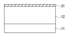
図1は、第1導電型の半導体基板11上に、第1導電型の単結晶層12がエピタキシャル成長によって形成され、更に、単結晶層12表面に、絶縁膜31が形成された状態の断面図を示している。ここでは、半導体基板11と単結晶層12はn型のシリコン単結晶であるが、他の半導体の単結晶であってもよい。また、この絶縁膜31及び後述する絶縁膜は、この例ではシリコン酸化膜であるが、シリコン窒化膜等の他の絶縁膜であってもよい。
【0067】
次に、絶縁膜31をパターニングする。図24はその状態の平面図であり、そのパターニングにより、絶縁膜31には、四角リング状であって、同心状に複数本配置されたリング状開口61と、最内周のリング状開口61で囲まれた複数の長方形のベース開口51が形成される。
【0068】
この図24及び後述する各平面図中の符号10は、一枚の半導体基板11上に形成される複数個の半導体装置1の境界を示している。一の半導体装置1の境界10と、同じ半導体基板11上の他の半導体装置1の境界10間は、互いに一定距離だけ離間しており、境界10と境界10との間の位置が切断されることで、複数の半導体装置1同士が分離されるようになっている。最外周のリング状開口61の外周は、境界10から一定距離だけ離れている。
【0069】
各ベース開口51は互いに平行に配置されている。また、各ベース開口51の四辺のうちの一辺は、リング状開口61の二辺に対して平行になっている。図2は、図24のA−A線切断面図である。
【0070】
ベース開口51とリング状開口61の底面には、単結晶層12が露出されており、絶縁膜31の上方から、ホウ素等の第2導電型の不純物を打ち込むと、ベース開口51の底面下に位置する単結晶層12の内部表面近傍部分に第2導電型の高濃度不純物領域が形成される。
【0071】
図3の符号21は、ベース開口51底面下に形成された高濃度不純物領域を示している。
【0072】
次に、熱処理を行い、高濃度不純物領域21を拡散させると、ベース開口51とリング状開口61の下方位置に、ベース開口51の形状とリング状開口61の形状に近似した第2導電型のベース拡散領域と補助拡散領域とがそれぞれ形成される。
【0073】
図25の符号15aはベース拡散領域を示しており、符号15cは、補助拡散領域を示している。図4は、図25のB−B線縦断面図に相当し、逆に、図25は、図4のQ−Q線横断面図に相当する。
【0074】
図4の符号32は、第2導電型の高濃度不純物領域21を拡散させた後に観察される酸化物膜を示しており、ベース拡散領域15aや補助拡散領域15cを含む単結晶層12の表面は、酸化物膜32によって覆われている。
【0075】
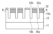
その状態から酸化物膜32をパターニングし、図26に示すように、ベース拡散領域15a上に位置し、平面形状が細長で長方形形状のゲート溝用窓開部52aと、逆阻止溝用窓開部52bとを形成し、補助拡散領域15cの幅方向中央に位置し、平面形状が四角リング状であって、ゲート溝用窓開部52a及び逆阻止溝用窓開部52bを取り囲む位置に、ガード溝用窓開部52cを形成する。
【0076】
ゲート溝用及び逆阻止溝用窓開部52a、52bは各ベース拡散領域15aの長辺に対して平行であり、ゲート溝用窓開部52aは、各ベース拡散領域15aの幅方向略中央位置に1乃至2本以上ずつ(本例では1本)配置され、逆阻止溝用窓開部52bは、各ベース拡散領域15aの相対する長辺上の位置、又は長辺近傍であってベース拡散領域15a内の位置に配置されている。
【0077】
従って、ゲート溝用窓開部52aと逆阻止溝用窓開部52bは互いに平行であり、且つ、1乃至2本以上のゲート溝用窓開部52aは、2本の逆阻止溝用窓開部52bの間に位置している。
【0078】
また、ガード溝用窓開部52cは直角四角形であり、ゲート溝用窓開部52aと逆阻止溝用窓開部52bは、ガード溝用窓開部52cの平行な二辺に対して平行になっている。
【0079】
図5は、図26のC−C線切断面図である。各溝用窓開部52a〜52cの底面には、ベース拡散領域15aの表面、又はベース拡散領域15aの表面と単結晶層12の表面とが露出されており、酸化物膜32をマスクとして単結晶層12のエッチングを行うと、図6、図27に示すように、ゲート溝用、逆阻止溝用、及びガード溝用窓開部52a〜52cの底面下に、それぞれゲート溝16a、逆阻止溝16b、及びガード溝16cがそれぞれ形成される。
【0080】
図6は、図27のD−D線切断面図に相当する図面であり、図27は、図6のR−R線切断面図に相当する図面である。
【0081】
各溝16a〜16cの断面形状は長方形であり、深さはベース拡散領域15aや補助拡散領域15cよりも深いため、各溝16a〜16cの底面は、ベース拡散領域15aの底面や補助拡散領域15cの底面と、半導体基板11の間に位置している。
【0082】
ガード溝16cの幅は、補助拡散領域15cの幅よりも狭く、ガード溝16cは、補助拡散領域15cの幅方向中央に位置しているため、各補助拡散領域15cは、中央部分が掘削され、外周部分と内周部分に二分される。
【0083】
なお、各溝16a〜16cは同一工程で形成されるため、同一深さになっている。また各溝16a〜16cの幅と、各溝16a〜16c間の間隔は等しくされている。
【0084】
次に、エピタキシャル成長法によって、各溝16a〜16cの内部側面及び底面に露出する単結晶層12(ベース拡散領域15aや補助拡散領域15cを含む。以下同じ。)の表面に第2導電型の半導体単結晶を成長させると、各溝16a〜16cの内部は、その半導体単結晶によって充填される。ここでは、半導体単結晶としてシリコン単結晶が用いられている。
【0085】
図7はその状態を示す図であり、符号34は、その各溝16a〜16c内に充填された充填物を示している。
【0086】
本発明の半導体装置では、各溝16a〜16cの開口の平面形状が直角四角形になっており、底面と側面から均一に半導体単結晶が成長し、内部が隙間なく充填される。
【0087】
各溝16a〜16c内の充填物34は、各溝16a〜16cの底面と側面に露出する単結晶層12に密着している。
【0088】
ここでは充填物34は、酸化物膜32の表面よりも高い位置まで盛り上がっており、エッチングにより、図8に示すように、単結晶層12よりも上の部分を除去し、次いで、図9に示すように、酸化物膜32を除去すると、各溝16a〜16cの間に位置する単結晶層12の表面が露出する。図9のS−S線切断面図を図28に示す。図9は、この図28のE−E線切断面図に相当する。
【0089】
図9及び図28の符号33a〜33cは、ゲート溝16a、逆阻止溝16b、ガード溝16c内に位置する充填物34から成る、埋込領域と、逆阻止領域と、ガード領域をそれぞれ示している。
【0090】
この状態では、埋込領域33aと逆阻止領域33bとは、ベース拡散領域15aと接触しており、ガード領域33cは、補助拡散領域15cに接触している。
【0091】
符号13は、ベース拡散領域15aや補助拡散領域15cが形成されていない単結晶層12の部分であり、一の逆阻止領域33bと他の逆阻止領域33bで挟まれた整流領域を示している。
【0092】
また、符号14は、ベース拡散領域15a底面の単結晶層12の部分であり、埋込領域33bとpn接合を形成し、空乏層が広がるドレイン領域を示している。
【0093】
次に、図10に示すように、酸化物膜35を単結晶層12表面に形成し、パターニングして埋込領域33aの表面だけを露出させ、酸化物膜35をマスクとして単結晶層12のエッチングを行い、埋込領域33aの上部を除去すると、図11と、そのT−T線切断面図の図29に示すように、ゲート溝16aの底部に埋込領域33aが残り、その上部に溝残部53が形成される。逆阻止領域33bやガード領域33cはエッチングされず、変化はない。
【0094】
埋込領域33aの上部はベース拡散領域15aの底面よりも低い位置までエッチングされており、埋込領域33aはベース拡散領域15aとは接触していない。従って、溝残部53の側面の上部には、上部にベース拡散領域15aが露出し、その下部にはドレイン領域14が露出している。溝残部53の底面には、埋込領域33aの上部が露出している。
【0095】
次に、図12に示すように、熱酸化により、溝残部53の側面と底面を含む単結晶層12の表面にゲート絶縁膜36を形成する。ゲート絶縁膜36は、溝残部53が閉塞されない膜厚にする。この状態では、溝残部53は、開口部分を除き、ゲート絶縁膜36によって囲まれている。
【0096】
次に、図13に示すように、ゲート絶縁膜36上に導電性を有するポリシリコン37を堆積させ、溝残部53内をポリシリコン37で埋める。
【0097】
次に、エッチング工程により、溝残部53内のポリシリコン37を残しながら、ポリシリコン37のゲート絶縁膜36の表面上に露出する部分を、一部を除いてエッチング除去すると、図14に示すように、溝残部53内にゲート電極プラグ38が形成される。ポリシリコン37のゲート絶縁膜36上に残った部分は図示されていないが、各ゲート溝16a内のゲート電極プラグ38に接続されており、後述するゲート電極パッドと接続される接続部分である。
【0098】
図30は、図14のU−U線切断面図である。図30では、ゲート絶縁膜36は省略してある。図14は、図30のG−G線断面図に相当する。
【0099】
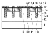
次に、単結晶層12上に位置し、露出されているゲート絶縁膜36をエッチングし、単結晶層12上のゲート絶縁膜36を除去すると、図15に示すように、ベース拡散領域15aや整流領域13の表面と、逆阻止領域33bが露出する。この状態では、ゲート溝16aの底面には、埋込領域33aが配置され、ゲート溝16aの埋込領域33aよりも上の位置には、ゲート絶縁膜36を介してゲート電極プラグ38が配置されている。ゲート電極プラグ38は、ゲート絶縁膜36を介してベース拡散領域15aとドレイン領域14に接している。
【0100】
次に、図16に示すように、熱酸化法によって、ベース拡散領域15aや整流領域13上に薄い酸化膜39を形成した後、その表面に、図17に示すように、パターニングしたレジスト膜40を配置する。
【0101】
このレジスト膜40は、各ゲート溝16aの両側に、ゲート溝16aの長手方向に沿った細長い開口54を有している。開口54の幅はベース拡散領域15aの幅よりも狭く、逆阻止溝16bには達していない。
【0102】
その状態で、レジスト膜40の上方から第1導電型の不純物を照射すると、不純物は薄い酸化膜39を透過し、図18に示すように、開口54底面の位置に第1導電型の不純物の高濃度領域18が形成される。
【0103】
次に、レジスト膜40を除去した後、熱処理し、高濃度領域18中の第1導電型の不純物を拡散させると、図19に示すように、ゲート溝16aの長手方向両側の位置に、ゲート絶縁膜36と接触してソース拡散領域19が形成される。ソース拡散領域19はベース拡散領域15aよりも浅くなっており、ゲート絶縁膜36は、上端部でソース拡散領域19と接触し、その下方位置でベース拡散領域15aとドレイン領域14に接触している。ゲート電極プラグ38は、ソース拡散領域19とベース拡散拡散領域15aとドレイン領域14とに、ゲート絶縁膜36を介して接している。
【0104】
図19の符号41は、ソース拡散領域19を形成する際に形成される酸化膜である。
【0105】
次に、その酸化膜41をパターニングし、図20に示すように、ゲート電極プラグ38の上部に酸化膜41を残し、ソース拡散領域19と、ベース拡散領域15aと、整流領域13と、逆阻止領域33bの表面の全部又は一部を露出させた後、スパッタ法や蒸着法等により、その表面に金属薄膜42を形成する。
【0106】
この金属薄膜42は、ソース拡散領域19と、ベース拡散領域15aと、整流領域13と、逆阻止領域33bの表面に接触しており、整流領域13とはショットキー接合を形成し、他の領域19、15a、33bとはオーミック接合を形成する金属であり、ソース拡散領域19と、ベース拡散領域15aと、逆阻止領域33bとは、この金属薄膜42によって短絡されている。また、金属薄膜42は、図示されていないゲート電極プラグ38の接続部分に接続されている。
【0107】
整流領域13と金属薄膜42とが形成するショットキー接合は、金属薄膜42と基板11との間に電圧が印加され、ベース拡散領域15aとドレイン領域14との間のpn接合が順バイアスされるときに順バイアスされ、逆バイアスされるときに逆バイアスされる極性になっている。
【0108】
従って、ベース拡散領域15aとドレイン領域14との間のpn接合と、金属薄膜42と整流領域13との間のショットキー接合は、並列接続されている。
【0109】
次に、金属薄膜42を二分割し、ゲート電極プラグ38の接続部分に接続された金属薄膜42の一部領域を、ベース拡散領域15aやソース拡散領域19に接続された領域から分離し、ゲート電極パッドとする。また、後者をソース電極膜とする。
【0110】
次に、図22(a)、(b)に示すように、半導体基板11の裏面に半導体基板11とオーミック接合を形成するドレイン電極膜43を形成すると、本発明の半導体装置1が得られる。
【0111】
同図(a)、(b)の符号44はゲート電極パッドから分離された金属薄膜42のうち、ソース拡散領域19やベース拡散領域15aと接続されたソース電極膜を示しており、符号45は、整流領域13と接触し、ショットキー接合を形成するショットキー電極膜を示している。なお、上述したように、この図22(a)のV−V線、及び同図(b)のW−W線の横断面図に相当する図面は、図31(a)に示されている。
【0112】
次に、上記ソース電極膜44やショットキー電極膜45上に保護膜を形成し、ソース電極膜44の一部領域をソース電極パッドとし、ソース電極パッドとゲート電極パッドを露出させた後、同一半導体基板11上に形成された複数の半導体装置1を分割し、各半導体装置1のドレイン電極膜43をリードフレームに接触させて、それぞれリードフレームに搭載した後、ソース電極パッドとゲート電極パッドをワイヤーボンディングによってリードに接続し、半導体装置1を樹脂封止した後、リードを切断して個別に分離すると、樹脂封止された半導体装置1が得られる。
【0113】
なお、図23(a)の半導体装置2のように、先ず、整流領域13とショットキー接合を形成し、他の領域19、15a、33bとはオーミック接合を形成するショットキー電極膜45を成膜した後、その表面に、低抵抗のソース電極膜44を形成してもよい。
【0114】
また、図23(b)の半導体装置3のように、最初に成膜したショットキー電極膜45をパターニングし、ソース拡散領域19やベース拡散領域15aを露出させた後、ソース電極膜44を形成してもよい。
【0115】
また、上記例では、図11において、埋込領域33aの上部をベース拡散領域15aの底面よりも低い位置までエッチングする際にゲート溝16aの長さ方向の全範囲の上部をエッチングしたが、ゲート溝16aは細長であるから、ゲート溝16aの長さ方向の一部をマスクし、その部分の埋込領域33aをエッチングせずに残すことが可能である。
【0116】
この場合、例えば、図示はしないが、ゲート溝16aの両端部分だけを酸化物膜32で覆っておき、露出部分をベース拡散領域15aよりも深い位置までエッチングすると、エッチングされなかった部分は、ゲート溝16aの下端部から上端部まで埋込領域33aが残る。
【0117】
その埋込領域33aはベース拡散領域15aに接触しているため、その部分が接続領域となり、上部がエッチング除去された埋込領域33aがベース拡散領域15aに接続される。上記実施例が、埋込領域33aが浮遊電位に置かれていたのに対し、この場合は、埋込領域33aはベース拡散領域15aと同じ電位になり、埋込領域33aからは、ベース拡散領域15aと一緒に空乏層が広がる。
【0118】
上記各実施例では、逆阻止溝16bは細長い直角四角形形状であり、整流領域13を挟んでいたが、四辺が直角四角形形状の四角リング状に形成し、整流領域13を取り囲むようにしてもよい。
【0119】
図32の符号4は、その四角リング形状の逆阻止溝16b'を有する半導体装置4を示しており、この逆阻止溝16b'の内部にも、第2導電型の半導体材料が充填され、整流領域13を取り囲む逆阻止領域33b'が形成されている。ショットキー電極膜45は、逆阻止領域33b'で囲まれた整流領域13と接触し、ショットキー接合を形成しているが、逆阻止領域33b'の外側に位置する単結晶層12の表面とは接触していない。
【0120】
なお、この半導体装置4のH'−H'線、J'−J'線の切断面図は、図31(a)のH−H線、J−J線の切断面図と同じ、図22(a)、(b)である。
【0121】
上記のように、本発明の半導体装置には、整流領域13が、互いに分離された逆阻止溝16bで挟まれる場合の他、リング状に成形された逆阻止溝16b'やコ字型形状に接続された逆阻止溝の二辺以上の辺で挟まれた場合も含まれる。
【0122】
【発明の効果】
ショットキーダイオードがあるため、逆方向の回復が速く、また、逆阻止領域により、ショットキーダイオードの耐圧が高くなっている。
【図面の簡単な説明】
【図1】本発明の一例の半導体装置の製造工程を説明するための活性領域の切断面図(1)
【図2】本発明の一例の半導体装置の製造工程を説明するための活性領域の切断面図(2)
【図3】本発明の一例の半導体装置の製造工程を説明するための活性領域の切断面図(3)
【図4】本発明の一例の半導体装置の製造工程を説明するための活性領域の切断面図(4)
【図5】本発明の一例の半導体装置の製造工程を説明するための活性領域の切断面図(5)
【図6】本発明の一例の半導体装置の製造工程を説明するための活性領域の切断面図(6)
【図7】本発明の一例の半導体装置の製造工程を説明するための活性領域の切断面図(7)
【図8】本発明の一例の半導体装置の製造工程を説明するための活性領域の切断面図(8)
【図9】本発明の一例の半導体装置の製造工程を説明するための活性領域の切断面図(9)
【図10】本発明の一例の半導体装置の製造工程を説明するための活性領域の切断面図(10)
【図11】本発明の一例の半導体装置の製造工程を説明するための活性領域の切断面図(11)
【図12】本発明の一例の半導体装置の製造工程を説明するための活性領域の切断面図(12)
【図13】本発明の一例の半導体装置の製造工程を説明するための活性領域の切断面図(13)
【図14】本発明の一例の半導体装置の製造工程を説明するための活性領域の切断面図(14)
【図15】本発明の一例の半導体装置の製造工程を説明するための活性領域の切断面図(15)
【図16】本発明の一例の半導体装置の製造工程を説明するための活性領域の切断面図(16)
【図17】本発明の一例の半導体装置の製造工程を説明するための活性領域の切断面図(17)
【図18】本発明の一例の半導体装置の製造工程を説明するための活性領域の切断面図(18)
【図19】本発明の一例の半導体装置の製造工程を説明するための活性領域の切断面図(19)
【図20】本発明の一例の半導体装置の製造工程を説明するための活性領域の切断面図(20)
【図21】本発明の一例の半導体装置の製造工程を説明するための活性領域の切断面図(21)
【図22】(a):本発明の一例の半導体装置の製造工程を説明するための活性領域の切断面図(21) (b):それに対応する活性領域周囲の断面図
【図23】(a)、(b):本発明の半導体装置の他の例を説明するための活性領域の断面図
【図24】図2の状態の平面図
【図25】図4の状態に対応する横方向の断面図
【図26】図5の状態の平面図
【図27】図6の状態に対応する横方向の断面図
【図28】図9の状態に対応する横方向の断面図
【図29】図11の状態に対応する横方向の断面図
【図30】図14の状態に対応する横方向の断面図
【図31】(a):図22(a)、(b)に対応する横方向の断面図 (b):逆阻止領域とショットキー電極の長さの大小を説明するための図
【図32】本発明の第四例の半導体装置の平面図
【図33】従来技術のMOSFETの拡散構造を説明するための平面図
【図34】(a):そのI−I線切断面図 (b):II−II線切断面図
【符号の説明】
1〜4……半導体装置
12……単結晶層
13……整流領域
14……ドレイン領域
15a……ベース拡散領域
16a……ゲート溝
16b、16b'……逆阻止溝
16c……ガード溝
19……ソース拡散領域
33a……埋込領域
33b、33b'……逆阻止領域
33c……ガード領域
36……ゲート絶縁膜
38……ゲート電極プラグ
43……ドレイン電極膜
44……ソース電極膜
45……ショットキー電極膜[0001]
BACKGROUND OF THE INVENTION
The present invention relates to a semiconductor device, and more particularly to a semiconductor device in which an active region is surrounded by a semiconductor single crystal disposed in a trench.
[0002]
[Prior art]
FIG. 33 is a plan view for explaining the diffusion structure of the
[0003]
The
[0004]
A
[0005]
A p-type
[0006]
A plurality of elongated
[0007]
Between two adjacent
[0008]
A plurality of square ring-
[0009]
A
[0010]
On the other hand, the
[0011]
An
[0012]
A
[0013]
The
[0014]
Conversely, when the
[0015]
From this state, even if the pn junction between the
[0016]
In order to prevent this, a Schottky diode is externally connected in parallel with the pn junction between the
[0017]
[Problems to be solved by the invention]
The present invention was created to solve the above-described disadvantages of the semiconductor device, and an object thereof is to provide a transistor having a short reverse recovery time.
[0018]
[Means for Solving the Problems]
In order to solve the above-mentioned problem, the invention described in
A second aspect of the present invention is the semiconductor device according to the first aspect, comprising a plurality of the transistors and the Schottky diodes.
The invention according to
The invention according to
The invention according to claim 55. The semiconductor device according to
The invention described in claim 6A connection region of a second conductivity type in contact with the buried region and the base diffusion region is disposed on the bottom surface in the gate trench, and the buried region and the base diffusion region are electrically connected by the connection region. 5. The semiconductor device according to
According to a seventh aspect of the present invention, a plurality of concentric ring-shaped guard grooves are formed in the single crystal layer, and each of the guard grooves is made of the semiconductor material of the second conductivity type. A guard region that forms a pn junction with the single crystal layer is disposed, and the gate groove and the reverse blocking groove are surrounded by the innermost guard groove.6The semiconductor device according to any one of the above.
[0019]
The present invention is configured as described above, and the Schottky junction is sandwiched between the reverse blocking grooves parallel to each other, and from the reverse blocking region disposed inside the reverse blocking groove toward the lower side of the Schottky junction. The depletion layer extends.
[0020]
The length in the direction along the reverse blocking groove of the Schottky junction is shorter than that of the reverse blocking groove, and the reverse blocking region inside the reverse blocking groove protrudes on both sides of the Schottky junction. . A pn junction is formed between the reverse blocking region and the rectifying region, and when the depletion layer spreads from the reverse blocking groove positioned opposite to each other and the depletion layers contact each other under the Schottky junction, Covered with a depletion layer, equivalently, a pn junction in a reverse bias state and a Schottky junction in a reverse bias state are connected in series.
[0021]
Since the withstand voltage of the series connection circuit is determined by the withstand voltage of the pn junction between the reverse blocking region and the rectifying region, it is larger than the withstand voltage of the Schottky junction.
[0022]
The reverse blocking groove is formed together with the gate groove and the guard groove, and the depth of each groove is equal. A buried region that forms a pn junction with the drain region is disposed at the bottom of the gate trench.
[0023]
When there are other buried regions adjacent to the buried region, the distances a between them are equal to each other.
[0024]
When there is a reverse blocking region adjacent to the buried region, the distance b between the buried region and the reverse blocking region is equal to each other, and the distance a and the distance b are also equal to each other.
[0025]
Therefore, when a reverse voltage is applied so that the depletion layers in the opposite blocking regions located opposite to each other are in contact with each other, the depletion layer that spreads from the buried region is depleted from the other buried region or the reverse layer. Since it contacts the depletion layer extending from the blocking region, the breakdown voltage of the transistor is also increased.
[0026]
DETAILED DESCRIPTION OF THE INVENTION
Embodiments of the present invention will be described below with reference to the drawings.
In this embodiment and each of the embodiments described later, if the first conductivity type is n-type, the second conductivity type is p-type, and if the first conductivity type is p-type, the second conductivity type is n-type. . The present invention includes both cases.
[0027]
FIG. 22A is a longitudinal sectional view showing a diffusion structure of the active region of the
[0028]
31A is a drawing corresponding to a cross-sectional view taken along the line VV in FIG. 22A and a cross-sectional view taken along the line WW in FIG. 22B. Conversely, FIG. (a), (b) is drawing equivalent to the longitudinal cross-sectional view of the HH line | wire and JJ line | wire of FIG.
[0029]
[0030]
On the
[0031]
A plurality of
[0032]
Single crystal layer
[0033]
Among these grooves, one or
[0034]
The
[0035]
The
[0036]
Among the
[0037]
On the other hand, in the
[0038]
Here, the semiconductor material is a single crystal of silicon, but it may be a single crystal of another semiconductor or a polycrystal such as polysilicon.
[0039]
[0040]
A
[0041]
A
[0042]
A
[0043]
The surfaces of the
[0044]
A
[0045]
At this time, the pn junction between the
[0046]
The rectifying
[0047]
For the
[0048]
The
[0049]
The
[0050]
When the depletion layer spreads from the Schottky junction in the depth direction in the
[0051]
The distance between the
[0052]
The length of the
[0053]
Therefore, both end portions of the
[0054]
Therefore, when the depletion layers extending from the opposite
[0055]
In general, the reverse withstand voltage of the Schottky junction is smaller than the reverse withstand voltage of the pn junction, but the reverse withstand voltage between the
[0056]
The buried
[0057]
In the active region, in the portion between the bottom of each of the
[0058]
The
[0059]
Eventually, since the buried
[0060]
As described above, the pn junction between the
[0061]
The pn junction and the Schottky junction are connected in parallel. Since the forward conduction voltage of the Schottky junction is lower than the forward conduction voltage of the pn junction, a current flows through the Schottky junction, and the pn junction becomes conductive. Clamped by the forward conduction voltage of the Schottky junction, no current flows.
[0062]
When the polarity of the voltage of the
[0063]
Since the reverse recovery time of the Schottky junction is much shorter than the reverse recovery time of the pn junction, the time until the current stops is short.
[0064]
Since no forward current flows through the pn junction, the reverse recovery time of the pn junction does not affect the time when the current stops.
[0065]
Next, the manufacturing process of the semiconductor device of the present invention will be described. Unless otherwise specified, the patterning of the insulating film and the metal film is performed by a photoresist process and an etching process, but the description thereof is omitted. In addition, a thin film may be formed on the back surface by the following steps, but the description is omitted unless otherwise specified.
[0066]
FIG. 1 is a cross-sectional view of a state in which a first conductivity type
[0067]
Next, the insulating
[0068]
[0069]
The
[0070]
The
[0071]
[0072]
Next, heat treatment is performed to form a high concentration impurity region.21Is diffused, a base diffusion region of the second conductivity type and an auxiliary diffusion region that approximate the shape of the
[0073]
[0074]
[0075]
From this state, the
[0076]
The gate groove and reverse blocking
[0077]
Therefore, the gate
[0078]
The guard
[0079]
FIG. 5 is a sectional view taken along the line CC of FIG. The surface of
[0080]
6 is a drawing corresponding to the sectional view taken along the line DD of FIG. 27, and FIG. 27 is a drawing corresponding to the sectional view taken along the line RR of FIG.
[0081]
The cross-sectional shape of each of the
[0082]
The width of the
[0083]
In addition, since each groove |
[0084]
Next, the single crystal layer 12 (
[0085]
FIG. 7 is a diagram showing the state, and
[0086]
In the semiconductor device of the present invention, the planar shape of the opening of each of the
[0087]
The
[0088]
Here, the filling 34 isOxide film 32As shown in FIG. 8, the portion above the
[0089]
[0090]
In this state, the buried
[0091]
[0092]
[0093]
Next, as shown in FIG.Single crystalFormed on the surface of the
[0094]
The upper portion of the buried
[0095]
Next, as shown in FIG. 12, a
[0096]
Next, as shown in FIG. 13,
[0097]
Next, when the part exposed on the surface of the
[0098]
30 is a cross-sectional view taken along the line U-U in FIG. In FIG. 30, the
[0099]
Next, when the exposed
[0100]
Next, as shown in FIG. 16, the base is formed by thermal oxidation.diffusionThin on
[0101]
The resist
[0102]
In this state, when the first conductivity type impurity is irradiated from above the resist
[0103]
Next, after removing the resist
[0104]
[0105]
Next, the
[0106]
The metal
[0107]
In the Schottky junction formed by the rectifying
[0108]
Therefore, the pn junction between the
[0109]
Next, the metal
[0110]
Next, as shown in FIGS. 22A and 22B, when the
[0111]
In FIGS. 4A and 4B,
[0112]
Next, a protective film is formed on the
[0113]
In addition,Like the
[0114]
Further, as in the
[0115]
In the above example, in FIG. 11, when the upper portion of the buried
[0116]
In this case, for example, although not shown, only the both end portions of the
[0117]
The buried
[0118]
In each of the embodiments described above, the
[0119]
Reference numeral 4 in FIG. 32 shows the semiconductor device 4 having the square ring-shaped
[0120]
The sectional view taken along lines H′-H ′ and J′-J ′ of the semiconductor device 4 is the same as the sectional view taken along lines HH and JJ in FIG. (a), (b).
[0121]
As described above, the semiconductor device of the present invention includes a rectifying region.13Is sandwiched between two or more sides of a
[0122]
【The invention's effect】
Since there is a Schottky diode, recovery in the reverse direction is fast, and the breakdown voltage of the Schottky diode is high due to the reverse blocking region.
[Brief description of the drawings]
FIG. 1 is a sectional view (1) of an active region for explaining a manufacturing process of a semiconductor device according to an example of the present invention;
FIG. 2 is a sectional view (2) of an active region for explaining a manufacturing process of a semiconductor device according to an example of the present invention;
FIG. 3 is a cross-sectional view of an active region for explaining a manufacturing process of a semiconductor device according to an example of the present invention (3).
FIG. 4 is a sectional view (4) of an active region for explaining a manufacturing process of a semiconductor device according to an example of the present invention;
FIG. 5 is a sectional view of an active region for explaining a manufacturing process of a semiconductor device according to an example of the present invention (5);
FIG. 6 is a sectional view of an active region for explaining a manufacturing process of a semiconductor device according to an example of the present invention (6).
FIG. 7 is a sectional view of an active region for explaining a manufacturing process of a semiconductor device according to an example of the present invention (7).
FIG. 8 is a sectional view of an active region for explaining a manufacturing process of a semiconductor device according to an example of the present invention (8);
FIG. 9 is a sectional view of an active region for explaining a manufacturing process of an example semiconductor device of the present invention (9).
FIG. 10 is a sectional view (10) of an active region for explaining a manufacturing process of a semiconductor device according to an example of the present invention;
FIG. 11 is a sectional view (11) of an active region for explaining a manufacturing process of a semiconductor device according to an example of the present invention;
FIG. 12 is a sectional view (12) of an active region for explaining a manufacturing process of a semiconductor device according to an example of the present invention;
FIG. 13 is a sectional view (13) of an active region for explaining a manufacturing process of a semiconductor device according to an example of the present invention;
FIG. 14 is a cross-sectional view (14) of an active region for explaining a manufacturing process of a semiconductor device according to an example of the present invention;
FIG. 15 is a sectional view of an active region for explaining a manufacturing process of an example of a semiconductor device of the present invention (15);
FIG. 16 is a sectional view (16) of an active region for explaining a manufacturing process of a semiconductor device according to an example of the present invention;
FIG. 17 is a sectional view (17) of an active region for explaining a manufacturing process of a semiconductor device according to an example of the present invention;
FIG. 18 is a sectional view (18) of an active region for explaining a manufacturing process of a semiconductor device according to an example of the present invention;
FIG. 19 is a sectional view (19) of an active region for explaining a manufacturing process of a semiconductor device according to an example of the present invention;
FIG. 20 is a cross-sectional view of an active region for explaining a manufacturing process of an example semiconductor device of the present invention (20).
FIG. 21 is a sectional view (21) of an active region for explaining a manufacturing process of a semiconductor device according to an example of the present invention;
22A is a cross-sectional view of an active region for explaining a manufacturing process of a semiconductor device according to an example of the present invention; FIG.
23A and 23B are cross-sectional views of active regions for explaining another example of the semiconductor device of the present invention.
24 is a plan view of the state of FIG.
25 is a lateral sectional view corresponding to the state of FIG.
26 is a plan view of the state of FIG.
27 is a lateral cross-sectional view corresponding to the state of FIG.
28 is a lateral sectional view corresponding to the state of FIG.
29 is a lateral cross-sectional view corresponding to the state of FIG.
30 is a lateral cross-sectional view corresponding to the state of FIG.
31A is a lateral cross-sectional view corresponding to FIGS. 22A and 22B. FIG. 31B is a diagram for explaining the size of the length of the reverse blocking region and the Schottky electrode.
FIG. 32 is a plan view of a semiconductor device according to a fourth example of the present invention.
FIG. 33 is a plan view for explaining the diffusion structure of a MOSFET according to the prior art;
FIG. 34 (a): Its II line cut surface view (b): II-II line cut surface view
[Explanation of symbols]
1-4 ... Semiconductor device
12 ... Single crystal layer
13 …… Rectification area
14 …… Drain region
15a …… Base diffusion region
16a …… Gate groove
16b, 16b '... Reverse blocking groove
16c …… Guard groove
19 …… Source diffusion region
33a …… Embedded area
33b, 33b '... reverse blocking region
33c …… Guard area
36 …… Gate insulation film
38 …… Gate electrode plug
43 …… Drain electrode film
44 …… Source electrode film
45 …… Schottky electrode film
Claims (7)
前記単結晶層の内部の表面側に形成された第2導電型のベース拡散領域と、
前記単結晶層のベース拡散領域の底面よりも深い部分であるドレイン領域と、
前記ベース拡散領域の内部の表面側に形成され、前記ベース拡散領域によって前記ドレイン領域とは絶縁された第1導電型のソース拡散領域と、
前記単結晶層に、前記ベース拡散領域の深さよりも深く形成された溝であって、前記ソース拡散領域と、前記ソース拡散領域と前記ドレイン領域との間に位置するベース拡散領域と、前記ドレイン領域とに接触する位置に配置されたゲート溝と、
前記ゲート溝内部の側面に位置し、上部が前記ソース拡散領域と接触し、下部が前記ドレイン領域と接触し、中間部が前記ベース拡散領域と接触して配置されたゲート絶縁膜と、
前記ゲート溝の内部に位置し、前記ソース拡散領域から前記ドレイン領域の範囲に亘って、前記ゲート絶縁膜と接触して配置されたゲート電極プラグとを有し、
前記ゲート電極プラグに電圧を印加し、前記ベース拡散領域の前記ゲート絶縁膜と接触する部分に反転層を形成すると、前記ソース拡散領域と前記ドレイン領域とが前記反転層で接続されるように構成されたトランジスタと、
前記単結晶層に形成され前記ベース拡散領域と接触した逆阻止溝と、
前記逆阻止溝と前記逆阻止溝とで挟まれた部分の前記単結晶層である整流領域の表面に形成され、前記整流領域とショットキー接合を形成するショットキー電極膜とを有するショットキーダイオードと、
前記各逆阻止溝の内部には、第2導電型の半導体材料から成り、前記整流領域とpn接合を形成し、前記ベース拡散領域に印加される電圧が印加される逆阻止領域が配置されて形成されたpnダイオードと、
を有し、
前記ゲート溝内部の底面と前記ゲート電極プラグとの間の位置には、第2導電型の半導体材料から成る埋込領域が前記ゲート電極プラグとは絶縁された状態で配置され、
前記ゲート溝と前記逆阻止溝の深さは同一にされ、前記埋込領域と前記逆阻止領域の底部は前記ゲート溝と前記逆阻止溝の底面にそれぞれ接触された半導体装置。A semiconductor device having a single crystal layer of a first conductivity type,
A base diffusion region of a second conductivity type formed on the inner surface side of the single crystal layer;
A drain region that is deeper than the bottom surface of the base diffusion region of the single crystal layer;
A source diffusion region of a first conductivity type formed on the inner surface side of the base diffusion region and insulated from the drain region by the base diffusion region;
A groove formed in the single crystal layer deeper than a depth of the base diffusion region, the source diffusion region, a base diffusion region located between the source diffusion region and the drain region, and the drain a gate groove which is placed in contact in the region,
A gate insulating film disposed on a side surface inside the gate trench, wherein an upper portion is in contact with the source diffusion region, a lower portion is in contact with the drain region, and an intermediate portion is in contact with the base diffusion region;
A gate electrode plug located inside the gate trench and disposed in contact with the gate insulating film over a range from the source diffusion region to the drain region;
The source diffusion region and the drain region are connected by the inversion layer when a voltage is applied to the gate electrode plug and an inversion layer is formed in a portion of the base diffusion region that contacts the gate insulating film. A transistor,
A reverse blocking groove formed in the single crystal layer and in contact with the base diffusion region ;
Schottky diode having a Schottky electrode film forming the formed on the surface of the rectifying region is a single crystal layer, the rectifier area and a Schottky junction of the portion sandwiched between the reverse blocking groove and the reverse blocking groove When,
Wherein the interior of the reverse blocking groove made of a semiconductor material of a second conductivity type, said rectification region and pn junction is formed, a voltage applied to the base diffusion region is arranged reverse blocking area to be applied A formed pn diode;
I have a,
A buried region made of a semiconductor material of a second conductivity type is disposed at a position between the bottom surface inside the gate groove and the gate electrode plug in a state of being insulated from the gate electrode plug,
The depths of the gate groove and the reverse blocking groove are the same, and the bottom of the buried region and the reverse blocking region are in contact with the bottom surface of the gate groove and the reverse blocking groove, respectively .
前記ソース電極膜と前記ショットキー電極膜とは互いに接続された請求項1又は請求項2のいずれか1項記載の半導体装置。A source electrode film connected to the source diffusion region and the base diffusion region;
The source electrode film and the semiconductor device according to any one of the Schottky claims the electrode film are connected to each other 1 or claim 2.
前記ゲート溝と前記逆阻止溝とは、最内周の前記ガード溝によって取り囲まれた請求項1乃至請求項6のいずれか1項記載の半導体装置。A plurality of concentric ring-shaped guard grooves are formed in the single crystal layer, and each guard groove is made of the semiconductor material of the second conductivity type, and has a pn junction with the single crystal layer A guard region is formed,
Wherein the gate trench and the reverse blocking groove, the semiconductor device according to any one of claims 1 to 6 surrounded by the innermost of the guard groove.
Priority Applications (1)
| Application Number | Priority Date | Filing Date | Title |
|---|---|---|---|
| JP2003005271A JP4406535B2 (en) | 2003-01-14 | 2003-01-14 | Transistor with Schottky diode |
Applications Claiming Priority (1)
| Application Number | Priority Date | Filing Date | Title |
|---|---|---|---|
| JP2003005271A JP4406535B2 (en) | 2003-01-14 | 2003-01-14 | Transistor with Schottky diode |
Publications (3)
| Publication Number | Publication Date |
|---|---|
| JP2004221218A JP2004221218A (en) | 2004-08-05 |
| JP2004221218A5 JP2004221218A5 (en) | 2005-10-27 |
| JP4406535B2 true JP4406535B2 (en) | 2010-01-27 |
Family
ID=32895962
Family Applications (1)
| Application Number | Title | Priority Date | Filing Date |
|---|---|---|---|
| JP2003005271A Expired - Fee Related JP4406535B2 (en) | 2003-01-14 | 2003-01-14 | Transistor with Schottky diode |
Country Status (1)
| Country | Link |
|---|---|
| JP (1) | JP4406535B2 (en) |
Cited By (1)
| Publication number | Priority date | Publication date | Assignee | Title |
|---|---|---|---|---|
| CN107293601A (en) * | 2016-04-12 | 2017-10-24 | 朱江 | A kind of Schottky semiconductor device and preparation method thereof |
Families Citing this family (5)
| Publication number | Priority date | Publication date | Assignee | Title |
|---|---|---|---|---|
| WO2008069145A1 (en) * | 2006-12-04 | 2008-06-12 | Sanken Electric Co., Ltd. | Insulating-gate fet and its manufacturing method |
| JP5526496B2 (en) * | 2008-06-02 | 2014-06-18 | サンケン電気株式会社 | Field effect semiconductor device and manufacturing method thereof |
| DE102009028240A1 (en) * | 2009-08-05 | 2011-02-10 | Robert Bosch Gmbh | Field effect transistor with integrated TJBS diode |
| JP2012248686A (en) * | 2011-05-27 | 2012-12-13 | Elpida Memory Inc | Semiconductor device and manufacturing method of the same |
| JP6036765B2 (en) * | 2014-08-22 | 2016-11-30 | トヨタ自動車株式会社 | Semiconductor device and manufacturing method of semiconductor device |
-
2003
- 2003-01-14 JP JP2003005271A patent/JP4406535B2/en not_active Expired - Fee Related
Cited By (2)
| Publication number | Priority date | Publication date | Assignee | Title |
|---|---|---|---|---|
| CN107293601A (en) * | 2016-04-12 | 2017-10-24 | 朱江 | A kind of Schottky semiconductor device and preparation method thereof |
| CN107293601B (en) * | 2016-04-12 | 2021-10-22 | 朱江 | Schottky semiconductor device and preparation method thereof |
Also Published As
| Publication number | Publication date |
|---|---|
| JP2004221218A (en) | 2004-08-05 |
Similar Documents
| Publication | Publication Date | Title |
|---|---|---|
| JP4892172B2 (en) | Semiconductor device and manufacturing method thereof | |
| US7135718B2 (en) | Diode device and transistor device | |
| KR100843532B1 (en) | Semiconductor device | |
| JP2018082158A (en) | Semiconductor device | |
| JP3971670B2 (en) | Semiconductor device | |
| JP4406535B2 (en) | Transistor with Schottky diode | |
| JP3914852B2 (en) | Diode element and transistor element | |
| JP4794546B2 (en) | Semiconductor device and manufacturing method thereof | |
| US6563169B1 (en) | Semiconductor device with high withstand voltage and a drain layer having a highly conductive region connectable to a diffused source layer by an inverted layer | |
| JP4095492B2 (en) | Semiconductor device | |
| US7282764B2 (en) | Semiconductor device | |
| JP4133565B2 (en) | Transistor, method of manufacturing the same, and diode | |
| JP3738127B2 (en) | High voltage semiconductor device | |
| JP4929559B2 (en) | Semiconductor element | |
| JP6555284B2 (en) | Semiconductor device | |
| JP2007109712A (en) | Transistor and diode | |
| JP4133548B2 (en) | Semiconductor device | |
| JP7329348B2 (en) | semiconductor equipment | |
| JP4294016B2 (en) | Manufacturing method of semiconductor device | |
| WO2023062951A1 (en) | Silicon carbide semiconductor device | |
| JP4125864B2 (en) | Field effect transistor | |
| JP2005285983A (en) | Semiconductor device and method for manufacturing semiconductor device | |
| JP4851075B2 (en) | Manufacturing method of semiconductor device | |
| JP2006066609A (en) | Semiconductor device | |
| JP2005093479A (en) | Semiconductor device and its fabricating process |
Legal Events
| Date | Code | Title | Description |
|---|---|---|---|
| A521 | Request for written amendment filed |
Free format text: JAPANESE INTERMEDIATE CODE: A523 Effective date: 20050706 Free format text: JAPANESE INTERMEDIATE CODE: A821 Effective date: 20050706 |
|
| A621 | Written request for application examination |
Free format text: JAPANESE INTERMEDIATE CODE: A621 Effective date: 20050706 |
|
| A977 | Report on retrieval |
Free format text: JAPANESE INTERMEDIATE CODE: A971007 Effective date: 20080215 |
|
| A131 | Notification of reasons for refusal |
Free format text: JAPANESE INTERMEDIATE CODE: A131 Effective date: 20090512 |
|
| A521 | Request for written amendment filed |
Free format text: JAPANESE INTERMEDIATE CODE: A523 Effective date: 20090710 Free format text: JAPANESE INTERMEDIATE CODE: A821 Effective date: 20090710 |
|
| TRDD | Decision of grant or rejection written | ||
| A01 | Written decision to grant a patent or to grant a registration (utility model) |
Free format text: JAPANESE INTERMEDIATE CODE: A01 Effective date: 20091028 |
|
| A01 | Written decision to grant a patent or to grant a registration (utility model) |
Free format text: JAPANESE INTERMEDIATE CODE: A01 |
|
| A61 | First payment of annual fees (during grant procedure) |
Free format text: JAPANESE INTERMEDIATE CODE: A61 Effective date: 20091109 |
|
| FPAY | Renewal fee payment (event date is renewal date of database) |
Free format text: PAYMENT UNTIL: 20121113 Year of fee payment: 3 |
|
| R150 | Certificate of patent or registration of utility model |
Ref document number: 4406535 Country of ref document: JP Free format text: JAPANESE INTERMEDIATE CODE: R150 Free format text: JAPANESE INTERMEDIATE CODE: R150 |
|
| FPAY | Renewal fee payment (event date is renewal date of database) |
Free format text: PAYMENT UNTIL: 20121113 Year of fee payment: 3 |
|
| FPAY | Renewal fee payment (event date is renewal date of database) |
Free format text: PAYMENT UNTIL: 20131113 Year of fee payment: 4 |
|
| R250 | Receipt of annual fees |
Free format text: JAPANESE INTERMEDIATE CODE: R250 |
|
| R250 | Receipt of annual fees |
Free format text: JAPANESE INTERMEDIATE CODE: R250 |
|
| LAPS | Cancellation because of no payment of annual fees |