JP4402251B2 - Optical space transmission equipment - Google Patents
Optical space transmission equipment Download PDFInfo
- Publication number
- JP4402251B2 JP4402251B2 JP2000114901A JP2000114901A JP4402251B2 JP 4402251 B2 JP4402251 B2 JP 4402251B2 JP 2000114901 A JP2000114901 A JP 2000114901A JP 2000114901 A JP2000114901 A JP 2000114901A JP 4402251 B2 JP4402251 B2 JP 4402251B2
- Authority
- JP
- Japan
- Prior art keywords
- component
- signal
- component level
- optical
- clock
- Prior art date
- Legal status (The legal status is an assumption and is not a legal conclusion. Google has not performed a legal analysis and makes no representation as to the accuracy of the status listed.)
- Expired - Fee Related
Links
Images


Landscapes
- Monitoring And Testing Of Transmission In General (AREA)
- Synchronisation In Digital Transmission Systems (AREA)
- Optical Communication System (AREA)
Description
【0001】
【発明の属する技術分野】
本発明は、遠隔地に対し光無線で情報伝達を行う光空間伝送装置に関するものである。
【0002】
【従来の技術】
光空間伝送装置とは、送信側において送信信号を光信号に変調し、この光信号を受信側に向けて大気空間中を伝送し、受信側においては送信側からの光信号を復調することにより、情報信号の伝達を大気空間を介して行う装置である。
【0003】
しかしながら、光空間伝送装置における光ビームはその伝送路である大気中において、雨、霧等による影響により減衰する等の影響を受け、伝送が不安となるため、光通信装置が正常に通信できているか否かを判断するための目安として、対向装置から送られている光を受信しているか否かを判断するために必要な光の直流成分レベルのみを表示する機器が広く知られている。
【0004】
【発明が解決しようとする課題】
しかしながら、上述の光空間伝送装置における光ビームはその伝送路である大気中において、雨、霧等による影響により減衰する等の影響を受け、伝送が不安定である性質上、通信異常が発生すると、実際には光空間通信に異常が発生していなくても、光空間通信に異常が発生しているのではないかと疑問とされることが多い。更に、異常が発生するとその度にサービスマンを呼び、光無線通信に異常が発生したかを確かめる必要がある。
【0005】
また、上述の光空間伝送装置においては、光の直流成分レベルしか表示していないため、それだけでは異常発生個所を判断できず、通信異常が発生した場合には、光空間通信が正常であるか否かを確認するために一旦通信を停止させて、光空間通信装置にエラーレート測定器等を接続し、エラーが発生しているか否かを確認する必要がある。
【0006】
しかしながら、光空間伝送装置は2個所の遠隔地に設置されることが多く、上述したように異常個所を検出する場合には、双方のサービスマンが連絡を取り合い、異常個所を検出しなければならず、またエラーレート測定器等の特別な機材を使用する等、異常個所を検出するために多大な時間と特別な機材が必要である。しかし、この方法では異常発生毎に2人以上のサービスマンと、エラーレート測定器等の特別な機材とを必要とするため、サービスの対応に多大な負荷を要する。
【0007】
また、この種の光空間伝送装置は24時間使用し続ける場合が多く、迅速な復旧が求められるが、上述の方法では異常個所の検出に時間が掛かるため、復旧が遅れ光無線通信の稼働率を落とす原因となっている。
【0008】
また、現時点では何が原因で通信異常が発生したのかを知る方法が無いため、サービスマンが異常状態を解決するために駆けつけた際に、通信が正常に復帰していると、異常現象の発生後に検証することが非常に困難になり、次の異常発生まで様子を見ることとなって、使用者に不安を与える原因となっている。更に、現場に行って初めて光空間通信装置の状態を把握できるため、それから対処方法を考えなければならず、これも対応が遅れる原因となっている。
【0009】
本発明の目的は、上述の問題点を解消し、光空間通信で異常が発生した場合に、受信部において一目で異常の発生個所を検出することができ、また通信異常発生後に通信異常が発生した原因究明を行い易く、更には遠隔地から通信異常の状況を知り、その情報から現場に行かなくとも通信異常の原因究明を行うことのできる光空間伝送装置を提供することにある。
【0010】
【課題を解決するための手段】
上記目的を達成するための本発明に係る光空間伝送装置は、所定の距離を隔てて対向配置された対向装置と光無線を用いて情報の送受信を行う光空間伝送装置であって、主信号と補助信号とを合波することにより生成された光信号を前記対向装置から受信し電気信号に変換する変換部と、前記電気信号から補助信号抽出用フィルタにより前記光信号の補助信号成分を抽出し、該補助信号成分の直流成分レベルを検出する直流成分レベル検出手段と、前記直流成分レベルから現在の光信号の直流成分レベルが正常であるか否かを判断する直流成分レベル判断手段と、前記電気信号から主信号抽出用フィルタにより前記光信号の主信号成分を抽出し、該主信号成分の振幅レベルを検出する交流成分レベル検出手段と、前記振幅レベルから現在の主信号成分の振幅レベルが正常であるか否かを判断する交流成分レベル判断手段と、前記電気信号からクロック成分を抽出するクロック成分抽出手段と、該クロック成分抽出手段により前記クロック成分が抽出できたか否かの判断を行う同期判断手段と、前記直流成分レベル判断手段、前記交流成分レベル判断手段、前記同期判断手段による判断情報を表示する表示手段と、を有することを特徴とするを特徴とする。
【0014】
【発明の実施の形態】
本発明を図示の実施例に基づいて詳細に説明する。
図1は本実施例における光空間伝送装置の構成図を示しており、送信装置1と受信装置2から構成されている。送信装置1は対向する装置に主信号を送信する主信号入力部3、対向装置での光直流成分レベル検出用の補助信号を発生させる補助信号発生部4が設けられ、合波部5において接続されている。また、この合波部5は電気信号を光信号に変換する電気/光変換部6に接続されている。この電気/光変換部6は、レーザー駆動回路7とレーザーダイオード8で構成されており、レーザーダイオード8の出射方向にはレンズ9、10、11が配置されている。
【0015】
レンズ11の進行方向には受信装置2が設けられており、レンズ11からの光束の入射方向にはレンズ12、13、14、受信光を電気信号に変換する光/電気変換部15が配列されている。光/電気変換部15は受光素子16と受光回路17で構成され、受光回路17の出力は増幅部18に接続されている。増幅部18の出力は補助信号抽出用フィルタ19、主信号抽出用フィルタ20、クロック抽出部21、波形整形部22に接続されている。
【0016】
補助信号抽出用フィルタ19の出力は補助信号検波部23に接続され、主信号抽出用フィルタ20の出力は主信号検波部24に接続されている。そして、補助信号検波部23、主信号検波部24、クロック抽出部21の出力はCPU25に接続され、更にCPU25の出力は表示部26に接続されている。また、クロック抽出部21の出力は波形整形部22に接続され、更に波形整形部22の出力は信号出力部27に接続されている。
【0017】
送信装置1における主信号入力部3に入力された主信号は、補助信号発生部4から発生した補助信号と合波部5において合波された後に、電気/光変換部6におけるレーザー駆動回路7に入力され、レーザーダイオード8を介して光信号に変換され、レーザーダイオード8から出力された光信号は、レンズ9、10、11を介して対向する受信装置2に出力される。更に、受信装置2のレンズ12、13、14を介して、光/電気変換部15における受光素子16に入力され、受光回路17において電気信号に変換され、増幅部18に出力される。
【0018】
増幅部18において増幅された電気信号は、補助信号抽出用フィルタ19において補助信号成分を抽出され、補助信号検波部23に出力される。この補助信号検波部23は入力された補助信号成分の振幅レベルを電圧に変換してCPU25に出力する。また、補助信号発生部4で発生した補助信号レベルは一定に保持されているため、受信した光信号の直流成分レベルが増減するとその増減に比例して補助信号レベルも増減する。従って、補助信号レベルの増減を測定することにより、受信した光信号の直流成分レベルの増減を知ることができる。
【0019】
また、増幅部18で増幅された電気信号は、主信号抽出用フィルタ20で主信号成分を抽出され、主信号検波部24に出力される。この主信号検波部24は入力された主信号の振幅レベルを電圧に変換してCPU25に出力する。光信号中の交流成分は伝送するデータの信号成分のことであるため、受信した光信号の交流成分と伝送するデータ信号である主信号は等価である。
【0020】
更に、増幅部18で増幅された電気信号はクロック抽出部21に出力され、クロック抽出部21においてはクロックを抽出し、同期が取れたか否かの情報を電圧に変換してCPU25に出力する。
【0021】
CPU25は直流成分レベル、交流成分レベル、データ信号からクロック成分を抽出し同期が取れたか否かの情報を解析し、それぞれの状態、又はそれぞれの状態から得た異常発生個所の情報、又はその両方を表示部26に表示する。
【0022】
増幅部18で増幅された電気信号及びクロック抽出部21で抽出されたクロック信号は波形整形部22に出力され、これらの信号を基に波形整形部22はデータ信号を再生成し信号出力部27に出力する。
【0023】
図2はクロック抽出部21の構成図を示しており、クロック抽出部21は位相比較器31、VCO(電圧制御回路)32、ループフィルタ33から構成されている。送信装置1から送信された光信号を受信装置の光/電気変換部15において変換した電気信号と、VCO32から出力されループフィルタ33を通過したクロックの位相とを比較し、位相比較器31はこの電気信号とクロックの位相のずれに合わせてVCO32に出力する電圧を変動させる。VCO32は位相比較器31から出力された電圧の変動に合わせてクロックの周波数を変動させる。ここで電気信号とクロックの位相が一致する、つまり同期が取れると位相比較器31から出力される電圧は一定となる。従って、点Aにおける電圧が一定になればデータ信号からクロック成分を抽出し同期が取れたことになる。
【0024】
図3は異常個所の検出及び表示のシーケンスのフローチャート図であり、先ずステップ1において本シーケンスが開始されるとステップ2に移り、補助信号検波部23において受信した光信号の直流成分レベルの状態を取得する。続いてステップ3に移り、主信号検波部24において受信した光信号の交流成分レベルの状態を取得する。更に、ステップ4に移りクロック抽出部21においてデータ信号からクロック成分を抽出し、同期が取れたか否かの状態の情報を取得する。
【0025】
ステップ5において受信した光信号の直流成分レベルが正常か異常を判断する。例えば、受信した光信号の直流成分レベルが設定された閾値レベルよりも低く、異常な場合にはステップ6に移る。この状態は光空間通信上の異常が発生したと考えられるために、対向装置から光信号が出力されていない、又は対向装置の光信号出射方向が正しくない、又は受信装置の光信号入射方法が正しくない、又は光無線通信経路に遮蔽物がある等の異常が発生したことを表示部26に表示する。
【0026】
また、ステップ5において光の直流成分レベルが設定された閾値レベルよりも高く、正常と判断された場合にはステップ7に移り、受信した光信号の交流成分レベルが正常か異常を判断する。例えば、受信した光信号の交流成分レベルが設定された閾値レベルよりも低く、異常な場合にはステップ8に移る。この状態は光空間通信は正常であるが伝送する信号がないと判断できるために、対向装置に伝送データが入力されていない異常が発生したことを表示部26に表示する。
【0027】
また、ステップ7において光の交流成分レベルが規定された閾値レベルよりも高く、正常と判断された場合にはステップ9に移り、データ信号からクロック成分を抽出し、同期が取れたか否かを判断する。同期が取れずにデータの再生成が行えなかった場合にはステップ10に移る。この状態は伝送するデータのクロック周波数に問題があると判断できるため、対向装置に入力された伝送データが正しくない、又は対向装置に入力された伝送データのデータ速度が正しくない異常が発生したことを表示部26に表示する。
【0028】
また、ステップ9においてデータ信号からクロック成分を抽出し、同期が取れてデータの再生成が行えた場合にはステップ11に移り、データ伝送が正常に伝送されていることを表示部26に表示し、次のステップ12に移る。ステップ12に移ると受信した光信号の直流成分レベルの情報を表示する。また、ステップ6、8、10において異常表示した場合においてもステップ12に移る。続いてステップ13に移り、受信した光信号の交流成分レベルの情報を表示し、ステップ14においてデータ信号からクロック成分を抽出し同期が取れてデータの再生成が行えたか否かの情報を表示し、ステップ2に戻り、以下に同じ処理を繰り返す。
【0029】
図4は直流成分レベルの状態、交流成分レベルの状態、データ信号からクロック成分を抽出し同期が取れたか否かの状態が変化した際に、その発生時刻と変化情報を共にログ情報として保存するためのシステム構成図を示している。
【0030】
直流成分レベルの状態、交流成分レベルの状態、データ信号からクロック成分を抽出し同期が取れたか否かの状態が変化を解析するCPU41には直流成分レベル検波部42、交流成分レベル検波部43、クロック抽出部44、時計45の出力が接続されている。更に、CPU41には例えばフラッシュROM、RAM等から成るデータ保存部46が接続されている。なお、時計45はCPU41に内蔵することもできる。
【0031】
直流成分レベル検波部42で検出された受信した光信号中の直流成分レベル情報はCPU41に出力され、同様に交流成分レベル検波部43で検出され受信した光信号の交流成分レベル情報、クロック抽出部44で検出されたデータの再生成が行えたか否かの情報もCPU41に出力される。CPU41は直流成分レベル、交流成分レベル、データ信号からクロック成分を抽出し、同期が行えたか否かの状態を解析し、直流成分レベル検波部42、交流成分レベル検波部43、クロック抽出部44から各情報が変化した場合、つまり正常から異常、又は異常から正常に変化した場合に時計45から現在時刻を読み出し、状態が変化した項目の情報と発生時刻をデータ保存部46に保存する。
【0032】
図5のログ情報保存シーケンスのフローチャート図を示している。先ず、ステップ21において本シーケンスが開始されると、続いてステップ22において直流成分レベル検波部42が受信した光信号の直流成分レベルの情報を取得し、ステップ23に移る。このステップ23では、受信した光信号における直流成分レベルの状態の変化を判断する。状態が変化した場合、つまり正常状態から異常状態、又は異常状態から正常状態に変化した場合にはステップ24に移り、時計45から現在時刻を取得し、続いてステップ25において現在時刻と受信した直流成分レベルの情報を保存しステップ26に移る。また、ステップ23において受信した光信号の直流成分レベルの状態が変化していないと判断された場合にはステップ26に移る。
【0033】
ステップ26において、交流成分レベル検波部43が受信した光信号の交流成分レベルの情報を取得し、ステップ27に移る。このステップ27では受信した光における交流成分レベルの状態の変化を判断する。状態が変化した場合、つまり正常状態から異常状態、又は異常状態から正常状態に変化した場合にはステップ28に移り、時計45から現在時刻を取得し、続いてステップ29において現在時刻と受信した交流成分レベルの情報を保存し、ステップ30に移る。また、ステップ27において受信した光信号中の交流成分レベルの状態が変化していないと判断された場合にはステップ30に移る。
【0034】
ステップ30においては、交流成分レベル検波部43がデータ信号からクロック成分を抽出し同期が取れたか否かの情報を取得し、ステップ31に移る。このステップ31では、データ信号からクロック成分を抽出し同期が取れたか否かの状態の変化を判断する。状態が変化した場合、つまり正常状態から異常状態、又は異常状態から正常状態に変化した場合にはステップ32に移り、時計45から現在時刻を取得し、続いてステップ33において現在時刻とデータ信号からクロック成分を抽出し同期が取れたか否かの状態を保存してステップ22に戻り、以下にこのシーケンスを繰り返す。また、ステップ31においてデータ信号からクロック成分を抽出し、同期が取れたか否かの状態が変化しないと判断された場合においてもステップ22に戻り、以下にこのシーケンスを繰り返す。
【0035】
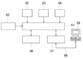
図6は直流成分レベルの状態、交流成分レベルの状態、データ信号からクロック成分を抽出し同期が取れたか否かの情報を外部端末に伝送する機構の構成図を示しており、直流成分レベルの状態、交流成分レベルの状態、データ信号からクロック成分を抽出し同期が取れたか否かの情報を解析するCPU51には、直流成分レベル検波部52、交流成分レベル検波部53、クロック抽出部54、時計55の出力が接続されている。更に、CPU51には例えばフラッシュROM、RAM等から成るデータ保存部56及び通信ドライバ57が接続されている。
【0036】
また、通信ドライバ57には通信回線58を介して遠隔地に置かれた例えばパーソナルコンピュータ等から成る状態表示用の端末機59が接続されている。また通信ドライバ57と端末機59間の通信回線には、ネットワーク又はRS−232C等のローカル接続である。この時計55はCPU51に内蔵することもできる。
【0037】
直流成分レベル検波部52において検出された受信した光信号の直流成分レベル情報はCPU51に出力され、同様に交流成分レベル検波部53で検出された受信した光信号の交流成分レベル情報、クロック抽出部54において検出されたデータの再生成が行えたか否かの情報もCPU51に出力される。CPU51は直流成分レベル検波部52、交流成分レベル検波部53、クロック抽出部54から各情報が変化した場合、つまり正常から異常、又は異常から正常に変化すると時計55から現在時刻を読み出し、状態が変化した項目の情報と発生時刻をデータ保存部56に保存する。
【0038】
CPU51は直流成分レベル検波部52、交流成分レベル検波部53、クロック抽出部54から各情報が変化したことを検知すると変化した項目の情報と発生時刻から所定のフォーマットに基づいてデータ列を作成し、作成したデータ列を通信ドライバ57に送信する。データ列を受け取った通信ドライバ57は、通信回線58を介してCPU51から受け取ったデータ列を端末機59に送信する。
【0039】
また、端末機59の使用者は受信した光信号の直流成分レベルの状態、受信した光信号の交流成分レベルの状態、データ信号からクロック成分を抽出し同期が取れたか否かの情報及びデータ保存部56に保存した情報の何れかの取得要求をする場合には、通信回線58を介して所定のフォーマットに基づいた情報取得要求を通信ドライバ57に送信する。通信ドライバ57は端末機59からの情報取得要求を受け取ると、CPU51にこの情報取得要求を送信する。
【0040】
CPU51はこの情報取得要求を受信すると、受信した情報取得要求が受信した光信号の直流成分レベルの状態、受信した光信号の交流成分レベルの状態、データ信号からクロック成分を抽出し同期が取れたか否かの情報及びデータ保存部56に保存した何れの情報かを識別する。受信した光信号の直流成分レベルの状態の場合には、直流成分レベル検波部52から受信した光信号の直流成分レベルの情報を入手し、受信した光信号の交流成分レベルの状態の場合には、交流成分レベル検波部53から受信した光信号の交流成分レベルの情報を入手し、データ信号からクロック成分を抽出し同期が取れたか否かの情報の場合はクロック抽出部54からデータ信号中のクロック成分を抽出し同期が取れたか否かの情報を入手し、データ保存部56に保存した情報の場合にはデータ保存部56から保存した情報を入手して、入手した情報から所定のフォーマットに基きデータ列を作成し、この作成したデータ列を通信ドライバ57に送信する。データ列を受け取った通信ドライバ57は、通信回線58を介してデータ列を端末機59に送信する。
【0041】
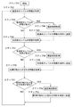
図7は状態変化時の通信シーケンスのフローチャート図を示す。先ず、ステップ41において本シーケンスが開始されると、ステップ42において、直流成分レベル検波部52により受信した光信号の直流成分レベルの情報を取得しステップ43に移る。ステップ43に移ると受信した光信号の直流成分レベルの状態が変化した場合、つまり正常状態から異常状態、又は異常状態から正常状態に変化するとステップ44に移り、時計55から現在時刻を取得し、ステップ45に移り現在時刻と受信した直流成分レベルの情報を端末機59に送信しステップ46に移る。
【0042】
ステップ43において、受信した光信号の直流成分レベルの状態が変化していないと判断された場合にはステップ46に移る。このステップ46においては直流成分レベル検波部52により受信した光信号の交流成分レベルの情報を取得し、ステップ47に移る。ステップ47に移ると受信した光信号の交流成分レベルの状態が変化した場合、つまり正常状態から異常状態、又は異常状態から正常状態に変化するとステップ48に移り、時計55から現在時刻を取得しステップ49に移り、現在時刻と受信した交流成分レベルの情報を端末機59に送信し、ステップ50に移る。
【0043】
また、ステップ47で受信した光信号の交流成分レベルの状態が変化していないと判断された場合はステップ50に移る。ステップ50では、クロック抽出部54によりデータ信号からクロック成分を抽出し同期が取れたか否かの情報を取得してステップ51に移り、クロック成分が抽出した同期が取れたか否かの状態の変化を判断する。クロック成分の同期の状態が変化した場合、つまり正常状態から異常状態、又は異常状態から正常状態に変化した場合にはステップ52に移り、時計55から現在時刻を取得し、ステップ53の処理で現在時刻とデータ信号からクロック成分を抽出し同期が取れたか否かの状態を端末機59に送信しステップ42に戻り、以下このシーケンスを繰り返す。また、ステップ51において、状態の変化がなかった場合においてもステップ42に戻り、以下このシーケンスを繰り返す。
【0044】
図8は端末機から情報取得要求を受信した際のシーケンスのフローチャート図である。ステップ61において、端末機59からの情報取得要求を受信するとステップ62に移り、受信した情報取得要求が、受信した光信号の直流成分レベルの情報取得要求か否かを判断する。直流成分レベルの情報取得要求の場合にステップ63に移り、受信した光信号の直流成分レベルの情報を取得し、ステップ64においてステップ63で取得した光信号の直流成分レベルの情報を端末機59に送信しステップ65に移る。また、ステップ62において端末機59から受信した情報取得要求が、受信した光信号の直流成分レベルの情報取得要求でない場合にはステップ65に移る。
【0045】
ステップ65では端末機59から受信した情報取得要求が、受信した光信号の交流成分レベルの情報取得要求か否かを判断する。交流成分レベルの情報取得要求の場合にはステップ66に移り、受信した光信号の交流成分レベルの情報を取得し、ステップ67においてステップ66で取得した光信号の交流成分レベルの情報を端末機59に送信しステップ68に移る。また、ステップ65において受信した情報取得要求が、受信した光信号の交流成分レベルの情報取得要求でない場合にはステップ68に移る。
【0046】
ステップ68では端末機59から受信した情報取得要求が、データ信号からクロックを抽出し同期が取れたか否かの情報取得要求か否かを判断する。同期が取れたか否かの情報取得要求の場合には、ステップ69に移りデータ信号からクロックを抽出し同期が取れたか否かの情報を取得し、ステップ70においてステップ69で取得したデータ信号からクロックを抽出し同期が取れたか否かの情報を端末機59に送信しステップ71に移る。また、ステップ68の処理で受信した情報取得要求が、データ信号からクロックを抽出し同期が取れたか否かの情報取得要求でない場合はステップ71に移る。
【0047】
ステップ71では、端末機59から受信した情報取得要求が保存したログ情報取得要求か否かを判断する。ログ情報取得要求の場合にはステップ72に移り、保存したログ情報を取得し、ステップ73に移りステップ72で取得した保存したログ情報を端末機59に送信しステップ74に移り、本シーケンスを終了する。また、ステップ71の処理で受信した情報取得要求が、保存したログ情報取得要求でない場合においてもステップ74に移り、本シーケンスを終了する。
【0048】
【発明の効果】
以上説明したように本発明に係る光空間伝送装置は、光空間伝送装置において、異常発生個所を迅速に特定することができ、またこの異常発生、正常復帰情報をログとして保存することにより、後から光空間通信間の通信異常の原因究明を行うことができる。更に、これらの情報を遠隔地に送ることにより、サービスマン、ユーザが光空間伝送装置から離れた場所から異常の原因究明を行うことができる。
【0049】
ここで、対向装置から受信した光信号の直流成分レベルが異常の場合は、光空間通信で異常が発生したと判断できるため、対向装置から光信号が出力されていない、対向装置の光信号出射方向が正しくない、受信装置の光信号入射方向が正しくない、光無線通信経路に天候悪化を含む遮蔽物がある等の原因が考えられ、光空間無線上で異常が発生したことが分かる。
【0050】
対向装置から受信した光信号の交流成分レベルが異常の場合は、対向装置に伝送データが入力されていないことが原因であると考えられ、伝送データを出力している装置間のインタフェ−スに異常が発生したことが分かる。
【0051】
データ信号からクロック成分を抽出できず同期がとれなかった場合は、送られてくるデータのクロック周波数に問題があると考えられるために、対向装置に入力された伝送データが正しくない、又は対向装置に入力された伝送データのデータ速度が正しくないことが原因であると考えられ、対向装置に伝送データを出力している装置に異常が発生したことが分かる。これにより、使用者が異常個所が何処であるかを判断でき、不必要なサービスマンの呼び出しが軽減し、エラーレート測定器等の特別な器材の必要が無いためサービスマンの負荷が軽減される。また、一目で異常個所を特定できるため迅速な対応が実施でき、これにより異常発生から復旧までの時間を最小限に押さえることができる。
【0052】
更に、上記の情報が変化したときにその情報を発生時刻と共に保存する。この機能により、何時どこで異常が発生したかを後で検証でき、異常原因の究明及び対策を迅速に行えるようになる。
【0053】
また、上記情報及び前記保存した情報を外部端末に伝送する機能を有するので、この機能により受信装置のある所まで行かなくても遠隔地で通信異常の状態を知ることができ、サービスマン等が遠隔地から光空間通信装置の状況を知り、その情報から迅速に適切な対応を行うことができる。
【図面の簡単な説明】
【図1】光空間伝送装置の構成図である。
【図2】クロック抽出部の構成図である。
【図3】異常個所の検出及び表示のシーケンスのフローチャート図である。
【図4】ログ情報を保存するシステムの構成図である。
【図5】ログ情報保存シーケンスのフローチャート図である。
【図6】情報を外部端末に伝送する機構の構成図である。
【図7】状態変化時の通信シーケンスのフローチャート図である。
【図8】情報取得要求を受信した際のシーケンスのフローチャート図である。
【符号の説明】
1 送信装置
2 受信装置
3 主信号入力部
4 補助信号発生部
5 合波部
6 電気/光変換部
7 レーザー駆動回路
8 レーザーダイオード
9、10、11、12、13、14 レンズ
15 光/電気変換部
16 受光素子
17 受光回路
18 増幅部
19 補助信号抽出用フィルタ
20 主信号抽出用フィルタ
21 クロック抽出部
22 波形整形部
23 補助信号検波部
24 主信号検波部
25 CPU
26 表示部
27 信号出力部[0001]
BACKGROUND OF THE INVENTION
The present invention relates to an optical space transmission apparatus that transmits information to a remote place by optical radio.
[0002]
[Prior art]
An optical space transmission device modulates a transmission signal into an optical signal on the transmission side, transmits this optical signal in the atmospheric space toward the reception side, and demodulates the optical signal from the transmission side on the reception side. This is an apparatus for transmitting information signals through the atmospheric space.
[0003]
However, the light beam in the optical space transmission device is affected by the attenuation of rain, fog, etc. in the air that is the transmission path, and transmission becomes uneasy, so the optical communication device can communicate normally. As a guide for determining whether or not there is a device that displays only the direct current component level of light necessary to determine whether or not light transmitted from the opposite device is received, is widely known.
[0004]
[Problems to be solved by the invention]
However, the light beam in the above-described optical space transmission device is affected by attenuation due to the influence of rain, fog, etc. in the air that is the transmission path, and transmission abnormalities cause communication abnormalities. In fact, even if there is no abnormality in the optical space communication, it is often questioned that an abnormality has occurred in the optical space communication. Furthermore, it is necessary to call a service man each time an abnormality occurs to check whether an abnormality has occurred in optical wireless communication.
[0005]
In addition, since the optical space transmission apparatus described above displays only the direct current component level of light, it is not possible to determine the location of the abnormality by itself, and if a communication abnormality occurs, is the optical space communication normal? In order to confirm whether or not, it is necessary to temporarily stop communication, connect an error rate measuring device or the like to the optical space communication device, and confirm whether or not an error has occurred.
[0006]
However, optical space transmission devices are often installed at two remote locations, and when detecting an abnormal location as described above, both service personnel must communicate and detect the abnormal location. In addition, a large amount of time and special equipment are required to detect an abnormal part, such as using special equipment such as an error rate measuring device. However, this method requires two or more service personnel and special equipment such as an error rate measuring device for each occurrence of an abnormality, and therefore requires a great load for handling the service.
[0007]
In addition, this type of optical space transmission device is often used for 24 hours, and prompt recovery is required. However, in the above-described method, it takes time to detect an abnormal part, so that recovery is delayed and the operation rate of optical wireless communication is delayed. Is the cause of dropping.
[0008]
Also, because there is no way to know what caused the communication error at this time, if the serviceman rushes to resolve the abnormal condition, the communication will return to normal and an abnormal phenomenon will occur. It becomes very difficult to verify later, and the situation is observed until the next occurrence of abnormality, which causes anxiety to the user. Furthermore, since the state of the optical space communication apparatus can be grasped only after going to the site, a countermeasure must be considered from that point, which also causes a delay in the response.
[0009]
The object of the present invention is to solve the above-mentioned problems, and when an abnormality occurs in optical space communication, the location of the abnormality can be detected at a glance in the receiving unit, and a communication abnormality occurs after the communication abnormality occurs. It is an object of the present invention to provide an optical space transmission device that makes it easy to investigate the cause of the problem and further knows the status of the communication abnormality from a remote location and can investigate the cause of the communication abnormality without going to the site from the information.
[0010]
[Means for Solving the Problems]
In order to achieve the above object, an optical space transmission device according to the present invention is an optical space transmission device that transmits and receives information using an optical wireless device with an opposite device arranged to face each other at a predetermined distance. The optical signal generated by combining the main signal and auxiliary signal From the opposite device Receive A converter for converting into an electric signal, and the electric signal; The auxiliary signal component of the optical signal is extracted from the optical signal by an auxiliary signal extraction filter, and the auxiliary signal component is extracted. DC component level detection means for detecting the DC component level of Said DC component level determination means for determining whether or not the DC component level of the current optical signal is normal from the DC component level, and the electrical signal A main signal component of the optical signal is extracted from the main signal component by a main signal extracting filter, AC component level detection means for detecting the amplitude level of Said AC component level determining means for determining whether the amplitude level of the current main signal component is normal from the amplitude level, clock component extracting means for extracting a clock component from the electrical signal, and the clock component extracting means Synchronization determining means for determining whether or not a clock component has been extracted; and a direct current component level determining means, the alternating current component level determining means, and display means for displaying determination information by the synchronous determining means. It is characterized by.
[0014]
DETAILED DESCRIPTION OF THE INVENTION
The present invention will be described in detail based on the embodiments shown in the drawings.
FIG. 1 is a configuration diagram of an optical space transmission apparatus according to the present embodiment, and includes a
[0015]
A receiving
[0016]
The output of the auxiliary
[0017]
The main signal input to the main
[0018]
The electrical signal amplified by the amplifying
[0019]
The main signal component of the electric signal amplified by the amplifying
[0020]
Further, the electric signal amplified by the amplifying
[0021]
The
[0022]
The electric signal amplified by the amplifying
[0023]
FIG. 2 shows a configuration diagram of the
[0024]
FIG. 3 is a flowchart of the sequence for detecting and displaying an abnormal part. First, when this sequence is started in
[0025]
In
[0026]
If it is determined in
[0027]
If it is determined in step 7 that the AC component level of the light is higher than the prescribed threshold level and is normal, the process proceeds to step 9 where a clock component is extracted from the data signal and it is determined whether or not synchronization is achieved. To do. If synchronization is not achieved and data cannot be regenerated, the process proceeds to step 10. Since it can be determined that there is a problem with the clock frequency of the data to be transmitted in this state, the transmission data input to the opposite device is incorrect, or an abnormality has occurred in which the data rate of the transmission data input to the opposite device is incorrect. Is displayed on the
[0028]
If the clock component is extracted from the data signal in step 9 and the data can be regenerated with synchronization, the process proceeds to step 11 to display on the
[0029]
In FIG. 4, when the state of the direct current component level, the state of the alternating current component level, and the state of whether or not synchronization is obtained by extracting the clock component from the data signal are changed, both the generation time and the change information are stored as log information. The system block diagram for this is shown.
[0030]
The DC component level state, the alternating current component level state, the clock component is extracted from the data signal, and the state of whether or not the synchronization is achieved is analyzed by the
[0031]
DC component level information in the received optical signal detected by the DC component
[0032]
FIG. 6 is a flowchart of the log information storage sequence in FIG. 5. First, when this sequence is started in
[0033]
In
[0034]
In step 30, the AC component
[0035]
FIG. 6 shows a configuration diagram of a mechanism for transmitting a DC component level state, an AC component level state, a clock component from a data signal, and transmitting information about whether synchronization has been established or not to an external terminal. The
[0036]
The
[0037]
DC component level information of the received optical signal detected by the DC component
[0038]
When the
[0039]
In addition, the user of the terminal 59 receives the state of the DC component level of the received optical signal, the state of the AC component level of the received optical signal, information on whether the clock component is extracted from the data signal, and data storage. When making an acquisition request for any of the information stored in the
[0040]
When the
[0041]
FIG. 7 shows a flowchart of a communication sequence when the state changes. First, when this sequence is started in
[0042]
If it is determined in
[0043]
If it is determined in step 47 that the AC component level of the received optical signal has not changed, the process proceeds to step 50. In step 50, the
[0044]
FIG. 8 is a flowchart of a sequence when an information acquisition request is received from a terminal. In step 61, when an information acquisition request from the terminal 59 is received, the process proceeds to step 62, and it is determined whether or not the received information acquisition request is an information acquisition request for the DC component level of the received optical signal. In the case of a DC component level information acquisition request, the process proceeds to step 63, where the DC component level information of the received optical signal is acquired. In step 64, the DC component level information of the optical signal acquired in step 63 is transmitted to the terminal 59. Send to step 65. If the information acquisition request received from the terminal 59 in step 62 is not an information acquisition request for the DC component level of the received optical signal, the process proceeds to step 65.
[0045]
In step 65, it is determined whether or not the information acquisition request received from the terminal 59 is an AC component level information acquisition request for the received optical signal. In the case of an AC component level information acquisition request, the process proceeds to step 66, where AC component level information of the received optical signal is acquired, and in step 67, the AC component level information of the optical signal acquired in step 66 is obtained from the terminal 59. To step 68. If the information acquisition request received in step 65 is not an AC component level information acquisition request for the received optical signal, the process proceeds to step 68.
[0046]
In step 68, it is determined whether or not the information acquisition request received from the terminal 59 is an information acquisition request for extracting a clock from the data signal and synchronizing. In the case of an information acquisition request indicating whether synchronization has been achieved, the process proceeds to step 69 where a clock is extracted from the data signal to acquire information regarding whether synchronization has been achieved, and in step 70, the clock is extracted from the data signal acquired in step 69. Is extracted and information on whether or not synchronization is obtained is transmitted to the terminal 59 and the process proceeds to Step 71. On the other hand, if the information acquisition request received in the process of step 68 is not an information acquisition request indicating whether the clock is extracted from the data signal and synchronized, the process proceeds to step 71.
[0047]
In step 71, it is determined whether the information acquisition request received from the terminal 59 is a stored log information acquisition request. In the case of a log information acquisition request, the process proceeds to step 72, the stored log information is acquired, the process proceeds to step 73, the stored log information acquired in step 72 is transmitted to the terminal 59, the process proceeds to step 74, and this sequence is completed. To do. Further, even when the information acquisition request received in the process of step 71 is not a saved log information acquisition request, the process proceeds to step 74 and this sequence is terminated.
[0048]
【The invention's effect】
As described above, the optical space transmission device according to the present invention can quickly identify the location where an abnormality has occurred in the optical space transmission device. From the above, it is possible to investigate the cause of communication abnormality between optical space communications. Furthermore, by sending these pieces of information to a remote place, it is possible for the service person and the user to investigate the cause of the abnormality from a place away from the optical space transmission device.
[0049]
Here, when the direct current component level of the optical signal received from the opposing device is abnormal, it can be determined that an abnormality has occurred in the optical space communication. Therefore, no optical signal is output from the opposing device. It can be understood that an abnormality has occurred on the optical space radio, for example, because the direction is not correct, the optical signal incident direction of the receiver is not correct, or there is a shielding object including weather deterioration in the optical wireless communication path.
[0050]
If the AC component level of the optical signal received from the opposite device is abnormal, it is considered that the transmission data is not input to the opposite device, and the interface between the devices outputting the transmission data It can be seen that an abnormality has occurred.
[0051]
If the clock component cannot be extracted from the data signal and synchronization is not achieved, it is considered that there is a problem with the clock frequency of the transmitted data, so the transmission data input to the opposite device is incorrect, or the opposite device It can be considered that the cause is that the data rate of the transmission data input to the device is not correct, and it is understood that an abnormality has occurred in the device outputting the transmission data to the opposite device. This makes it possible for the user to determine where the abnormal point is, reducing the need for unnecessary service personnel, and reducing the load on the service personnel because there is no need for special equipment such as an error rate measuring instrument. . In addition, since the location of the abnormality can be identified at a glance, a quick response can be performed, thereby minimizing the time from occurrence of the abnormality to recovery.
[0052]
Further, when the above information changes, the information is stored together with the time of occurrence. This function makes it possible to verify later when and where an abnormality has occurred, and to quickly investigate the cause of the abnormality and take countermeasures.
[0053]
In addition, since it has a function of transmitting the above information and the stored information to an external terminal, it is possible to know the state of communication abnormality at a remote place without going to a place where the receiving device is located, so that a service person can It is possible to know the status of the optical space communication device from a remote location, and to quickly take an appropriate response from the information.
[Brief description of the drawings]
FIG. 1 is a configuration diagram of an optical space transmission apparatus.
FIG. 2 is a configuration diagram of a clock extraction unit.
FIG. 3 is a flowchart of an abnormal part detection and display sequence.
FIG. 4 is a configuration diagram of a system for storing log information.
FIG. 5 is a flowchart of a log information storage sequence.
FIG. 6 is a configuration diagram of a mechanism for transmitting information to an external terminal.
FIG. 7 is a flowchart of a communication sequence when a state changes.
FIG. 8 is a flowchart of a sequence when an information acquisition request is received.
[Explanation of symbols]
1 Transmitter
2 Receiver
3 Main signal input section
4 Auxiliary signal generator
5 multiplexing part
6 Electricity / light conversion part
7 Laser drive circuit
8 Laser diode
9, 10, 11, 12, 13, 14 Lens
15 Optical / electrical converter
16 Light receiving element
17 Light receiving circuit
18 Amplifier
19 Filter for auxiliary signal extraction
20 Main signal extraction filter
21 Clock extractor
22 Waveform shaping part
23 Auxiliary signal detector
24 Main signal detector
25 CPU
26 Display section
27 Signal output section
Claims (3)
主信号と補助信号とを合波することにより生成された光信号を前記対向装置から受信し電気信号に変換する変換部と、
前記電気信号から補助信号抽出用フィルタにより前記光信号の補助信号成分を抽出し、該補助信号成分の直流成分レベルを検出する直流成分レベル検出手段と、
前記直流成分レベルから現在の光信号の直流成分レベルが正常であるか否かを判断する直流成分レベル判断手段と、
前記電気信号から主信号抽出用フィルタにより前記光信号の主信号成分を抽出し、該主信号成分の振幅レベルを検出する交流成分レベル検出手段と、
前記振幅レベルから現在の主信号成分の振幅レベルが正常であるか否かを判断する交流成分レベル判断手段と、
前記電気信号からクロック成分を抽出するクロック成分抽出手段と、
該クロック成分抽出手段により前記クロック成分が抽出できたか否かの判断を行う同期判断手段と、
前記直流成分レベル判断手段、前記交流成分レベル判断手段、前記同期判断手段による判断情報を表示する表示手段と、を有することを特徴とする光空間伝送装置。An optical space transmission device that transmits and receives information using optical wireless with an opposing device arranged to face each other at a predetermined distance,
A conversion unit that receives an optical signal generated by combining the main signal and the auxiliary signal from the opposing device and converts the optical signal into an electrical signal;
DC component level detection means for extracting an auxiliary signal component of the optical signal from the electrical signal by an auxiliary signal extraction filter and detecting a DC component level of the auxiliary signal component ;
A DC component level determination means for DC component level of the current optical signal from the DC component level to determine whether it is normal,
AC component level detection means for extracting a main signal component of the optical signal from the electrical signal by a main signal extraction filter and detecting an amplitude level of the main signal component ;
And AC component level determination means for determining whether the amplitude level of the current main signal component is normal from the amplitude level,
Clock component extraction means for extracting a clock component from the electrical signal;
Synchronization determination means for determining whether or not the clock component could be extracted by the clock component extraction means;
An optical space transmission apparatus comprising: a direct current component level determination means; an alternating current component level determination means; and a display means for displaying determination information by the synchronization determination means.
Priority Applications (1)
| Application Number | Priority Date | Filing Date | Title |
|---|---|---|---|
| JP2000114901A JP4402251B2 (en) | 2000-04-17 | 2000-04-17 | Optical space transmission equipment |
Applications Claiming Priority (1)
| Application Number | Priority Date | Filing Date | Title |
|---|---|---|---|
| JP2000114901A JP4402251B2 (en) | 2000-04-17 | 2000-04-17 | Optical space transmission equipment |
Publications (3)
| Publication Number | Publication Date |
|---|---|
| JP2001298419A JP2001298419A (en) | 2001-10-26 |
| JP2001298419A5 JP2001298419A5 (en) | 2007-06-14 |
| JP4402251B2 true JP4402251B2 (en) | 2010-01-20 |
Family
ID=18626631
Family Applications (1)
| Application Number | Title | Priority Date | Filing Date |
|---|---|---|---|
| JP2000114901A Expired - Fee Related JP4402251B2 (en) | 2000-04-17 | 2000-04-17 | Optical space transmission equipment |
Country Status (1)
| Country | Link |
|---|---|
| JP (1) | JP4402251B2 (en) |
Families Citing this family (4)
| Publication number | Priority date | Publication date | Assignee | Title |
|---|---|---|---|---|
| JP2009071368A (en) * | 2007-09-10 | 2009-04-02 | Toyo Electric Corp | Spatial light transmission apparatus |
| JP2010079450A (en) * | 2008-09-24 | 2010-04-08 | Toyo Electric Corp | Space optical transmission device |
| JP4983870B2 (en) * | 2009-07-24 | 2012-07-25 | Kddi株式会社 | Optical transceiver |
| JP7175931B2 (en) * | 2020-02-25 | 2022-11-21 | アンリツ株式会社 | Measuring device and measuring method |
-
2000
- 2000-04-17 JP JP2000114901A patent/JP4402251B2/en not_active Expired - Fee Related
Also Published As
| Publication number | Publication date |
|---|---|
| JP2001298419A (en) | 2001-10-26 |
Similar Documents
| Publication | Publication Date | Title |
|---|---|---|
| CA2334132C (en) | Method and apparatus for automatically identifying system faults in an optical communications system from repeater loop gain signatures | |
| US7684700B2 (en) | Loss-of-signal detecting device | |
| JP3446211B2 (en) | Detection of self-stimulation signal in optical transmission system | |
| JP3851610B2 (en) | Transmission path loss test method, slave station, master station and communication system using the method | |
| EP2456127A1 (en) | Method, system and apparatus for diagnosing physical downlink failure | |
| JP4402251B2 (en) | Optical space transmission equipment | |
| US5657154A (en) | Monitoring system for all optical regenerators | |
| JPH04235425A (en) | Method and system of remote measurement | |
| JP2005033401A (en) | Optical transmitting/receiving apparatus | |
| US7132646B2 (en) | Signal light interruption detecting method and optical amplifier using same | |
| CN212623123U (en) | Cable detector device capable of dynamically filtering environmental interference | |
| US11316592B2 (en) | Optical module and optical communication system | |
| JP2580738B2 (en) | Fault location device | |
| JP4266491B2 (en) | Optical space transmission equipment | |
| US6501573B1 (en) | Apparatus and method for monitoring the qualities of optical signal using clock amplitude | |
| JP2001298418A (en) | Optical space transmitter | |
| JP2508986B2 (en) | Optical amplification repeater system | |
| JP2000258487A (en) | Slave station, surge detection time evaluation, failure point locating system, and failure point locating method | |
| JPH04301934A (en) | Optical transmitter and optical communication equipment using optical transmitter | |
| KR100321003B1 (en) | Apparatus for distributing synchronization signal using a digital trunk | |
| KR200309696Y1 (en) | Apparatus of Transmitting Optical Signal having Optical Power Meter | |
| JPH05284120A (en) | Optical transmission line monitor method | |
| CN111880225A (en) | Cable detector device and method for dynamically filtering environmental interference | |
| JPH0969805A (en) | Communication system | |
| JP2004112325A (en) | Method and apparatus for detecting fault in communication apparatus |
Legal Events
| Date | Code | Title | Description |
|---|---|---|---|
| A521 | Written amendment |
Free format text: JAPANESE INTERMEDIATE CODE: A523 Effective date: 20070417 |
|
| A621 | Written request for application examination |
Free format text: JAPANESE INTERMEDIATE CODE: A621 Effective date: 20070417 |
|
| A977 | Report on retrieval |
Free format text: JAPANESE INTERMEDIATE CODE: A971007 Effective date: 20080624 |
|
| A131 | Notification of reasons for refusal |
Free format text: JAPANESE INTERMEDIATE CODE: A131 Effective date: 20080701 |
|
| A521 | Written amendment |
Free format text: JAPANESE INTERMEDIATE CODE: A523 Effective date: 20080901 |
|
| A131 | Notification of reasons for refusal |
Free format text: JAPANESE INTERMEDIATE CODE: A131 Effective date: 20090217 |
|
| A521 | Written amendment |
Free format text: JAPANESE INTERMEDIATE CODE: A523 Effective date: 20090416 |
|
| TRDD | Decision of grant or rejection written | ||
| A01 | Written decision to grant a patent or to grant a registration (utility model) |
Free format text: JAPANESE INTERMEDIATE CODE: A01 Effective date: 20091027 |
|
| A01 | Written decision to grant a patent or to grant a registration (utility model) |
Free format text: JAPANESE INTERMEDIATE CODE: A01 |
|
| A61 | First payment of annual fees (during grant procedure) |
Free format text: JAPANESE INTERMEDIATE CODE: A61 Effective date: 20091029 |
|
| R150 | Certificate of patent or registration of utility model |
Free format text: JAPANESE INTERMEDIATE CODE: R150 |
|
| FPAY | Renewal fee payment (event date is renewal date of database) |
Free format text: PAYMENT UNTIL: 20121106 Year of fee payment: 3 |
|
| FPAY | Renewal fee payment (event date is renewal date of database) |
Free format text: PAYMENT UNTIL: 20131106 Year of fee payment: 4 |
|
| LAPS | Cancellation because of no payment of annual fees |