JP4374401B2 - Ultra thin high brightness light panel - Google Patents
Ultra thin high brightness light panel Download PDFInfo
- Publication number
- JP4374401B2 JP4374401B2 JP2005236568A JP2005236568A JP4374401B2 JP 4374401 B2 JP4374401 B2 JP 4374401B2 JP 2005236568 A JP2005236568 A JP 2005236568A JP 2005236568 A JP2005236568 A JP 2005236568A JP 4374401 B2 JP4374401 B2 JP 4374401B2
- Authority
- JP
- Japan
- Prior art keywords
- light
- ultra
- light guide
- guide plate
- intensity
- Prior art date
- Legal status (The legal status is an assumption and is not a legal conclusion. Google has not performed a legal analysis and makes no representation as to the accuracy of the status listed.)
- Expired - Fee Related
Links
Images


Description
この発明は、交流電源で超高輝度LEDを点灯し、表示用フィルムの照明が均一の明るさで高輝度に形成される超薄型高輝度ライトパネルに関する。 The present invention relates to an ultra-thin high-intensity light panel in which an ultra-high-brightness LED is turned on with an AC power source, and illumination of a display film is formed with high brightness and uniform brightness.
文字,絵柄,映像等のパターンを拡散表示する手段として、例えば、カッティングシートや表示用フィルムを凹凸のある透明板に貼着するものや、前記カッティングシートや表示用フィルムを有機又は無機のELに貼着して照明するものがある。また、最近ではELを照光体として使用するものもある。なお、この発明に関連する公知技術として「特許文献1」が挙げられる。
前記従来技術や前記公知技術はいずれもカッティングシートや表示用フィルムを拡散表示することは可能であるが、その輝度が不十分であり、かつ画面の明るさが均一にならない問題点がある。また、全体の厚みも薄型とならず高重量のものとなる。また、交流電源と連結する場合にはインバータが別に必要となり持ち運びやセッティングが面倒であり、全体としてコンパクトにまとめられぬ問題点がある。また、ELは現在のところ、高価であり、手軽に使用できない。Although both the conventional technique and the known technique can diffusively display a cutting sheet or a display film, there are problems in that the luminance is insufficient and the brightness of the screen is not uniform. Also, the overall thickness is not thin but heavy. In addition, when connecting to an AC power source, an inverter is required separately, which is troublesome to carry and set, and there is a problem that cannot be compacted as a whole. In addition, EL is at present, are expensive, it can not be used easily.
この発明は、以上の問題点を解決するものであり、外付きインバータを用いることなく超高輝度LEDを照射でき、画面全体を均一に、かつ超高輝度拡散表示でき、薄型で軽量で取り扱い性がよく高寿命の超薄型高輝度ライトパネルを提供することを目的とする。 The present invention solves the above-described problems, and can irradiate an ultra-bright LED without using an external inverter, and can uniformly and super-brightly display the entire screen, is thin, lightweight and easy to handle. An object of the present invention is to provide an ultra-thin high-intensity light panel that has a long lifetime.
この発明は、以上の目的を達成するために、請求項1の発明は、放熱性を有する材料からなる枠体と、前記枠体内に着脱可能に収納される画像表示部と、
前記画像表示部を照明すべく前記枠体内に保持される超高輝度LEDと、
前記超高輝度LEDと電源との間に介設され前記枠体に保持されるLED点灯用回路部とを備えるライトパネルであって、
前記画像表示部は、合成樹脂製の光拡散用導光板と、前記光拡散用導光板の表面または裏面の少なくとも一方に配置される表示用フィルム及び反射板とからなり、前記光拡散用導光板は、光の入出方向に沿って並設される多数本の線体の群を板の表面または裏面の少なくとも一方に刻設し、前記線体は、その幅寸法及び深さ寸法を光の入力方向から中心に向かって拡寸し、前記線体には、点状レーザ加工体を光の入力端から中心に向かって密に形成したことを特徴とする。In order to achieve the above object, the present invention provides a frame body made of a material having a heat dissipation property, an image display unit detachably housed in the frame body,
An ultra-bright LED held in the frame to illuminate the image display;
A light panel comprising an LED lighting circuit unit interposed between the ultra-bright LED and a power source and held by the frame;
The image display unit includes a light guide plate for light diffusion made of synthetic resin, and a display film and a reflective plate disposed on at least one of the front surface and the back surface of the light guide plate for light diffusion, and the light guide plate for light diffusion Engraves a group of a large number of linear bodies arranged side by side along the light entering / exiting direction on at least one of the front surface and the back surface of the plate, and the linear body has its width dimension and depth dimension input to the light. The size is increased from the direction toward the center, and the pointed laser processed body is densely formed on the linear body from the light input end toward the center.
また、請求項2の発明は、前記光拡散用導光板の周縁を鏡面仕上げし、前記超高輝度LEDを配置しない前記周縁には反射材を配置したことを特徴とする。Further, the invention of
また、請求項3の発明は、前記超高輝度LEDの周縁に反射材を配置したことを特徴とする。
また、請求項4の発明は、複数の前記光拡散用導光板を前記線体の群が対峙するように配設し、
その間に前記反射板を介設することを特徴とする。Further, the invention of
In the invention of
In the meantime, the reflection plate is interposed.
また、請求項5の発明は、複数の前記光拡散用導光板を並設し、その一方の前記光拡散用導光板の前記線体の群の側に反射板を配置し、
他方の前記光拡散用導光板の前記線体の群のない平面側に前記表示用フィルムを配置することを特徴とする。In the invention of
The display film is arranged on a flat surface side of the other light diffusion light guide plate without the group of the linear bodies.
また、請求項6の発明は、隣接する前記光拡散用導光板の前記線体の群が互いに直交して配置されることを特徴とする。 The invention of
また、請求項7の発明は、前記光拡散用導光板と前記反射板との間には、光拡散板が介設されることを特徴とする。 The invention of
この発明の請求項1の超薄型高輝度ライトパネルによれば、交流電源に直接連結されて照光する超高輝度LEDにより画像表示部が超高輝度に照射されると共に、画像表示部を構成する特殊加工の光拡散用導光板により、表示用フィルムは均一の照度で拡散されて超高輝度に照明される。また、画像表示部を構成する板材は薄型で軽量にでき、交換可能であり、持ち運びやメンテナンスや取り扱い性や保管が極めて容易にできる。また、LEDを使用するため高寿命である。 According to the ultra-thin high-intensity light panel of the first aspect of the present invention, the image display unit is irradiated with ultra-high luminance by the ultra-high luminance LED that is directly connected to the AC power source and illuminates, and the image display unit is configured. Due to the specially processed light diffusion light guide plate, the display film is diffused with uniform illuminance and illuminated with ultra-high brightness. Further, the plate material constituting the image display unit can be thin and lightweight, and can be exchanged, and can be carried, maintained, handled, and stored very easily. Moreover, since the LED is used, it has a long life.
また、請求項2乃至請求項5の発明によれば、光拡散性を一層向上させることができ、極めて明るいフィルム表示ができる。 Moreover, according to the invention of
また、請求項6の超薄型高輝度ライトパネルによれば、光拡散板を介設することにより、光拡散度を更に向上することができ、一層明るい画面表示が可能となる。 According to the ultrathin high-intensity light panel of
以下、この発明の超薄型高輝度ライトパネルの実施の形態を図面を参照して詳述する。
図1乃至図5はこの発明の「実施例1」を示し、図7はこの発明の実施例2を示す。Embodiments of an ultra-thin high-intensity light panel according to the present invention will be described in detail below with reference to the drawings.
1 to 5 show "
図1は、この発明の超薄型高輝度ライトパネルの全体構造の概要を示すものである。超薄型高輝度ライトパネル100は、放熱性がよく軽量の材料、例えば、アルミニウム材からなる枠体3とこの内部に収納される画像表示体4と、枠体内に保持される超高輝度LED5と、交流電源7と超高輝度LED5との間に介設されて枠体3内に保持されるLED点灯用回路部6等とからなる。なお、交流電源7は100Vのものでよく、外付きのインバータは不要である。また、この実施例では超高輝度LED5は枠体3の上下に配置され、LED点灯用回路部6は枠体3の左右に配置されるが、これに限定するものではない。 FIG. 1 shows an outline of the overall structure of an ultra-thin high-intensity light panel according to the present invention. The ultra-thin high-
枠体3は、超高輝度LED5やLED点灯用回路部6を内部保持する空間8を形成すると共に画像表示部4を着脱可能に保持する保持部9等を形成し、例えば、上下左右部材が夫々分離できる四角形の枠からなる。アルミニウム材からなるため、極めて軽量であり放熱性もよい。 The
画像表示部4は、アクリル樹脂製の光拡散用導光板1と、この表面に当接して配置される表示用フィルム10と、裏面に当接して配置される反射板11とからなる。なお、反射板11は公知技術のものが適用され、表示用フィルム10は任意のものでよい。光拡散用導光板1はこの発明の主要構成要素であり、その詳細構造は後述する。 The
超高輝度LED5は、前記のように枠体3の上下枠内に多数個並設されるものからなり、その数は画像表示部4の大きさや種類によって決められる。単一の超高輝度LED5及びそのまわりの各部材の詳細構造が図3に示される。即ち、LED本体5aは透明な保護カバー5gにより保護され、LED本体5aは導伝性絶縁ゴムのLEDマウント部5bを介してLEDプリント基板5cに支持される。このLEDプリント基板5cはLED点灯用回路部6に連結される。また、アルミ材の放熱体5dにより支持され、この放熱体5dは絶縁材5eにより枠体3に保持される。また、LED本体5aを被包する保護カバー5gのまわりには反射材5fが配置される。また、枠体3内にはLEDプリント基板に連結される配線5hが収納される。As described above, a large number of
交流電源7に直接連結されるLED点灯用回路部6は、交流電源7からの交流を超高輝度LED5を照射するに必要な低ボルトの直流にする構造のものからなり、特殊の回路からなるが、例えば、特許第3122870号に開示されている「交流用LED点灯回路」の如きものが採用される。なお、この実施例では、このLED点灯用回路部6は枠体の左右枠内に収納されるが、その収納数は画面表示部4の大きさに対応して決められる。 The LED
以上の構成により、交流電源7より、例えば、100Vの電源を入力すると、LED点灯用回路部6によって入力電流が制御され、超高輝度LED5を点灯し得る低電圧で略直流に近い電力が出力されて超高輝度LED5が点灯し、画像表示部4が照明される。具体的には超高輝度LED5の光は光拡散用導光板1に入力され、その拡散光が直接及び反射板11を介して表示用フィルム10に導入されて表示用フィルム10を超高輝度に、かつ均一に照明することになる。なお、表示用フィルム10は所望のものに交換できるため、任意の表示用フィルムを照明することができる。また、その他の構成要素も交換可能であり、全体として長期間使用することができる。なお、図2に示すように表示用フィルム10は透明補護板12により保持され、反射板11は補強板13により保持される。With the above configuration, for example, when a 100 V power source is input from the
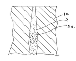
次に、この発明の超薄型高輝度ライトパネル100の主要構成要素である光拡散用導光板1の形状を、図4、図5及び図6により説明する。光拡散用導光板1は、例えば、アクリル樹脂からなる四角状の平板体1aと、これに例えば、レーザ加工により刻設された多 数本の線体2の群からなる。この線体2は超高輝度LED5のある側(一端部)から他端側に向かって形成されるほぼ直線状の線体からなり、夫々の線体2は並設される。なお、各線体2は基本的に同形状であるが、相異形状であってもよい。また、線体2は板の表面のみでなく、裏面にも刻設されてもよい。なお、反射板11は光拡散用導光板1の線体2側に配設される。Next, the shape of the light diffusing
図5(a),(b)は線体2の詳細構造を模式的に拡大表示したものである。線体2は一端側にあって幅wで深さtのものからなり、平板体1aの中心部において幅W(W>w)で深さT(T>t)のものからなる。即ち、線体2は幅wから幅Wと拡寸して形成されると共に深さtから深さTへと拡寸して形成される。この場合、幅寸法のwやW及び深さ寸法tやTのサイズについては平板体1aの大きさや各構成要素の機能,大きさ,形状等を勘案して経験的、実験的に決める。以上により、一端部の超高輝度LED5から入力された光は平板体1aのすべての場所において均一の拡散光となり、表示用フィルム10を均一に、かつ超高輝度に照明することになる。FIGS. 5A and 5B are schematic enlarged views of the detailed structure of the
図5(a),(b)により線体2の形状を説明したが、線体2は更に図6に示す加工が施されている。即ち、線体2の刻設されている表面にはレーザ加工による点状レーザ加工体2aが点状に形成される。この点状レーザ加工体2aは超高輝度LED5の配置されている線体2の一端側から中心に向かって次第に密になるように加工される。この密の程度や変化は経験的及び実験的に決められる。この点状レーザ加工体2aを刻設することにより、より均一の拡散光となり、明るさの向上が図れる。 Although the shape of the
光拡散用導光板1は図7(a)に示すようにその周縁がすべて鏡面加工したものからなる。これにより超高輝度LED5からの光の透過度の向上を図る。また、図7(b)に示すように、光拡散用導光板1の周縁で超高輝度LED5の配設されている側以外の周縁には反射材5fが設けられる。これにより、光拡散度の向上が図れる。As shown in FIG. 7A, the light diffusing
図8は2枚板の光拡散用導光板1,1を用いた実施例である。この光拡散用導光板1,1はその線体2を互いに対峙した状態で配置され、その間に反射板11が介設されたものである。なお、この場合表示用フィルム10は光拡散用導光板1,1の平面側に配置される。以上により、一層明るい表示が可能になる。 FIG. 8 shows an embodiment using two
図9は2枚の光拡散用導光板1,1を同じ方向に隣接して配置した実施例である。この場合、反射板11は一方側の光拡散用導光板1の線体2に接して配置され、表示用フィルム10は他方の光拡散用導光板1の平面側に接して配置される。以上により一層明るい表示が可能になる。 FIG. 9 shows an embodiment in which two light diffusion
図10は2枚の光拡散用導光板1,1の線体2を互いに直交して配置したものであり更に一層の明るい表示が可能である。 FIG. 10 shows two light diffusing
実施例2乃至4は一対の光拡散用導光板1について説明したが、光拡散用導光板1は2枚に限定するものではない。 In the second to fourth embodiments, the pair of light diffusing
実施例1の超薄型高輝度ライトパネル100は光拡散用導光板1に反射板11が直接当接した状態で配置されるものであるが、図11に示すように実施例5の超薄型高輝度ライトパネル100aは光拡散用導光板1と反射板11との間に拡散板14を介設したものからなる。これによる拡散度をより向上させることが可能になる。また、拡散板12も光拡散用導光板1の機能により、不要となる場合も勿論ある。 The ultra-thin high-intensity
この発明の超薄型高輝度ライトパネル100,100aは照明を必要とする各種の表示用フィルムのすべてに適用され、例えば、宣伝広告用,安全保護用,道路標識,各種看板等あらゆる表示体に適用され、その利用範囲は極めて広い。 The ultra-thin high-
1 光拡散用導光板
1a 平板体
2 線体
2a 点状レーザ加工体
3 枠体
4 画像表示部
5 超高輝度LED
5a LED本体
5b LEDマウント部
5c LEDプリント基板
5d 放熱体
5e 絶縁体
5f 反射材
5g 保護カバー
5h 配線
6 LED点灯用回路部
7 交流電源
8 空間
9 保持部
10 表示用フィルム
11 反射板
12 透明補護板
13 補強板
14 拡散板
100 超薄型高輝度ライトパネル
100a 超薄型高輝度ライトパネルDESCRIPTION OF
5a LED body 5b LED mount part 5c LED printed circuit board 5d Heat sink 5e Insulator 5f Reflective material
Claims (7)
前記枠体内に着脱可能に収納される画像表示部と、
前記画像表示部を照明すべく前記枠体内に保持される超高輝度LEDと、
前記超高輝度LEDと電源との間に介設され前記枠体に保持されるLED点灯用回路部とを備えるライトパネルであって、
前記画像表示部は、
合成樹脂製の光拡散用導光板と、
前記光拡散用導光板の表面または裏面の少なくとも一方に配置される表示用フィルム及び反射板とからなり、
前記光拡散用導光板は、光の入出方向に沿って並設される多数本の線体の群を板の表面または裏面の少なくとも一方に刻設し、
前記線体は、その幅寸法及び深さ寸法を光の入力方向から中心に向かって拡寸し、
前記線体には、点状レーザ加工体を光の入力端から中心に向かって密に形成したことを特徴とする超薄型高輝度ライトパネル。A frame made of a heat-dissipating material;
An image display unit detachably housed in the frame;
An ultra-bright LED held in the frame to illuminate the image display;
A light panel comprising an LED lighting circuit unit interposed between the ultra-bright LED and a power source and held by the frame;
The image display unit
A light guide plate for light diffusion made of synthetic resin;
It consists of a display film and a reflector arranged on at least one of the front surface or the back surface of the light diffusion light guide plate,
The light diffusion light guide plate is formed by engraving a group of a plurality of linear bodies arranged in parallel along the light entering / exiting direction on at least one of the front surface or the back surface of the plate,
The linear body expands its width dimension and depth dimension from the light input direction toward the center,
An ultra-thin, high-intensity light panel, wherein the line-shaped body is formed by densely forming a dotted laser processed body from the light input end toward the center.
前記超高輝度LEDを配置しない前記周縁には反射材を配置したことを特徴とする請求項1に記載の超薄型高輝度ライトパネル。The peripheral edge of the light diffusing light guide plate is mirror finished,
The ultra-thin high-intensity light panel according to claim 1, wherein a reflective material is disposed on the peripheral edge where the ultra-high-intensity LEDs are not disposed.
その間に前記反射板を介設することを特徴とする請求項1乃至請求項3のいずれか1項に記載の超薄型高輝度ライトパネル。A plurality of the light diffusing light guide plates are arranged so that the groups of the wire bodies face each other;
The ultra-thin high-intensity light panel according to any one of claims 1 to 3, wherein the reflection plate is interposed therebetween.
他方の前記光拡散用導光板の前記線体の群のない平面側に前記表示用フィルムを配置することを特徴とする請求項1乃至請求項4のいずれか1項に記載の超薄型高輝度ライトパネル。A plurality of the light diffusing light guide plates are arranged side by side, and a reflecting plate is disposed on the group side of the linear body of the one light diffusing light guide plate,
5. The ultra-thin high structure according to claim 1, wherein the display film is arranged on a flat surface side of the other light diffusion light guide plate without the group of the linear bodies. Luminance light panel.
Priority Applications (1)
| Application Number | Priority Date | Filing Date | Title |
|---|---|---|---|
| JP2005236568A JP4374401B2 (en) | 2005-03-09 | 2005-08-17 | Ultra thin high brightness light panel |
Applications Claiming Priority (2)
| Application Number | Priority Date | Filing Date | Title |
|---|---|---|---|
| JP2005065178 | 2005-03-09 | ||
| JP2005236568A JP4374401B2 (en) | 2005-03-09 | 2005-08-17 | Ultra thin high brightness light panel |
Publications (3)
| Publication Number | Publication Date |
|---|---|
| JP2006285181A JP2006285181A (en) | 2006-10-19 |
| JP2006285181A5 JP2006285181A5 (en) | 2007-03-22 |
| JP4374401B2 true JP4374401B2 (en) | 2009-12-02 |
Family
ID=37407140
Family Applications (1)
| Application Number | Title | Priority Date | Filing Date |
|---|---|---|---|
| JP2005236568A Expired - Fee Related JP4374401B2 (en) | 2005-03-09 | 2005-08-17 | Ultra thin high brightness light panel |
Country Status (1)
| Country | Link |
|---|---|
| JP (1) | JP4374401B2 (en) |
Cited By (1)
| Publication number | Priority date | Publication date | Assignee | Title |
|---|---|---|---|---|
| CN103443671A (en) * | 2011-01-25 | 2013-12-11 | 皇家飞利浦有限公司 | Mosaic lighting device with transparent body with a plurality of light guides delimited by slits |
Families Citing this family (3)
| Publication number | Priority date | Publication date | Assignee | Title |
|---|---|---|---|---|
| KR101410496B1 (en) | 2007-11-08 | 2014-06-20 | 삼성디스플레이 주식회사 | Light source module, back light assembly having the light source module and display apparatus having the back light assembly |
| KR101519331B1 (en) * | 2008-02-18 | 2015-05-13 | 삼성디스플레이 주식회사 | Backlight assembly and display device having same |
| KR101535926B1 (en) | 2008-08-12 | 2015-07-13 | 삼성디스플레이 주식회사 | Light emitting diode backlight assembly and liquid crystal display thereof |
-
2005
- 2005-08-17 JP JP2005236568A patent/JP4374401B2/en not_active Expired - Fee Related
Cited By (2)
| Publication number | Priority date | Publication date | Assignee | Title |
|---|---|---|---|---|
| CN103443671A (en) * | 2011-01-25 | 2013-12-11 | 皇家飞利浦有限公司 | Mosaic lighting device with transparent body with a plurality of light guides delimited by slits |
| CN103443671B (en) * | 2011-01-25 | 2016-06-22 | 皇家飞利浦有限公司 | There is the mosaic luminaire of transparent body with the multiple photoconductions demarcated by slit |
Also Published As
| Publication number | Publication date |
|---|---|
| JP2006285181A (en) | 2006-10-19 |
Similar Documents
| Publication | Publication Date | Title |
|---|---|---|
| US20120140448A1 (en) | Backlight device and image display using the same | |
| JP2009295560A (en) | Planar light source and liquid crystal display device | |
| JP2010009785A (en) | Hollow type surface lighting device | |
| KR20180125953A (en) | Light emitting device, display device and lighting device | |
| JP2010170898A (en) | Edge light type partial drive backlight unit and liquid crystal display | |
| JP2009042360A (en) | Illumination light display device | |
| JP3122411B2 (en) | Edge light panel light source device | |
| JP2012204336A (en) | Illumination device and display device | |
| JPH11353920A (en) | Multicolor light emitting surface light source unit | |
| JP4374401B2 (en) | Ultra thin high brightness light panel | |
| CA2621124C (en) | Edge mounted led array backlight for flat panel display | |
| JP2005251687A (en) | Surface lighting device | |
| JP2006285181A5 (en) | ||
| US8596854B2 (en) | Light-guide module | |
| JP2010021073A (en) | Illumination device and liquid crystal display device using same | |
| KR20110020055A (en) | Backlight unit | |
| JP2010231964A (en) | Lighting device | |
| JPH1114835A (en) | Light emission display plate | |
| JPH11133425A (en) | Illuminator for liquid crystal panel | |
| TWM312683U (en) | Improvement structure of light source of backlight module of liquid crystal display | |
| JP2006032103A (en) | Surface light source device and image display device | |
| JP4324006B2 (en) | Surface illumination element | |
| JP2005050630A (en) | Double-sided planar light emitting source | |
| JP3181799U (en) | Illumination device | |
| JP2917866B2 (en) | LED surface light source |
Legal Events
| Date | Code | Title | Description |
|---|---|---|---|
| A521 | Written amendment |
Free format text: JAPANESE INTERMEDIATE CODE: A523 Effective date: 20051026 |
|
| A621 | Written request for application examination |
Free format text: JAPANESE INTERMEDIATE CODE: A621 Effective date: 20061127 |
|
| A521 | Written amendment |
Free format text: JAPANESE INTERMEDIATE CODE: A523 Effective date: 20070118 |
|
| A621 | Written request for application examination |
Free format text: JAPANESE INTERMEDIATE CODE: A621 Effective date: 20070118 |
|
| RD02 | Notification of acceptance of power of attorney |
Free format text: JAPANESE INTERMEDIATE CODE: A7422 Effective date: 20070118 |
|
| A871 | Explanation of circumstances concerning accelerated examination |
Free format text: JAPANESE INTERMEDIATE CODE: A871 Effective date: 20080806 |
|
| A975 | Report on accelerated examination |
Free format text: JAPANESE INTERMEDIATE CODE: A971005 Effective date: 20080930 |
|
| A131 | Notification of reasons for refusal |
Free format text: JAPANESE INTERMEDIATE CODE: A131 Effective date: 20081003 |
|
| A521 | Written amendment |
Free format text: JAPANESE INTERMEDIATE CODE: A523 Effective date: 20081128 |
|
| A131 | Notification of reasons for refusal |
Free format text: JAPANESE INTERMEDIATE CODE: A131 Effective date: 20090225 |
|
| A521 | Written amendment |
Free format text: JAPANESE INTERMEDIATE CODE: A523 Effective date: 20081128 |
|
| AA91 | Notification of revocation by ex officio |
Free format text: JAPANESE INTERMEDIATE CODE: A971091 Effective date: 20090324 |
|
| A01 | Written decision to grant a patent or to grant a registration (utility model) |
Free format text: JAPANESE INTERMEDIATE CODE: A01 Effective date: 20090501 |
|
| A61 | First payment of annual fees (during grant procedure) |
Free format text: JAPANESE INTERMEDIATE CODE: A61 Effective date: 20090507 |
|
| R150 | Certificate of patent or registration of utility model |
Free format text: JAPANESE INTERMEDIATE CODE: R150 |
|
| FPAY | Renewal fee payment (event date is renewal date of database) |
Free format text: PAYMENT UNTIL: 20120918 Year of fee payment: 3 |
|
| FPAY | Renewal fee payment (event date is renewal date of database) |
Free format text: PAYMENT UNTIL: 20120918 Year of fee payment: 3 |
|
| FPAY | Renewal fee payment (event date is renewal date of database) |
Free format text: PAYMENT UNTIL: 20120918 Year of fee payment: 3 |
|
| FPAY | Renewal fee payment (event date is renewal date of database) |
Free format text: PAYMENT UNTIL: 20120918 Year of fee payment: 3 |
|
| FPAY | Renewal fee payment (event date is renewal date of database) |
Free format text: PAYMENT UNTIL: 20150918 Year of fee payment: 6 |
|
| LAPS | Cancellation because of no payment of annual fees |