JP4370032B2 - Near-field optical microscope - Google Patents
Near-field optical microscope Download PDFInfo
- Publication number
- JP4370032B2 JP4370032B2 JP2000001026A JP2000001026A JP4370032B2 JP 4370032 B2 JP4370032 B2 JP 4370032B2 JP 2000001026 A JP2000001026 A JP 2000001026A JP 2000001026 A JP2000001026 A JP 2000001026A JP 4370032 B2 JP4370032 B2 JP 4370032B2
- Authority
- JP
- Japan
- Prior art keywords
- light
- probe
- frequency
- incident
- wavelength
- Prior art date
- Legal status (The legal status is an assumption and is not a legal conclusion. Google has not performed a legal analysis and makes no representation as to the accuracy of the status listed.)
- Expired - Fee Related
Links
Images


Description
【0001】
【発明の属する技術分野】
本発明は、近接場光学顕微鏡装置に係り、特に、散乱型探針を利用した近接場光学顕微鏡装置において、入射光波長の変化に応じて信号強度が変化する場合の近接場信号のS/Nを向上させるための手段を備えた近接場光学顕微鏡装置に関する。
【0002】
【従来の技術】
近時、走査型近接場光学顕微鏡(SNOM)は、エバネッセント波を検出することにより回折限界を超吏る分解能を有する光学顕微鏡として、生体試料の蛍光測定や、フォトニクス用材料、素子の評価(誘電体光導波路各種特性評価、半導体量子ドットの発光スペクトルの測定、半導体面発光素子の諸特性の評価など)等への応用をめざして盛んに開発が進められている。
【0003】
このSNOMは、基本的には、試料に光を照射した状態で鋭い探針を近づけ、試料の近傍の光の場(近接場)の状態を検出する装置である。
【0004】
1993年12月21日付けでBetzig等に付与された米国特許第5,272,330号には、先端が細く加工されたプローブに光を導入することにより、プローブ先端の微小開口の近傍にエバネッセント場を発生させ、このエバネッセント場を試料に接触させ、エバネッセント場と試料の接触により発生した光を、試料の下に配置された光検出器で検出し、透過光強度の二次元マッピングを行うSNOMが開示されている。
【0005】
このSNOMでは、先端が細く加工された光ファイバーやガラス棒あるいは水晶探針のように棒状のプローブが用いられている。
【0006】
このプローブを改良したものとして、先端以外が金属膜で被われた棒状のプローブが既に市販されている。
【0007】
このようなプローブを用いた装置は、金属がコートされていないプローブを用いた装置に比べて、横方向の解像力が向上されている。
【0008】
N.F.van Hulst等は、Appl.Phys.Lett.62(5)P.461(1993)において、窒化シリコン製のAFM用カンチレバーを用い、AFM測定により試料の凹凸を測定しながら、試料の光学情報を検出する新しいSNOMを提案している。
【0009】
シリコン製のAFM用カンチレバーは、高分解能のAFM画像を得ることができると同時に、屈折率が高いため光の散乱効率が高く、散乱型SNOM探針に有利である。
【0010】
この装置では、試料は内部全反射プリズムの上に置かれ、He−Neレーザ光が全反射プリズム側から試料に照射され、試料が励起され、エバネッセント光場が試料表面近傍に形成される。
【0011】
ついで、このエバネッセント光場に、カンチレバー先端に支持された窒化シリコン製の探針が差し入れられると、局在波であるエバネッセント光が伝搬波である散乱光に変換され、その一部が、He−Neレーザ光に対して殆ど透明な窒化シリコン製の探針内を伝搬し、カンチレバーの裏側に抜けて出てくる。
【0012】
この光は、カンチレバーの上方に配置されたレンズにより集光され、このレンズに対して探針先端と共役な位置に配置されたピンホールを介して光電子増倍管に入射し、光電子増倍管からSNOM信号が出力される。
【0013】
このSNOM信号の検出の間、カンチレバーは通常のAFM測定と同様に、光学式変位検出センサーによつてカンチレバーの変位が測定されており、例えば、この変位を規定の一定値に保つように圧電体スキャナーがフィードバック制御されている。
【0014】
従って、一回の走査の間に、走査信号とSNOM信号とに基づいてSNOM測定が行なわれると共に、走査信号とフィードバック制御信号とに基づいてAFM測定が行なわれる。
【0015】
さらに、波長以下の構造の高屈折率誘電体か金属が近接場項を強く散乱することを利用した新しいSNOM(散乱モードSNOM)が提案されている。
【0016】
Fischer等(Phys.Rev.Lett.62(1989)p.458)は、透明な平面に微小な金属球をつけたものを試料上において上からほぼプラズモン励起周波数でレーザーを入射することにより金属球にローカルプラズモンを発生させ、それを散乱光として利用して利用して画像を出している。
【0017】
探針先端からの散乱効率は光の波長と散乱体の材質、大きさに強く依存し、散乱体の材質、大きさ、入射光の波長により探針で散乱される光がプラズモン共鳴を起こした場合、散乱効率が向上することが知られている。
【0018】
例えば、金の場合、金粒子が点で近似されるような散乱体であると仮定して光を照射し、波長を変化させたときの散乱効率を調べてみると光の波長が550nm付近に幅数10nmの散乱効率のピークをもつ。
【0019】
このピーク付近の波長の光を入射光として用いれば散乱効率が大きくなるために、他の波長の光を使うよりも高いS/Nを得ることが可能になる。
【0020】
【発明が解決しようとする課題】
以上のように、さまざまなタイプのSNOM装置が開示されているが、探針以外に強い散乱源があると、そこからの散乱光を拾ってしまい、像のS/Nが悪くなるという欠点をもっている。
【0021】
これを解決するために近接場顕微鏡の信号検出におけるS/Nの向上に関するアイデアはいろいろ提案されている。
【0022】
これを克服するために以下の方法がよく用いられている。
【0023】
すなわち、探針を試料表面近傍で縦振動させると、探針が試料に近づいたときにだけ、探針−試料間多重散乱が起きるので、このときの信号は時間的に振動する。
【0024】
一方、散乱源からの散乱光は時間的に一定である。
【0025】
そこで、光検出器で受信した信号のうち、探針の振動数に同期した信号強度の振幅をロックインアンプで取り出し、かつ、散乱源からの光強度を引くことで探針のみからの信号を得ることができるというものである。
【0026】
さらに、佐々木は、特開平10−170522号公報の中で近接場顕微鏡信号の検出に、上記方法と組み合わせてヘテロダインを適用するアイデアを開示している。
【0027】
本発明は、上記の事情に鑑みてなされたもので、入射光の波長を変調することで試料からの信号に変調を加え、変調された信号からSNOM信号を抽出することでS/Nよい画像を得る信号検出手段を備えた近接場光学顕微鏡装置を提供することを目的とする。
【0028】
【課題を解決するための手段】
本発明によると、上記課題を解決するために、
(1) 試料表面に光を入射する入射手段と、
先端が該試料に近接されて設置され、該先端で該入射光に由来する散乱光を発生させる探針と、
該散乱光を検出する光検出手段と、
を具備する近接場光学顕微鏡装置において、
該入射光の波長を第1の周波数で変調させる入射光変調手段と、
該探針を第2の周波数で振動させる探針加振手段と、
上記光検出手段の出力より、上記第1の周波数と第2の周波数のビート周波数成分を抽出する抽出手段と、
をさらに具備することを特徴とする近接場光学顕微鏡装置が提供される。
【0029】
また、本発明によると、上記課題を解決するために、
(2) 試料表面に光を入射する入射手段と、
先端が該試料に近接されて設置され、該先端で該入射光に由来する散乱光を発生させる探針と、
該散乱光を検出する光検出手段と、
を具備する近接場光学顕微鏡装置において、
該入射光の波長を第1の周波数で変調させる入射光変調手段と、
該散乱光と周波数δだけ異なる周波数の参照光を、該散乱光と干渉させる干渉手段と、
上記光検出手段の出力より、上記第1の周波数と上記周波数δのビート周波数成分を抽出する抽出手段と、
をさらに具備することを特徴とする近接場光学顕微鏡装置が提供される。
【0030】
また、本発明によると、上記課題を解決するために、
(3) 試料表面に光を入射する入射手段と、
先端が該試料に近接されて設置され、該先端で該入射光に由来する散乱光を発生させる探針と、
該散乱光を検出する光検出手段と、
を具備する近接場顕微鏡装置において、
該入射光の波長を第1の周波数で変調させる入射光変調手段と、
該探針を第2の周波数で振動させる探針加振手段と、
該散乱光と周波数δだけ異なる周波数の参照光を、該散乱光と平渉させる干渉手段と、
上記光検出手段の出力より、上記第1の周波数と上記周波数δのビート周波数成分を抽出する抽出手段と、
をさらに具備することを特徴とする近接場光学顕微鏡装置が提供される。
また、本発明によると、上記課題を解決するために、
(4) 試料表面に光を入射する入射手段と、
該入射光の波長以下のサイズの先端を持ち、該先端が該試料に近接して設置され、該入射光を該先端で散乱させる探針と、
該散乱光を検出する光検出手段と、
該探針または探針の支持部材の変位を検出する変位検出手段と、
該試料と探針を相対的に走査する走査手段と、
該変位検出手段からの信号をもとに探針と試料間の距離または探針圧を制御するための制御手段と、該光検出手段からの信号を取り込んで画像化処理する手段とを有し、該探針先端からの散乱光もしくは発生する光が入射光の波長によって変化するような近接場光学顕微鏡において、
該入射光の周波数または波長を周期的に変調させることによって発生する信号に周期的な変調を加え、散乱信号の変調周波数成分だけを抽出する信号検出手段を備えてなることを特徴とする近接場光学顕微鏡が提供される。
また、本発明によると、上記課題を解決するために、
(5) 試料表面に光を入射する入射手段と、
該入射光の波長以下のサイズの先端を持ち、該先端が該試料に近接して設置され、該入射光を該先端で散乱させる探針と、
該散乱光を検出する光検出手段と、
該探針または探針の支持部材の変位を検出する変位検出手段と、
該試料と探針を相対的に走査する走査手段と、
該変位検出手段からの信号をもとに探針と試料間の距離または探針圧を制御するための制御手段と、
該光検出手段からの信号を取り込んで画像化処理する手段とを有し、
該探針先端からの散乱光もしくは発生する光が入射光の波長によって変化するような近接場光学顕微鏡において、
該入射光の周波数または波長を所定の変調周波数(ω2 )をもって周期的に変調させることによって発生する信号に周期的な変調を加え、該探針を入射光の波長の変調周波数と異なる周波数(ω1 )で振動させ、散乱信号に入射光の波長変調および探針の振動による変調を同時に加えて、両者のビート周波数成分(|ω2 −ω1 |または(ω2 +ω1 ))だけを抽出する信号検出手段を備えてなることを特徴とする近接場光学顕微鏡が提供される。
また、本発明によると、上記課題を解決するために、
(6) 試料表面に光を入射する入射手段と、
該入射光の波長以下のサイズの先端を持ち、該先端が該試料に近接して設置され、該入射光を該先端で散乱させる探針と、
該散乱光を検出する光検出手段と、
該探針または探針の支持部材の変位を検出する変位検出手段と、
該試料と探針を相対的に走査する走査手段と、
該変位検出手段からの信号をもとに探針と試料間の距離または探針圧を制御するための制御手段と、
該光検出手段からの信号を取り込んで画像化処理する手段とを有し、
該探針先端からの散乱光もしくは発生する光が入射光の波長によって変化するような近接場光学顕微鏡において、
該入射光の周波数または波長を所定の変調周波数(ω2 )をもって周期的に変調させることによって周期的な変調を加え、該散乱光の周波数(ω0 )と異なった周波数(ω0 +δ)を有する参照光と発生した信号とを干渉させて、両者のビート周波数成分(|ω2 −δ|または(ω2 +δ))だけを抽出する信号検出手段を備えてなることを特徴とする近接場光学顕微鏡が提供される。
また、本発明によると、上記課題を解決するために、
(7) 試料表面に光を入射する入射手段と、
該入射光の波長以下のサイズの先端を持ち、該先端が該試料に近接して設置され、該入射光を該先端で散乱させる探針と、
該散乱光を検出する光検出手段と、
該探針または探針の支持部材の変位を検出する変位検出手段と、
該試料と探針を相対的に走査する走査手段と、
該変位検出手段からの信号をもとに探針と試料間の距離または探針圧を制御するための制御手段と、
該光検出手段からの信号を取り込んで画像化処理する手段とを有し、
該探針先端からの散乱光もしくは発生する光が入射光の波長によって変化するような近接場光学顕微鏡において、
該入射光の周波数または波長を所定の変調周波数(ω2 )をもって周期的に変調させることによって発生する信号に周期的な変調を加え、該探針を入射光の波長の変調周波数と異なる周波数(ω1 )で振動させ、散乱信号に入射光の波長変調および探針の振動による変調を同時に加え、さらに散乱光の周波数(ω0 )と異なった周波数(ω0 +δ)を有する参照光と発生した信号とを干渉させて、参照光と信号のビート周波数成分(|ω2 −δ|)だけを抽出する信号検出手段を備えてなることを特徴とする近接場光学顕微鏡が提供される。
また、本発明によると、上記課題を解決するために、
(8) 該探針は特定の波長を照射されるとプラズモン共鳴を起こすことを特徴とする(4)乃至(7)のいずれか1つに記載の近接場光学顕微鏡が提供される。
また、本発明によると、上記課題を解決するために、
(9) 該探針はレーザトラップされた金属微粒子であることを特徴とする(8)記載の近接場光学顕微鏡が提供される。
また、本発明によると、上記課題を解決するために、
(10) 該探針は特定の波長を照射されるとルミネッセンスを発生することを特徴とする(4)乃至(7)のいずれか1つに記載の近接場光学顕微鏡が提供される。
また、本発明によると、上記課題を解決するために、
(11) 試料表面に光を入射する入射手段と、
該入射光の波長以下のサイズの先端を持ち、該先端が該試料に近接して設置され、該入射光を該先端で散乱させる探針と、
該散乱光を検出する光検出手段と、
該探針または探針の支持部材の変位を検出する変位検出手段と、
該試料と探針を相対的に走査する走査手段と、
該変位検出手段からの信号をもとに探針と試料間の距離または探針圧を制御するための制御手段と、
該光検出手段からの信号を取り込んで画像化処理する手段とを有し、
該試料表面の特性が該入射光の波長によって変化するような近接場光学顕微鏡において、
該入射光の周波数または波長を周期的に変調させることによって発生する信号に周期的な変調を加え、散乱信号の変調周波数成分だけを抽出する信号検出手段を備えてなることを特徴とする近接場光学顕微鏡が提供される。
また、本発明によると、上記課題を解決するために、
(12) 該試料表面の散乱体が特定の波長に対してプラズモン共鳴を起こすことを特徴とする(11)記載の近接場光学顕微鏡が提供される。
また、本発明によると、上記課題を解決するために、
(13) 該試料表面のルミネッセンス発生が空間的に分布をもつことを特徴とする (11)記載の近接場光学顕微鏡が提供される。
【0031】
【発明の実施の形態】
まず、本発明の近接場光学顕微鏡装置において採用される信号検出手段の概要とその原理を説明する。
【0032】
すなわち、本発明の近接場光学顕微鏡装置において採用される信号検出手段は、試料表面に光を入射する入射手段と、該入射光の波長以下のサイズの先端を持ち、該先端が該試料に近接して設置され、該入射光を該先端で散乱させる探針と、散乱光を検出する光検出手段と、該探針または探針の支持部材の変位を検出する変位検出手段と、試料と探針を相対的に走査する走査手段と、該変位検出手段からの信号をもとに探針と試料間の距離または探針圧を制御するための制御手段と、該光検出手段からの信号の取り込んで画像化処理する手段とを有し、該探針先端からの散乱光もしくは発生する光が入射光の波長によって変化するような近接場光学顕微鏡において、
該入射光の周波数(波長)を周期的に変調させる(変調周波数ω2 )ことによって発生する信号に周期的な変調を加え、散乱信号の変調周波数成分だけを抽出することを特徴とする。
【0033】
また、本発明の近接場光学顕微鏡装置において採用される信号検出手段は、上述のような近接場光学顕微鏡において、
該入射光の周波数(波長)を周期的に変調させる(変調周波数ω2 )ことによって発生する信号に周期的な変調を加え、該探針を入射光の波長の変調周波数とわずかに異なる周波数(ω1 )で振動させ、散乱信号に入射光の波長変調および探針の振動による変調を同時に加えて、両者のビート周波数成分(|ω2 −ω1 |または(ω2 +ω1 ))だけを抽出することを特徴とする。
【0034】
また、本発明の近接場光学顕微鏡装置において採用される信号検出手段は、上述のような近接場光学顕微鏡において、
該入射光の周波数(波長)を周期的に変調させる(変調周波数ω2 )ことによって周期的な変調を加え、
該散乱光の周波数(ω0 )とわずかに異なった周波数(ω0 +δ)を有する参照光と発生した信号とを干渉させて、両者のビート周波数成分(|ω2 −δ|または(ω2 +δ))だけを抽出することを特徴とする。
【0035】
そして、このような構成の信号検出手段による信号検出の原理は、次のようである。
【0036】
すなわち、試料上の探針からの散乱光Epは、入射光が周波数ω2でサイン関数で変動するように変調されていると仮定すると、
Ep=Ep0+Ep1sinω2 t+Ep2sin2ω2 +・・・
のように表わすことができる。
【0037】
ただし、これは、散乱効率が入射レーザ光の周波数に比例して周期的に変調する場合である。
【0038】
プローブ以外の散乱源があるときの検出光Iは、
I=|Es+Ep0+Ep1sinω2 t|2
となり、Es<<EpのときEsが無視できて、Ep0×Ep1だけをロックインアンプ22で抽出することができ、散乱源からの不要な散乱光を除去することが可能になる。
【0039】
さらに、探針をω2 とわずかに異なる振動数ω1 で振動させてヘテロダイン検波((ω2 ±ω1 )成分を抽出)すれば、例えば、周波数変調だけでは除去できないような不要散乱光を効率よく除去できることになる。
【0040】
これは入射光が周波数ω2 で2値的に変動するようなとき、あるいは試料が入射光の波長によって、ルミネッセンスを発生したりする場合に有効である。
【0041】
例えば、前者においては、入射光の波長はある2つの波長を一定時間で繰り返すため、後述するような散乱光強度のピークは明確に現れない。
【0042】
このようなときに、探針を振動させることによって、より有効に不要散乱光の除去が可能になる。
【0043】
また、散乱源からの信号がプローブからの散乱信号に比べて大きい(Es>>Ep)場合、Esを無視することができない。
【0044】
散乱光の周波数(ω0 )からδだけ周波数(波長)の異なるリファレンス光を参照光として入れて、探針からの散乱光と検出器上で干渉させてヘテロダイン検波((ω2 ±δ)成分を抽出)すれば、散乱源からの不要散乱光が強い場合でもこれを除去することができる。
【0045】
さらに、周波数変調を加えながら、探針を振動させ、その結果得られた散乱光と参照光を干渉させることにより、散乱源からの信号がプローブからの散乱信号に比べて大きい(Es>>Ep)場合でも、波長変化に対して散乱光強度が変化するような散乱源と、波長に対して変化を伴わない散乱源との両方からの不要な散乱光を効率良く除去することが可能である。
【0046】
次に、以上のような概要および原理に基づく信号検出手段を備えてなる本発明の近接場光学顕微鏡装置の実施の形態について、図面を参照して説明する。
【0047】
<第1実施の形態>
(装置構成)
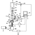
この第1実施の形態による装置は、図1に示すような構成に基づいて、概略的には、以下のような手順で近接場光学像を得る散乱モード近接場光学顕微鏡装置である。
【0048】
すなわち、レーザー光源2からの光は、試料1、プローブ100に入射し、このプローブ100の先端で散乱される。
【0049】
この散乱光は、対物レンズ3を通して、光検出器としての光電子増倍管(フォトマル)4で検出される。
【0050】
そして、このような散乱モード近接場光学顕微鏡装置では、試料1とプローブ100の先端との距離を一定に保ちつつ、圧電チューブスキャナー5で走査しながら上記散乱光を検出することによって、近接場光学像を得ることができる。
【0051】
(プローブ)
本実施形態による散乱モード近接場光学顕微鏡装置におけるプローブ100は、図2に示すようなカンチレバ一構造を有している。
【0052】
すなわち、このカンチレバ一における探針101の先端径は、レーザー光源2からの光の波長以下のサイズであり、この探針101先端は散乱体、あるいは発光体として機能する。
【0053】
そして、この探針101は、高屈折率誘電体又は金属、発光材料でできているか、あるいは、これらの材質でコーティングされていてもよい。
【0054】
いずれの場合でも、探針101は光の照射により光を散乱、あるいは吸収によりルミネッセンスを発光する。
【0055】
ここで、探針101は、照射する光の波長によって散乱効率あるいは発光効率が変化しさえすればよい。
【0056】
この探針101は、先端部半径が照射する光の波長以下であれば、先端から基部との接触面までの長さ、接触面でのサイズは照射する光の波長以上の構造でもよい。
【0057】
(加振)
上述のプローブ100は、図1に示されるように、探針加振手段である超音波振動子40を介してチップ保持具42により試料1の上方に支持されている。
【0058】
ここで、プローブ100は、光振幅変調手段でもある超音波振動子40とそれを駆動する高周波電源41とにより、高周波電源41の周波数ω1 で加振することも可能である。
【0059】
(位置センサー)
また、本実施形態の散乱モード近接場光学顕微鏡装置は、プローブ100の自由端の変位を検出する変位センサー6を有している。
【0060】
(粗動ステージ、試料)
また、本実施形態の散乱モード近接場光学顕微鏡装置では、試料1は試料テーブル10に載置され、この試料テーブル10は粗動ステージ45とともに、試料1と探針101先端との位置、距離についての粗い変調を実行する。
【0061】
ここで、粗動ステージ45は、粗動ステージ駆動回路46によって、コンピュータ11からの指令に基づいて駆動制御される。
【0062】
また、内部反射プリズム8は試料テーブル10と独立に懸架され、スライドグラス7とは光学的に結合している。
【0063】
なお、照射する光としてエバネッセント波を使うときには、内部反射プリズム8とスライドグラス7との結合にマッチングオイルが必要である。
【0064】
(精密な走査)
また、本実施形態の散乱モード近接場光学顕微鏡装置では、試料1の測定のための精密な走査は、次のようにしてなされる。
【0065】
図1において、圧電チューブスキャナー5は、制御回路9とコンピュータ11により制御されるスキャナー駆動回路13によって駆動され、試料テーブル10を三次元的に精密に移動させる。
【0066】
よって、試料テーブル10に載置されたスライドガラス7の上の試料1が、探針101に対して相対的に三次元的に移動されることになるので、探針101が試料1の表面を横切って精密に走査され、また、試料1の先端と探針101の表面の間の距離が微調整される。
【0067】
なお、本明細書においては、探針101が試料1表面を横切る走査をXY走査とも表現すると共に、探針101の先端と試料1表面との間の距離の調整をZ制御とも表現する。
【0068】
(光発生手段)
また、本実施形態の散乱モード近接場光学顕微鏡装置では、コヒーレント光を照射して探針101と試料1の間に光の場を発生させるための光発生手段を備えている。
【0069】
この光発生手段は、伝搬せずに局在する局在光を発生させる局在光発生手段と、伝搬する光を発生させる伝搬光発生手段とを有しており、試料の厚さや物性等諸特性により、そのいずれかを選択して動作させる。
【0070】
ここで、局在光は空間を伝搬しない光を意味し、例えば、エバネッセント光がこれにあたる。
【0071】
また、伝搬光は空間を伝搬する光を意味し、例えば、通常の伝搬光がこれにあたる。
【0072】
以下に、局在光発生手段と伝搬光発生手段について詳述する。
【0073】
まず、局在光発生手段、すなわち、ここでは、特に、エバネッセント光発生手段は、図1においてレーザー光源2、偏光や波長を制御する光学部品14、およびレーザの光路を制御するミラ−15,16、内部全反射プリズム17を有している。
【0074】
レーザー光源2から射出されたレーザー光は、各種光学部品14およびミラー15,16を通過して、内部全反射プリズム17に入射する。
【0075】
このときのレーザー光の入射角度は、内部全反射プリズム17の上面で全反射するように、ミラー16によって制御される。
【0076】
この結果、試料1の表面近傍にエバネッセント光が発生する。
【0077】
この場合、必要に応じてミラー16の後にレンズを挿入してレーザー光を収束させるようにしてもよい。
【0078】
また、伝搬光発生手段は、図1のレーザー光源2、光学部品14、二つのミラー15,16および図示しないミラーを有しており、上述したエバネッセント光発生手段における場合と同様にして得られた平行レーザビームを、ミラー15,16で反射させた後、図示しないミラーにより位置と角度を変更して、試料1の斜め上方から試料1と探針101の近傍に照射するように構成されている。
【0079】
(参照光入射手段)
さらに、本実施形態の散乱モード近接場光学顕微鏡装置では、対物レンズ3の上部に入射光(ω0 )とわずかに波長(δ)が異なる参照光を入射するためのビームスプリッタ30が配置されている。
【0080】
このビームスプリッタ30は、参照光と対物レンズ3とによって検出された信号が重なって干渉するように、参照光の光路を調整することができるような構成になっている。
【0081】
また、このビームスプリッタ30としては、参照光および信号光を効率よくフォトマル4に入射させるために、偏光ビームスプリッタを用いるようにしてもよい。
【0082】
ただし、このような偏光ビームスプリッタを用いる場合には、参照光と信号光との偏光を制御しなければならない。
【0083】
なお、参照光は、必要に応じて入射すればよい。
【0084】
(検出系)
また、本実施形態の散乱モード近接場光学顕微鏡装置では、図1に示すように、探針101先端近傍で発生した散乱光をプローブ100の上方に配置した対物レンズ3によつて集光し、必要に応じて偏光子19を通して散乱光検出鏡筒50内の光検出器である光電子増倍管(フォトマル)4で検出する。
【0085】
この散乱光検出鏡筒50は、レンズ群20、ピンホール21、光検出器である光電子増倍管(フォトマル)4を有している。
【0086】
ここで、ピンホール21は、対物レンズ3とレンズ群20に対して、探針101の先端と光学的に共役な位置に配置されている。
【0087】
すなわち、ピンホール21のある面は結像面になっている。
【0088】
これにより、探針101の先端近傍で発生された散乱光以外の成分をできるだけカットするようにしている。
【0089】
そして、光検出器である光電子増倍管(フォトマル)4は、受光した光強度に応じた電気信号を出力する。
【0090】
なお、ピンホール21の代わりに光ファイバーの単面がピンホール位置にあっても同様の効果が得られる。
【0091】
この場合、近接場信号は、光ファイバーを透過して光検出器である光電子増倍管(フォトマル)4で検出されるため、この光電子増倍管(フォトマル)4は散乱光検出鏡筒50上以外の任意の位置に設置することが可能になる。
【0092】
一般に、本実施形態のような散乱モード近接場光学顕微鏡装置では、近接場光学測定を行うために、探針101先端と試料1表面間の距離(ダイナミックモードでは平均距離)が、常に一定になるように制御されている。
【0093】
この状態で光入射手段により試料−探針先端付近に光の場を形成し、そこからの散乱光強度(または、その平均値)を光電子増倍管(フォトマル)4で検出し、PC等のコンピュータ11に内蔵される基板上のCPUで画像信号化および画像信号処理することにより、SNOM画像がモニター12上に得られる。
【0094】
(周波数(波長)変調手段)
また、一般に、本実施形態のような散乱モード近接場光学顕微鏡装置では、入射光の周波数(波長)は一定の周波数で変調がかかっている。
【0095】
周波数の変調の振幅すなわち変調による周波数(言い換えると波長の差)と変調の周期は測定対象試料に応じて選択する。
【0096】
この周波数(波長)変調手段として、ここでは、マルチライン発振のアルゴンレーザを用い、2種類の波長選択フィルターを図3に示すように組み合わせたチョッパーを用いて488nmと514nmの2波長を任意の周期で繰り返し照射できるようにしている。
【0097】
この場合、波長の繰り返し周波数は、入射光変調手段である図3に示すようなチョッパーの回転速度で決まり、機械的な回転を利用する場合には上限が数100kHzである。
【0098】
波長選択フィルターはレーザラインフィルターやバンドパスフィルター、ロングパスフィルターあるいは干渉フィルターを用いることができる。
【0099】
また、フィルター透過後のレーザ光強度が等しくなろようにNDフィルターを波長選択フィルターと組み合わせて強度の制御を行う必要がある。
【0100】
アルゴンレーザだけでなくマルチライン発振しているレーザ(例えば、ヘリカドレーザやYAGレーザ)やブロードバンド発振(例えば、色素レーザ)しているレーザでは上述の周波数変調手段(波長)を適用することができる。
【0101】
あるいは、波長可変レーザ(色素レーザやチタンサファイアレーザ)では、複屈折フィルターの回転やブリュースターガルボプレートの回転により周波数(波長)変調をかけることが可能である。
【0102】
前者の場合には、レーザ媒質のゲインの周波数帯域内(波長に換算して100nm程度)の幅で変調をかけることができ、後者の場合には1nm程度の周波数変調をかけることができる。
【0103】
この方法の場合、変調の周波数ω2 は10Hz程度である。
【0104】
シングルモード発振(エタロンつきアルゴンレーザや色素レーザ、チタンサファイアレーザ、安定化したヘリウムネオンレーザなど)をしているレーザでは、音響光学変調器により周波数変調をかけることが可能である。
【0105】
この場合、音響光学素子による変調の振幅(帯域)は1nm程度以下であるが、変調の周波数ω2 は、MHzのオーダーまで可能である。
【0106】
周波数(波長)変調手段は、使用したい波長と変調の振幅、周期によって選択しなければならない。
【0107】
(測定)
測定は入射光を探針101に照射し、探針101の先端で散乱された光を光検出器である光電子増倍管(フォトマル)4により検出し、その信号をコンピュータ11に取り込んで画像信号化した後、所定の画像信号処理を施すことによって行われる。
【0108】
この画像信号処理の結果は、コンピュータ11のモニター12に表示させることができる。
【0109】
いま、入射光の周波数(波長)が一定の周波数で変調されているとする。
【0110】
例えば、レーザの波長が600nmから570nmを一定の周波数で変動しているとする。
【0111】
この場合、探針101の先端が570nm付近にプラズモン共鳴波長をもっているとすれば、散乱光の強度は図4に示すような波長依存性を示すはずであり、入射光の波長がプラズモン共鳴周波数から外れると、散乱光強度は急激に減衰する。
【0112】
そこで、散乱光強度が最大になるような波長のときだけ散乱光を検出するように、散乱光強度信号を入射光の周波数変調に同期したロックインアンプ22に通して散乱光強度の振幅を画像化することができる。
【0113】
(探針振動)
プローブ100をそれに接続された超音波振動子40を用いて振動させることによって、探針101を、試料1の表面にほぼ垂直な方向に一定の振幅で振動させる。
【0114】
通常、探針100を上下方向に振動させると、散乱光強度は、探針101の振動周波数ω1 で変動する。
【0115】
この場合、散乱光強度は、入射光の波長変動によりω2 で変動していることから、検出された散乱信号のうち、差周波成分|ω2 −ω1 |もしくは和周波成分(ω2 +ω1 )をミキサー43を介してコンピュータ11によりロックイン検出することにより、不要散乱光を除去することができる。
【0116】
(ヘテロダイン検出)
本発明では、ビームスプリッタ30を介して入射される参照光は、散乱光に対して、光検出器である光電子増倍管(フォトマル)4の受光面において干渉するように調整されている。
【0117】
散乱光が入射光の周波数変調により変調がある場合、光電子増倍管(フォトマル)4で検出される干渉光のうち、差周波成分|ω2 −δ|もしくは和周波成分(ω2 +δ)をミキサー43を介してコンピュータ11によりロックイン検出することにより、探針以外の散乱源からの不要散乱光が強い場合でも探針からの散乱信号を抽出することができる。
【0118】
同様に、周波数変調のほかにプローブ100の振動がある場合には、さらにω1 との和周波、差周波成分を考慮した周波数成分をロックイン検出することにより、不要散乱光を効率よく除去することが可能になる。
【0119】
<第2実施の形態>
(探針のレーザトラップ)
本発明の第2実施の形態における装置構成は、後述するレーザトラップの構成を除いては、図1に示した装置構成と同様であるが、散乱探針101としては、レーザトラップされた金属微粒子が用いられるものとする。
【0120】
この金属微粒子としては、例えば、金や銀が良く用いられる。
【0121】
これらの金属微粒子は散乱光を増強するプラズモン共鳴を起こすことが知られており、プラズモン共鳴波長は微粒子の材質や直径に強く依存する。
【0122】
例えば、金の場合、図4に示すように直径に応じてプラズモン共鳴のピークが変化する。
【0123】
散乱探針が、金でその直径が80nmの場合、プラズモン共鳴のピーク波長は570nm付近である。
【0124】
(レーザトラップ)
レーザトラップされた金属微粒子をプローブ100として用いる場合、入射レーザ光源2のほかにトラップ用のレーザ光源が必要である。
【0125】
トラップ用のレーザ光の波長は、入射レーザ光源2からのレーザ光の波長と大きく異なっていた方が、トラップ用のレーザ光源によるノイズを除去し易い。
【0126】
図5の(a),(b)にレーザトラップの方法を示す。
【0127】
図5の(a)に示すトラップ用のレーザ光源60からのレーザ光は、図1に示している近接場測定用のレーザ光源2からのレーザ光と、それらの波長が互いに異なっている必要がある。
【0128】
トラップ用のレーザ光源60からのレーザ光は、コリメータレンズ61によって平行光線に整形された後、ビームスプリッタ63を介して散乱光集光用の対物レンズ3上方から試料面で収束するように導入される。
【0129】
試料ホルダー62上には、図5の(b)に示すように、試料1とそれを囲むような囲い64が設けられており、この囲い64の中には金コロイド水溶液あるいは銀コロイド水溶液65が満たされている。
【0130】
この囲い64の中の金コロイド水溶液あるいは銀コロイド水溶液65はカバーガラス66で蓋をして密封されている。
【0131】
対物レンズ3は、レーザトラップに用いる場合、N/Aの大きな対物レンズ3であることが好ましいために、油侵や水侵対物を用いてもよい。
【0132】
レーザトラップされた金属微粒子をプローブ100として用いる場合、金属微粒子は、トラップ用のレーザ光の収束点でトラップされる。
【0133】
トラップ位置が試料表面であれば、近接場測定用のレーザ光を照射して散乱光を対物レンズ3を介して上述したようにして検出する。
【0134】
このようにして検出された散乱光には、トラップ用のレーザ光が混入しているので、フィルター32などを使って、信号光成分と不要な光成分とを分離して検出する。
【0135】
なお、(測定)および(ヘテロダイン検出)に関しては、上述した第1実施の形態と同様に行うことが可能である。
【0136】
<第3実施の形態>
(探針)
本発明の第3実施の形態における装置構成は、図1に示した装置構成と同様であるが、探針101は、探針101の先端で散乱光がプラズモン共鳴を起こすものとしている。
【0137】
そのために、図2で示したようなプローブ100先端の探針101部分に金や銀がコーティングされたもの、あるいは図6の(a),(b)に示すようにプローブ100先端に金や銀のような金属微粒子101aあるいは突起101bがついたものを用いる。
【0138】
本実施の形態におけるその他の方法は、上述した第1実施の形態と同様にして実現することができる。
【0139】
<第4実施の形態>
(探針)
本発明の第4実施の形態における装置構成は、図1に示した装置構成と同様であるが、探針101は、探針101の先端でルミネッセンスを発生し、それが近接場光源として機能するものとしている。
【0140】
そのために、図2で示したようなプローブ100先端の探針101部分にルミネッセンスを発生させる物質、例えば、GaAs等の半導体や色素、色素をドープしたポリマー、希土類イオン等を分散した結晶やガラス、ポリマー等をコーティングもしくは先端に突起状にとりつける。
【0141】
(検出系)
上述の探針101の先端近傍で発生したルミネッセンスはプローブ100の上方に配置した対物レンズ3によつて集光し、図1では図示していないがルミネッセンス波長だけを選択的に透過させるフィルターを通して散乱光検出鏡筒50内の光検出器4で検出する。
【0142】
この光検出器4までの光学系は図1に示す通りである。
【0143】
また、光検出器4に入る前に、光検出器4の位置でファイバーに光を導入し、図示していないが分光器で光を分光し、ルミネセンス波長だけを光検出器で検出してもよい。
【0144】
(参照光)
本実施の形態における参照光の波長は、ルミネッセンス波長をω0 として、その+δもしくは−δに設定し、この参照光とルミネッセンス散乱光と光検出器4で干渉させる。
【0145】
本実施の形態におけるその他の方法は、上述した第1実施の形態と同様にして実現することができる。
【0146】
<第5実施の形態>
本発明の第5実施の形態における装置構成は、図1に示した装置構成と同様であるが、本実施の形態は入射レーザ光の波長変化に対して試料表面の特性が変化する場合の測定方法に関する。
【0147】
(実施例1)
本実施例では、測定試料としてたとえばルミネッセンスやラマン光を発生するような試料、あるいは表面でプラズモン共鳴が起きるような試料を扱うものとする。
【0148】
本実施例におけるその他の方法は、上述した第1実施の形態と同様にして実現することができる。
【0149】
(実施例2)
本実施例では、入射レーザ光の波長変化に対して試料表面で発生するルミネッセンスやラマン光強度あるいは波長が変化するような試料を扱うものとする。
【0150】
本実施例におけるその他の方法は、上述した第1実施の形態と同様にして実現することができる。
【0151】
(実施例3)
本実施例では、入射レーザ光の波長変化に対して試料表面でプラズモン共鳴が起きるような試料を扱うものとする。
【0152】
本実施例におけるその他の方法は、上述した第1実施の形態と同様にして実現することができる。
【0153】
そして、上述したような実施の形態で示した本明細書には、特許請求の範囲に示した請求項1乃至3以外にも、以下に付記1乃至付記12として示すような発明が含まれている。
【0154】
(付記1) 試料表面に光を入射する入射手段と、
先端が該試料に近接されて設置され、該先端で該入射光に由来する散乱光を発生させる探針と、
該散乱光を検出する光検出手段と、
を具備する近接場顕微鏡装置において、
該入射光の波長を第1の周波数で変調させる入射光変調手段と、
該探針を第2の周波数で振動させる探針加振手段と、
該散乱光と周波数δだけ異なる周波数の参照光を、該散乱光と平渉させる干渉手段と、
上記光検出手段の出力より、上記第1の周波数と上記周波数δのビート周波数成分を抽出する抽出手段と、
をさらに具備することを特徴とする近接場光学顕微鏡装置。
【0155】
(付記2) 試料表面に光を入射する入射手段と、
該入射光の波長以下のサイズの先端を持ち、該先端が該試料に近接して設置され、該入射光を該先端で散乱させる探針と、
該散乱光を検出する光検出手段と、
該探針または探針の支持部材の変位を検出する変位検出手段と、
該試料と探針を相対的に走査する走査手段と、
該変位検出手段からの信号をもとに探針と試料間の距離または探針圧を制御するための制御手段と、
該光検出手段からの信号の取り込んで画像化処理する手段とを有し、
該探針先端からの散乱光もしくは発生する光が入射光の波長によって変化するような近接場光学顕微鏡において、
該入射光の周波数(波長)を周期的に変調させる(変調周波数ω2 )ことによって発生する信号に周期的な変調を加え、散乱信号の変調周波数成分だけを抽出する信号検出手段を備えてなることを特徴とする走査型近接場光学顕微鏡。
【0156】
(付記3) 試料表面に光を入射する入射手段と、
該入射光の波長以下のサイズの先端を持ち、該先端が該試料に近接して設置され、該入射光を該先端で散乱させる探針と、
該散乱光を検出する光検出手段と、
該探針または探針の支持部材の変位を検出する変位検出手段と、
該試料と探針を相対的に走査する走査手段と、
該変位検出手段からの信号をもとに探針と試料間の距離または探針圧を制御するための制御手段と、
該光検出手段からの信号の取り込んで画像化処理する手段とを有し、
該探針先端からの散乱光もしくは発生する光が入射光の波長によって変化するような近接場光学顕微鏡において、
該入射光の周波数(波長)を周期的に変調させる(変調周波数ω2 )ことによって発生する信号に周期的な変調を加え、該探針を入射光の波長の変調周波数とわずかに異なる周波数(ω1 )で振動させ、散乱信号に入射光の波長変調および探針の振動による変調を同時に加えて、両者のビート周波数成分(|ω2 −ω1 |または(ω2 +ω1 ))だけを抽出する信号検出手段を備えてなることを特徴とする走査型近接場光学顕微鏡。
【0157】
(付記4) 試料表面に光を入射する入射手段と、
該入射光の波長以下のサイズの先端を持ち、該先端が該試料に近接して設置され、該入射光を該先端で散乱させる探針と、
該散乱光を検出する光検出手段と、
該探針または探針の支持部材の変位を検出する変位検出手段と、
該試料と探針を相対的に走査する走査手段と、
該変位検出手段からの信号をもとに探針と試料間の距離または探針圧を制御するための制御手段と、
該光検出手段からの信号の取り込んで画像化処理する手段とを有し、
該探針先端からの散乱光もしくは発生する光が入射光の波長によって変化するような近接場光学顕微鏡において、
該入射光の周波数(波長)を周期的に変調させる(変調周波数ω2 )ことによって周期的な変調を加え、
該散乱光の周波数(ω0 )とわずかに異なった周波数(ω0 +δ)を有する参照光と発生した信号とを干渉させて、両者のビート周波数成分(|ω2 −δ|または(ω2 +δ))だけを抽出する信号検出手段を備えてなることを特徴とする走査型近接場光学顕微鏡。
【0158】
(付記5) 試料表面に光を入射する入射手段と、
該入射光の波長以下のサイズの先端を持ち、該先端が該試料に近接して設置され、該入射光を該先端で散乱させる探針と、
該散乱光を検出する光検出手段と、
該探針または探針の支持部材の変位を検出する変位検出手段と、
該試料と探針を相対的に走査する走査手段と、
該変位検出手段からの信号をもとに探針と試料間の距離または探針圧を制御するための制御手段と、
該光検出手段からの信号の取り込んで画像化処理する手段とを有し、
該探針先端からの散乱光もしくは発生する光が入射光の波長によって変化するような近接場光学顕微鏡において、
該入射光の周波数(波長)を周期的に変調させる(変調周波数ω2 )ことによって発生する信号に周期的な変調を加え、該探針を入射光の波長の変調周波数とわずかに異なる周波数(ω1 )で振動させ、散乱信号に入射光の波長変調および探針の振動による変調を同時に加え、さらに散乱光の周波数(ω0 )とわずかに異なった周波数(ω0 +δ)を有する参照光と発生した信号とを干渉させて、参照光と信号のビート周波数成分だけを抽出する信号検出手段を備えてなることを特徴とする走査型近接場光学顕微鏡。
【0159】
(付記6) 該探針はレーザトラップされた金属微粒子であり、該探針は特定の波長を照射されるとプラズモン共鳴を起こすことを特徴とする付記2記載の走査型近接場光学顕微鏡。
【0160】
本発明の原理は上述した原理と同様であるが、レーザトラップされた金属微粒子では、特定の波長の光に対して散乱効率が増強する(プラズモン共鳴)特性をもつため、プラズモン共鳴ピーク付近でレーザの周波数(波長)を変調すると、効果は強く現れる。
【0161】
(付記7) 該探針はレーザトラップされた金属微粒子であり、該探針は特定の波長を照射されるとプラズモン共鳴を起こすことを特徴とする付記4記載の走査型近接場光学顕微鏡。
【0162】
(付記8) 該探針は特定の波長を照射されるとプラズモン共鳴を起こすことを特徴とする付記2記載の走査型近接場光学顕微鏡。
【0163】
本発明の原理は、上述した原理と同様であるが、本発明においてもプラズモン共鳴ピーク付近でレーザの周波数(波長)を変調すると、効果は強く現れる。
【0164】
(付記9) 該探針は特定の波長を照射されるとルミネッセンスを発生することを特徴とする付記2記載の走査型近接場光学顕微鏡。
【0165】
(付記10) 試料表面に光を入射する入射手段と、
該入射光の波長以下のサイズの先端を持ち、該先端が該試料に近接して設置され、該入射光を該先端で散乱させる探針と、
該散乱光を検出する光検出手段と、
該探針または探針の支持部材の変位を検出する変位検出手段と、
該試料と探針を相対的に走査する走査手段と、
該変位検出手段からの信号をもとに探針と試料間の距離または探針圧を制御するための制御手段と、
該光検出手段からの信号の取り込んで画像化処理する手段とを有し、
該試料表面の特性が該入射光の波長によって変化するような近接場光学顕微鏡において、
該入射光の周波数(波長)を周期的に変調させる(変調周波数ω2 )ことによって発生する信号に周期的な変調を加え、散乱信号の変調周波数成分だけを抽出する信号検出手段を備えてなることを特徴とする走査型近接場光学顕微鏡。
【0166】
本発明の原理は上述した原理と同様であるが、本発明においては入射光の波長の周期的な変調により、波長によって散乱光強度が変調するような散乱源からの不要散乱光の除去をより効率的に行うことが可能である。
【0167】
一方、探針の振動による不要散乱光の除去は波長によらず主に構造を伴った散乱源からの不要散乱光の除去を効率的に行うため、両者を組み合わせることで波長変化に対して散乱光強度が変化するような散乱源と波長に対して変化をともなわない散乱源からの両方の不要散乱光を効率よく除去することが可能であり、さらにこれに参照光を干渉させて検出することで不要散乱光が強い場合も両者の除去が可能になる。
【0168】
(付記11) 該試料表面の散乱体が特定の波長に対してプラズモン共鳴を起こすことを特徴とする付記10記載の走査型近接場光学顕微鏡。
【0169】
(付記12) 該試料表面のルミネッセンス発生が空間的に分布をもつことを特徴とする付記10記載の走査型近接場光学顕微鏡。
【0170】
【発明の効果】
従って、以上説明したように、本発明によれば、入射光の波長を変調することで試料からの信号に変調を加え、変調された信号からSNOM信号を抽出することでS/Nよい画像を得る信号検出手段を備えた近接場光学顕微鏡装置を提供することができる。
【図面の簡単な説明】
【図1】図1は、本発明の第1実施の形態による近接場光学顕微鏡装置の構成を示す図である。
【図2】図2は、本発明の第1実施形態による散乱モード近接場光学顕微鏡装置におけるプローブ100のカンチレバ一構造を示す図である。
【図3】図3は、本発明の第1実施形態による散乱モード近接場光学顕微鏡装置における周波数(波長)変調手段として、マルチライン発振のアルゴンレーザを用い、2種類の波長選択フィルターを組み合わせたチョッパー構造を示す図である。
【図4】図4は、本発明の第2実施形態による散乱モード近接場光学顕微鏡装置における散乱探針として用いられるレーザトラップされた金属微粒子が金の場合に、その直径に応じてプラズモン共鳴のピークが変化する様子を示す図である。
【図5】図5の(a),(b)は、本発明の第2実施形態による散乱モード近接場光学顕微鏡装置における散乱探針して用いられるレーザトラップの構造を示す図である。
【図6】図6の(a),(b)は、本発明の第3実施形態による散乱モード近接場光学顕微鏡装置に用いられるプローブ先端の探針構造を示す図である。
【符号の説明】
1…試料、
2…入射レーザ光源、
3…対物レンズ、
4…光検出器である光電子増倍管(フォトマル)、
5…圧電チューブスキャナ−、
6…変位センサー、
7…スライドグラス、
8…内部反射プリズム、
9…制御回路、
10…試料テーブル、
11…コンピュータ、
12…モニター、
13……スキャナー駆動回路、
14…光学部品、
15,16…ミラー、
17…内部全反射プリズム、
19…偏光子、
20…レンズ群、
21…ピンホール、
22…ロックインアンプ、
30…ビームスプリッタ、
32…フィルター、
50…散乱光検出鏡筒、
40…超音波振動子、
41…高周波電源、
43…ミキサー、
45…粗動ステージ、
46…粗動ステージ駆動回路、
60…トラップ用のレーザ光源、
61…コリメータレンズ、
62…試料ホルダー、
63…ビームスプリッタ、
64…囲い、
65…金コロイド水溶液あるいは銀コロイド水溶液、
66…カバーガラス、
100…プローブ、
101…探針、
101a…金属微粒子、
101b…突起。[0001]
BACKGROUND OF THE INVENTION
The present invention relates to a near-field optical microscope apparatus, and in particular, in a near-field optical microscope apparatus using a scattering probe, the S / N of a near-field signal when the signal intensity changes according to the change in incident light wavelength. The present invention relates to a near-field optical microscope apparatus provided with means for improving the above.
[0002]
[Prior art]
Recently, a scanning near-field optical microscope (SNOM) is an optical microscope having a resolution that exceeds the diffraction limit by detecting an evanescent wave. Development has been actively promoted for application to various characteristics of body optical waveguides, measurement of emission spectra of semiconductor quantum dots, evaluation of various characteristics of semiconductor surface light emitting devices, and the like.
[0003]
This SNOM is basically a device that detects a state of a light field (near field) in the vicinity of a sample by bringing a sharp probe close thereto while the sample is irradiated with light.
[0004]
U.S. Pat. No. 5,272,330, issued December 21, 1993 to Betzig et al., Introduces light into a probe whose tip is machined narrowly, thereby allowing evanescent to occur in the vicinity of the minute opening at the tip of the probe. SNOM which generates a field, makes this evanescent field contact with the sample, detects light generated by the contact between the evanescent field and the sample with a photodetector arranged under the sample, and performs two-dimensional mapping of transmitted light intensity Is disclosed.
[0005]
In this SNOM, a rod-like probe such as an optical fiber, a glass rod, or a quartz probe whose tip is processed to be thin is used.
[0006]
As an improved version of this probe, a rod-shaped probe having a portion other than the tip covered with a metal film is already on the market.
[0007]
An apparatus using such a probe has improved lateral resolution compared to an apparatus using a probe that is not coated with metal.
[0008]
N. F. van Hulst et al., Appl. Phys. Lett. 62 (5) P. 461 (1993) proposes a new SNOM that detects optical information of a sample while measuring the unevenness of the sample by AFM measurement using an AFM cantilever made of silicon nitride.
[0009]
The silicon AFM cantilever can obtain a high-resolution AFM image, and at the same time has a high refractive index, and therefore has a high light scattering efficiency, which is advantageous for a scattering SNOM probe.
[0010]
In this apparatus, the sample is placed on the internal total reflection prism, He—Ne laser light is irradiated onto the sample from the total reflection prism side, the sample is excited, and an evanescent light field is formed near the sample surface.
[0011]
Next, when a silicon nitride probe supported at the tip of the cantilever is inserted into the evanescent light field, the evanescent light that is a localized wave is converted into scattered light that is a propagating wave, and part of it is He− It propagates through a silicon nitride probe that is almost transparent to Ne laser light, and exits behind the cantilever.
[0012]
This light is collected by a lens disposed above the cantilever, and incident on the photomultiplier tube through a pinhole disposed at a position conjugate to the tip of the probe with respect to this lens. Outputs a SNOM signal.
[0013]
During the detection of the SNOM signal, the cantilever is measured by the optical displacement detection sensor in the same manner as in the normal AFM measurement. For example, the cantilever is piezoelectric so as to keep the displacement at a predetermined constant value. The scanner is feedback controlled.
[0014]
Therefore, during one scan, SNOM measurement is performed based on the scanning signal and the SNOM signal, and AFM measurement is performed based on the scanning signal and the feedback control signal.
[0015]
Further, a new SNOM (scattering mode SNOM) has been proposed that utilizes the fact that a high-refractive-index dielectric or metal having a subwavelength structure strongly scatters near-field terms.
[0016]
Fischer et al. (Phys. Rev. Lett. 62 (1989) p. 458) is a method in which a metal sphere is formed by injecting a laser with a plasmon excitation frequency from above on a sample obtained by attaching a fine metal sphere to a transparent plane. Local plasmons are generated in the image and used as scattered light to produce an image.
[0017]
Scattering efficiency from the tip of the probe strongly depends on the wavelength of the light and the material and size of the scatterer. The light scattered by the probe caused plasmon resonance depending on the material and size of the scatterer and the wavelength of the incident light. In this case, it is known that the scattering efficiency is improved.
[0018]
For example, in the case of gold, it is assumed that the gold particle is a scatterer approximated by a point, and when light is irradiated and the scattering efficiency when the wavelength is changed is examined, the wavelength of the light is around 550 nm. It has a scattering efficiency peak with a width of several tens of nm.
[0019]
If light having a wavelength in the vicinity of this peak is used as incident light, the scattering efficiency is increased. Therefore, it is possible to obtain a higher S / N than when using light of other wavelengths.
[0020]
[Problems to be solved by the invention]
As described above, various types of SNOM devices have been disclosed. However, if there is a strong scattering source other than the probe, the scattered light from the source is picked up and the S / N of the image is deteriorated. Yes.
[0021]
In order to solve this, various ideas for improving S / N in signal detection of a near-field microscope have been proposed.
[0022]
In order to overcome this, the following method is often used.
[0023]
That is, when the probe is vibrated longitudinally in the vicinity of the sample surface, multiple scattering between the probe and the sample occurs only when the probe approaches the sample, and the signal at this time vibrates with time.
[0024]
On the other hand, the scattered light from the scattering source is constant in time.
[0025]
Therefore, out of the signal received by the photodetector, the signal intensity amplitude synchronized with the probe frequency is taken out by the lock-in amplifier, and the signal from the probe alone is obtained by subtracting the light intensity from the scattering source. It can be obtained.
[0026]
Furthermore, Sasaki discloses an idea of applying heterodyne in combination with the above method to detect a near-field microscope signal in Japanese Patent Application Laid-Open No. 10-170522.
[0027]
The present invention has been made in view of the above circumstances, and modulates the signal from the sample by modulating the wavelength of the incident light, and extracts the SNOM signal from the modulated signal, thereby improving the S / N image. An object of the present invention is to provide a near-field optical microscope apparatus provided with a signal detection means for obtaining the above.
[0028]
[Means for Solving the Problems]
According to the present invention, in order to solve the above problems,
(1) an incident means for making light incident on the sample surface;
A probe having a tip placed close to the sample and generating scattered light derived from the incident light at the tip;
Light detection means for detecting the scattered light;
In a near-field optical microscope apparatus comprising:
The wavelength of the incident lightFirstIncident light modulating means for modulating the frequency;
Probe excitation means for vibrating the probe at a second frequency;
From the output of the light detection means, the aboveThe beat frequency component of the first frequency and the second frequencyExtracting means for extracting;
The near-field optical microscope apparatus is further provided.
[0029]
Further, according to the present invention, in order to solve the above problems,
(2) an incident means for making light incident on the sample surface;
A tip that is placed close to the sample and generates scattered light derived from the incident light at the tip;
Light detection means for detecting the scattered light;
In a near-field optical microscope apparatus comprising:
Incident light modulation means for modulating the wavelength of the incident light at a first frequency;
Interference means for causing the reference light having a frequency different from the scattered light by a frequency δ to interfere with the scattered light;
From the output of the light detection means, the first frequency andOf the above frequency δExtraction means for extracting beat frequency components;
The near-field optical microscope apparatus is further provided.
[0030]
Further, according to the present invention, in order to solve the above problems,
(3) an incident means for making light incident on the sample surface;
A tip that is placed close to the sample and generates scattered light derived from the incident light at the tip;
Light detection means for detecting the scattered light;
In a near-field microscope apparatus comprising:
Incident light modulation means for modulating the wavelength of the incident light at a first frequency;
Probe excitation means for vibrating the probe at a second frequency;
Interference means for interfering with the scattered light with a reference light having a frequency different from the scattered light by a frequency δ;
Extraction means for extracting beat frequency components of the first frequency and the frequency δ from the output of the light detection means;
The near-field optical microscope apparatus is further provided.
Further, according to the present invention, in order to solve the above problems,
(4) an incident means for making light incident on the sample surface;
A probe having a tip having a size equal to or smaller than the wavelength of the incident light, the tip is disposed in proximity to the sample, and the probe scatters the incident light at the tip;
Light detection means for detecting the scattered light;
A displacement detecting means for detecting the displacement of the probe or the support member of the probe;
Scanning means for relatively scanning the sample and the probe;
Control means for controlling the distance between the probe and the sample or the probe pressure based on the signal from the displacement detection means, and means for capturing and imaging the signal from the light detection means In the near-field optical microscope in which the scattered light from the probe tip or generated light changes depending on the wavelength of the incident light,
A near-field comprising signal detection means for periodically modulating a signal generated by periodically modulating the frequency or wavelength of the incident light and extracting only the modulation frequency component of the scattered signal. An optical microscope is provided.
Further, according to the present invention, in order to solve the above problems,
(5) an incident means for making light incident on the sample surface;
A probe having a tip having a size equal to or smaller than the wavelength of the incident light, the tip is disposed in proximity to the sample, and the probe scatters the incident light at the tip;
Light detection means for detecting the scattered light;
A displacement detecting means for detecting the displacement of the probe or the support member of the probe;
Scanning means for relatively scanning the sample and the probe;
Control means for controlling the distance between the probe and the sample or the probe pressure based on the signal from the displacement detection means;
Means for capturing a signal from the light detection means and performing image processing,
In the near-field optical microscope in which the scattered light from the probe tip or generated light changes depending on the wavelength of the incident light,
A periodic modulation is applied to a signal generated by periodically modulating the frequency or wavelength of the incident light with a predetermined modulation frequency (ω 2), and the probe has a frequency (ω 1 different from the modulation frequency of the wavelength of the incident light). ), And the signal detection means for extracting only the beat frequency component (| ω2 −ω1 | or (ω2 + ω1)) of the scattered signal by simultaneously adding the wavelength modulation of the incident light and the modulation by the probe vibration to the scattered signal. A near-field optical microscope is provided.
Further, according to the present invention, in order to solve the above problems,
(6) an incident means for making light incident on the sample surface;
A probe having a tip having a size equal to or smaller than the wavelength of the incident light, the tip is disposed in proximity to the sample, and the probe scatters the incident light at the tip;
Light detection means for detecting the scattered light;
A displacement detecting means for detecting the displacement of the probe or the support member of the probe;
Scanning means for relatively scanning the sample and the probe;
Control means for controlling the distance between the probe and the sample or the probe pressure based on the signal from the displacement detection means;
Means for capturing a signal from the light detection means and performing image processing,
In the near-field optical microscope in which the scattered light from the probe tip or generated light changes depending on the wavelength of the incident light,
Reference light having a frequency (ω0 + δ) different from the frequency (ω0) of the scattered light by periodically modulating the frequency or wavelength of the incident light with a predetermined modulation frequency (ω2). And a generated signal are provided, and a near-field optical microscope is provided that includes signal detection means for extracting only the beat frequency component (| ω 2 −δ | or (ω 2 + δ)) of both. The
Further, according to the present invention, in order to solve the above problems,
(7) an incident means for making light incident on the sample surface;
A probe having a tip having a size equal to or smaller than the wavelength of the incident light, the tip is disposed in proximity to the sample, and the probe scatters the incident light at the tip;
Light detection means for detecting the scattered light;
A displacement detecting means for detecting the displacement of the probe or the support member of the probe;
Scanning means for relatively scanning the sample and the probe;
Control means for controlling the distance between the probe and the sample or the probe pressure based on the signal from the displacement detection means;
Means for capturing a signal from the light detection means and performing image processing,
In the near-field optical microscope in which the scattered light from the probe tip or generated light changes depending on the wavelength of the incident light,
A periodic modulation is applied to a signal generated by periodically modulating the frequency or wavelength of the incident light with a predetermined modulation frequency (ω 2), and the probe has a frequency (ω 1 different from the modulation frequency of the wavelength of the incident light). ), The wavelength modulation of the incident light and the modulation due to the probe vibration are simultaneously added to the scattered signal, and the reference light having a frequency (ω0 + δ) different from the scattered light frequency (ω0) and the generated signal are There is provided a near-field optical microscope characterized by comprising signal detection means for extracting only the reference light and the beat frequency component (| ω 2 −δ |) of the signal by interference.
Further, according to the present invention, in order to solve the above problems,
(8) The near-field optical microscope according to any one of (4) to (7), wherein the probe causes plasmon resonance when irradiated with a specific wavelength.
Further, according to the present invention, in order to solve the above problems,
(9) The near-field optical microscope according to (8) is provided, wherein the probe is a metal particle trapped with a laser.
Further, according to the present invention, in order to solve the above problems,
(10) The near-field optical microscope according to any one of (4) to (7), wherein the probe generates luminescence when irradiated with a specific wavelength.
Further, according to the present invention, in order to solve the above problems,
(11) an incident means for making light incident on the sample surface;
A probe having a tip having a size equal to or smaller than the wavelength of the incident light, the tip is disposed in proximity to the sample, and the probe scatters the incident light at the tip;
Light detection means for detecting the scattered light;
A displacement detecting means for detecting the displacement of the probe or the support member of the probe;
Scanning means for relatively scanning the sample and the probe;
Control means for controlling the distance between the probe and the sample or the probe pressure based on the signal from the displacement detection means;
Means for capturing a signal from the light detection means and performing image processing,
In a near-field optical microscope in which the characteristics of the sample surface change depending on the wavelength of the incident light,
A near-field comprising signal detection means for periodically modulating a signal generated by periodically modulating the frequency or wavelength of the incident light and extracting only the modulation frequency component of the scattered signal. An optical microscope is provided.
Further, according to the present invention, in order to solve the above problems,
(12) The near-field optical microscope according to (11), wherein the scatterer on the sample surface causes plasmon resonance with respect to a specific wavelength.
Further, according to the present invention, in order to solve the above problems,
(13) The luminescence generation on the sample surface has a spatial distribution. (11) A near-field optical microscope according to (11) is provided.
[0031]
DETAILED DESCRIPTION OF THE INVENTION
First, the outline and principle of signal detection means employed in the near-field optical microscope apparatus of the present invention will be described.
[0032]
That is, the signal detection means employed in the near-field optical microscope apparatus of the present invention has an incident means for making light incident on the sample surface and a tip having a size not larger than the wavelength of the incident light, and the tip is close to the sample. A probe that scatters the incident light at the tip, a light detection means that detects scattered light, a displacement detection means that detects the displacement of the probe or a support member of the probe, a sample and a probe Scanning means for relatively scanning the needle, control means for controlling the distance between the probe and the sample or the probe pressure based on the signal from the displacement detection means, and the signal from the light detection means A near-field optical microscope in which scattered light from the tip of the probe or generated light varies depending on the wavelength of incident light.
The frequency (wavelength) of the incident light is periodically modulated (modulation frequency ω2) Is periodically modulated to extract only the modulation frequency component of the scattered signal.
[0033]
Further, the signal detection means employed in the near-field optical microscope apparatus of the present invention is a near-field optical microscope as described above.
The frequency (wavelength) of the incident light is periodically modulated (modulation frequency ω2) To periodically modulate the signal generated by the probe, and the probe has a frequency slightly different from the modulation frequency of the wavelength of the incident light (ω1), And simultaneously adding the wavelength modulation of the incident light and the modulation by the probe vibration to the scattered signal, and the beat frequency component (| ω2−ω1| Or (ω2+ Ω1)) Only.
[0034]
Further, the signal detection means employed in the near-field optical microscope apparatus of the present invention is a near-field optical microscope as described above.
The frequency (wavelength) of the incident light is periodically modulated (modulation frequency ω2) To add periodic modulation,
The frequency of the scattered light (ω0) And slightly different frequency (ω0+ Δ) is caused to interfere with the generated signal and the beat frequency component (| ω2−δ | or (ω2Only + δ)) is extracted.
[0035]
And the principle of the signal detection by the signal detection means of such a configuration is as follows.
[0036]
That is, assuming that the scattered light Ep from the probe on the sample is modulated so that the incident light varies with a sine function at the frequency ω2,
Ep= Ep0+ Ep1sinω2t + Ep2sin2ω2+ ...
It can be expressed as
[0037]
However, this is a case where the scattering efficiency is periodically modulated in proportion to the frequency of the incident laser light.
[0038]
The detection light I when there is a scattering source other than the probe is
I = | Es+ Ep0+ Ep1sinω2t |2
And Es<< EpWhen EsCan be ignored, Ep0× Ep1Can be extracted by the lock-in
[0039]
Furthermore, the probe is ω2Slightly different frequency ω1Heterodyne detection ((ω2± ω1For example, unnecessary scattered light that cannot be removed only by frequency modulation can be efficiently removed.
[0040]
This is because the incident light has a frequency ω2This is effective when the sample fluctuates in binary or when the sample generates luminescence depending on the wavelength of incident light.
[0041]
For example, in the former, since the wavelength of incident light repeats two wavelengths at a constant time, the peak of scattered light intensity as described later does not appear clearly.
[0042]
In such a case, unnecessary scattered light can be more effectively removed by vibrating the probe.
[0043]
In addition, the signal from the scattering source is larger than the scattering signal from the probe (Es>> Ep) If EsCan not be ignored.
[0044]
Scattered light frequency (ω0) To δ by reference light having a different frequency (wavelength) as reference light and interfering with scattered light from the probe on the detector to detect heterodyne ((ω2If the ± δ) component is extracted, this can be removed even if unnecessary scattered light from the scattering source is strong.
[0045]
Further, the probe is vibrated while applying frequency modulation, and the resulting scattered light and the reference light are made to interfere with each other, whereby the signal from the scattering source is larger than the scattered signal from the probe (Es>> Ep) Even in such a case, it is possible to efficiently remove unnecessary scattered light from both a scattering source whose scattered light intensity changes with wavelength change and a scattering source which does not change with wavelength. .
[0046]
Next, an embodiment of the near-field optical microscope apparatus of the present invention provided with signal detection means based on the above outline and principle will be described with reference to the drawings.
[0047]
<First embodiment>
(Device configuration)
The apparatus according to the first embodiment is roughly a scattering mode near-field optical microscope apparatus that obtains a near-field optical image in the following procedure based on the configuration shown in FIG.
[0048]
That is, the light from the laser light source 2 enters the sample 1 and the
[0049]
The scattered light is detected by a photomultiplier tube (photomultiplier) 4 as a photodetector through the
[0050]
In such a scattering mode near-field optical microscope apparatus, the scattered light is detected while scanning with the
[0051]
(probe)
The
[0052]
That is, the tip diameter of the
[0053]
The
[0054]
In any case, the
[0055]
Here, the
[0056]
The
[0057]
(Excitation)
As shown in FIG. 1, the
[0058]
Here, the
[0059]
(Position sensor)
Further, the scattering mode near-field optical microscope apparatus of the present embodiment has a displacement sensor 6 that detects the displacement of the free end of the
[0060]
(Coarse movement stage, sample)
Further, in the scattering mode near-field optical microscope apparatus of the present embodiment, the sample 1 is placed on the sample table 10, and the sample table 10, together with the
[0061]
Here, the
[0062]
The
[0063]
Note that, when an evanescent wave is used as the irradiation light, matching oil is required for coupling the
[0064]
(Precise scanning)
Further, in the scattering mode near-field optical microscope apparatus of the present embodiment, precise scanning for measuring the sample 1 is performed as follows.
[0065]
In FIG. 1, the
[0066]
Therefore, the sample 1 on the slide glass 7 placed on the sample table 10 is moved three-dimensionally relative to the
[0067]
In the present specification, scanning in which the
[0068]
(Light generation means)
In addition, the scattering mode near-field optical microscope apparatus of the present embodiment includes light generating means for irradiating coherent light to generate a light field between the
[0069]
This light generating means has a localized light generating means for generating localized light that does not propagate, and a propagating light generating means for generating propagating light. Depending on the characteristics, one of them is selected and operated.
[0070]
Here, the localized light means light that does not propagate in space, for example, evanescent light.
[0071]
Propagating light means light propagating in space, for example, normal propagating light.
[0072]
Hereinafter, the localized light generation means and the propagation light generation means will be described in detail.
[0073]
First, the localized light generation means, that is, here, in particular, the evanescent light generation means is the laser light source 2 in FIG. 1, the optical component 14 for controlling the polarization and wavelength, and the
[0074]
The laser light emitted from the laser light source 2 passes through the various optical components 14 and the
[0075]
The incident angle of the laser beam at this time is controlled by the
[0076]
As a result, evanescent light is generated near the surface of the sample 1.
[0077]
In this case, if necessary, a lens may be inserted after the
[0078]
Further, the propagation light generation means has the laser light source 2 of FIG. 1, the optical component 14, the two
[0079]
(Reference light incident means)
Furthermore, in the scattering mode near-field optical microscope apparatus of the present embodiment, incident light (ω0) And a
[0080]
The
[0081]
Further, as the
[0082]
However, when such a polarization beam splitter is used, the polarization of the reference light and the signal light must be controlled.
[0083]
Note that the reference light may be incident as necessary.
[0084]
(Detection system)
Further, in the scattering mode near-field optical microscope apparatus of the present embodiment, as shown in FIG. 1, the scattered light generated near the tip of the
[0085]
The scattered
[0086]
Here, the
[0087]
That is, the surface with the
[0088]
Thereby, components other than scattered light generated near the tip of the
[0089]
A photomultiplier tube (photomultiplier) 4 serving as a photodetector outputs an electrical signal corresponding to the received light intensity.
[0090]
The same effect can be obtained even if a single surface of the optical fiber is located at the pinhole position instead of the
[0091]
In this case, since the near-field signal passes through the optical fiber and is detected by the photomultiplier tube (photomultiplier) 4 that is a photodetector, the photomultiplier tube (photomultiplier) 4 is used for the scattered
[0092]
In general, in the scattering mode near-field optical microscope apparatus as in the present embodiment, the distance between the tip of the
[0093]
In this state, a light field is formed in the vicinity of the tip of the sample-probe by the light incident means, and the scattered light intensity (or its average value) is detected by the photomultiplier tube (photomultiplier) 4 and then PC or the like The SNOM image is obtained on the
[0094]
(Frequency (wavelength) modulation means)
In general, in the scattering mode near-field optical microscope apparatus as in this embodiment, the frequency (wavelength) of incident light is modulated at a constant frequency.
[0095]
The amplitude of the frequency modulation, that is, the frequency by the modulation (in other words, the wavelength difference) and the modulation period are selected according to the sample to be measured.
[0096]
As this frequency (wavelength) modulation means, here, a multi-line oscillation argon laser is used, and two wavelengths of 488 nm and 514 nm are arbitrarily cycled using a chopper in which two types of wavelength selection filters are combined as shown in FIG. Can be repeatedly irradiated.
[0097]
In this case, the repetition frequency of the wavelength is determined by the rotation speed of the chopper as shown in FIG. 3 which is the incident light modulation means, and the upper limit is several hundred kHz when mechanical rotation is used.
[0098]
As the wavelength selection filter, a laser line filter, a band pass filter, a long pass filter or an interference filter can be used.
[0099]
Further, it is necessary to control the intensity by combining the ND filter with the wavelength selection filter so that the laser light intensity after passing through the filter becomes equal.
[0100]
The above-described frequency modulation means (wavelength) can be applied not only to an argon laser but also to a laser that performs multiline oscillation (for example, a helicad laser or YAG laser) or a laser that performs broadband oscillation (for example, a dye laser).
[0101]
Alternatively, in a wavelength tunable laser (dye laser or titanium sapphire laser), frequency (wavelength) modulation can be performed by rotating a birefringent filter or a Brewster galvo plate.
[0102]
In the former case, modulation can be applied within the frequency band of the gain of the laser medium (converted to a wavelength of about 100 nm), and in the latter case, frequency modulation of about 1 nm can be applied.
[0103]
For this method, the modulation frequency ω2Is about 10 Hz.
[0104]
In a laser having a single mode oscillation (such as an argon laser with an etalon, a dye laser, a titanium sapphire laser, or a stabilized helium neon laser), it can be frequency-modulated by an acousto-optic modulator.
[0105]
In this case, the amplitude (band) of modulation by the acoustooptic device is about 1 nm or less, but the modulation frequency ω2Is possible up to the order of MHz.
[0106]
The frequency (wavelength) modulation means must be selected according to the wavelength to be used, the amplitude and period of the modulation.
[0107]
(Measurement)
The measurement is performed by irradiating the
[0108]
The result of this image signal processing can be displayed on the
[0109]
Assume that the frequency (wavelength) of incident light is modulated at a constant frequency.
[0110]
For example, it is assumed that the laser wavelength varies from 600 nm to 570 nm at a constant frequency.
[0111]
In this case, if the tip of the
[0112]
Therefore, the scattered light intensity signal is passed through the lock-in
[0113]
(Probe vibration)
The
[0114]
Normally, when the
[0115]
In this case, the scattered light intensity depends on the wavelength variation of the incident light.2Of the detected scattered signal, the difference frequency component | ω2−ω1| Or the sum frequency component (ω2+ Ω1) Is detected by the computer 11 via the
[0116]
(Heterodyne detection)
In the present invention, the reference light incident through the
[0117]
When the scattered light is modulated by the frequency modulation of the incident light, the difference frequency component | ω out of the interference light detected by the photomultiplier tube (photomultiplier) 42−δ | or the sum frequency component (ω2+ Δ) is detected by the computer 11 via the
[0118]
Similarly, if there is vibration of the
[0119]
<Second Embodiment>
(Laser trap of probe)
The apparatus configuration in the second embodiment of the present invention is the same as the apparatus configuration shown in FIG. 1 except for the laser trap configuration described later. However, as the
[0120]
For example, gold or silver is often used as the metal fine particles.
[0121]
These metal fine particles are known to cause plasmon resonance that enhances scattered light, and the plasmon resonance wavelength strongly depends on the material and diameter of the fine particles.
[0122]
For example, in the case of gold, the peak of plasmon resonance changes depending on the diameter as shown in FIG.
[0123]
When the scattering probe is gold and its diameter is 80 nm, the peak wavelength of plasmon resonance is around 570 nm.
[0124]
(Laser trap)
When laser trapped metal fine particles are used as the
[0125]
If the wavelength of the laser beam for trapping is significantly different from the wavelength of the laser beam from the incident laser light source 2, it is easier to remove noise from the laser light source for trapping.
[0126]
5A and 5B show a laser trap method.
[0127]
The laser light from the trapping
[0128]
Laser light from the trapping
[0129]
On the
[0130]
The colloidal gold aqueous solution or the silver colloidal
[0131]
Since the
[0132]
When laser trapped metal particles are used as the
[0133]
If the trap position is the sample surface, the laser light for near-field measurement is irradiated and the scattered light is detected through the
[0134]
Since the trapped laser light is mixed in the scattered light detected in this manner, the signal light component and the unnecessary light component are separated and detected using the
[0135]
Note that (measurement) and (heterodyne detection) can be performed in the same manner as in the first embodiment described above.
[0136]
<Third Embodiment>
(Probe)
The apparatus configuration in the third embodiment of the present invention is the same as the apparatus configuration shown in FIG. 1, but the
[0137]
Therefore, the
[0138]
Other methods in the present embodiment can be realized in the same manner as in the first embodiment described above.
[0139]
<Fourth embodiment>
(Probe)
The apparatus configuration in the fourth embodiment of the present invention is the same as the apparatus configuration shown in FIG. 1, but the
[0140]
For this purpose, a substance that generates luminescence in the
[0141]
(Detection system)
The luminescence generated in the vicinity of the tip of the
[0142]
The optical system up to the photodetector 4 is as shown in FIG.
[0143]
Further, before entering the photodetector 4, light is introduced into the fiber at the position of the photodetector 4, and although not shown, the light is dispersed by the spectrometer and only the luminescence wavelength is detected by the photodetector. Also good.
[0144]
(Reference light)
In this embodiment, the wavelength of the reference light is the luminescence wavelength ω0Is set to + δ or −δ, and the reference light, the luminescence scattered light, and the photodetector 4 are caused to interfere with each other.
[0145]
Other methods in the present embodiment can be realized in the same manner as in the first embodiment described above.
[0146]
<Fifth embodiment>
The apparatus configuration in the fifth embodiment of the present invention is the same as the apparatus configuration shown in FIG. 1, but the present embodiment is a measurement when the characteristics of the sample surface change with respect to the wavelength change of the incident laser beam. Regarding the method.
[0147]
Example 1
In this embodiment, for example, a sample that generates luminescence or Raman light, or a sample that causes plasmon resonance on the surface is handled as a measurement sample.
[0148]
Other methods in the present embodiment can be realized in the same manner as in the first embodiment described above.
[0149]
(Example 2)
In this embodiment, it is assumed that a sample whose luminescence, Raman light intensity or wavelength generated on the sample surface changes with respect to the wavelength change of the incident laser beam is handled.
[0150]
Other methods in the present embodiment can be realized in the same manner as in the first embodiment described above.
[0151]
(Example 3)
In this embodiment, it is assumed that a sample in which plasmon resonance occurs on the sample surface with respect to a change in wavelength of incident laser light is handled.
[0152]
Other methods in the present embodiment can be realized in the same manner as in the first embodiment described above.
[0153]
In addition, the present specification shown in the embodiment as described above includes inventions as shown in the following supplementary notes 1 to 12 in addition to the claims 1 to 3 shown in the claims. Yes.
[0154]
(Appendix 1) Incident means for making light incident on the sample surface;
A tip that is placed close to the sample and generates scattered light derived from the incident light at the tip;
Light detection means for detecting the scattered light;
In a near-field microscope apparatus comprising:
Incident light modulation means for modulating the wavelength of the incident light at a first frequency;
Probe excitation means for vibrating the probe at a second frequency;
Interference means for interfering with the scattered light with a reference light having a frequency different from the scattered light by a frequency δ;
Extraction means for extracting beat frequency components of the first frequency and the frequency δ from the output of the light detection means;
The near-field optical microscope apparatus further comprising:
[0155]
(Appendix 2) Incident means for making light incident on the sample surface;
A probe having a tip having a size equal to or smaller than the wavelength of the incident light, the tip is disposed in proximity to the sample, and the probe scatters the incident light at the tip;
Light detection means for detecting the scattered light;
A displacement detecting means for detecting the displacement of the probe or the support member of the probe;
Scanning means for relatively scanning the sample and the probe;
Control means for controlling the distance between the probe and the sample or the probe pressure based on the signal from the displacement detection means;
Means for capturing a signal from the light detection means and performing image processing,
In the near-field optical microscope in which the scattered light from the probe tip or generated light changes depending on the wavelength of the incident light,
The frequency (wavelength) of the incident light is periodically modulated (modulation frequency ω2The scanning near-field optical microscope is characterized by comprising signal detection means for applying periodic modulation to the signal generated by the above and extracting only the modulation frequency component of the scattered signal.
[0156]
(Additional remark 3) The incident means which injects light into the sample surface,
A probe having a tip having a size equal to or smaller than the wavelength of the incident light, the tip is disposed in proximity to the sample, and the probe scatters the incident light at the tip;
Light detection means for detecting the scattered light;
A displacement detecting means for detecting the displacement of the probe or the support member of the probe;
Scanning means for relatively scanning the sample and the probe;
Control means for controlling the distance between the probe and the sample or the probe pressure based on the signal from the displacement detection means;
Means for capturing a signal from the light detection means and performing image processing,
In the near-field optical microscope in which the scattered light from the probe tip or generated light changes depending on the wavelength of the incident light,
The frequency (wavelength) of the incident light is periodically modulated (modulation frequency ω2) To periodically modulate the signal generated by the probe, and the probe has a frequency slightly different from the modulation frequency of the wavelength of the incident light (ω1), And simultaneously adding the wavelength modulation of the incident light and the modulation by the probe vibration to the scattered signal, and the beat frequency component (| ω2−ω1| Or (ω2+ Ω1A scanning near-field optical microscope characterized by comprising signal detection means for extracting only ()).
[0157]
(Supplementary Note 4) Incident means for making light incident on the sample surface;
A probe having a tip having a size equal to or smaller than the wavelength of the incident light, the tip is disposed in proximity to the sample, and the probe scatters the incident light at the tip;
Light detection means for detecting the scattered light;
A displacement detecting means for detecting the displacement of the probe or the support member of the probe;
Scanning means for relatively scanning the sample and the probe;
Control means for controlling the distance between the probe and the sample or the probe pressure based on the signal from the displacement detection means;
Means for capturing a signal from the light detection means and performing image processing,
In the near-field optical microscope in which the scattered light from the probe tip or generated light changes depending on the wavelength of the incident light,
The frequency (wavelength) of the incident light is periodically modulated (modulation frequency ω2) To add periodic modulation,
The frequency of the scattered light (ω0) And slightly different frequency (ω0+ Δ) is caused to interfere with the generated signal and the beat frequency component (| ω2−δ | or (ω2A scanning near-field optical microscope comprising signal detection means for extracting only + δ)).
[0158]
(Additional remark 5) The incident means which injects light into the sample surface,
A probe having a tip having a size equal to or smaller than the wavelength of the incident light, the tip is disposed in proximity to the sample, and the probe scatters the incident light at the tip;
Light detection means for detecting the scattered light;
A displacement detecting means for detecting the displacement of the probe or the support member of the probe;
Scanning means for relatively scanning the sample and the probe;
Control means for controlling the distance between the probe and the sample or the probe pressure based on the signal from the displacement detection means;
Means for capturing a signal from the light detection means and performing image processing,
In the near-field optical microscope in which the scattered light from the probe tip or generated light changes depending on the wavelength of the incident light,
The frequency (wavelength) of the incident light is periodically modulated (modulation frequency ω2) To periodically modulate the signal generated by the probe, and the probe has a frequency slightly different from the modulation frequency of the wavelength of the incident light (ω1), And simultaneously add the wavelength modulation of the incident light and the modulation by the probe vibration to the scattered signal.0) And slightly different frequency (ω0A scanning near-field optical microscope comprising signal detecting means for extracting only the reference light and the beat frequency component of the signal by causing the reference light having + δ) to interfere with the generated signal.
[0159]
(Supplementary note 6) The scanning near-field optical microscope according to Supplementary note 2, wherein the probe is a laser trapped metal fine particle, and the probe causes plasmon resonance when irradiated with a specific wavelength.
[0160]
The principle of the present invention is the same as that described above. However, the laser trapped metal fine particles have the characteristic that the scattering efficiency is enhanced (plasmon resonance) with respect to light of a specific wavelength, so that the laser is near the plasmon resonance peak. If the frequency (wavelength) is modulated, the effect appears strongly.
[0161]
(Supplementary note 7) The scanning near-field optical microscope according to supplementary note 4, wherein the probe is a metal particle trapped with a laser, and the probe causes plasmon resonance when irradiated with a specific wavelength.
[0162]
(Supplementary note 8) The scanning near-field optical microscope according to supplementary note 2, wherein the probe causes plasmon resonance when irradiated with a specific wavelength.
[0163]
The principle of the present invention is the same as that described above, but in the present invention as well, the effect appears strongly when the laser frequency (wavelength) is modulated near the plasmon resonance peak.
[0164]
(Supplementary note 9) The scanning near-field optical microscope according to supplementary note 2, wherein the probe generates luminescence when irradiated with a specific wavelength.
[0165]
(Additional remark 10) The incident means which injects light into the sample surface,
A probe having a tip having a size equal to or smaller than the wavelength of the incident light, the tip is disposed in proximity to the sample, and the probe scatters the incident light at the tip;
Light detection means for detecting the scattered light;
A displacement detecting means for detecting the displacement of the probe or the support member of the probe;
Scanning means for relatively scanning the sample and the probe;
Control means for controlling the distance between the probe and the sample or the probe pressure based on the signal from the displacement detection means;
Means for capturing a signal from the light detection means and performing image processing,
In a near-field optical microscope in which the characteristics of the sample surface change depending on the wavelength of the incident light,
The frequency (wavelength) of the incident light is periodically modulated (modulation frequency ω2The scanning near-field optical microscope is characterized by comprising signal detection means for applying periodic modulation to the signal generated by the above and extracting only the modulation frequency component of the scattered signal.
[0166]
The principle of the present invention is the same as that described above, but in the present invention, unnecessary scattered light is removed from a scattering source whose scattered light intensity is modulated by the wavelength by periodically modulating the wavelength of incident light. It can be done efficiently.
[0167]
On the other hand, the removal of unwanted scattered light due to probe vibration is effective to remove unwanted scattered light mainly from a scattering source with a structure regardless of the wavelength. It is possible to efficiently remove unwanted scattered light from both a scattering source that changes the light intensity and a scattering source that does not change with respect to the wavelength, and to detect this by interfering with the reference light. Even when unnecessary scattered light is strong, both can be removed.
[0168]
(Supplementary note 11) The scanning near-field optical microscope according to
[0169]
(Supplementary note 12) The scanning near-field optical microscope according to
[0170]
【The invention's effect】
Therefore, as described above, according to the present invention, the signal from the sample is modulated by modulating the wavelength of the incident light, and the SNOM signal is extracted from the modulated signal, thereby obtaining an image with good S / N. It is possible to provide a near-field optical microscope apparatus provided with a signal detection means to obtain.
[Brief description of the drawings]
FIG. 1 is a diagram showing a configuration of a near-field optical microscope apparatus according to a first embodiment of the present invention.
FIG. 2 is a diagram showing a cantilever structure of a
FIG. 3 shows a combination of two types of wavelength selection filters using a multi-line oscillation argon laser as frequency (wavelength) modulation means in the scattering mode near-field optical microscope apparatus according to the first embodiment of the present invention. It is a figure which shows a chopper structure.
FIG. 4 shows plasmon resonance depending on the diameter of a laser trapped metal fine particle used as a scattering probe in a scattering mode near-field optical microscope apparatus according to a second embodiment of the present invention. It is a figure which shows a mode that a peak changes.
FIGS. 5A and 5B are diagrams showing the structure of a laser trap used as a scattering probe in a scattering mode near-field optical microscope apparatus according to a second embodiment of the present invention.
6A and 6B are diagrams showing a probe structure at the tip of a probe used in a scattering mode near-field optical microscope apparatus according to a third embodiment of the present invention. FIG.
[Explanation of symbols]
1 ... Sample,
2 ... incident laser light source,
3 ... Objective lens,
4 ... Photomultiplier tube (photomultiplier) which is a photo detector,
5. Piezoelectric tube scanner,
6 ... displacement sensor,
7 ... slide glass,
8 ... Internal reflection prism,
9: Control circuit,
10 ... Sample table,
11 ... Computer,
12 ... Monitor,
13 …… Scanner drive circuit,
14: optical components,
15, 16 ... Mirror,
17: Internal total reflection prism,
19 ... Polarizer,
20 ... lens group,
21 ... pinhole,
22 ... Lock-in amplifier,
30 ... Beam splitter,
32 ... filter,
50. Scattered light detection barrel,
40 ... ultrasonic transducer,
41 ... high frequency power supply,
43. Mixer,
45 ... Coarse stage,
46: Coarse stage drive circuit,
60 ... Laser light source for traps,
61 ... Collimator lens,
62 ... Sample holder,
63 ... beam splitter,
64 ... enclosure,
65 ... colloidal gold aqueous solution or silver colloidal aqueous solution,
66 ... cover glass,
100 ... probe,
101 ... probe,
101a ... metal fine particles,
101b ... projection.
Claims (13)
先端が該試料に近接されて設置され、該先端で該入射光に由来する散乱光を発生させる探針と、
該散乱光を検出する光検出手段と、
を具備する近接場光学顕微鏡装置において、
該入射光の波長を第1の周波数で変調させる入射光変調手段と、
該探針を第2の周波数で振動させる探針加振手段と、
上記光検出手段の出力より、上記第1の周波数と第2の周波数のビート周波数成分を抽出する抽出手段と、
をさらに具備することを特徴とする近接場光学顕微鏡装置。An incident means for making light incident on the sample surface;
A probe having a tip placed close to the sample and generating scattered light derived from the incident light at the tip;
Light detection means for detecting the scattered light;
In a near-field optical microscope apparatus comprising:
Incident light modulation means for modulating the wavelength of the incident light at a first frequency;
Probe excitation means for vibrating the probe at a second frequency;
Extraction means for extracting beat frequency components of the first frequency and the second frequency from the output of the light detection means;
The near-field optical microscope apparatus further comprising:
先端が該試料に近接されて設置され、該先端で該入射光に由来する散乱光を発生させる探針と、
該散乱光を検出する光検出手段と、
を具備する近接場光学顕微鏡装置において、
該入射光の波長を第1の周波数で変調させる入射光変調手段と、
該散乱光と周波数δだけ異なる周波数の参照光を、該散乱光と干渉させる干渉手段と、
上記光検出手段の出力より、上記第1の周波数と上記周波数δのビート周波数成分を抽出する抽出手段と、
をさらに具備することを特徴とする近接場光学顕微鏡装置。An incident means for making light incident on the sample surface;
A probe having a tip placed close to the sample and generating scattered light derived from the incident light at the tip;
Light detection means for detecting the scattered light;
In a near-field optical microscope apparatus comprising:
Incident light modulation means for modulating the wavelength of the incident light at a first frequency;
Interference means for causing the reference light having a frequency different from the scattered light by a frequency δ to interfere with the scattered light;
Extraction means for extracting beat frequency components of the first frequency and the frequency δ from the output of the light detection means;
The near-field optical microscope apparatus further comprising:
先端が該試料に近接されて設置され、該先端で該入射光に由来する散乱光を発生させる探針と、
該散乱光を検出する光検出手段と、
を具備する近接場顕微鏡装置において、
該入射光の波長を第1の周波数で変調させる入射光変調手段と、
該探針を第2の周波数で振動させる探針加振手段と、
該散乱光と周波数δだけ異なる周波数の参照光を、該散乱光と平渉させる干渉手段と、
上記光検出手段の出力より、上記第1の周波数と上記周波数δのビート周波数成分を抽出する抽出手段と、
をさらに具備することを特徴とする近接場光学顕微鏡装置。An incident means for making light incident on the sample surface;
A probe having a tip placed close to the sample and generating scattered light derived from the incident light at the tip;
Light detection means for detecting the scattered light;
In a near-field microscope apparatus comprising:
Incident light modulation means for modulating the wavelength of the incident light at a first frequency;
Probe excitation means for vibrating the probe at a second frequency;
Interference means for interfering with the scattered light with a reference light having a frequency different from the scattered light by a frequency δ;
Extraction means for extracting beat frequency components of the first frequency and the frequency δ from the output of the light detection means;
The near-field optical microscope apparatus further comprising:
該入射光の波長以下のサイズの先端を持ち、該先端が該試料に近接して設置され、該入射光を該先端で散乱させる探針と、
該散乱光を検出する光検出手段と、
該探針または探針の支持部材の変位を検出する変位検出手段と、
該試料と探針を相対的に走査する走査手段と、
該変位検出手段からの信号をもとに探針と試料間の距離または探針圧を制御するための制御手段と、該光検出手段からの信号を取り込んで画像化処理する手段とを有し、該探針先端からの散乱光もしくは発生する光が入射光の波長によって変化するような近接場光学顕微鏡において、
該入射光の周波数または波長を周期的に変調させることによって発生する信号に周期的な変調を加え、散乱信号の変調周波数成分だけを抽出する信号検出手段を備えてなることを特徴とする近接場光学顕微鏡。An incident means for making light incident on the sample surface;
A probe having a tip having a size equal to or smaller than the wavelength of the incident light, the tip is disposed in proximity to the sample, and the probe scatters the incident light at the tip;
Light detection means for detecting the scattered light;
A displacement detecting means for detecting the displacement of the probe or the support member of the probe;
Scanning means for relatively scanning the sample and the probe;
Control means for controlling the distance between the probe and the sample or the probe pressure based on the signal from the displacement detection means, and means for capturing and imaging the signal from the light detection means In the near-field optical microscope in which the scattered light from the probe tip or generated light changes depending on the wavelength of the incident light ,
A near-field comprising signal detection means for periodically modulating a signal generated by periodically modulating the frequency or wavelength of the incident light and extracting only the modulation frequency component of the scattered signal. Optical microscope.
該入射光の波長以下のサイズの先端を持ち、該先端が該試料に近接して設置され、該入射光を該先端で散乱させる探針と、
該散乱光を検出する光検出手段と、
該探針または探針の支持部材の変位を検出する変位検出手段と、
該試料と探針を相対的に走査する走査手段と、
該変位検出手段からの信号をもとに探針と試料間の距離または探針圧を制御するための制御手段と、
該光検出手段からの信号を取り込んで画像化処理する手段とを有し、
該探針先端からの散乱光もしくは発生する光が入射光の波長によって変化するような近接場光学顕微鏡において、
該入射光の周波数または波長を所定の変調周波数(ω2 )をもって周期的に変調させることによって発生する信号に周期的な変調を加え、該探針を入射光の波長の変調周波数と異なる周波数(ω1 )で振動させ、散乱信号に入射光の波長変調および探針の振動による変調を同時に加えて、両者のビート周波数成分(|ω2 −ω1 |または(ω2 +ω1 ))だけを抽出する信号検出手段を備えてなることを特徴とする近接場光学顕微鏡。An incident means for making light incident on the sample surface;
A probe having a tip having a size equal to or smaller than the wavelength of the incident light, the tip is disposed in proximity to the sample, and the probe scatters the incident light at the tip;
Light detection means for detecting the scattered light;
A displacement detecting means for detecting the displacement of the probe or the support member of the probe;
Scanning means for relatively scanning the sample and the probe;
Control means for controlling the distance between the probe and the sample or the probe pressure based on the signal from the displacement detection means ;
Means for capturing a signal from the light detection means and performing image processing,
In the near-field optical microscope in which the scattered light from the probe tip or generated light changes depending on the wavelength of the incident light,
A periodic modulation is applied to a signal generated by periodically modulating the frequency or wavelength of the incident light with a predetermined modulation frequency (ω 2), and the probe has a frequency (ω 1 different from the modulation frequency of the wavelength of the incident light). ), And the signal detection means for extracting only the beat frequency component (| ω2 −ω1 | or (ω2 + ω1)) of the scattered signal by simultaneously adding the wavelength modulation of the incident light and the modulation by the probe vibration to the scattered signal. A near-field optical microscope characterized by comprising:
該入射光の波長以下のサイズの先端を持ち、該先端が該試料に近接して設置され、該入射光を該先端で散乱させる探針と、
該散乱光を検出する光検出手段と、
該探針または探針の支持部材の変位を検出する変位検出手段と、
該試料と探針を相対的に走査する走査手段と、
該変位検出手段からの信号をもとに探針と試料間の距離または探針圧を制御するための制御手段と、
該光検出手段からの信号を取り込んで画像化処理する手段とを有し、
該探針先端からの散乱光もしくは発生する光が入射光の波長によって変化するような近接場光学顕微鏡において、
該入射光の周波数または波長を所定の変調周波数(ω2 )をもって周期的に変調させることによって周期的な変調を加え、該散乱光の周波数(ω0 )と異なった周波数(ω0 +δ)を有する参照光と発生した信号とを干渉させて、両者のビート周波数成分(|ω2 −δ|または(ω2 +δ))だけを抽出する信号検出手段を備えてなることを特徴とする近接場光学顕微鏡。An incident means for making light incident on the sample surface;
A probe having a tip having a size equal to or smaller than the wavelength of the incident light, the tip is disposed in proximity to the sample, and the probe scatters the incident light at the tip;
Light detection means for detecting the scattered light;
A displacement detecting means for detecting the displacement of the probe or the support member of the probe;
Scanning means for relatively scanning the sample and the probe;
Control means for controlling the distance between the probe and the sample or the probe pressure based on the signal from the displacement detection means;
Means for capturing a signal from the light detection means and performing image processing,
In the near-field optical microscope in which the scattered light from the probe tip or generated light changes depending on the wavelength of the incident light,
The circumferential-term modulation by the fact that periodically modulated by the frequency or wavelength of the incident light at a predetermined modulation frequency (.omega.2) was added, the scattered light frequency and (.omega.0) different frequency (ω0 + δ) A near-field optical microscope comprising signal detection means for extracting only the beat frequency component (| ω 2 −δ | or (ω 2 + δ)) of the reference beam having interference with the generated signal. .
該入射光の波長以下のサイズの先端を持ち、該先端が該試料に近接して設置され、該入射光を該先端で散乱させる探針と、
該散乱光を検出する光検出手段と、
該探針または探針の支持部材の変位を検出する変位検出手段と、
該試料と探針を相対的に走査する走査手段と、
該変位検出手段からの信号をもとに探針と試料間の距離または探針圧を制御するための制御手段と、
該光検出手段からの信号を取り込んで画像化処理する手段とを有し、
該探針先端からの散乱光もしくは発生する光が入射光の波長によって変化するような近接場光学顕微鏡において、
該入射光の周波数または波長を所定の変調周波数(ω2 )をもって周期的に変調させることによって発生する信号に周期的な変調を加え、該探針を入射光の波長の変調周波数と異なる周波数(ω1 )で振動させ、散乱信号に入射光の波長変調および探針の振動による変調を同時に加え、さらに散乱光の周波数(ω0 )と異なった周波数(ω0 +δ)を有する参照光と発生した信号とを干渉させて、参照光と信号のビート周波数成分(|ω2 −δ|)だけを抽出する信号検出手段を備えてなることを特徴とする近接場光学顕微鏡。An incident means for making light incident on the sample surface;
A probe having a tip having a size equal to or smaller than the wavelength of the incident light, the tip is disposed in proximity to the sample, and the probe scatters the incident light at the tip;
Light detection means for detecting the scattered light;
A displacement detecting means for detecting the displacement of the probe or the support member of the probe;
Scanning means for relatively scanning the sample and the probe;
Control means for controlling the distance between the probe and the sample or the probe pressure based on the signal from the displacement detection means;
Means for capturing a signal from the light detection means and performing image processing,
In the near-field optical microscope in which the scattered light from the probe tip or generated light changes depending on the wavelength of the incident light,
A periodic modulation is applied to a signal generated by periodically modulating the frequency or wavelength of the incident light with a predetermined modulation frequency ( ω 2), and the probe has a frequency (ω 1 different from the modulation frequency of the wavelength of the incident light). ), The wavelength modulation of the incident light and the modulation due to the probe vibration are simultaneously added to the scattered signal, and the reference light having a frequency (ω0 + δ) different from the scattered light frequency (ω0) and the generated signal are A near-field optical microscope characterized by comprising signal detection means for extracting only the reference light and the beat frequency component (| ω 2 −δ |) of the signal by causing interference.
該入射光の波長以下のサイズの先端を持ち、該先端が該試料に近接して設置され、該入射光を該先端で散乱させる探針と、
該散乱光を検出する光検出手段と、
該探針または探針の支持部材の変位を検出する変位検出手段と、
該試料と探針を相対的に走査する走査手段と、
該変位検出手段からの信号をもとに探針と試料間の距離または探針圧を制御するための制御手段と、
該光検出手段からの信号を取り込んで画像化処理する手段とを有し、
該試料表面の特性が該入射光の波長によって変化するような近接場光学顕微鏡において、
該入射光の周波数または波長を周期的に変調させることによって発生する信号に周期的な変調を加え、散乱信号の変調周波数成分だけを抽出する信号検出手段を備えてなることを特徴とする近接場光学顕微鏡。 An incident means for making light incident on the sample surface;
A probe having a tip having a size equal to or smaller than the wavelength of the incident light, the tip is disposed in proximity to the sample, and the probe scatters the incident light at the tip;
Light detection means for detecting the scattered light;
A displacement detecting means for detecting the displacement of the probe or the support member of the probe;
Scanning means for relatively scanning the sample and the probe;
Control means for controlling the distance between the probe and the sample or the probe pressure based on the signal from the displacement detection means;
Means for capturing a signal from the light detection means and performing image processing,
In a near-field optical microscope in which the characteristics of the sample surface change depending on the wavelength of the incident light,
A near-field comprising signal detection means for periodically modulating a signal generated by periodically modulating the frequency or wavelength of the incident light and extracting only the modulation frequency component of the scattered signal. Optical microscope.
Priority Applications (2)
| Application Number | Priority Date | Filing Date | Title |
|---|---|---|---|
| JP2000001026A JP4370032B2 (en) | 2000-01-06 | 2000-01-06 | Near-field optical microscope |
| US09/550,255 US6545276B1 (en) | 1999-04-14 | 2000-04-14 | Near field optical microscope |
Applications Claiming Priority (1)
| Application Number | Priority Date | Filing Date | Title |
|---|---|---|---|
| JP2000001026A JP4370032B2 (en) | 2000-01-06 | 2000-01-06 | Near-field optical microscope |
Publications (3)
| Publication Number | Publication Date |
|---|---|
| JP2001194286A JP2001194286A (en) | 2001-07-19 |
| JP2001194286A5 JP2001194286A5 (en) | 2007-06-14 |
| JP4370032B2 true JP4370032B2 (en) | 2009-11-25 |
Family
ID=18530285
Family Applications (1)
| Application Number | Title | Priority Date | Filing Date |
|---|---|---|---|
| JP2000001026A Expired - Fee Related JP4370032B2 (en) | 1999-04-14 | 2000-01-06 | Near-field optical microscope |
Country Status (1)
| Country | Link |
|---|---|
| JP (1) | JP4370032B2 (en) |
Families Citing this family (8)
| Publication number | Priority date | Publication date | Assignee | Title |
|---|---|---|---|---|
| GB2419944B (en) * | 2003-09-05 | 2007-05-16 | Nat Inst Of Advanced Ind Scien | Optical measurement method and device |
| JP4522884B2 (en) * | 2005-02-17 | 2010-08-11 | 株式会社資生堂 | Evaluation method of sample light extraction performance and sample light extraction performance evaluation device |
| JP4756270B2 (en) * | 2006-07-13 | 2011-08-24 | 独立行政法人産業技術総合研究所 | Optical spectroscopy measurement method and apparatus |
| JP5033609B2 (en) * | 2007-03-12 | 2012-09-26 | 株式会社日立製作所 | Scanning probe microscope and sample observation method using the same |
| FR2920538B1 (en) * | 2007-09-04 | 2009-11-20 | Centre Nat Rech Scient | HETERODYNE DETECTION DEVICE FOR IMAGING AN OBJECT BY RETROINJECTION |
| JP5504418B2 (en) * | 2008-07-07 | 2014-05-28 | 株式会社東芝 | Plasmon evaluation method and plasmon evaluation apparatus |
| JP5802417B2 (en) * | 2011-04-04 | 2015-10-28 | 株式会社日立製作所 | Scanning probe microscope and measuring method using the same |
| KR101531102B1 (en) * | 2013-06-26 | 2015-06-24 | 한국과학기술원 | Method and apparatus for manipulating near-field using scattering control |
-
2000
- 2000-01-06 JP JP2000001026A patent/JP4370032B2/en not_active Expired - Fee Related
Also Published As
| Publication number | Publication date |
|---|---|
| JP2001194286A (en) | 2001-07-19 |
Similar Documents
| Publication | Publication Date | Title |
|---|---|---|
| EP0394668B1 (en) | Apertureless near field optical microscopy | |
| JP3425615B2 (en) | Scanning near-field atomic force microscope | |
| US5138159A (en) | Scanning tunneling microscope | |
| US5491552A (en) | Optical interferometer employing mutually coherent light source and an array detector for imaging in strongly scattered media | |
| US6545276B1 (en) | Near field optical microscope | |
| US5894122A (en) | Scanning near field optical microscope | |
| US7498564B2 (en) | Resonant scanning near-field optical microscope | |
| US9658162B2 (en) | Method and apparatus for direct measurement of the amplitude and/or phase of a molecular vibration | |
| JP2003114182A (en) | Cantilever array, method of manufacturing the same, scanning probe microscope using the same, sliding device for guide and rotation mechanism, sensor, homodyne laser interferometer, laser doppler interferometer with photoexcitation function of sample and excitation method for cantilever | |
| KR20230035401A (en) | Method and apparatus for atomic force microscopy-based infrared spectroscopy with controlled probing depth | |
| JP4370032B2 (en) | Near-field optical microscope | |
| KR100829659B1 (en) | Scanning near-field optical microscope | |
| JP3047030B2 (en) | Scanning near-field atomic force microscope | |
| JP3290356B2 (en) | Equipment suitable for performing near-field measurements on workpieces | |
| JP5802417B2 (en) | Scanning probe microscope and measuring method using the same | |
| JPH10170522A (en) | Photometer | |
| JP2001033464A (en) | Near-field optical microscope and proble for it | |
| JP3009199B2 (en) | Photoacoustic signal detection method and apparatus | |
| JP4361221B2 (en) | Measurement method of illumination reflection mode in scanning near-field microscope | |
| JP2000298132A (en) | Near-field optical microscope and sample observation method by near-field optical microscope | |
| JP2005283162A (en) | Reflection type near-field light detection optical system and reflection type near-field optical microscope | |
| Tanaka et al. | Brillouin scattering measurement of optothermally excited phonon | |
| JPH09138239A (en) | Method for detecting presence of workpiece | |
| JP3754830B2 (en) | Near-field optical microscope | |
| Chen et al. | Near-field optical detection of acoustic and nanomechanical vibrations using localized surface plasmon polaritons |
Legal Events
| Date | Code | Title | Description |
|---|---|---|---|
| A621 | Written request for application examination |
Free format text: JAPANESE INTERMEDIATE CODE: A621 Effective date: 20061215 |
|
| A521 | Written amendment |
Free format text: JAPANESE INTERMEDIATE CODE: A523 Effective date: 20070427 |
|
| A977 | Report on retrieval |
Free format text: JAPANESE INTERMEDIATE CODE: A971007 Effective date: 20080626 |
|
| A131 | Notification of reasons for refusal |
Free format text: JAPANESE INTERMEDIATE CODE: A131 Effective date: 20081202 |
|
| A521 | Written amendment |
Free format text: JAPANESE INTERMEDIATE CODE: A523 Effective date: 20090122 |
|
| TRDD | Decision of grant or rejection written | ||
| A01 | Written decision to grant a patent or to grant a registration (utility model) |
Free format text: JAPANESE INTERMEDIATE CODE: A01 Effective date: 20090804 |
|
| A01 | Written decision to grant a patent or to grant a registration (utility model) |
Free format text: JAPANESE INTERMEDIATE CODE: A01 |
|
| A61 | First payment of annual fees (during grant procedure) |
Free format text: JAPANESE INTERMEDIATE CODE: A61 Effective date: 20090831 |
|
| FPAY | Renewal fee payment (event date is renewal date of database) |
Free format text: PAYMENT UNTIL: 20120904 Year of fee payment: 3 |
|
| FPAY | Renewal fee payment (event date is renewal date of database) |
Free format text: PAYMENT UNTIL: 20130904 Year of fee payment: 4 |
|
| LAPS | Cancellation because of no payment of annual fees |