JP4367403B2 - Spring member for acceleration sensor, acceleration sensor, and magnetic disk drive device - Google Patents
Spring member for acceleration sensor, acceleration sensor, and magnetic disk drive device Download PDFInfo
- Publication number
- JP4367403B2 JP4367403B2 JP2005338328A JP2005338328A JP4367403B2 JP 4367403 B2 JP4367403 B2 JP 4367403B2 JP 2005338328 A JP2005338328 A JP 2005338328A JP 2005338328 A JP2005338328 A JP 2005338328A JP 4367403 B2 JP4367403 B2 JP 4367403B2
- Authority
- JP
- Japan
- Prior art keywords
- magnetic field
- spring
- strip
- acceleration sensor
- field generating
- Prior art date
- Legal status (The legal status is an assumption and is not a legal conclusion. Google has not performed a legal analysis and makes no representation as to the accuracy of the status listed.)
- Expired - Fee Related
Links
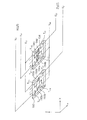
Images


Classifications
-
- G—PHYSICS
- G01—MEASURING; TESTING
- G01P—MEASURING LINEAR OR ANGULAR SPEED, ACCELERATION, DECELERATION, OR SHOCK; INDICATING PRESENCE, ABSENCE, OR DIRECTION, OF MOVEMENT
- G01P15/00—Measuring acceleration; Measuring deceleration; Measuring shock, i.e. sudden change of acceleration
- G01P15/02—Measuring acceleration; Measuring deceleration; Measuring shock, i.e. sudden change of acceleration by making use of inertia forces using solid seismic masses
- G01P15/08—Measuring acceleration; Measuring deceleration; Measuring shock, i.e. sudden change of acceleration by making use of inertia forces using solid seismic masses with conversion into electric or magnetic values
- G01P15/105—Measuring acceleration; Measuring deceleration; Measuring shock, i.e. sudden change of acceleration by making use of inertia forces using solid seismic masses with conversion into electric or magnetic values by magnetically sensitive devices
-
- G—PHYSICS
- G01—MEASURING; TESTING
- G01P—MEASURING LINEAR OR ANGULAR SPEED, ACCELERATION, DECELERATION, OR SHOCK; INDICATING PRESENCE, ABSENCE, OR DIRECTION, OF MOVEMENT
- G01P15/00—Measuring acceleration; Measuring deceleration; Measuring shock, i.e. sudden change of acceleration
- G01P15/02—Measuring acceleration; Measuring deceleration; Measuring shock, i.e. sudden change of acceleration by making use of inertia forces using solid seismic masses
- G01P15/08—Measuring acceleration; Measuring deceleration; Measuring shock, i.e. sudden change of acceleration by making use of inertia forces using solid seismic masses with conversion into electric or magnetic values
- G01P15/0891—Measuring acceleration; Measuring deceleration; Measuring shock, i.e. sudden change of acceleration by making use of inertia forces using solid seismic masses with conversion into electric or magnetic values with indication of predetermined acceleration values
-
- G—PHYSICS
- G01—MEASURING; TESTING
- G01P—MEASURING LINEAR OR ANGULAR SPEED, ACCELERATION, DECELERATION, OR SHOCK; INDICATING PRESENCE, ABSENCE, OR DIRECTION, OF MOVEMENT
- G01P15/00—Measuring acceleration; Measuring deceleration; Measuring shock, i.e. sudden change of acceleration
- G01P15/18—Measuring acceleration; Measuring deceleration; Measuring shock, i.e. sudden change of acceleration in two or more dimensions
Description
本発明は、磁気抵抗効果(MR)素子を用いた加速度センサ用のばね部材、加速度センサ及びこの加速度センサを備えた磁気ディスクドライブ装置に関する。 The present invention relates to a spring member for an acceleration sensor using a magnetoresistive effect (MR) element, an acceleration sensor, and a magnetic disk drive apparatus including the acceleration sensor.
例えば携帯型パソコン、携帯電話、デジタルオーディオプレーヤ等の携帯機器に組み込まれるハードディスクドライブ(HDD)、又はそれ自体がストレージとして携帯されるHDD若しくはリムーバブルHDD等の磁気ディスクドライブ装置においては、落下衝撃によって磁気ヘッドと磁気記録媒体とが衝突することを防ぐために、落下した瞬間を検知し磁気ヘッドを磁気記録媒体面から退避させることが必要となる。このような落下の瞬間は、重力加速度のわずかな変化として検知することができる。 For example, in a hard disk drive (HDD) incorporated in a portable device such as a portable personal computer, a cellular phone, a digital audio player, or a magnetic disk drive device such as an HDD or a removable HDD that is carried as a storage device, a magnetic field is generated by a drop impact. In order to prevent the head and the magnetic recording medium from colliding with each other, it is necessary to detect the moment when the head is dropped and to retract the magnetic head from the surface of the magnetic recording medium. Such a moment of falling can be detected as a slight change in gravitational acceleration.
重力加速度のわずかな変化を検知するための加速度センサとして、錘をばねによって支え、そのばねに圧電素子を貼り付けることにより、錘からばねに印加される力の変化を検知する圧電素子型加速度センサが知られている(例えば、特許文献1)。 As an acceleration sensor for detecting slight changes in gravitational acceleration, a piezoelectric element type acceleration sensor that detects a change in force applied from a weight to a spring by supporting the weight with a spring and attaching a piezoelectric element to the spring. Is known (for example, Patent Document 1).
重力加速度の変化を錘の微小変位で検知する加速度センサとして、対向する可動電極と固定電極間の距離の加速度による変化をこれらの静電容量の変化として検出する静電容量型加速度センサも知られている(例えば、特許文献2)。 As an acceleration sensor that detects a change in gravitational acceleration by a minute displacement of a weight, a capacitive acceleration sensor that detects a change due to the acceleration of the distance between a movable electrode and a fixed electrode facing each other as a change in these capacitances is also known. (For example, Patent Document 2).
このような圧電素子型加速度センサや静電容量型加速度センサは、いずれも、ばね自体に、又はばねに取り付けた錘若しくはその近傍に信号を取り出すための電極を設ける必要があるため、配線の引き回しで構造が非常に複雑になる。また、小型化したばねや錘に微小配線を施すことは、過重な衝撃が印加された際に破損を招き、ばねの変位を妨げるので感度を向上する際の障害となっている。この傾向は、加速度センサ全体の小型化を図るほどより顕著となる。 Such a piezoelectric element type acceleration sensor and a capacitance type acceleration sensor all need to be provided with an electrode for taking out a signal on the spring itself, on the weight attached to the spring or in the vicinity thereof, and therefore the wiring is routed. The structure becomes very complicated. In addition, applying fine wiring to a miniaturized spring or weight causes damage when an excessive impact is applied, and hinders displacement of the spring, which is an obstacle to improving sensitivity. This tendency becomes more remarkable as the acceleration sensor as a whole is miniaturized.
従来の圧電素子型加速度センサや静電容量型加速度センサの上述したような不都合を解消できる加速度センサとして、捩れ及び撓みの弾性変形が容易な4本のステーによって支持されており三次元的な捩れを伴う振動が可能な振動子に、Z軸上に軸線を含ませた質点の永久磁石を取り付け、X軸及びY軸の上であって座標軸の原点周りの同心円上にそれぞれ中心を持つ4個以上のMR素子による検出素子を配置し、永久磁石からの磁界強度の変化をX軸上の2個のMR検出素子の出力電圧の相対差によりX軸方向の、Y軸上の2個のMR検出素子の出力電圧の相対差によりY軸方向の、及び全てのMR検出素子の出力電圧の総和によりZ軸方向の加速度をそれぞれ検出する加速度センサが提案されている(例えば、特許文献3)。 As an acceleration sensor that can eliminate the above-mentioned disadvantages of conventional piezoelectric element type acceleration sensors and capacitance type acceleration sensors, it is supported by four stays that are easy to torsionally and flexibly deform, and is a three-dimensional torsion. A permanent magnet with a mass point that includes an axis on the Z axis is attached to a vibrator that can vibrate with four axes, and each has a center on a concentric circle around the origin of the coordinate axis on the X and Y axes. The above MR elements are arranged, and the change in the magnetic field intensity from the permanent magnet is caused by the relative difference between the output voltages of the two MR detection elements on the X axis, and the two MRs on the Y axis in the X axis direction. There has been proposed an acceleration sensor that detects acceleration in the Y-axis direction based on the relative difference between the output voltages of the detection elements and in the Z-axis direction based on the sum of output voltages of all MR detection elements (for example, Patent Document 3).
特許文献3に記載された加速度センサでは、4本のステー、即ちばね、によって支えられた振動子に永久磁石を固着し、印加された加速度によって生じる回転モーメントをこれらステーの捩り応力で平衡させ、その時の永久磁石の角度変化から加速度検出を行なっている。 In the acceleration sensor described in Patent Document 3, a permanent magnet is fixed to a vibrator supported by four stays, that is, springs, and the rotational moment generated by the applied acceleration is balanced by the torsional stress of these stays. The acceleration is detected from the angle change of the permanent magnet at that time.
一般に、板ばねにおける捩り応力のばね係数は、曲げ応力のばね係数より大きく、従って、その変位は小さい。このため、特許文献3に記載の加速度センサのように、主に捩り応力を利用するばねを用いた場合、変位量が小さいので、加速度検出感度を高めることが難しい。変位量を大きくして感度を高めるためには、全体のばね面積を大きくする必要があり、これは加速度センサの小型化への要求と逆行するものである。 In general, the spring coefficient of torsional stress in a leaf spring is larger than the spring coefficient of bending stress, and therefore its displacement is small. For this reason, when using a spring that mainly uses torsional stress as in the acceleration sensor described in Patent Document 3, it is difficult to increase the acceleration detection sensitivity because the amount of displacement is small. In order to increase sensitivity by increasing the amount of displacement, it is necessary to increase the overall spring area, which is contrary to the demand for miniaturization of the acceleration sensor.
従って本発明の目的は、加速度センサの大幅な小型化が図れ、かつ小型化を図った場合にも、高感度の加速度検出を行なうことができる加速度センサ用ばね部材、加速度センサ及びこの加速度センサを備えた磁気ディスクドライブ装置を提供することにある。 Therefore, an object of the present invention is to provide a spring member for acceleration sensor, an acceleration sensor, and an acceleration sensor capable of performing highly sensitive acceleration detection even when the acceleration sensor can be greatly reduced in size and reduced in size. An object of the present invention is to provide a magnetic disk drive device provided.
本発明によれば、錘部材を兼用する磁界発生手段又は磁界検出手段が取り付けられる加速度センサ用ばね部材であって、支点を有すると共に支点から偏位した位置に錘部材が取り付けられるように構成されており、外部から印加される力に対して曲げ応力を発生させて錘部材を変位させる少なくとも1つの帯状板ばねを備えた加速度センサ用ばね部材が提供される。 According to the present invention, there is provided a spring member for an acceleration sensor to which a magnetic field generating means or a magnetic field detecting means that also serves as a weight member is attached, and is configured such that the weight member is attached to a position that has a fulcrum and deviates from the fulcrum. There is provided a spring member for an acceleration sensor provided with at least one strip-shaped leaf spring that generates a bending stress with respect to a force applied from the outside to displace the weight member.
外力に対抗して曲げ応力を発生させ平衡させることにより錘部材を変位させる帯状板ばねを用いているため、小型でかつ変位量が大きい、従って小型で感度の高いばね構造とすることができ、小型かつ高感度の加速度センサを提供することができる。 Since a strip-shaped leaf spring that displaces the weight member by generating and balancing a bending stress against the external force is used, the spring structure is small and has a large amount of displacement. A small and highly sensitive acceleration sensor can be provided.
少なくとも1つの帯状板ばねが2つの帯状板ばねからなり、各帯状板ばねが、一方の端部に支点を有すると共に他方の端部に錘部材が取り付けられるように構成されていることが好ましい。 It is preferable that at least one belt spring is composed of two belt springs, and each belt spring has a fulcrum at one end and a weight member attached to the other end.
少なくとも1つの帯状板ばねが、中央部に支点を有すると共に両方の端部に錘部材がそれぞれ取り付けられるように構成された1つの帯状板ばねからなることも好ましい。 It is also preferable that at least one strip-shaped leaf spring is composed of one strip-shaped leaf spring having a fulcrum at the center and a weight member attached to both ends.
本発明によれば、さらに、錘部材を兼用する磁界発生手段又は磁界検出手段が取り付けられる加速度センサ用ばね部材であって、中央部に支点を有する第1の帯状板ばねと、第1の帯状板ばねの両端に中央部がそれぞれ連結された2つの第2の帯状板ばねとを備えており、第2の帯状板ばねの各々の両端部に錘部材がそれぞれ取り付けられるように構成されており、第1の帯状板ばねは外部から印加される力に対して曲げ応力又は捩り応力を発生させて錘部材を変位させるように構成されており、第2の帯状板ばねは外部から印加される力に対して曲げ応力を発生させて錘部材を変位させるように構成されている加速度センサ用ばね部材が提供される。 According to the present invention, there is further provided a spring member for an acceleration sensor to which a magnetic field generating means or a magnetic field detecting means also serving as a weight member is attached, the first belt spring having a fulcrum at the center, and the first belt shape. Two leaf-shaped leaf springs having a central portion connected to both ends of the leaf spring, respectively, and weight members are respectively attached to both ends of the second belt-like leaf spring. The first belt spring is configured to displace the weight member by generating a bending stress or a torsional stress with respect to a force applied from the outside, and the second belt spring is applied from the outside. A spring member for an acceleration sensor configured to generate a bending stress with respect to a force and displace the weight member is provided.
ここでは、外力に対抗して主に曲げ応力を発生させ平衡させることにより錘部材を変位させる帯状板ばねを用いているため、小型でかつ変位量が大きい、従って小型で感度の高いばね構造とすることができ、小型かつ高感度の加速度センサを提供することができる。 Here, since a strip-shaped leaf spring is used to displace the weight member by generating and balancing mainly bending stress against external force, the spring structure is small and has a large amount of displacement. Thus, a small and highly sensitive acceleration sensor can be provided.
また、2つの第2の帯状板ばねの各々又は各第2の帯状板ばねの両端部に取り付けられた錘部材に固着されており、各第2の帯状板ばねのばね動作を抑制する帯状支持部材をさらに備えていることが好ましい。 Further, each of the two second belt springs is fixed to a weight member attached to each end of each second belt spring or each of the second belt springs, and the belt support for suppressing the spring action of each second belt spring. It is preferable to further include a member.
本発明によれば、さらに、ハウジング部材と、磁界発生錘部材と、ハウジング部材に支点が取り付けられたばね部材と、磁界発生錘部材に対向してハウジング部材に取り付けられている磁界検出センサとを備えており、ばね部材が、支点から偏位した位置で磁界発生錘部材を固着しており、外部から印加される力に対して曲げ応力を発生させて磁界発生錘部材を変位させる少なくとも1つの帯状板ばねを有している加速度センサが提供される。 According to the present invention, it further includes a housing member, a magnetic field generating weight member, a spring member having a fulcrum attached to the housing member, and a magnetic field detection sensor attached to the housing member so as to face the magnetic field generating weight member. And the spring member is fixed to the magnetic field generating weight member at a position deviated from the fulcrum, and at least one belt-like member that generates a bending stress with respect to an externally applied force to displace the magnetic field generating weight member. An acceleration sensor having a leaf spring is provided.
ばね部材として、外力に対抗して曲げ応力を発生させ平衡させることにより錘部材を変位させる帯状板ばねを用いているため、小型かつ高感度の加速度センサを提供することができる。もちろん、ばね部材や磁界発生錘部材の部分に電極を設ける必要がないため、配線構造が簡単となる。また、磁界発生錘部材からのバイアス磁界を受けるため、外部電界及び外部磁界の影響を受けにくい。 As the spring member, a belt-like plate spring that displaces the weight member by generating and balancing a bending stress against an external force is used, and thus a small and highly sensitive acceleration sensor can be provided. Of course, since it is not necessary to provide electrodes on the spring member and the magnetic field generating weight member, the wiring structure is simplified. Further, since it receives a bias magnetic field from the magnetic field generating weight member, it is hardly affected by an external electric field and an external magnetic field.
ばね部材の少なくとも1つの帯状板ばねが2つの帯状板ばねからなり、各帯状板ばねが、一方の端部に支点を有すると共に他方の端部に磁界発生錘部材が取り付けられるように構成されていることが好ましい。 At least one strip-shaped leaf spring of the spring member is composed of two strip-shaped leaf springs, and each strip-shaped leaf spring has a fulcrum at one end and a magnetic field generating weight member is attached to the other end. Preferably it is.
ばね部材の少なくとも1つの帯状板ばねが、中央部に支点を有すると共に両方の端部に磁界発生錘部材がそれぞれ取り付けられるように構成された1つの帯状板ばねからなることも好ましい。 It is also preferable that at least one strip-shaped leaf spring of the spring member is composed of one strip-shaped leaf spring configured to have a fulcrum at the central portion and to be attached with magnetic field generating weight members at both ends.
磁界検出センサが磁化固定層及び磁化自由層を含みかつ磁化固定層が少なくとも1つの帯状板ばねの変位方向と平行な方向に磁化固定された少なくとも1対の多層構造MR素子を備えており、磁界発生錘部材が少なくとも1つの永久磁石を備えており、外部から力が印加されていない時に少なくとも1対の多層構造MR素子の積層面とほぼ垂直な方向に磁界が印加されるように構成されていることが好ましい。 The magnetic field detection sensor includes a magnetization fixed layer and a magnetization free layer, and the magnetization fixed layer includes at least one pair of multilayer structure MR elements in which magnetization is fixed in a direction parallel to a displacement direction of at least one strip-shaped leaf spring, The generating weight member includes at least one permanent magnet, and is configured such that when a force is not applied from the outside, a magnetic field is applied in a direction substantially perpendicular to the laminated surface of at least one pair of multilayer structure MR elements. Preferably it is.
本発明によれば、さらに、ハウジング部材と、4つの磁界発生錘部材と、ハウジング部材に支点が取り付けられたばね部材と、4つの磁界発生錘部材のうちの少なくとも3つに対向してハウジング部材にそれぞれ取り付けられている少なくとも3つの磁界検出センサとを備えており、ばね部材が、中央部に支点を有する第1の帯状板ばねと、第1の帯状板ばねの両端に中央部がそれぞれ連結された2つの第2の帯状板ばねとを有しており、2つの第2の帯状板ばねの両端部に4つの磁界発生錘部材がそれぞれ取り付けらており、第1の帯状板ばねは外部から印加される力に対して曲げ応力又は捩り応力を発生させて磁界発生錘部材を変位させるように構成されており、第2の帯状板ばねは外部から印加される力に対して曲げ応力を発生させて磁界発生錘部材を変位させるように構成されている加速度センサが提供される。 According to the present invention, the housing member, the four magnetic field generating weight members, the spring member having a fulcrum attached to the housing member, and the housing member facing at least three of the four magnetic field generating weight members. Each having at least three magnetic field detection sensors attached thereto, the spring member having a first strip-shaped leaf spring having a fulcrum at the central portion, and the central portion being coupled to both ends of the first strip-shaped leaf spring. And two magnetic field generating weight members are attached to both ends of the two second belt springs, respectively, and the first belt spring is externally provided. It is configured to generate a bending stress or a torsional stress with respect to an applied force to displace the magnetic field generating weight member, and the second strip leaf spring generates a bending stress with respect to an externally applied force. Let me An acceleration sensor that is configured to displace the field generation members with weights is provided.
ここでは、ばね部材として、外力に対抗して主に曲げ応力を発生させ平衡させることにより錘部材を変位させる帯状板ばねを用いているため、小型かつ高感度の加速度センサを提供することができる。2つの第2の帯状板ばね又は帯状支持部材の4つの端部を同一形状にすれば、X、Y及びZの3軸の感度及び指向性が揃った加速度センサを提供することができる。もちろん、ばね部材や磁界発生錘部材の部分に電極を設ける必要がないため、配線構造が簡単となる。また、磁界検出センサは磁界発生錘部材からのバイアス磁界を受けるため、外部電界及び外部磁界の影響を受けにくい。 Here, as the spring member, a strip-shaped plate spring that displaces the weight member by mainly generating and balancing a bending stress against an external force is used, so that a small and highly sensitive acceleration sensor can be provided. . If the four end portions of the two second strip-shaped leaf springs or strip-shaped support members have the same shape, it is possible to provide an acceleration sensor having the same X-axis, Y-axis, and Z-axis sensitivity and directivity. Of course, since it is not necessary to provide electrodes on the spring member and the magnetic field generating weight member, the wiring structure is simplified. Further, since the magnetic field detection sensor receives a bias magnetic field from the magnetic field generating weight member, it is not easily influenced by the external electric field and the external magnetic field.
また、磁界検出センサが磁化固定層及び磁化自由層を含みかつ磁化固定層が少なくとも1つの帯状板ばね又は帯状板ばねの変位方向と平行な方向に磁化固定された少なくとも1対の多層構造MR素子を備えており、磁界発生錘部材が少なくとも1つの永久磁石を備えており、外部から力が印加されていない時に少なくとも1対の多層構造MR素子の積層面とほぼ垂直な方向に磁界が印加されるように構成されていることが好ましい。磁化固定層が帯状板ばねの変位方向と平行な方向に磁化固定されているため、この方向へのバイアス磁界の変化のみがその多層構造MR素子によって検出されることとなるので、X軸方向及びY軸方向の加速度を独立して検出することが可能となる。また、磁界検出センサとして磁化固定層及び磁化自由層を含む多層構造MR素子、例えば、巨大磁気抵抗効果(GMR)素子又はトンネル磁気抵抗効果(TMR)素子を用いて磁化ベクトル検出を行なっているので、検出したい各方向における加速度の向き及び大きさを1つの磁界検出センサで検出することができる。従って、磁界検出センサ数が低減でき構造を非常に簡単化できるから、加速度センサを小型化することができる。さらに、GMR素子やTMR素子は磁気検出感度が非常に高いので、高感度の加速度検出を行なうことが可能となる。さらにまた、圧電素子型加速度センサや静電容量型加速度センサに比して低インピーダンスであるため、外乱の影響を受けにくい。 In addition, the magnetic field detection sensor includes a magnetization fixed layer and a magnetization free layer, and the magnetization fixed layer is at least one pair of multilayer structure MR elements in which the magnetization is fixed in a direction parallel to the displacement direction of the strip leaf spring. The magnetic field generating weight member includes at least one permanent magnet, and when a force is not applied from the outside, a magnetic field is applied in a direction substantially perpendicular to the laminated surface of at least one pair of multilayer structure MR elements. It is preferable that it is comprised so that. Since the magnetization fixed layer is magnetization fixed in the direction parallel to the displacement direction of the strip-shaped leaf spring, only the change of the bias magnetic field in this direction is detected by the multilayer MR element, The acceleration in the Y-axis direction can be detected independently. Further, since the magnetic field detection sensor uses a multilayer structure MR element including a magnetization fixed layer and a magnetization free layer, for example, a giant magnetoresistance effect (GMR) element or a tunnel magnetoresistance effect (TMR) element, magnetization vector detection is performed. The direction and magnitude of acceleration in each direction to be detected can be detected by one magnetic field detection sensor. Therefore, since the number of magnetic field detection sensors can be reduced and the structure can be greatly simplified, the acceleration sensor can be miniaturized. Further, since the GMR element and the TMR element have extremely high magnetic detection sensitivity, it is possible to perform highly sensitive acceleration detection. Furthermore, since it has a lower impedance than a piezoelectric element type acceleration sensor or a capacitance type acceleration sensor, it is less susceptible to disturbances.
2つの第2の帯状板ばねの各々又は各第2の帯状板ばねの両端部に取り付けられた2つの磁界発生錘部材に固着されており、各第2の帯状板ばねのばね動作を抑制する帯状支持部材をさらに備えていることが好ましい。 Each of the two second belt springs is fixed to two magnetic field generating weight members attached to both ends of each second belt spring or each of the second belt springs, and suppresses the spring action of each second belt spring. It is preferable to further include a belt-like support member.
少なくとも1つの永久磁石が、磁界検出センサに対向する面が互いに逆極性となるように並列配置された1対の永久磁石からなることも好ましい。 It is also preferable that at least one permanent magnet is composed of a pair of permanent magnets arranged in parallel so that the surfaces facing the magnetic field detection sensor have opposite polarities.
少なくとも1対の多層構造MR素子が、1対の永久磁石にそれぞれ対向して配置されていることも好ましい。 It is also preferable that at least one pair of multi-layered MR elements are respectively arranged to face a pair of permanent magnets.
多層構造MR素子が、GMR素子又はTMR素子であることが好ましい。 The multilayer structure MR element is preferably a GMR element or a TMR element.
本発明によれば、さらにまた、上述した加速度センサを備えた磁気ディスクドライブ装置が提供される。 According to the present invention, there is further provided a magnetic disk drive device provided with the acceleration sensor described above.
本発明によれば、外力に対抗して曲げ応力を発生させ平衡させることにより錘部材を変位させる帯状板ばねを用いているため、小型でかつ変位量が大きい、従って小型で感度の高いばね構造とすることができ、小型かつ高感度の加速度センサを提供することができる。 According to the present invention, since the strip-shaped leaf spring that displaces the weight member by generating and balancing the bending stress against the external force is used, the spring structure is small and has a large displacement, and thus is small and highly sensitive. Thus, a small and highly sensitive acceleration sensor can be provided.
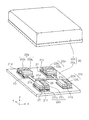
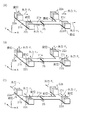
図1は加速度センサを組み込んだ磁気ディスクドライブ装置の一例の全体構成を概略的に示す斜視図である。この磁気ディスクドライブ装置は、例えば2.5インチ、1.8インチ、1.3インチ又は1インチ以下の磁気ディスクを用いる超小型HDDであり、例えば携帯型パソコン、携帯電話、デジタルオーディオプレーヤ等の携帯機器に組み込まれるHDD又はそれ自体がストレージとして携帯されるHDD若しくはリムーバブルHDDである。 FIG. 1 is a perspective view schematically showing an overall configuration of an example of a magnetic disk drive device incorporating an acceleration sensor. This magnetic disk drive device is an ultra-small HDD using a magnetic disk of 2.5 inches, 1.8 inches, 1.3 inches or 1 inch or less, for example, a portable personal computer, a mobile phone, a digital audio player, etc. The HDD incorporated in the portable device or the HDD itself or a removable HDD carried as storage.
同図は磁気ディスクドライブ装置の蓋を外した状態を示しており、10は動作時にスピンドルモータにより回転する磁気ディスク、10aは落下検出時に磁気ヘッドが移動するデータの書き込まれていない退避ゾーン、11は動作時に磁気ディスク10の表面に対向する磁気ヘッドを先端部に有するヘッドジンバルアセンブリ(HGA)、12は磁気ヘッドに電気的に接続された配線部材であるフレクシブル回路(FPC)、13はHGA11を支持する支持アーム、14は支持アーム13を回動軸15を中心に回動させて位置決めするためのアクチュエータであるボイスコイルモータ(VCM)、16は落下検出時に支持アーム13の爪13aが乗り上げて磁気ヘッドを磁気ディスク表面から離れるための退避ランプ、17は回路基板18上に搭載された加速度センサをそれぞれ示している。
This figure shows a state in which the lid of the magnetic disk drive device is removed, 10 is a magnetic disk that is rotated by a spindle motor during operation, 10a is a retreat zone in which no data is written, and the magnetic head moves when a drop is detected, 11 Is a head gimbal assembly (HGA) having a magnetic head facing the surface of the
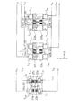
図2は本発明の加速度センサの一実施形態における全体構成を概略的に示す分解斜視図であり、図3はハウジング部材の内部に設けられるばね部材、磁界発生錘部材及び磁界検出センサチップの構成を概略的に示す分解斜視図である。 FIG. 2 is an exploded perspective view schematically showing the overall configuration of one embodiment of the acceleration sensor of the present invention, and FIG. 3 is a configuration of a spring member, a magnetic field generating weight member, and a magnetic field detection sensor chip provided inside the housing member. It is a disassembled perspective view which shows schematically.
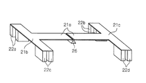
これらの図に示すように、本実施形態における加速度センサは、X軸方向、Y軸方向及びZ軸方向の3軸加速度を検出するためのものであり、ハウジング部材20内に、第1の帯状板ばね21a、2つの第2の帯状板ばね21b及び21c並びに磁界発生錘部材を支持するための4つの錘支持部21d〜21gを一体的に形成してなるばね部材21と、永久磁石の伸長方向を除いて寸法、形状及び重量等の構成が共に同じである4つの磁界発生錘部材22a〜22dと、X軸Z軸用の第1の磁界検出センサチップ23と、X軸Z軸用の第2の磁界検出センサチップ24と、Y軸用の第3の磁界検出センサチップ25と、支点部材26とを収納するように構成されている。
As shown in these drawings, the acceleration sensor in the present embodiment is for detecting three-axis acceleration in the X-axis direction, the Y-axis direction, and the Z-axis direction. The
ハウジング部材20は、基板自体が例えばポリイミド又はBTレジン等の樹脂材料による平板形状の基板に配線パターン(図示なし)を設けることで形成された配線基板20aと、この配線基板20aを覆って密封する磁性金属材料によって形成されたカバー部材20bとから構成されている。本実施形態では、X軸方向、Y軸方向及びZ軸方向の3軸加速度を、配線基板20aによる1平面上に搭載した3つの磁界検出センサチップ23〜25で検出することが可能となる。
The
ばね部材21は、例えばNiFeやNi等による薄膜金属板か、ステンレス鋼等の薄板か、又はポリイミド等による薄い樹脂板を、本実施形態では、図3に示すように形状加工することによって一体的に形成されている。
In this embodiment, the
第1の帯状板ばね21aは主ばねを構成しており、外部から印加される力に対して曲げ応力及び/又は捩り応力を発生させる。第1の帯状板ばね21aの中央部は支点を構成しており、この中央部は一端が配線基板20aに固着されている支点部材26の他端に固着されている。2つの第2の帯状板ばね21b及び21cは副ばねを構成しており、外部から印加される力に対して曲げ応力のみを発生させる。これら第2の帯状板ばね21b及び21cは、中央部が第1の帯状板ばね21aの両端にそれぞれ一体的に連結されている。第2の帯状板ばね21b及び21cの両端は互いに同一形状の錘支持部21d〜21gにそれぞれ一体的に連結されている。なお、錘支持部21d〜21gは図では矩形であるが、円形であってもその他の形状であっても良い。
The first strip-shaped
磁界発生錘部材22a〜22dは、ばね部材21の錘支持部21d〜21gの一方の面(磁界センサチップに対向する面とは反対側の面)上にそれぞれ接着剤で固着されている。磁界発生錘部材22a〜22dは、それぞれ、磁界発生用の1対の永久磁石22a1及び22a2、22b1及び22b2、22c1及び22c2、並びに22d1及び22d2から構成されている。
The magnetic field generating
X軸Z軸用の第1の磁界検出センサチップ23、X軸Z軸用の第2の磁界検出センサチップ24及びY軸用の第3の磁界検出センサチップ25は、4つの磁界発生錘部材22a〜22dのうちの3つの磁界発生錘部材22a〜22cにそれぞれ対向して、具体的には錘支持部21d〜21fの他方の面にそれぞれ対向して、配線基板20a上に接着剤で固着されている。従って、磁界発生錘部材22a〜22cは、加速度に応じて角度の変化する磁界を第1〜第3の磁界検出センサチップ23〜25にそれぞれ印加することとなる。なお、本実施形態では、磁界発生錘部材22dは、ばね部材21の平衡を保つことのみを目的として設けられている。
The first magnetic field
1対の永久磁石22a1及び22a2は、X軸方向に互いに平行に伸長する直方体形状のフェライト材料で形成されており、X軸Z軸用の第1の磁界検出センサチップ23に対向している。これら1対の永久磁石22a1及び22a2は、第1の磁界検出センサチップ23に対向する面が互いに逆極性となるように配置されているおり、両者で閉磁路を構成している。後述するように、第1の磁界検出センサチップ23のスピンバルブGMR素子がこの閉磁路内にその積層面とほぼ垂直な方向に磁界(バイアス磁界)が印加されるように配置される。
The pair of
1対の永久磁石22b1及び22b2は、X軸方向に互いに平行に伸長する直方体形状のフェライト材料で形成されており、X軸Z軸用の第2の磁界検出センサチップ24に対向している。これら1対の永久磁石22b1及び22b2は、第2の磁界検出センサチップ24に対向する面が互いに逆極性となるように配置されているおり、両者で閉磁路を構成している。後述するように、第2の磁界検出センサチップ24のスピンバルブGMR素子がこの閉磁路内にその積層面とほぼ垂直な方向にバイアス磁界が印加されるように配置される。
The pair of
1対の永久磁石22c1及び22c2は、Y軸方向に互いに平行に伸長する直方体形状のフェライト材料で形成されており、Y軸用の第3の磁界検出センサチップ25に対向している。これら1対の永久磁石22c1及び22c2は、第3の磁界検出センサチップ25に対向する面が互いに逆極性となるように配置されているおり、両者で閉磁路を構成している。後述するように、第3の磁界検出センサチップ25のスピンバルブGMR素子がこの閉磁路内にその積層面とほぼ垂直な方向にバイアス磁界が印加されるように配置される。
The pair of
図4は本実施形態の加速度センサにおける配線基板上の結線及び磁界検出センサチップの構成を概略的に示す図であり、図5は本実施形態の加速度センサにおける配線基板及び磁界検出センサチップの電気的構成を概略的に示す回路図であり、図6は本実施形態の加速度センサにおける等価回路図である。 FIG. 4 is a diagram schematically showing the connection on the wiring board and the configuration of the magnetic field detection sensor chip in the acceleration sensor of this embodiment, and FIG. 5 is an electrical diagram of the wiring board and the magnetic field detection sensor chip in the acceleration sensor of this embodiment. FIG. 6 is an equivalent circuit diagram of the acceleration sensor according to the present embodiment.
これらの図に示すように、X軸Z軸方向の加速度を検出するための第1の磁界検出センサチップ23には、X軸方向と垂直な方向(Y軸方向)に沿った直線部分を有する4つ(2対)のスピンバルブGMR素子23a、23b、23c及び23dが互いに平行に形成されている。スピンバルブGMR素子23a及び23bは対となっており、互いに直列接続されている。その直列接続の両端が電源端子電極TVCC及びTVDDにそれぞれ接続されており、中点が信号出力端子TX1に接続されている。スピンバルブGMR素子23c及び23dも対となっており、互いに直列接続されている。その直列接続の両端が電源端子電極TVCC及びTVDDにそれぞれ接続されており、中点が信号出力端子TZ1に接続されている。
As shown in these drawings, the first magnetic field
スピンバルブGMR素子23a、23b、23c及び23dの各々は、基本的には、反強磁性材料によるピン層及び強磁性材料によるピンド層からなる磁化固定層と、非磁性中間層と、強磁性材料による磁化自由層(フリー層)とを積層した多層構造を有しており、ピンド層がフリー層の延在方向と垂直な同一方向に磁化固定されている。即ち、これらスピンバルブGMR素子23a、23b、23c及び23dのピンド層は、全てX軸方向の同一向きに磁化固定されている。
Each of the spin
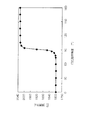
図7はスピンバルブGMR素子の積層面への印加磁界角度に対するMR抵抗変化特性を表す図である。同図において、横軸は印加磁界のフリー層の延在方向(磁化固定方向と垂直な方向)となす角度(°)、縦軸はMR抵抗(Ω)をそれぞれ表している。同図から分かるように、MR抵抗はバイアス磁界が90°近傍で僅かに変化しても大きく変化する。バイアス磁界の微小角度θの変化は90±θであるから、磁界発生錘部材の、従って1対の永久磁石の僅かな傾きが抵抗変化として取り出され、しかも、磁化ベクトルとして、大きさのみならずその正負の方向も取り出せることとなる。 FIG. 7 is a graph showing MR resistance change characteristics with respect to the applied magnetic field angle to the laminated surface of the spin valve GMR element. In the figure, the horizontal axis represents the angle (°) formed with the extending direction of the free layer of the applied magnetic field (direction perpendicular to the magnetization fixed direction), and the vertical axis represents the MR resistance (Ω). As can be seen from the figure, the MR resistance changes greatly even if the bias magnetic field changes slightly in the vicinity of 90 °. Since the change in the minute angle θ of the bias magnetic field is 90 ± θ, a slight inclination of the magnetic field generating weight member, and thus a pair of permanent magnets, is taken out as a resistance change, and not only the magnitude as a magnetization vector. The positive and negative directions can also be taken out.
互いに直列接続された対となるスピンバルブGMR素子23a及び23bのピンド層が同一方向に磁化固定されるのは、対となるスピンバルブGMR素子の各々に印加されるバイアス磁界が互いにほぼ逆方向であるためである。即ち、図5に示すように、1対の永久磁石22a1及び22a2によって閉磁路が構成されており、対となるスピンバルブGMR素子23a及び23bが、閉磁路の逆方向磁界が流れる磁路内に配置されているからバイアス磁界が互いにほぼ逆方向となるのである。互いに直列接続された対となるスピンバルブGMR素子23c及び23dについても同様である。この場合、閉磁路を構成する磁気回路の中心が、対となるスピンバルブGMR素子間の中心線上に位置していることとなる。
The pinned layers of the paired spin
このように、互いにほぼ逆方向のバイアス磁界が印加されることにより、対をなすスピンバルブGMR素子23a及び23b並びに23c及び23dのピンド層の磁化固定方向が同一方向となるので、これら対をなす4つのスピンバルブGMR素子を1つのチップ内に形成することができ、その結果、加速度センサ全体のさらなる小型化を図ることが可能となる。
Thus, by applying bias magnetic fields in substantially opposite directions, the pinned layers of the spin
X軸Z軸方向の加速度を検出するための第2の磁界検出センサチップ24にも、X軸方向と垂直な方向(Y軸方向)に沿った直線部分を有する4つ(2対)のスピンバルブGMR素子24a、24b、24c及び24dが互いに平行に形成されている。スピンバルブGMR素子24b及び24aは対となっており、互いに直列接続されている。その直列接続の両端が電源端子電極TVCC及びTVDDにそれぞれ接続されており、中点が信号出力端子TX2接続されている。スピンバルブGMR素子24c及び24dも対となっており、互いに直列接続されている。その直列接続の両端が電源端子電極TVCC及びTVDDにそれぞれ接続されており、中点が信号出力端子TZ2接続されている。
The second magnetic field
スピンバルブGMR素子24a、24b、24c及び24dの各々は、基本的には、反強磁性材料によるピン層及び強磁性材料によるピンド層からなる磁化固定層と、非磁性中間層と、強磁性材料による磁化自由層(フリー層)とを積層した多層構造を有しており、ピンド層がフリー層の延在方向と垂直な同一方向に磁化固定されている。即ち、これらスピンバルブGMR素子24a、24b、24c及び24dのピンド層は、全てX軸方向の同一向きに磁化固定されている。
Each of the spin
互いに直列接続された対となるスピンバルブGMR素子24a及び24bのピンド層が同一方向に磁化固定されるのは、対となるスピンバルブGMR素子の各々に印加されるバイアス磁界が互いにほぼ逆方向であるためである。即ち、図5に示すように、1対の永久磁石22b1及び22b2によって閉磁路が構成されており、対となるスピンバルブGMR素子24a及び24bが、閉磁路の逆方向磁界が流れる磁路内に配置されているからバイアス磁界が互いにほぼ逆方向となるのである。互いに直列接続された対となるスピンバルブGMR素子24c及び24dについても同様である。この場合、閉磁路を構成する磁気回路の中心が、対となるスピンバルブGMR素子間の中心線上に位置していることとなる。
The pinned layers of the paired spin
このように、互いにほぼ逆方向のバイアス磁界が印加されることにより、対をなすスピンバルブGMR素子24a及び24b並びに24c及び24dのピンド層の磁化固定方向が同一方向となるので、これら対をなす4つのスピンバルブGMR素子を1つのチップ内に形成することができ、その結果、加速度センサ全体のさらなる小型化を図ることが可能となる。
Thus, by applying bias magnetic fields in substantially opposite directions to each other, the pinned layers of the spin
Y軸方向の加速度を検出するための第3の磁界検出センサチップ25には、Y軸方向と垂直な方向(X軸方向)に沿った直線部分を有する4つ(2対)のスピンバルブGMR素子25a、25b、25c及び25dが互いに平行に形成されている。スピンバルブGMR素子25a及び25bは対となっており、互いに直列接続されている。その直列接続の両端が電源端子電極TVCC及びTVDDにそれぞれ接続されており、中点が信号出力端子TY1接続されている。スピンバルブGMR素子25c及び25dも対となっており、互いに直列接続されている。その直列接続の両端が電源端子電極TVCC及びTVDDにそれぞれ接続されており、中点が信号出力端子TY2接続されている。
The third magnetic field
スピンバルブGMR素子25a、25b、25c及び25dの各々は、基本的には、反強磁性材料によるピン層及び強磁性材料によるピンド層からなる磁化固定層と、非磁性中間層と、強磁性材料による磁化自由層(フリー層)とを積層した多層構造を有しており、ピンド層がフリー層の延在方向と垂直な同一方向に磁化固定されている。即ち、これらスピンバルブGMR素子25a、25b、25c及び25dのピンド層は、全てY軸方向の同一向きに磁化固定されている。
Each of the spin
互いに直列接続された対となるスピンバルブGMR素子25a及び25bのピンド層が同一方向に磁化固定されるのは、対となるスピンバルブGMR素子の各々に印加されるバイアス磁界が互いにほぼ逆方向であるためである。即ち、図5に示すように、1対の永久磁石22c1及び22c2によって閉磁路が構成されており、対となるスピンバルブGMR素子25a及び25bが、閉磁路の逆方向磁界が流れる磁路内に配置されているからバイアス磁界が互いにほぼ逆方向となるのである。互いに直列接続された対となるスピンバルブGMR素子25c及び25dについても同様である。この場合、閉磁路を構成する磁気回路の中心が、対となるスピンバルブGMR素子間の中心線上に位置していることとなる。
The pinned layers of the paired spin
このように、互いにほぼ逆方向のバイアス磁界が印加されることにより、対をなすスピンバルブGMR素子25a及び25b並びに25c及び25dのピンド層の磁化固定方向が同一方向となるので、これら対をなす4つのスピンバルブGMR素子を1つのチップ内に形成することができ、その結果、加速度センサ全体のさらなる小型化を図ることが可能となる。
Thus, by applying bias magnetic fields in substantially opposite directions to each other, the pinned layers of the spin
第1の磁界検出センサチップ23のスピンバルブGMR素子23a及び23b間には電源電圧Vcc−Vddが印加され、その中点に接続された信号出力端子TX1から第1のX軸方向加速度信号VX1が取り出される。また、第2の磁界検出センサチップ24のスピンバルブGMR素子24b及び24a間には電源電圧Vcc−Vddが印加され、その中点に接続された信号出力端子TX2から第2のX軸方向加速度信号VX2が取り出される。従って、これらスピンバルブGMR素子23a及び23b並びにスピンバルブGMR素子24b及び24aは、図6(A)に示すようにフルブリッジ接続されていることとなり、信号出力端子TX1及び信号出力端子TX2からの信号VX1及びVX2が差動増幅されてX軸方向の加速度信号となる。このX軸方向の加速度信号は、印加される加速度の方向によって、磁界発生錘部材22a(従って永久磁石22a1及び22a2)と磁界発生錘部材22b(従って永久磁石22b1及び22b2)とがZ軸の互いに反対方向に変位した際にのみ出力され、共に同じ方向に変位した際には第1のX軸方向加速度信号VX1及び第2のX軸方向加速度信号VX2が互いに打ち消し合って出力されない。
A power supply voltage Vcc-Vdd is applied between the spin
第1の磁界検出センサチップ23のスピンバルブGMR素子23c及び23d間には電源電圧Vcc−Vddが印加され、その中点に接続された信号出力端子TZ1から第1のZ軸方向加速度信号VZ1が取り出される。また、第2の磁界検出センサチップ24のスピンバルブGMR素子24c及び24d間には電源電圧Vcc−Vddが印加され、その中点に接続された信号出力端子TZ2から第2のZ軸方向加速度信号VZ2が取り出される。従って、これらスピンバルブGMR素子23c及び23d並びにスピンバルブGMR素子24c及び24dは、図6(B)に示すようにフルブリッジ接続されていることとなり、信号出力端子TZ1及び信号出力端子TZ2からの信号VZ1及びVZ2が差動増幅されてZ軸方向の加速度信号となる。このZ軸方向の加速度信号は、印加される加速度によって、磁界発生錘部材22a(従って永久磁石22a1及び22a2)と磁界発生錘部材22b(従って永久磁石22b1及び22b2)とがZ軸の共に同じ方向に変位した際にのみ出力され、互いに反対方向に変位した際には第1のZ軸方向加速度信号VZ1及び第2のZ軸方向加速度信号VZ2が互いに打ち消し合って出力されない。
A power supply voltage Vcc-Vdd is applied between the spin
第3の磁界検出センサチップ25のスピンバルブGMR素子25b及び25a間には電源電圧Vcc−Vddが印加され、その中点に接続された信号出力端子TY1から第1のY軸方向加速度信号VY1が取り出され、スピンバルブGMR素子25c及び25d間には電源電圧Vcc−Vddが印加され、その中点に接続された信号出力端子TY2から第2のY軸方向加速度信号VY2が取り出される。従って、この第3の磁界検出センサチップ25のスピンバルブGMR素子25a〜25dは、図6(C)に示すようにフルブリッジ接続されていることとなり、信号出力端子TY1及び信号出力端子TY2からの信号VY1及びVY2が差動増幅されてY軸方向の加速度信号となる。このY軸方向の加速度信号は、印加される加速度によって、磁界発生錘部材22c(従って永久磁石22c1及び22c2)がZ軸方向に変位した際に出力される。
A power supply voltage Vcc-Vdd is applied between the spin
次に、本実施形態におけるばね部材21についてより詳細に説明する。
Next, the
図8は本発明のばね部材における帯状板ばねの基本的な動作を説明する図である。 FIG. 8 is a view for explaining the basic operation of the strip-shaped leaf spring in the spring member of the present invention.
同図(A)は外力が印加されていない場合であり、80は帯状板ばね、81はその一方の端に位置する曲げ中心又は支点、82は曲げ中心81から偏位した位置である、帯状板ばね80の他方の端部の一面に固着された錘部材をそれぞれ示している。以下の説明のために、帯状板ばね80の面と垂直な方向を曲げ方向、帯状板ばね80の縦方向を長さ方向と定義する。
FIG. 6A shows a case where no external force is applied, 80 is a belt-like leaf spring, 81 is a bending center or fulcrum located at one end thereof, and 82 is a position displaced from the bending
同図(B)に示すように曲げ方向に外力が印加された場合及び同図(C)に示すように長さ方向に外力が印加された場合のいずれにも、帯状板ばね80は曲げ応力を発生させ、その端部及び錘部材82は曲げ方向に変位する。
The
図9は図8に示した帯状板ばねが曲げ中心から両側に2つ展開した構成の帯状板ばね、換言すれば、中央部に支点91を有し、両端部に錘部材92a及び92bが取り付けられた帯状板ばね90の動作を説明する図である。
FIG. 9 is a belt spring having a configuration in which the belt spring shown in FIG. 8 is developed on both sides from the bending center, in other words, it has a fulcrum 91 at the center and
同図(A)は曲げ方向に外力Fzが印加された場合であり、この場合に帯状板ばね90の両端部及び錘部材92a及び92bは共に同一の曲げ方向に変位する。一方、同図(B)は長さ方向に外力Fxが印加された場合であり、この場合に帯状板ばね90の両端部及び錘部材92a及び92bは互いに反対の曲げ方向に変位する。ここで、同図(A)の外力Fzと同図(B)の外力Fxとが、|Fz|=|Fx|の場合には、錘部材92a及び92bの変位量は等しくなる。錘部材92a及び92bの変位量は、錘部材92a及び92bの変位角θに比例する。錘部材を磁界を発生する永久磁石とすれば、スピンバルブGMR素子は、この変位角θを検出して印加される外力を検出することができる。
FIG. 6A shows a case where an external force Fz is applied in the bending direction. In this case, both ends of the belt-
図10は本実施形態におけるばね部材の動作を説明するための図である。ただし、図10では、磁界発生錘部材22c及び22dの伸長方向が本実施形態と異なって表されているが、ばね部材としての動作は同じである。
FIG. 10 is a view for explaining the operation of the spring member in the present embodiment. However, in FIG. 10, the extension directions of the magnetic field generating
同図(A)に示すように、X軸方向の外力Fxが印加されると、主ばねである第1の帯状板ばね21a及び副ばねである第2の帯状板ばね21b及び21cが共に曲げ応力を発生させ、平衡が保たれる位置まで主ばねの曲げ方向に変位する。この場合、磁界発生錘部材22a及び22cと磁界発生錘部材22b及び22dとの変位方向は互いに逆方向である。同図(B)に示すように、Z軸方向の外力Fzが印加されると、主ばねである第1の帯状板ばね21a及び副ばねである第2の帯状板ばね21b及び21cが共に曲げ応力を発生させ、平衡が保たれる位置まで主ばねの曲げ方向に変位する。ただし、この場合、磁界発生錘部材22a及び22cと磁界発生錘部材22b及び22dとの変位方向は共に同じ方向である。さらに、同図(C)に示すように、Y軸方向の外力Fyが印加されると、主ばねである第1の帯状板ばね21aはその長さ方向の中心を軸として回転する捩れ応力を発生させ、副ばねである第2の帯状板ばね21b及び21cは曲げ応力を発生させ、平衡が保たれる位置まで主ばねの長さ方向の中心を軸とした回転方向に変位する。この場合、磁界発生錘部材22a及び22bと磁界発生錘部材22c及び22dとの変位方向は互いに逆方向である。
As shown in FIG. 6A, when an external force Fx in the X-axis direction is applied, the first belt-
X軸方向の外力Fxが印加され、磁界発生錘部材22a及び22c並びに磁界発生錘部材22b及び22dが上述のごとく主ばねの曲げ方向に変位すると、スピンバルブGMR素子23a及び23b並びに24b及び24aに印加されるバイアス磁界の角度がこれに伴って同じ方向に変化し、第1のX軸方向加速度信号VX1及び第2のX軸方向加速度信号VX2を加算した差動出力が得られ、これがX軸方向の加速度信号となる。この場合、第1のZ軸方向加速度信号VZ1及び第2のZ軸方向加速度信号VZ2が互いに打ち消し合い、Z軸方向の加速度信号は出力されない。また、この場合、バイアス磁界の角度がスピンバルブGMR素子25d、25b、25c及び25aのフリー層の延在方向に沿って変化するため、第1のY軸方向加速度信号VY1及び第2のY軸方向加速度信号VY2は出力されず、従ってY軸方向の加速度信号は出力されない。
When an external force Fx in the X-axis direction is applied and the magnetic field generating
Z軸方向の外力Fzが印加され、磁界発生錘部材22a及び22c並びに磁界発生錘部材22b及び22dが上述のごとく主ばねの曲げ方向に変位すると、スピンバルブGMR素子23c及び23d並びに24c及び24dに印加されるバイアス磁界の角度がこれに伴って反対方向に変化し、第1のZ軸方向加速度信号VZ1及び第2のZ軸方向加速度信号VZ2を加算した差動出力が得られ、これがZ軸方向の加速度信号となる。この場合、第1のX軸方向加速度信号VX1及び第2のX軸方向加速度信号VX2が互いに打ち消し合い、X軸方向の加速度信号は出力されない。また、この場合、バイアス磁界の角度がスピンバルブGMR素子25d、25b、25c及び25aのフリー層の延在方向に沿って変化するため、第1のY軸方向加速度信号VY1及び第2のY軸方向加速度信号VY2は出力されず、従ってY軸方向の加速度信号は出力されない。
When an external force Fz in the Z-axis direction is applied and the magnetic field generating
Y軸方向の外力Fyが印加され、磁界発生錘部材22a及び22c並びに磁界発生錘部材22b及び22dが上述のごとく主ばねの長さ方向の中心を軸とした回転方向に変位すると、スピンバルブGMR素子25d、25b、25c及び25aに印加されるバイアス磁界の角度がこれに伴って同じ方向に変化し、第1のY軸方向加速度信号VY1及び第2のY軸方向加速度信号VY2を加算した差動出力が得られ、これがY軸方向の加速度信号となる。また、この場合、バイアス磁界の角度がスピンバルブGMR素子23a〜23d及び24a〜24dのフリー層の延在方向に沿って変化するため、第1のX軸方向加速度信号VX1及び第2のX軸方向加速度信号VX2並びに第1のZ軸方向加速度信号VZ1及び第2のZ軸方向加速度信号VZ2は出力されず、従ってX軸方向及びZ軸方向の加速度信号は出力されない。
When an external force Fy in the Y-axis direction is applied and the magnetic field generating
以上説明したように、本実施形態によれば、主ばねである第1の帯状板ばね21a及び副ばねである第2の帯状板ばね21b及び21cが共に曲げ応力を発生させ、平衡が保たれる位置まで変位するように構成されているため、小型でかつ変位量が大きい、従って小型で感度の高いばね構造とすることができ、小型かつ高感度の加速度センサを提供することができる。
As described above, according to the present embodiment, the first belt-
ばね部材の4つの端部の構造を同一形状とすることができるため、検出したい各方向(X軸方向、Y軸方向、Z軸方向)の感度、感度指向性が揃った加速度センサを提供することができる。 Since the structure of the four end portions of the spring member can have the same shape, an acceleration sensor having the sensitivity and sensitivity directivity in each direction (X-axis direction, Y-axis direction, Z-axis direction) to be detected is provided. be able to.
さらに本実施形態によれば、中央に支点を有し両端部に磁界発生錘部材をそれぞれ固着した第1の帯状板ばね21aの曲げ動作を利用すると共に、第1の磁界検出センサチップ23の一部出力VX1又はVZ1と第2の磁界検出センサチップ24の一部出力VX2又はVZ2との差動出力を取り出すようにしているので、X軸方向及びZ軸方向の加速度成分を確実に分離して正確に検出することができる。また、第1の帯状板ばね21aの捩り動作を利用すると共に、第3の磁界検出センサチップ25の磁界検出方向を工夫しているので、Y軸方向の加速度成分を確実に分離して正確に検出することができる。
Furthermore, according to the present embodiment, the bending operation of the first strip-shaped
また、X軸方向、Y軸方向、Z軸方向における加速度の向き及び大きさを3つの磁界検出センサチップで検出できるので、磁界検出センサチップ数が低減でき構造を非常に簡単化でき、加速度センサ全体を小型化することができる。また、スピンバルブGMR素子は磁気検出感度が非常に高いので、高感度の加速度検出を行なうことが可能となる。 In addition, since the direction and magnitude of acceleration in the X-axis direction, Y-axis direction, and Z-axis direction can be detected by three magnetic field detection sensor chips, the number of magnetic field detection sensor chips can be reduced, and the structure can be greatly simplified. The whole can be reduced in size. In addition, since the spin valve GMR element has a very high magnetic detection sensitivity, it is possible to detect acceleration with high sensitivity.
さらに、各磁界検出センサチップにおいて、互いにほぼ逆方向のバイアス磁界が印加されるため、対をなすスピンバルブGMR素子のピンド層の磁化固定方向が同一方向となりこれら対をなす4つのスピンバルブGMR素子を1つのチップ内に形成することができる。その結果、加速度センサ全体のさらなる小型化を図ることが可能となる。 Further, in each magnetic field detection sensor chip, bias magnetic fields in opposite directions are applied to each other, so that the pinned layer magnetization direction of the paired spin valve GMR elements becomes the same direction, and the four spin valve GMR elements forming these pairs Can be formed in one chip. As a result, the entire acceleration sensor can be further reduced in size.
さらにまた、本実施形態によれば、対となる2つの永久磁石によって、広い範囲に分布した垂直方向の磁界による閉磁路が形成され、スピンバルブGMR素子がこの閉磁路中に配置されるため、必要最小限の磁界しか閉磁路から外部へ漏れず、漏れ磁界が少なくなるから充分に大きなバイアス磁界が印加されることとなり、永久磁石が小型となった場合にも、加速度の検出感度が安定してかつ高くなり、しかも外部電界及び外部磁界の影響を受けにくくなる。 Furthermore, according to the present embodiment, a closed magnetic circuit is formed by a vertical magnetic field distributed over a wide range by two permanent magnets in a pair, and the spin valve GMR element is disposed in this closed magnetic circuit. Only the minimum necessary magnetic field leaks from the closed magnetic path to the outside, and since the leakage magnetic field is reduced, a sufficiently large bias magnetic field is applied. Even when the permanent magnet is downsized, the detection sensitivity of acceleration is stable. However, it is difficult to be affected by an external electric field and an external magnetic field.
本実施形態によれば、さらに、ばね部材や磁界発生錘部材の部分に電極を設ける必要がないため、配線構造が簡単となる。また、圧電素子型加速度センサや静電容量型加速度センサに比して低インピーダンスであるため、外乱の影響も受けにくい。 Further, according to the present embodiment, since it is not necessary to provide an electrode on the spring member or the magnetic field generating weight member, the wiring structure is simplified. Further, since it has a lower impedance than a piezoelectric element type acceleration sensor or a capacitance type acceleration sensor, it is not easily affected by disturbances.
図11は本発明の加速度センサの他の実施形態におけるばね部材及び磁界発生錘部材の構成を模式的に示す斜視図である。本実施形態におけるばね部材及び磁界発生錘部材を除く構成は図2の実施形態の場合と同様である。従って、図11において、図2の実施形態と同じ構成要素については同じ参照番号を使用する。 FIG. 11 is a perspective view schematically showing the configuration of a spring member and a magnetic field generating weight member in another embodiment of the acceleration sensor of the present invention. The configuration excluding the spring member and the magnetic field generating weight member in this embodiment is the same as that in the embodiment of FIG. Accordingly, in FIG. 11, the same reference numerals are used for the same components as in the embodiment of FIG.
本実施形態におけるばね部材の構成は、図2の実施形態の場合と同じである。異なっているのは、磁界発生錘部材22a〜22dが、第2の帯状板ばね21b及び21cの両端部に設けられた錘支持部の磁界検出センサチップ側の面上、即ち図2の実施形態とは反対側の面上、にそれぞれ固着されている点にある。4つの磁界発生錘部材はばね部材のどちら側の面に取り付けても良い。
The structure of the spring member in the present embodiment is the same as that in the embodiment of FIG. The difference is that the magnetic field generating
本実施形態のばね部材及び磁界発生錘部材のその他の構成、さらに本実施形態の動作、作用効果等は図2の実施形態の場合と同様である。 Other configurations of the spring member and the magnetic field generating weight member of the present embodiment, and the operation, effects, and the like of the present embodiment are the same as those of the embodiment of FIG.
図12は本発明の加速度センサのさらに他の実施形態におけるばね部材及び磁界発生錘部材の構成を模式的に示す斜視図である。本実施形態におけるばね部材及び磁界発生錘部材を除く構成は図2の実施形態の場合と同様である。従って、図12において、図2の実施形態と同じ構成要素については同じ参照番号を使用する。 FIG. 12 is a perspective view schematically showing a configuration of a spring member and a magnetic field generating weight member in still another embodiment of the acceleration sensor of the present invention. The configuration excluding the spring member and the magnetic field generating weight member in this embodiment is the same as that in the embodiment of FIG. Accordingly, in FIG. 12, the same reference numerals are used for the same components as in the embodiment of FIG.
本実施形態におけるばね部材の構成は、図2の実施形態の場合と同じである。異なっているのは、磁界発生錘部材22a、22b、22c′及び22d′が、第2の帯状板ばね21b及び21cの両端部に設けられた錘支持部の磁界検出センサチップ側の面上、即ち図2の実施形態とは反対側の面上、にそれぞれ固着されている点と、磁界発生錘部材22c′及び22d′の伸長方向が、異なっている点とにある。4つの磁界発生錘部材はばね部材のどちら側の面に取り付けても良い。また、第2の帯状板ばね21b及び21cの両端部にそれぞれ設けられる4つの磁界発生錘部材は方向、形状が互いに異なっていても重量的にバランスしていれば良い。
The structure of the spring member in the present embodiment is the same as that in the embodiment of FIG. The difference is that the magnetic field generating
本実施形態のばね部材及び磁界発生錘部材のその他の構成、さらに本実施形態の動作、作用効果等は図2の実施形態の場合と同様である。 Other configurations of the spring member and the magnetic field generating weight member of the present embodiment, and the operation, effects, and the like of the present embodiment are the same as those of the embodiment of FIG.
図13は本発明の加速度センサのまたさらに他の実施形態におけるばね部材及び磁界発生錘部材の構成を模式的に示す斜視図である。本実施形態におけるばね部材及び磁界発生錘部材を除く構成は図2の実施形態の場合と同様である。従って、図13において、図2の実施形態と同じ構成要素については同じ参照番号を使用する。 FIG. 13 is a perspective view schematically showing a configuration of a spring member and a magnetic field generating weight member in still another embodiment of the acceleration sensor of the present invention. The configuration excluding the spring member and the magnetic field generating weight member in this embodiment is the same as that in the embodiment of FIG. Accordingly, in FIG. 13, the same reference numerals are used for the same components as in the embodiment of FIG.
本実施形態におけるばね部材の構成は、図2の実施形態の場合と同じである。異なっているのは、磁界発生錘部材22a〜22dが、第2の帯状板ばね21b及び21cの両端部に設けられた錘支持部の磁界検出センサチップ側の面上、即ち図2の実施形態とは反対側の面上、にそれぞれ固着されている点と、磁界発生錘部材22a及び22c並びに磁界発生錘部材22b及び22dが剛性を有する帯状支持部材130a及び130bによってそれぞれ連結されている点とにある。4つの磁界発生錘部材はばね部材のどちら側の面に取り付けても良い。帯状支持部材130a及び130bが固着されていることにより、第2の帯状板ばね21b及び21cはばね動作せず、第1の帯状板ばね21aのみがばね動作することになる。外部から印加される力に対して、第1の帯状板ばね21aは曲げ応力及び捩り応力を発生させ、磁界発生錘部材22a〜22dを変位させる。
The structure of the spring member in the present embodiment is the same as that in the embodiment of FIG. The difference is that the magnetic field generating
本実施形態のばね部材及び磁界発生錘部材のその他の構成、さらに本実施形態の動作、作用効果等は図2の実施形態の場合と同様である。 Other configurations of the spring member and the magnetic field generating weight member of the present embodiment, and the operation, effects, and the like of the present embodiment are the same as those of the embodiment of FIG.
図14は本発明の加速度センサのさらに他の実施形態におけるばね部材及び磁界発生錘部材の構成を模式的に示す斜視図である。本実施形態におけるばね部材及び磁界発生錘部材を除く構成は図2の実施形態の場合と同様である。従って、図14において、図2の実施形態と同じ構成要素については同じ参照番号を使用する。 FIG. 14 is a perspective view schematically showing a configuration of a spring member and a magnetic field generating weight member in still another embodiment of the acceleration sensor of the present invention. The configuration excluding the spring member and the magnetic field generating weight member in this embodiment is the same as that in the embodiment of FIG. Accordingly, in FIG. 14, the same reference numerals are used for the same components as in the embodiment of FIG.
本実施形態におけるばね部材の構成は、図2の実施形態の場合と同じである。異なっているのは、磁界発生錘部材22c′及び22d′の伸長方向が異なっている点と、磁界発生錘部材22a及び22c′並びに磁界発生錘部材22b及び22d′が剛性を有する帯状支持部材130a及び130bによってそれぞれ連結されている点とにある。第2の帯状板ばね21b及び21cの両端部にそれぞれ設けられる4つの磁界発生錘部材は方向、形状が互いに異なっていても重量的にバランスしていれば良い。帯状支持部材130a及び130bが固着されていることにより、第2の帯状板ばね21b及び21cはばね動作せず、第1の帯状板ばね21aのみがばね動作することになる。外部から印加される力に対して、第1の帯状板ばね21aは曲げ応力及び捩り応力を発生させ、磁界発生錘部材22a、22b、22c′及び22d′を変位させる。
The structure of the spring member in the present embodiment is the same as that in the embodiment of FIG. The difference is that the extension directions of the magnetic field generating
本実施形態のばね部材及び磁界発生錘部材のその他の構成、さらに本実施形態の動作、作用効果等は図2の実施形態の場合と同様である。 Other configurations of the spring member and the magnetic field generating weight member of the present embodiment, and the operation, effects, and the like of the present embodiment are the same as those of the embodiment of FIG.
図15は本発明の加速度センサのさらに他の実施形態におけるばね部材及び磁界発生錘部材の構成を模式的に示す斜視図である。本実施形態におけるばね部材及び磁界発生錘部材を除く構成は図2の実施形態の場合と同様である。従って、図15において、図2の実施形態と同じ構成要素については同じ参照番号を使用する。 FIG. 15 is a perspective view schematically showing a configuration of a spring member and a magnetic field generating weight member in still another embodiment of the acceleration sensor of the present invention. The configuration excluding the spring member and the magnetic field generating weight member in this embodiment is the same as that in the embodiment of FIG. Accordingly, in FIG. 15, the same reference numerals are used for the same components as in the embodiment of FIG.
本実施形態におけるばね部材の構成は、図2の実施形態の場合と同じである。異なっているのは、磁界発生錘部材22c′及び22d′の伸長方向が異なっている点と、第2の帯状板ばね21b及び21c上に剛性を有する帯状支持部材130a及び130bが固着されており、その上に磁界発生錘部材が固着され、これら磁界発生錘部材22a及び22c′並びに磁界発生錘部材22b及び22d′が帯状支持部材130a及び130bによってそれぞれ連結されている点とにある。第2の帯状板ばね21b及び21cの両端部にそれぞれ設けられる4つの磁界発生錘部材は方向、形状が互いに異なっていても重量的にバランスしていれば良い。重量バランスが崩れなければ、帯状支持部材130a及び130bを磁界発生錘部材の上下左右のどの位置に設けても良い。帯状支持部材130a及び130bが固着されていることにより、第2の帯状板ばね21b及び21cはばね動作せず、第1の帯状板ばね21aのみがばね動作することになる。外部から印加される力に対して、第1の帯状板ばね21aは曲げ応力及び捩り応力を発生させ、磁界発生錘部材22a、22b、22c′及び22d′を変位させる。
The structure of the spring member in the present embodiment is the same as that in the embodiment of FIG. The difference is that the extension directions of the magnetic field generating
本実施形態のばね部材及び磁界発生錘部材のその他の構成、さらに本実施形態の動作、作用効果等は図2の実施形態の場合と同様である。 Other configurations of the spring member and the magnetic field generating weight member of the present embodiment, and the operation, effects, and the like of the present embodiment are the same as those of the embodiment of FIG.
図16は本発明の加速度センサのさらに他の実施形態におけるばね部材及び磁界発生錘部材の構成を模式的に示す斜視図である。本実施形態におけるばね部材及び磁界発生錘部材を除く構成は図2の実施形態の場合と同様である。従って、図16において、図2の実施形態と同じ構成要素については同じ参照番号を使用する。 FIG. 16 is a perspective view schematically showing a configuration of a spring member and a magnetic field generating weight member in still another embodiment of the acceleration sensor of the present invention. The configuration excluding the spring member and the magnetic field generating weight member in this embodiment is the same as that in the embodiment of FIG. Accordingly, in FIG. 16, the same reference numerals are used for the same components as in the embodiment of FIG.
本実施形態におけるばね部材の構成は、図2の実施形態の場合と同じである。異なっているのは、磁界発生錘部材が2つの磁界発生錘部材162a及び162bからなる点と、これら磁界発生錘部材162a及び162bが第2の帯状板ばね21b及び21cにそれぞれ一体的に固着されている点とにある。磁界発生錘部材162a及び162bが一体的に固着されていることにより、第2の帯状板ばね21b及び21cはばね動作せず、第1の帯状板ばね21aのみがばね動作することになる。外部から印加される力に対して、第1の帯状板ばね21aは曲げ応力及び捩り応力を発生させ、磁界発生錘部材162a及び162bを変位させる。磁界発生錘部材162a及び162bの各々は、図2の実施形態に示したような4対の永久磁石と、これら永久磁石を内蔵する錘部材とから構成される。
The structure of the spring member in the present embodiment is the same as that in the embodiment of FIG. The difference is that the magnetic field generating weight member is composed of two magnetic field generating
本実施形態のばね部材及び磁界発生錘部材のその他の構成、さらに本実施形態の動作、作用効果等は図2の実施形態の場合と同様である。 Other configurations of the spring member and the magnetic field generating weight member of the present embodiment, and the operation, effects, and the like of the present embodiment are the same as those of the embodiment of FIG.
図17は本発明の加速度センサのさらに他の実施形態におけるばね部材及び磁界発生錘部材の構成を模式的に示す斜視図である。本実施形態におけるばね部材、磁界発生錘部材及び支点部材を除く構成は図2の実施形態の場合と同様である。従って、図17において、図2の実施形態と同じ構成要素については同じ参照番号を使用する。 FIG. 17 is a perspective view schematically showing a configuration of a spring member and a magnetic field generating weight member in still another embodiment of the acceleration sensor of the present invention. The configuration excluding the spring member, the magnetic field generating weight member, and the fulcrum member in this embodiment is the same as that in the embodiment of FIG. Accordingly, in FIG. 17, the same reference numerals are used for the same components as in the embodiment of FIG.
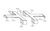
本実施形態においては、主ばねを構成しており、外部から印加される力に対して曲げ応力及び/又は捩り応力を発生させる第1の帯状板ばねが、2つに分割された第1の帯状板ばね171a1及び171a2から構成されている。さらに、第1の帯状板ばね171a1及び171a2の一端が支点を構成しており、この一端は一端が配線基板に固着されている支点部材176a及び176bの他端にそれぞれ固着されている。副ばねを構成しており、外部から印加される力に対して曲げ応力のみを発生させる2つの第2の帯状板ばね171b及び171cの中央部が第1の帯状板ばね171a1及び171a2の他端にそれぞれ一体的に連結されている。第2の帯状板ばね171b及び171cの両端部には、磁界発生錘部材22a、22b、22c′及び22d′が固着されている。さらに、本実施形態においては、磁界発生錘部材22a、22b、22c′及び22d′が第2の帯状板ばね21b及び21cの両端部に設けられた錘支持部の磁界検出センサチップ側の面上、即ち図2の実施形態とは反対側の面上、にそれぞれ固着されており、磁界発生錘部材22c′及び22d′の伸長方向が図2の実施形態の場合と異なっている。本実施形態のばね部材のように、主ばねが2分割されていても、図2の実施形態の場合と同様の機能を得ることができる。また、4つの磁界発生錘部材は、ばね部材のどちら側の面に取り付けても良い。さらに、第2の帯状板ばね171b及び171cの両端部にそれぞれ設けられる4つの磁界発生錘部材は方向、形状が互いに異なっていても重量的にバランスしていれば良い。
In the present embodiment, the first strip-shaped leaf spring that constitutes the main spring and generates bending stress and / or torsional stress with respect to externally applied force is divided into two. and a strip-shaped
本実施形態のばね部材及び磁界発生錘部材のその他の構成、さらに本実施形態の動作、作用効果等は図2の実施形態の場合と同様である。 Other configurations of the spring member and the magnetic field generating weight member of the present embodiment, and the operation, effects, and the like of the present embodiment are the same as those of the embodiment of FIG.
図18は本発明の加速度センサのさらに他の実施形態におけるばね部材及び磁界発生錘部材の構成を模式的に示す斜視図である。本実施形態におけるばね部材、磁界発生錘部材及び支点部材を除く構成は図2の実施形態の場合と同様である。従って、図18において、図2の実施形態と同じ構成要素については同じ参照番号を使用する。 FIG. 18 is a perspective view schematically showing a configuration of a spring member and a magnetic field generating weight member in still another embodiment of the acceleration sensor of the present invention. The configuration excluding the spring member, the magnetic field generating weight member, and the fulcrum member in this embodiment is the same as that in the embodiment of FIG. Accordingly, in FIG. 18, the same reference numerals are used for the same components as in the embodiment of FIG.
本実施形態においては、主ばねを構成しており、外部から印加される力に対して曲げ応力及び/又は捩り応力を発生させる第1の帯状板ばねが、2つに分割された第1の帯状板ばね171a1及び171a2から構成されている。さらに、第1の帯状板ばね171a1及び171a2の一端が支点を構成しており、この一端は一端が配線基板に固着されている支点部材176a及び176bの他端にそれぞれ固着されている。副ばねを構成しており、外部から印加される力に対して曲げ応力のみを発生させる2つの第2の帯状板ばね171b及び171cの中央部が第1の帯状板ばね171a1及び171a2の他端にそれぞれ一体的に連結されている。第2の帯状板ばね171b及び171cの両端部には、磁界発生錘部材22a、22b、22c′及び22d′が固着されている。さらに、本実施形態においては、磁界発生錘部材22a及び22c′並びに磁界発生錘部材22b及び22d′が剛性を有する帯状支持部材180a及び180bによってそれぞれ連結されており、磁界発生錘部材22c′及び22d′の伸長方向が図2の実施形態の場合と異なっている。本実施形態のばね部材のように、主ばねが2分割されていても、図2の実施形態の場合と同様の機能を得ることができる。また、帯状支持部材180a及び180bが固着されていることにより、第2の帯状板ばね171b及び171cはばね動作せず、第1の帯状板ばね171a1及び171a2のみがばね動作することになる。外部から印加される力に対して、第1の帯状板ばね171a1及び171a2は曲げ応力及び捩り応力を発生させ、磁界発生錘部材22a、22b、22c′及び22d′を変位させる。さらに、第2の帯状板ばね171b及び171cの両端部にそれぞれ設けられる4つの磁界発生錘部材は方向、形状が互いに異なっていても重量的にバランスしていれば良い。
In the present embodiment, the first strip-shaped leaf spring that constitutes the main spring and generates bending stress and / or torsional stress with respect to externally applied force is divided into two. and a strip-shaped
本実施形態のばね部材及び磁界発生錘部材のその他の構成、さらに本実施形態の動作、作用効果等は図2の実施形態の場合と同様である。 Other configurations of the spring member and the magnetic field generating weight member of the present embodiment, and the operation, effects, and the like of the present embodiment are the same as those of the embodiment of FIG.
図19は本発明の加速度センサのまたさらに他の実施形態における全体構成を概略的に示す分解斜視図であり、図20はハウジング部材の内部に設けられるばね部材、磁界発生錘部材及び磁界検出センサチップの構成を概略的に示す分解斜視図である。 FIG. 19 is an exploded perspective view schematically showing an overall configuration of still another embodiment of the acceleration sensor of the present invention, and FIG. 20 is a spring member provided inside the housing member, a magnetic field generating weight member, and a magnetic field detection sensor. It is a disassembled perspective view which shows the structure of a chip | tip schematically.
これらの図に示すように、本実施形態における加速度センサは、X軸方向及びZ軸方向又はY軸方向及びZ軸方向の2軸加速度を検出するためのものである。ただし、以下の説明では、X軸方向及びZ軸方向の2軸加速度を検出するためのものであるとする。 As shown in these drawings, the acceleration sensor in the present embodiment is for detecting biaxial acceleration in the X-axis direction and the Z-axis direction or the Y-axis direction and the Z-axis direction. However, in the following description, it is assumed to detect biaxial acceleration in the X-axis direction and the Z-axis direction.
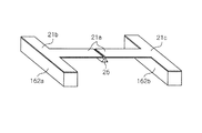
この加速度センサは、ハウジング部材190内に、帯状板ばね191a、及び磁界発生錘部材を支持するための2つの錘支持部191b及び191cを一体的に形成してなるばね部材191と、寸法、形状及び重量等の構成が同じである2つの磁界発生錘部材192a及び192bと、X軸Z軸用の第1の磁界検出センサチップ193と、X軸Z軸用の第2の磁界検出センサチップ194と、支点部材196とを収納するように構成されている。
This acceleration sensor includes a
ハウジング部材190は、基板自体が例えばポリイミド又はBTレジン等の樹脂材料による平板形状の基板に配線パターン(図示なし)を設けることで形成された配線基板190aと、この配線基板190aを覆って密封する磁性金属材料によって形成されたカバー部材190bとから構成されている。本実施形態では、X軸方向及びZ軸方向の2軸加速度を、配線基板190aによる1平面上に搭載した2つの磁界検出センサチップ193及び194で検出することが可能となる。
The
ばね部材21は、例えばNiFeやNi等による薄膜金属板か、ステンレス鋼等の薄板か、又はポリイミド等による薄い樹脂板を、本実施形態では、図20に示すように形状加工することによって一体的に形成されている。
In this embodiment, the
帯状板ばね191aは、外部から印加される力に対して曲げ応力を発生させる。この帯状板ばね191aの中央部は支点を構成しており、この中央部は一端がカバー部材190bに固着されている支点部材196の他端に固着されている。帯状板ばね191aの両端は互いに同一形状の錘支持部191b及び191cにそれぞれ一体的に連結されている。なお、錘支持部191b及び191cは図では矩形であるが、円形であってもその他の形状であっても良い。
The strip-shaped
磁界発生錘部材192a及び192bは、ばね部材191の錘支持部191b及び191cの一方の面上にそれぞれ接着剤で固着されている。磁界発生錘部材192a及び192bは、それぞれ、磁界発生用の1対の永久磁石192a1及び192a2並びに192b1及び192b2から構成されている。
The magnetic field generating
X軸Z軸用の第1の磁界検出センサチップ193及び第2の磁界検出センサチップ194は、2つの磁界発生錘部材192a及び192bにそれぞれ対向して、配線基板190a上に接着剤で固着されている。従って、磁界発生錘部材192a及び192bは、加速度に応じて角度の変化する磁界を第1及び第2の磁界検出センサチップ193及び194にそれぞれ印加することとなる。
The first magnetic field
1対の永久磁石192a1及び192a2は、X軸方向に互いに平行に伸長する直方体形状のフェライト材料で形成されており、X軸Z軸用の第1の磁界検出センサチップ193に対向している。これら1対の永久磁石192a1及び192a2は、第1の磁界検出センサチップ193に対向する面が互いに逆極性となるように配置されているおり、両者で閉磁路を構成している。後述するように、第1の磁界検出センサチップ193のスピンバルブGMR素子がこの閉磁路内にその積層面とほぼ垂直な方向に磁界(バイアス磁界)が印加されるように配置される。
The pair of
1対の永久磁石192b1及び192b2は、X軸方向に互いに平行に伸長する直方体形状のフェライト材料で形成されており、X軸Z軸用の第2の磁界検出センサチップ194に対向している。これら1対の永久磁石192b1及び192b2は、第2の磁界検出センサチップ194に対向する面が互いに逆極性となるように配置されているおり、両者で閉磁路を構成している。後述するように、第2の磁界検出センサチップ194のスピンバルブGMR素子がこの閉磁路内にその積層面とほぼ垂直な方向にバイアス磁界が印加されるように配置される。
The pair of
図21は本実施形態の加速度センサにおける配線基板上の結線及び磁界検出センサチップの構成を概略的に示す図であり、図22は本実施形態の加速度センサにおける配線基板及び磁界検出センサチップの電気的構成を概略的に示す回路図であり、図23は本実施形態の加速度センサにおける等価回路図である。 FIG. 21 is a diagram schematically showing the connection on the wiring board and the configuration of the magnetic field detection sensor chip in the acceleration sensor of the present embodiment, and FIG. 22 is an electrical diagram of the wiring board and magnetic field detection sensor chip in the acceleration sensor of the present embodiment. FIG. 23 is an equivalent circuit diagram of the acceleration sensor of the present embodiment.
これらの図に示すように、X軸Z軸方向の加速度を検出するための第1の磁界検出センサチップ193には、X軸方向と垂直な方向(Y軸方向)に沿った直線部分を有する4つ(2対)のスピンバルブGMR素子193a、193b、193c及び193dが互いに平行に形成されている。スピンバルブGMR素子193a及び193bは対となっており、互いに直列接続されている。その直列接続の両端が電源端子電極TVCC及びTVDDにそれぞれ接続されており、中点が信号出力端子TX1に接続されている。スピンバルブGMR素子193c及び193dも対となっており、互いに直列接続されている。その直列接続の両端が電源端子電極TVCC及びTVDDにそれぞれ接続されており、中点が信号出力端子TZ1に接続されている。
As shown in these drawings, the first magnetic field
スピンバルブGMR素子193a、193b、193c及び193dの各々は、基本的には、反強磁性材料によるピン層及び強磁性材料によるピンド層からなる磁化固定層と、非磁性中間層と、強磁性材料による磁化自由層(フリー層)とを積層した多層構造を有しており、ピンド層がフリー層の延在方向と垂直な同一方向に磁化固定されている。即ち、これらスピンバルブGMR素子193a、193b、193c及び193dのピンド層は、全てX軸方向の同一向きに磁化固定されている。
Each of the spin
互いに直列接続された対となるスピンバルブGMR素子193a及び193bのピンド層が同一方向に磁化固定されるのは、対となるスピンバルブGMR素子の各々に印加されるバイアス磁界が互いにほぼ逆方向であるためである。即ち、図22に示すように、1対の永久磁石192a1及び192a2によって閉磁路が構成されており、対となるスピンバルブGMR素子193a及び193bが、閉磁路の逆方向磁界が流れる磁路内に配置されているからバイアス磁界が互いにほぼ逆方向となるのである。互いに直列接続された対となるスピンバルブGMR素子193c及び193dについても同様である。この場合、閉磁路を構成する磁気回路の中心が、対となるスピンバルブGMR素子間の中心線上に位置していることとなる。
The pinned layers of the pair of spin
このように、互いにほぼ逆方向のバイアス磁界が印加されることにより、対をなすスピンバルブGMR素子193a及び193b並びに193c及び193dのピンド層の磁化固定方向が同一方向となるので、これら対をなす4つのスピンバルブGMR素子を1つのチップ内に形成することができ、その結果、加速度センサ全体のさらなる小型化を図ることが可能となる。
Thus, by applying bias magnetic fields in substantially opposite directions, the pinned layers of the spin
X軸Z軸方向の加速度を検出するための第2の磁界検出センサチップ194にも、X軸方向と垂直な方向(Y軸方向)に沿った直線部分を有する4つ(2対)のスピンバルブGMR素子194a、194b、194c及び194dが互いに平行に形成されている。スピンバルブGMR素子194b及び194aは対となっており、互いに直列接続されている。その直列接続の両端が電源端子電極TVCC及びTVDDにそれぞれ接続されており、中点が信号出力端子TX2接続されている。スピンバルブGMR素子194c及び194dも対となっており、互いに直列接続されている。その直列接続の両端が電源端子電極TVCC及びTVDDにそれぞれ接続されており、中点が信号出力端子TZ2接続されている。
The second magnetic field
スピンバルブGMR素子194a、194b、194c及び194dの各々は、基本的には、反強磁性材料によるピン層及び強磁性材料によるピンド層からなる磁化固定層と、非磁性中間層と、強磁性材料による磁化自由層(フリー層)とを積層した多層構造を有しており、ピンド層がフリー層の延在方向と垂直な同一方向に磁化固定されている。即ち、これらスピンバルブGMR素子194a、194b、194c及び194dのピンド層は、全てX軸方向の同一向きに磁化固定されている。
Each of the spin
互いに直列接続された対となるスピンバルブGMR素子194a及び194bのピンド層が同一方向に磁化固定されるのは、対となるスピンバルブGMR素子の各々に印加されるバイアス磁界が互いにほぼ逆方向であるためである。即ち、図22に示すように、1対の永久磁石192b1及び192b2によって閉磁路が構成されており、対となるスピンバルブGMR素子194a及び194bが、閉磁路の逆方向磁界が流れる磁路内に配置されているからバイアス磁界が互いにほぼ逆方向となるのである。互いに直列接続された対となるスピンバルブGMR素子194c及び194dについても同様である。この場合、閉磁路を構成する磁気回路の中心が、対となるスピンバルブGMR素子間の中心線上に位置していることとなる。
The pinned layers of the paired spin
このように、互いにほぼ逆方向のバイアス磁界が印加されることにより、対をなすスピンバルブGMR素子194a及び194b並びに194c及び194dのピンド層の磁化固定方向が同一方向となるので、これら対をなす4つのスピンバルブGMR素子を1つのチップ内に形成することができ、その結果、加速度センサ全体のさらなる小型化を図ることが可能となる。
Thus, by applying bias magnetic fields in substantially opposite directions, the pinned layers of the spin
第1の磁界検出センサチップ193のスピンバルブGMR素子193a及び193b間には電源電圧Vcc−Vddが印加され、その中点に接続された信号出力端子TX1から第1のX軸方向加速度信号VX1が取り出される。また、第2の磁界検出センサチップ194のスピンバルブGMR素子194b及び194a間には電源電圧Vcc−Vddが印加され、その中点に接続された信号出力端子TX2から第2のX軸方向加速度信号VX2が取り出される。従って、これらスピンバルブGMR素子193a及び193b並びに194b及び194aは、図23(A)に示すようにフルブリッジ接続されていることとなり、信号出力端子TX1及び信号出力端子TX2からの信号VX1及びVX2が差動増幅されてX軸方向の加速度信号となる。このX軸方向の加速度信号は、印加される加速度の方向によって、磁界発生錘部材192a(従って永久磁石192a1及び192a2)と磁界発生錘部材192b(従って永久磁石192b1及び192b2)とがZ軸の互いに反対方向に変位した際にのみ出力され、共に同じ方向に変位した際には第1のX軸方向加速度信号VX1及び第2のX軸方向加速度信号VX2が互いに打ち消し合って出力されない。
A power supply voltage Vcc-Vdd is applied between the spin
第1の磁界検出センサチップ193のスピンバルブGMR素子193c及び193d間には電源電圧Vcc−Vddが印加され、その中点に接続された信号出力端子TZ1から第1のZ軸方向加速度信号VZ1が取り出される。また、第2の磁界検出センサチップ194のスピンバルブGMR素子194c及び194d間には電源電圧Vcc−Vddが印加され、その中点に接続された信号出力端子TZ2から第2のZ軸方向加速度信号VZ2が取り出される。従って、これらスピンバルブGMR素子193c及び193d並びに194c及び194dは、図23(B)に示すようにフルブリッジ接続されていることとなり、信号出力端子TZ1及び信号出力端子TZ2からの信号VZ1及びVZ2が差動増幅されてZ軸方向の加速度信号となる。このZ軸方向の加速度信号は、印加される加速度によって、磁界発生錘部材192a(従って永久磁石192a1及び192a2)と磁界発生錘部材192b(従って永久磁石192b1及び192b2)とがZ軸の共に同じ方向に変位した際にのみ出力され、互いに反対方向に変位した際には第1のZ軸方向加速度信号VZ1及び第2のZ軸方向加速度信号VZ2が互いに打ち消し合って出力されない。
The first power supply voltage Vcc-Vdd is applied across the spin
次に、本実施形態におけるばね部材191についてより詳細に説明する。
Next, the
図24は本実施形態におけるばね部材の動作を説明するための図である。 FIG. 24 is a view for explaining the operation of the spring member in the present embodiment.
同図(A)は外力が印加されていない場合であり、変位は発生しない。一方、同図(B)に示すようにX軸方向に外力Fxが印加されると、帯状板ばね191aは曲げ応力を発生させ、平衡が保たれる位置まで曲げ方向に変位する。この場合、帯状板ばね191aの両端部及び磁界発生錘部材192a及び192bの変位方向は互いに逆方向である。また、同図(C)に示すようにZ軸方向に外力Fzが印加されると、帯状板ばね191aは曲げ応力を発生させ、平衡が保たれる位置まで曲げ方向に変位する。この場合、帯状板ばね191aの両端部及び磁界発生錘部材192a及び192bの変位方向は共に同じ方向である。磁界発生錘部材192a及び192bの変位量は、それらの変位角に比例する。磁界発生錘部材の角度がこのように変化すると、スピンバルブGMR素子は、その変位角を検出して印加される外力を検出することができる。外力Fxが印加された際の磁界発生錘部材192a及び192bの変位角をそれぞれθX1及びθX2とすると、Fx=θX1−θX2で与えられる。また、外力Fzが印加された際の磁界発生錘部材192a及び192bの変位角をそれぞれθZ1及びθZ2とすると、Fz=θZ1+θZ2で与えられる。
FIG. 6A shows a case where no external force is applied, and no displacement occurs. On the other hand, when an external force Fx is applied in the X-axis direction as shown in FIG. 5B, the strip-shaped
X軸方向の外力Fxが印加され、磁界発生錘部材192a及び192bが上述のごとく曲げ方向に変位すると、スピンバルブGMR素子193a及び193b並びに194b及び194aに印加されるバイアス磁界の角度がこれに伴って同じ方向に変化し、第1のX軸方向加速度信号VX1及び第2のX軸方向加速度信号VX2を加算した差動出力が得られ、これがX軸方向の加速度信号となる。この場合、第1のZ軸方向加速度信号VZ1及び第2のZ軸方向加速度信号VZ2が互いに打ち消し合い、Z軸方向の加速度信号は出力されない。
When the external force Fx in the X-axis direction is applied and the magnetic field generating
Z軸方向の外力Fzが印加され、磁界発生錘部材192a及び192bが上述のごとく曲げ方向に変位すると、スピンバルブGMR素子193c及び193d並びに194c及び194dに印加されるバイアス磁界の角度がこれに伴って反対方向に変化し、第1のZ軸方向加速度信号VZ1及び第2のZ軸方向加速度信号VZ2を加算した差動出力が得られ、これがZ軸方向の加速度信号となる。この場合、第1のX軸方向加速度信号VX1及び第2のX軸方向加速度信号VX2が互いに打ち消し合い、X軸方向の加速度信号は出力されない。
When the external force Fz in the Z-axis direction is applied and the magnetic field generating
以上説明したように、本実施形態によれば、帯状板ばね191aが曲げ応力を発生させ、平衡が保たれる位置まで変位するように構成されているため、小型でかつ変位量が大きい、従って小型で感度の高いばね構造とすることができ、小型かつ高感度の加速度センサを提供することができる。
As described above, according to the present embodiment, the strip-shaped
ばね部材の2つの端部の構造を同一形状とすることができるため、検出したい各方向(X軸方向及びZ軸方向、又はY軸方向及びZ軸方向)の感度、感度指向性が揃った加速度センサを提供することができる。 Since the two ends of the spring member can have the same shape, the sensitivity and sensitivity directivity in each direction (X-axis direction and Z-axis direction, or Y-axis direction and Z-axis direction) to be detected are aligned. An acceleration sensor can be provided.
さらに、本実施形態によれば、中央に支点を有し両端部に磁界発生錘部材をそれぞれ固着した帯状板ばね191aの曲げ動作を利用すると共に、第1の磁界検出センサチップ193の一部出力VX1又はVZ1と第2の磁界検出センサチップ194の一部出力VX2又はVZ2との差動出力を取り出すようにしているので、X軸方向及びZ軸方向の加速度成分を確実に分離して正確に検出することができる。
Further, according to the present embodiment, the bending operation of the strip-shaped
また、2軸方向の加速度の向き及び大きさを2つの磁界検出センサチップで検出できるので、磁界検出センサチップ数が低減でき構造を非常に簡単化でき、加速度センサ全体を小型化することができる。また、スピンバルブGMR素子は磁気検出感度が非常に高いので、高感度の加速度検出を行なうことが可能となる。 In addition, since the direction and magnitude of the acceleration in the biaxial direction can be detected by two magnetic field detection sensor chips, the number of magnetic field detection sensor chips can be reduced, the structure can be greatly simplified, and the entire acceleration sensor can be reduced in size. . In addition, since the spin valve GMR element has a very high magnetic detection sensitivity, it is possible to detect acceleration with high sensitivity.
さらにまた、各磁界検出センサチップにおいて、互いにほぼ逆方向のバイアス磁界が印加されるため、対をなすスピンバルブGMR素子のピンド層の磁化固定方向が同一方向となりこれら対をなす4つのスピンバルブGMR素子を1つのチップ内に形成することができる。その結果、加速度センサ全体のさらなる小型化を図ることが可能となる。 Furthermore, in each magnetic field detection sensor chip, bias magnetic fields in opposite directions are applied to each other, so that the pinned layers of the paired spin valve GMR elements have the same magnetization fixed direction, and the four spin valves GMR that form these pairs. Elements can be formed in one chip. As a result, the entire acceleration sensor can be further reduced in size.
さらに、本実施形態によれば、対となる2つの永久磁石によって、広い範囲に分布した垂直方向の磁界による閉磁路が形成され、スピンバルブGMR素子がこの閉磁路中に配置されるため、必要最小限の磁界しか閉磁路から外部へ漏れず、漏れ磁界が少なくなるから充分に大きなバイアス磁界が印加されることとなり、永久磁石が小型となった場合にも、加速度の検出感度が安定してかつ高くなり、しかも外部電界及び外部磁界の影響を受けにくくなる。 Further, according to the present embodiment, a closed magnetic circuit is formed by a vertical magnetic field distributed over a wide range by two pairs of permanent magnets, and the spin valve GMR element is disposed in this closed magnetic circuit. Only a minimum magnetic field leaks from the closed magnetic circuit to the outside, and since the leakage magnetic field is reduced, a sufficiently large bias magnetic field is applied. Even when the permanent magnet is downsized, the detection sensitivity of acceleration is stable. In addition, it becomes high and is hardly affected by an external electric field and an external magnetic field.
本実施形態によれば、さらに、ばね部材や磁界発生錘部材の部分に電極を設ける必要がないため、配線構造が簡単となる。また、圧電素子型加速度センサや静電容量型加速度センサに比して低インピーダンスであるため、外乱の影響も受けにくい。 Further, according to the present embodiment, since it is not necessary to provide an electrode on the spring member or the magnetic field generating weight member, the wiring structure is simplified. Further, since it has a lower impedance than a piezoelectric element type acceleration sensor or a capacitance type acceleration sensor, it is not easily affected by disturbances.
なお、上述の実施形態では、閉磁路を形成するために磁界検出センサチップに対向する面が互いに逆極性となるように配置された2つの永久磁石を用いているが、1つの永久磁石と例えば軟磁性体からなるヨークとを組み合わせても閉磁路を形成することは可能である。 In the above-described embodiment, in order to form a closed magnetic circuit, two permanent magnets arranged so that the surfaces facing the magnetic field detection sensor chip have opposite polarities are used. Even when combined with a yoke made of a soft magnetic material, a closed magnetic circuit can be formed.
上述した実施形態では、磁界検出センサとしてスピンバルブGMR素子を用いているが、その代わりにTMR素子を用いても良いことは明らかである。 In the above-described embodiment, the spin valve GMR element is used as the magnetic field detection sensor, but it is obvious that a TMR element may be used instead.
なお、本発明の加速度センサが、上述した実施形態のごとく磁気ディスクドライブ装置のみに適用されるものではなく、加速度を検出するいかなる用途にも適用可能であることはいうまでもない。 Needless to say, the acceleration sensor of the present invention is not only applied to the magnetic disk drive device as in the above-described embodiment, but can be applied to any application for detecting acceleration.
以上述べた実施形態は全て本発明を例示的に示すものであって限定的に示すものではなく、本発明は他の種々の変形態様及び変更態様で実施することができる。従って本発明の範囲は特許請求の範囲及びその均等範囲によってのみ規定されるものである。 All the embodiments described above are illustrative of the present invention and are not intended to be limiting, and the present invention can be implemented in other various modifications and changes. Therefore, the scope of the present invention is defined only by the claims and their equivalents.
10 磁気ディスク
10a 退避ゾーン
11 HGA
12 FPC
13 支持アーム
13a 爪
14 VCM
15 回動軸
16 退避ランプ
17 加速度センサ
18 回路基板
20、190 ハウジング部材
20a、190a 配線基板
20b、190b カバー部材
21、191 ばね部材
21a、171a1、171a2、 第1の帯状板ばね
21b、21c、171b、171c 第2の帯状板ばね
21d、21e、21f、21g、191b、191c 錘支持部
22a、22b、22c、22c′、22d、22d′、162a、162b、192a、192b 磁界発生錘部材
22a1、22a2、22b1、22b2、22c1、22c2、22d1、22d2、192a1、192a2、192b1、192b2 永久磁石
23、24、25、193、194 磁界検出センサチップ
23a、23b、23c、23d、24a、24b、24c、24d、25a、25b、25c、25d、193a、193b、193c、193d、194a、194b、194c、194d スピンバルブGMR素子
26、176a、176b、196 支点部材
80、90、191a 帯状板ばね
81、91 支点
82、92a、92b 錘部材
130a、130b、180a、180b 帯状支持部材
10
12 FPC
13
15
Claims (7)
Priority Applications (5)
| Application Number | Priority Date | Filing Date | Title |
|---|---|---|---|
| JP2005338328A JP4367403B2 (en) | 2005-11-24 | 2005-11-24 | Spring member for acceleration sensor, acceleration sensor, and magnetic disk drive device |
| US11/549,820 US7543498B2 (en) | 2005-11-24 | 2006-10-16 | Spring member for acceleration sensor, acceleration sensor and magnetic disk drive apparatus |
| EP06124691A EP1790986B1 (en) | 2005-11-24 | 2006-11-23 | Spring member for acceleration sensor, acceleration sensor and magnetic disk drive apparatus |
| DE602006019538T DE602006019538D1 (en) | 2005-11-24 | 2006-11-23 | Spring element for accelerometer, accelerometer and magnetic disk drive device |
| CN200610145373A CN100578230C (en) | 2005-11-24 | 2006-11-24 | Spring member for acceleration sensor, acceleration sensor and magnetic disk drive apparatus |
Applications Claiming Priority (1)
| Application Number | Priority Date | Filing Date | Title |
|---|---|---|---|
| JP2005338328A JP4367403B2 (en) | 2005-11-24 | 2005-11-24 | Spring member for acceleration sensor, acceleration sensor, and magnetic disk drive device |
Publications (2)
| Publication Number | Publication Date |
|---|---|
| JP2007147303A JP2007147303A (en) | 2007-06-14 |
| JP4367403B2 true JP4367403B2 (en) | 2009-11-18 |
Family
ID=37744595
Family Applications (1)
| Application Number | Title | Priority Date | Filing Date |
|---|---|---|---|
| JP2005338328A Expired - Fee Related JP4367403B2 (en) | 2005-11-24 | 2005-11-24 | Spring member for acceleration sensor, acceleration sensor, and magnetic disk drive device |
Country Status (5)
| Country | Link |
|---|---|
| US (1) | US7543498B2 (en) |
| EP (1) | EP1790986B1 (en) |
| JP (1) | JP4367403B2 (en) |
| CN (1) | CN100578230C (en) |
| DE (1) | DE602006019538D1 (en) |
Families Citing this family (4)
| Publication number | Priority date | Publication date | Assignee | Title |
|---|---|---|---|---|
| JP2007033045A (en) * | 2005-07-22 | 2007-02-08 | Tdk Corp | Spring member for acceleration sensor, acceleration sensor and magnetic disk drive device |
| JP4222375B2 (en) * | 2006-02-09 | 2009-02-12 | Tdk株式会社 | Acceleration sensor and magnetic disk drive device |
| CN101752974B (en) * | 2008-12-02 | 2012-12-19 | 鸿富锦精密工业(深圳)有限公司 | Flat spring plate |
| US10180445B2 (en) * | 2016-06-08 | 2019-01-15 | Honeywell International Inc. | Reducing bias in an accelerometer via current adjustment |
Family Cites Families (19)
| Publication number | Priority date | Publication date | Assignee | Title |
|---|---|---|---|---|
| DE3538766A1 (en) * | 1985-10-31 | 1987-05-07 | Bosch Gmbh Robert | ACCELERATOR |
| DE3638360A1 (en) * | 1986-11-10 | 1988-05-19 | Boge Ag | Accelerometer |
| DE3929082A1 (en) * | 1988-12-09 | 1990-06-13 | Teves Gmbh Alfred | ACCELERATION SENSOR WITH SINGLE-SIDED CLAMP |
| JP2732287B2 (en) | 1989-03-23 | 1998-03-25 | 東洋通信機株式会社 | Acceleration sensor |
| JPH0325162A (en) | 1989-06-21 | 1991-02-01 | Taisei Corp | Concrete plate placing method and device |
| DE9109579U1 (en) * | 1991-08-02 | 1992-12-03 | Robert Bosch Gmbh, 7000 Stuttgart, De | |
| JP2586406B2 (en) | 1994-10-27 | 1997-02-26 | 日本電気株式会社 | Capacitive acceleration sensor |
| JPH11352143A (en) | 1998-04-06 | 1999-12-24 | Matsushita Electric Ind Co Ltd | Acceleration sensor |
| GB2343952B (en) * | 1998-11-18 | 2000-11-08 | Breed Automotive Tech | Pendulum mass acceleration sensor |
| JP2002100180A (en) * | 2000-09-22 | 2002-04-05 | Toshiba Corp | Magnetic disk unit |
| FR2861464B1 (en) | 2003-10-28 | 2006-02-17 | Commissariat Energie Atomique | MOTION DETECTOR WITH SIX DEGREES OF FREEDOM WITH THREE POSITION SENSORS AND METHOD OF MANUFACTURING A SENSOR |
| JP2005291746A (en) | 2004-03-31 | 2005-10-20 | Tdk Corp | Inertia sensor |
| KR100632458B1 (en) * | 2004-04-30 | 2006-10-11 | 아이치 세이코우 가부시키가이샤 | Accelerometer |
| JP4261468B2 (en) | 2004-11-18 | 2009-04-30 | Tdk株式会社 | Acceleration sensor |
| JP4229096B2 (en) * | 2005-07-21 | 2009-02-25 | Tdk株式会社 | Acceleration sensor and magnetic disk drive device |
| JP4460509B2 (en) | 2005-08-31 | 2010-05-12 | 新科實業有限公司 | Acceleration sensor and electronic device equipped with the same |
| JP2007147304A (en) * | 2005-11-24 | 2007-06-14 | Tdk Corp | Acceleration sensor and magnetic disk drive device |
| JP4222375B2 (en) * | 2006-02-09 | 2009-02-12 | Tdk株式会社 | Acceleration sensor and magnetic disk drive device |
| JP4285488B2 (en) * | 2006-02-16 | 2009-06-24 | Tdk株式会社 | Acceleration sensor and magnetic disk drive device |
-
2005
- 2005-11-24 JP JP2005338328A patent/JP4367403B2/en not_active Expired - Fee Related
-
2006
- 2006-10-16 US US11/549,820 patent/US7543498B2/en not_active Expired - Fee Related
- 2006-11-23 EP EP06124691A patent/EP1790986B1/en not_active Expired - Fee Related
- 2006-11-23 DE DE602006019538T patent/DE602006019538D1/en active Active
- 2006-11-24 CN CN200610145373A patent/CN100578230C/en not_active Expired - Fee Related
Also Published As
| Publication number | Publication date |
|---|---|
| CN100578230C (en) | 2010-01-06 |
| US7543498B2 (en) | 2009-06-09 |
| CN1971283A (en) | 2007-05-30 |
| EP1790986A2 (en) | 2007-05-30 |
| DE602006019538D1 (en) | 2011-02-24 |
| US20070119253A1 (en) | 2007-05-31 |
| JP2007147303A (en) | 2007-06-14 |
| EP1790986A3 (en) | 2010-01-06 |
| EP1790986B1 (en) | 2011-01-12 |
Similar Documents
| Publication | Publication Date | Title |
|---|---|---|
| JP4222375B2 (en) | Acceleration sensor and magnetic disk drive device | |
| JP4229096B2 (en) | Acceleration sensor and magnetic disk drive device | |
| JP2007147304A (en) | Acceleration sensor and magnetic disk drive device | |
| US7222535B2 (en) | Acceleration sensor and magnetic disk drive apparatus | |
| JP4285488B2 (en) | Acceleration sensor and magnetic disk drive device | |
| JP2008515043A (en) | Magnetic sensor for input device | |
| JP4367403B2 (en) | Spring member for acceleration sensor, acceleration sensor, and magnetic disk drive device | |
| US7679865B2 (en) | Spring member for acceleration sensor, acceleration sensor and magnetic disk drive apparatus | |
| US7403352B2 (en) | Acceleration sensor and magnetic disk drive apparatus | |
| JP4556933B2 (en) | Acceleration sensor and magnetic disk drive device | |
| JP2009266348A (en) | Head suspension and disk device | |
| JP2005337992A (en) | Inertial sensor and disc record reproducing device having the same | |
| JP2005114641A (en) | Acceleration sensor | |
| JP4404364B2 (en) | Compact acceleration geomagnetic detector using magnetic acceleration sensor | |
| JP2005069963A (en) | Acceleration sensor | |
| JP2005201699A (en) | Inertia sensor |
Legal Events
| Date | Code | Title | Description |
|---|---|---|---|
| A977 | Report on retrieval |
Free format text: JAPANESE INTERMEDIATE CODE: A971007 Effective date: 20080811 |
|
| A131 | Notification of reasons for refusal |
Free format text: JAPANESE INTERMEDIATE CODE: A131 Effective date: 20081202 |
|
| A521 | Written amendment |
Free format text: JAPANESE INTERMEDIATE CODE: A523 Effective date: 20081224 |
|
| A131 | Notification of reasons for refusal |
Free format text: JAPANESE INTERMEDIATE CODE: A131 Effective date: 20090303 |
|
| A521 | Written amendment |
Free format text: JAPANESE INTERMEDIATE CODE: A523 Effective date: 20090310 |
|
| TRDD | Decision of grant or rejection written | ||
| A01 | Written decision to grant a patent or to grant a registration (utility model) |
Free format text: JAPANESE INTERMEDIATE CODE: A01 Effective date: 20090804 |
|
| A01 | Written decision to grant a patent or to grant a registration (utility model) |
Free format text: JAPANESE INTERMEDIATE CODE: A01 |
|
| A61 | First payment of annual fees (during grant procedure) |
Free format text: JAPANESE INTERMEDIATE CODE: A61 Effective date: 20090817 |
|
| R150 | Certificate of patent or registration of utility model |
Free format text: JAPANESE INTERMEDIATE CODE: R150 |
|
| FPAY | Renewal fee payment (event date is renewal date of database) |
Free format text: PAYMENT UNTIL: 20120904 Year of fee payment: 3 |
|
| LAPS | Cancellation because of no payment of annual fees |