JP4367100B2 - Image display device - Google Patents
Image display device Download PDFInfo
- Publication number
- JP4367100B2 JP4367100B2 JP2003387660A JP2003387660A JP4367100B2 JP 4367100 B2 JP4367100 B2 JP 4367100B2 JP 2003387660 A JP2003387660 A JP 2003387660A JP 2003387660 A JP2003387660 A JP 2003387660A JP 4367100 B2 JP4367100 B2 JP 4367100B2
- Authority
- JP
- Japan
- Prior art keywords
- circuit
- image
- frame
- video signal
- image data
- Prior art date
- Legal status (The legal status is an assumption and is not a legal conclusion. Google has not performed a legal analysis and makes no representation as to the accuracy of the status listed.)
- Expired - Lifetime
Links
- 238000006243 chemical reaction Methods 0.000 claims description 56
- 230000015654 memory Effects 0.000 claims description 45
- 239000013598 vector Substances 0.000 claims description 40
- 239000011159 matrix material Substances 0.000 claims description 17
- 238000001514 detection method Methods 0.000 claims description 16
- 238000010586 diagram Methods 0.000 description 19
- 239000004973 liquid crystal related substance Substances 0.000 description 19
- 238000005070 sampling Methods 0.000 description 11
- 230000000694 effects Effects 0.000 description 9
- 230000004044 response Effects 0.000 description 9
- 238000000034 method Methods 0.000 description 8
- 230000003111 delayed effect Effects 0.000 description 7
- 230000010354 integration Effects 0.000 description 4
- 230000000007 visual effect Effects 0.000 description 4
- 206010047571 Visual impairment Diseases 0.000 description 3
- 230000008901 benefit Effects 0.000 description 3
- 238000009416 shuttering Methods 0.000 description 3
- 238000007796 conventional method Methods 0.000 description 2
- 230000006872 improvement Effects 0.000 description 2
- 230000004298 light response Effects 0.000 description 2
- 238000013459 approach Methods 0.000 description 1
- 239000003990 capacitor Substances 0.000 description 1
- 230000015556 catabolic process Effects 0.000 description 1
- 230000007423 decrease Effects 0.000 description 1
- 238000006731 degradation reaction Methods 0.000 description 1
- 230000003292 diminished effect Effects 0.000 description 1
- 238000002474 experimental method Methods 0.000 description 1
- 230000001771 impaired effect Effects 0.000 description 1
- 230000006386 memory function Effects 0.000 description 1
- 230000000750 progressive effect Effects 0.000 description 1
- 230000009467 reduction Effects 0.000 description 1
- 239000010409 thin film Substances 0.000 description 1
Images


Landscapes
- Liquid Crystal (AREA)
- Liquid Crystal Display Device Control (AREA)
- Transforming Electric Information Into Light Information (AREA)
- Television Systems (AREA)
- Control Of Indicators Other Than Cathode Ray Tubes (AREA)
Description
本発明は、液晶表示装置に代表されるホールド型の画像表示装置に係り、動画像のぼやけ感を低減することができる画像表示装置に関する。 The present invention relates to a hold-type image display device typified by a liquid crystal display device, and more particularly to an image display device that can reduce the blur of moving images.
画像表示装置には、陰極線管(CRT)を用いた表示装置のように画像の書き込みの瞬間に強く発光するインパルス型表示装置と、各画素毎にメモリ機能を持ったアクティブマトリクス型表示装置のように画像が書き込まれてから次のフレームの画像が書き込まれるまで表示を保持しているホールド型表示装置とがある。アクティブマトリクス型表示装置としては、薄膜トランジスタ(TFT)を用いた液晶表示装置がある。液晶表示装置では、画素毎に配置されたTFTとコンデンサとによって画素に書き込まれた画像を一定時間保持する。
液晶表示装置は応答速度が遅いため、動画を表示したときに残像を生じるという問題点がある。この問題点を低減する方法の1つとして、映像信号を時間軸方向に強調するフィルタ(時間軸強調回路)を用いる方法がある。
The image display device includes an impulse display device that emits light strongly at the moment of image writing, such as a display device using a cathode ray tube (CRT), and an active matrix display device that has a memory function for each pixel. There is a hold-type display device that holds a display until an image of the next frame is written after an image is written. As an active matrix display device, there is a liquid crystal display device using a thin film transistor (TFT). In a liquid crystal display device, an image written in a pixel is held for a certain time by a TFT and a capacitor arranged for each pixel.
Since the liquid crystal display device has a low response speed, there is a problem that an afterimage is generated when a moving image is displayed. One method of reducing this problem is to use a filter (time axis enhancement circuit) that enhances the video signal in the time axis direction.
ところが、液晶表示装置のようなホールド型表示装置においては、液晶の応答速度をいくら高速にしてもホールド表示そのものに起因する視覚系積分の影響による動画像のぼやけ感(以下、動画ぼやけ)を解決することはできない。
この問題点及びその解決策は下記の非特許文献1に記載されている。なお、動画ぼやけは液晶表示装置のみならず、有機エレクトロルミネセンス表示装置であってもアクティブマトリクス型の場合には同様に発生する。非特許文献1には動画ぼやけの解決策として、ホールド時間を短くしてインパルス型の表示に近づける第1の方法と、フレーム周波数が60Hzである入力映像信号のフレーム周波数を動き補償手段によって2倍の120Hzに高速化する第2の方法とが記載されている。
This problem and its solution are described in Non-Patent
上記の第1の方法においては、映像信号と同期させてバックライトをシャッタする手段が必要となると共に、ホールド型表示の利点であるちらつきのない表示が損なわれてしまうという欠点(第1の問題点)がある。上記の第2の方法においては、フレーム周波数を2倍に上げるために、映像信号のサンプリング周波数及び液晶の書き込み速度をそれぞれ2倍にしなければならず、回路の動作速度や回路間の接続インターフェースにとって大きな負担となり、実現上の困難さを伴うという欠点(第2の問題点)がある。 The first method requires a means for shuttering the backlight in synchronism with the video signal, and has the disadvantage that the flicker-free display that is an advantage of the hold-type display is impaired (first problem). Point). In the second method, in order to double the frame frequency, the sampling frequency of the video signal and the writing speed of the liquid crystal must be doubled, respectively, for the circuit operation speed and the connection interface between the circuits. There is a drawback (second problem) that it is a heavy burden and is difficult to implement.
本発明はこのような問題点に鑑みなされたものであり、ちらつきのない表示を行うことができるというホールド型表示の利点を損なうことなく、動画ぼやけを低減することができる画像表示装置を提供することを目的とする。また、動画ぼやけを低減するに際し、回路の動作速度や回路間の接続インターフェースにとっての負担が少なく実現が容易な画像表示装置を提供することを目的とする。 The present invention has been made in view of such a problem, and provides an image display device capable of reducing moving image blurring without impairing the advantage of hold-type display that can perform display without flickering. For the purpose. It is another object of the present invention to provide an image display device that can be easily realized with less burden on the operation speed of the circuit and the connection interface between the circuits when reducing the motion blur.
本発明は、上述した従来の技術の課題を解決するため、マトリクス状に配列された複数の画素を有し、電気信号を画素毎に所定時間保持して表示するアクティブマトリクス型表示パネルを用いた画像表示装置において、第1の垂直周波数を有する映像信号を、前記第1の垂直周波数のm/n倍(ここで、mは2以上の整数、nは1以上の整数であり、m>nという条件を満たす)である第2の垂直周波数に変換して出力するレート変換回路(10’)と、前記レート変換回路より出力された前記第2の垂直周波数を有する映像信号における隣接する2フレーム分の画像データを用いて時間軸方向の高域成分を強調する時間軸強調回路(20’)と、前記時間軸強調回路より出力された前記第2の垂直周波数を有する映像信号を前記アクティブマトリクス型表示パネルに表示する駆動回路(30)とを備え、前記レート変換回路は、前記第1の垂直周波数を有する映像信号を書き込んで前記第2の垂直周波数の映像信号として出力する複数の画像メモリ(101,102)と、前記複数の画像メモリより出力された画像データを用いて動きベクトルを検出する動きベクトル検出回路(103)と、前記複数の画像メモリより出力された画像データと前記動きベクトルとを用いて動き補償補間して、前記第2の垂直周波数の映像信号であり互いに1フレーム分ずれた関係にある画像データを出力する第1及び第2の内挿回路(1041,1042)とを備え、前記時間軸強調回路は、前記隣接する2フレーム分の画像データとして前記第1及び第2の内挿回路より出力された画像データを用いて時間軸方向の高域成分を強調することを特徴とする画像表示装置を提供する。 The present invention for solving the problems of the prior art described above, a plurality of pixels arranged in a matrix, use the electrical signal to the image Motogoto an active matrix type display panel that displays holding a predetermined time In the image display apparatus, a video signal having a first vertical frequency is converted to m / n times the first vertical frequency (where m is an integer of 2 or more, n is an integer of 1 or more, m> a rate conversion circuit ( 10 ′ ) that converts and outputs a second vertical frequency that satisfies the condition of n) and two adjacent video signals having the second vertical frequency that are output from the rate conversion circuit. a frame image data to emphasize the time axis emphasizing circuit the high-frequency component in the time axis direction using the (20 '), the active video signal having the second vertical frequency output from the time axis emphasis circuit And a drive circuit for displaying on Torikusu display panel (30), said rate conversion circuit includes a plurality of images to be output as a video signal of said second vertical frequency by writing a video signal having a first vertical frequency A memory (101, 102), a motion vector detection circuit (103) for detecting a motion vector using the image data output from the plurality of image memories, the image data output from the plurality of image memories and the motion First and second interpolation circuits (1041, 1042) that output image data that is a video signal having the second vertical frequency and is shifted by one frame from each other by performing motion compensation interpolation using a vector. And the time axis emphasizing circuit uses the image data output from the first and second interpolation circuits as the image data for the two adjacent frames. An image display device characterized by emphasizing high-frequency components in the axial direction is provided.
さらに、本発明は、上述した従来の技術の課題を解決するため、本発明は、上述した従来の技術の課題を解決するため、マトリクス状に配列された複数の画素を有し、電気信号を画素毎に所定時間保持して表示するアクティブマトリクス型表示パネルを用いた画像表示装置において、第1の垂直周波数を有する映像信号を、前記第1の垂直周波数のm/n倍(ここで、mは2以上の整数、nは1以上の整数であり、m>nという条件を満たす)である第2の垂直周波数に変換して出力するレート変換回路(10”)と、前記レート変換回路より出力された前記第2の垂直周波数を有する映像信号における隣接する2フレーム分の画像データを用いて時間軸方向の高域成分を強調する時間軸強調回路(20’)と、前記時間軸強調回路より出力された前記第2の垂直周波数を有する映像信号を前記アクティブマトリクス型表示パネルに表示する駆動回路(30)とを備え、前記レート変換回路は、前記第1の垂直周波数を有する映像信号を書き込んで前記第2の垂直周波数の映像信号として出力する複数の画像メモリ(101,102)と、前記複数の画像メモリより出力された画像データを用いて動きベクトルを検出する動きベクトル検出回路(103)と、前記複数の画像メモリより出力された画像データと前記動きベクトルとを用いて動き補償補間して、前記第2の垂直周波数の映像信号を出力する内挿回路(104)と、前記複数の画像メモリより出力された画像データと前記内挿回路より出力された画像データとを選択的に出力することにより互いに1フレーム分ずれた関係にある画像データを出力する第1及び第2のセレクタ(1051,1052)とを有し、前記時間軸強調回路は、前記隣接する2フレーム分の画像データとして前記第1及び第2のセレクタより出力された画像データを用いて時間軸方向の高域成分を強調することを特徴とする画像表示装置を提供する。
Furthermore, the present invention solves the above-described problems of the conventional technique, and the present invention solves the problems of the above-described conventional technique, and has a plurality of pixels arranged in a matrix and outputs an electric signal . in the image display device using an active matrix type display panel for displaying to hold a predetermined time image Motogoto, a video signal having a first vertical frequency, the first m / n times (where the vertical frequency, m is an integer greater than or equal to 2, n is an integer greater than or equal to 1, and the rate conversion circuit (10 ″) for converting to a second vertical frequency and satisfying the condition that m> n) and the rate conversion circuit A time axis emphasizing circuit (20 ′) for emphasizing a high frequency component in the time axis direction using image data for two adjacent frames in the video signal having the second vertical frequency outputted from the time axis, and the time axis emphasis Output from circuit And a drive circuit (30) for displaying the video signal having the second vertical frequency on the active matrix display panel, and the rate conversion circuit writes the video signal having the first vertical frequency. A plurality of image memories (101, 102) that output as video signals of the second vertical frequency, and a motion vector detection circuit (103) that detects a motion vector using image data output from the plurality of image memories; An interpolation circuit (104) for performing motion compensation interpolation using the image data output from the plurality of image memories and the motion vector, and outputting the video signal of the second vertical frequency, and the plurality of images The image data output from the memory and the image data output from the interpolation circuit are selectively output so that they are shifted from each other by one frame. First and second selectors (1051, 1052) for outputting certain image data, and the time axis emphasizing circuit outputs the image data for the two adjacent frames from the first and second selectors. There is provided an image display device characterized by emphasizing a high frequency component in a time axis direction using the image data thus obtained.
本発明によれば、ちらつきのない表示を行うことができるというホールド型表示の利点を損なうことなく、動画ぼやけを低減することができる。本発明は、回路の動作速度や回路間の接続インターフェースにとっての負担が少なく容易に実現可能である。また、バックライトをシャッタする等の特別な回路を必要としないので、コストアップも少ない。 According to the present invention, it is possible to reduce moving image blurring without impairing the advantage of hold-type display that can perform display without flicker. The present invention can be easily realized with less burden on the operation speed of the circuit and the connection interface between the circuits. Further, since a special circuit such as shuttering the backlight is not required, the cost increase is small.
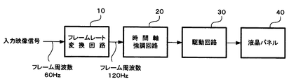
以下、本発明の画像表示装置について、添付図面を参照して説明する。図1は本発明の画像表示装置の第1実施形態を示すブロック図、図2は図1中のフレームレート変換回路10の具体的構成例を示すブロック図、図3は図1中のフレームレート変換回路10の動作を説明するための図、図4は図1中の時間軸強調回路20の具体的構成例を示すブロック図、図5及び図6は第1実施形態による効果を説明するための図、図7は本発明の画像表示装置の第2実施形態を示す部分ブロック図、図8は第2実施形態の動作を説明するためのタイミング図、図9は本発明の画像表示装置の第3実施形態を示す部分ブロック図、図10は本発明の画像表示装置の第4実施形態を示すブロック図、図11は第4実施形態の具体的構成例を示す部分ブロック図、図12は図10中のフレームレート変換回路11の動作を説明するための図、図13は第4実施形態の動作を説明するためのタイミング図、図14はホールド型表示で発生する動画ぼやけを説明するための図である。
Hereinafter, an image display device of the present invention will be described with reference to the accompanying drawings. FIG. 1 is a block diagram showing a first embodiment of the image display apparatus of the present invention, FIG. 2 is a block diagram showing a specific configuration example of the frame
<第1実施形態>
第1実施形態は上述した第1の問題点を解決するものである。図1において、映像信号はフレームレート変換回路10に入力される。フレームレート変換回路10は入力された映像信号のフレーム周波数(垂直周波数)を2倍に変換して出力する。第1実施形態及び後述する第2,第3実施形態では、入力映像信号(原信号)のフレーム周波数をm/n倍に変換する。ここで、mは2以上の整数、nは1以上の整数であり、m>nという条件を満たす。第1〜第4実施形態では、m=2、n=1とし、入力映像信号のフレーム周波数60Hzを120Hzに変換する。
なお、フレーム周波数30Hzで2:1インターレースの映像信号については、予め順次走査変換によって、フレーム周波数60Hzの順次走査の映像信号に変換されているものとする。フレームレート変換回路10の具体的構成及び動作は後述する。
<First Embodiment>
The first embodiment solves the first problem described above. In FIG. 1, the video signal is input to the frame
It is assumed that a 2: 1 interlaced video signal at a frame frequency of 30 Hz is previously converted into a progressively scanned video signal at a frame frequency of 60 Hz by sequential scanning conversion. The specific configuration and operation of the frame
フレームレート変換回路10より出力されたフレーム周波数120Hzの映像信号は時間軸強調回路20に入力される。時間軸強調回路20は入力された映像信号の時間軸方向の高域成分を強調して出力する。フレームレート変換回路10及び時間軸強調回路20の具体的構成及び動作は後述する。時間軸強調回路20より出力された映像信号は駆動回路30に入力され、駆動回路30はホールド型表示装置(表示パネル)の一例としての液晶パネル40を駆動してフレーム周波数120Hzの映像信号を表示する。表示パネルは液晶パネルに限定されることはなく、マトリクス状に配列された複数の画素を有し、電気信号を各画素毎に所定時間保持して表示するアクティブマトリクス型表示パネルであればよい。
The video signal having a frame frequency of 120 Hz output from the frame
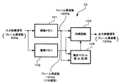
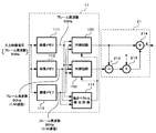
フレーム周波数変換回路10は一例として図2のように構成される。図2において、入力映像信号は画像メモリ101及び102に書き込まれる。画像メモリ101,102からはそれぞれ1フレーム分、合わせて2フレーム分の画像データが書き込み速度の2倍の速度で同時に読み出される。但し、画像メモリ102より出力される画像データは画像メモリ101より出力される画像データに対して1/60秒遅延されたものである。
画像メモリ101,102より出力された画像データは動きベクトル検出回路103と内挿回路104に供給される。動きベクトル検出回路103は一例としてマッチング法を用いてフレーム間の動きベクトルを検出する。内挿回路104は画像メモリ101,102から読み出された2フレーム分の画像データと動きベクトル検出回路103からの動きベクトルデータとから動き補償補間を行ってフレーム周波数120Hzの映像信号を出力する。
The frame
Image data output from the
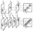
内挿回路104における動き補償補間は、フレーム周波数の変換比率が2倍であることから、図3に示すようにベクトル移動を行うものである。図3において、(A)は内挿回路104への入力映像信号を、(B)は内挿回路104からの出力映像信号を示している。入力映像信号のフレーム番号をF1,F2,F3…とし、出力映像信号のフレーム番号をf1a,f1b,f2a,f2b,f3a…とする。フレームF1からフレームf1aへの変換と、フレームF2からフレームf2aへの変換とフレームF3からフレームf3aへの変換は時間位相が一致しているので、ベクトル移動を行わない。フレームf1bはベクトル移動を行ってフレームF1,F2間に挿入され、フレームf2bはベクトル移動を行ってフレームF2,F3間に挿入される。
The motion compensation interpolation in the
図3(A),(B)の右側には、フレームF1〜F3,フレームf1a〜f3aに渡る物体Oの移動の様子を示している。図3(A)において、物体OはフレームF1における位置からフレームF2における位置へと動きベクトルV1にて移動し、フレームF2における位置からフレームF3における位置へと動きベクトルV2にて移動する。図3(B)において、フレームf1a,f2a,f3aにおける物体Oの位置はそれぞれフレームF1,F2,F3と同じである。フレームf1bの画像を生成するには、フレームF1の画像をV1/2だけ移動させればよく、フレームf2bの画像を生成するには、フレームF2の画像をV2/2だけ移動させればよい。 The right side of FIGS. 3A and 3B shows the movement of the object O across the frames F1 to F3 and the frames f1a to f3a. In FIG. 3 (A), the object O is moved at vector V 1 move to the position in the frame F2 from the position in the frame F1, moves upon vector V 2 moves to a position in the frame F3 from the position in the frame F2. In FIG. 3B, the position of the object O in the frames f1a, f2a, and f3a is the same as the frames F1, F2, and F3, respectively. To generate an image of the frame f1b may be moved to the image of the frame F1 by V 1/2, to generate an image of the frame f2b is, if moving an image of the frame F2 by V 2/2 Good.
図3に示す例では、フレームf1bを生成する際にはフレームF1の画像データのみを用い、フレームf2bを生成する際にはフレームF2の画像データのみを用いているが、前後のフレームを混合してもよい。フレームF1,F3の画像データを合成してもよい。この場合、フレームf1bは、フレームF1の画像をV1/2だけ移動したF1’とフレームF2の画像を−V1/2だけ移動したF2’を求め、F1’とF2’を1:1の割合で混合することによって得られる。また、フレームf2bは、フレームF2の画像をV2/2だけ移動したF2”とフレームF3の画像を−V2/2だけ移動したF3’を求め、F2”とF3’を1:1の割合で混合することによって得られる。ここに示す混合比は一例であり、この例に限定されるものではない。
このように、出力映像信号のフレームを生成する際に、1つのフレームだけでなく複数のフレームを用いて内挿を行うと、ノイズを低減することができるという効果を奏する。
In the example shown in FIG. 3, only the image data of the frame F1 is used when generating the frame f1b, and only the image data of the frame F2 is used when generating the frame f2b. May be. The image data of the frames F1 and F3 may be combined. In this case, for the frame f1b, F1 ′ obtained by moving the image of the frame F1 by V 1/2 and F2 ′ obtained by moving the image of the frame F2 by −V 1/2 are obtained, and F1 ′ and F2 ′ are set to 1: 1. Obtained by mixing in proportions. The frame f2b is "'seek, F2 and F3 has moved the image of the frame F3 by -V 2/2 F3"' the image of the frame F2 has been moved by V 2/2 F2 1: 1 ratio of Obtained by mixing with. The mixing ratio shown here is an example, and the present invention is not limited to this example.
As described above, when generating the frame of the output video signal, if interpolation is performed using not only one frame but also a plurality of frames, it is possible to reduce noise.
時間軸強調回路20は一例として図4のように構成される。図4において、フレームレート変換回路10より出力されたフレーム周波数120Hzの映像信号をfinとすると、映像信号finは画像メモリ201に入力されて、1フレーム遅延した映像信号foutとして出力される。減算器202は映像信号finから映像信号foutを減算して、映像信号finと映像信号foutとの差分を乗算器203に供給する。乗算器203は入力された差分に係数aを乗算して加算器204に供給する。加算器204は映像信号finと乗算器203の出力とを加算して出力信号gとして出力する。出力信号gは次の(1)式にて表される。
g=fin+a(fin−fout) …(1)
係数aは液晶の応答特性に応じて設定される。応答が比較的速く残像が少ない場合にはaを小さく設定し、応答が遅く残像が多い場合にはaを大きく設定する。
The time
g = fin + a (fin−fout) (1)
The coefficient a is set according to the response characteristics of the liquid crystal. If the response is relatively fast and there are few afterimages, a is set small, and if the response is slow and there are many afterimages, a is set large.
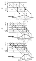
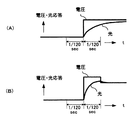
図5及び図6は第1実施形態による効果を示している。図5は黒,白,黒と並んだ矩形波形が水平方向に平行移動した場合の表示状態を示しており、(A)はフレーム周波数変換回路10によるフレームレート変換前のフレーム周波数60Hzの映像信号による表示状態、(B)はフレーム周波数変換回路10によるフレームレート変換後で、時間軸強調回路20による時間軸強調前のフレーム周波数120Hzの映像信号による表示状態、(C)はフレーム周波数変換回路10によるフレームレート変換及び時間軸強調回路20による時間軸強調後のフレーム周波数120Hzの映像信号による表示状態である。図5(A)〜(C)に示すように、水平方向に平行移動する黒,白,黒の矩形波形を、時間t方向に並べて表示している。
5 and 6 show the effects of the first embodiment. FIG. 5 shows a display state when rectangular waveforms arranged in black, white, and black are translated in the horizontal direction. FIG. 5A is a video signal having a frame frequency of 60 Hz before frame rate conversion by the frame
あるフレームから次のフレームに移って、黒,白,黒の矩形波形が水平方向に平行移動する際、白から黒、黒から白へと切り替わる部分において、人間の目には像が積分されて写る視覚系の積分という現象が起こるため、図5(A)〜(C)にそれぞれ示すように、黒から白へ及び白から黒へとなだらかに切り替わるように見え、動画ぼやけが発生することとなる。図5(A)〜(C)に示すように、視覚系の積分による動画ぼやけは、ホールド表示を行うことに起因するぼやけaと、液晶の応答速度に起因するぼやけbとよりなる。フレーム周波数60Hzの図5(A)では、ぼやけaとぼやけbのいずれも大きい。フレーム周波数120Hzの図5(B)では、ぼやけaの幅が狭くなり、動画ぼやけが改善されている。但し、ぼやけbは改善されていない。フレーム周波数120Hzで時間軸強調した図5(C)では、ぼやけbの幅も狭くなり、動画ぼやけがさらに改善されている。
図6(A),(B)はそれぞれ図5(B),(C)における一点鎖線にて示す断面pにおける電圧・光応答を示している。時間軸強調回路20による時間軸強調によって電圧・光応答は図6の(A)から(B)へと補正され、フレーム単位での表示特性が改善される。
When moving from one frame to the next and the black, white, and black rectangular waveforms move in the horizontal direction, the image is integrated into the human eye at the point where white to black and black to white are switched. Since the phenomenon of visual system integration occurs, as shown in FIGS. 5A to 5C, it seems that the video is gradually switched from black to white and from white to black, resulting in motion blur. Become. As shown in FIGS. 5A to 5C, the moving image blur due to the integration of the visual system is composed of a blur a resulting from the hold display and a blur b resulting from the response speed of the liquid crystal. In FIG. 5A with a frame frequency of 60 Hz, both blur a and blur b are large. In FIG. 5B with a frame frequency of 120 Hz, the width of the blur a is narrowed, and the moving image blur is improved. However, the blur b is not improved. In FIG. 5C in which the time axis is emphasized at a frame frequency of 120 Hz, the width of the blur b is also narrowed, and the moving image blur is further improved.
FIGS. 6A and 6B show the voltage / light response at the cross-section p indicated by the alternate long and short dash line in FIGS. 5B and 5C, respectively. By the time axis emphasis by the time
<第2実施形態>
第2実施形態は図1におけるフレームレート変換回路10と時間軸強調回路20との具体的構成を改良したものであり、具体的には図4における画像メモリ201を削除し、画像メモリ201の削除に伴ってフレームレート変換回路10の具体的構成を変更している。第2実施形態におけるフレームレート変換回路と時間軸強調回路をそれぞれフレームレート変換回路10’,時間軸強調回路20’と称することとする。図7において、図2及び図4と同一部分には同一符号を付し、その説明を適宜省略することがある。
Second Embodiment
In the second embodiment, the specific configuration of the frame
図7において、画像メモリ101,102より出力された画像データは動きベクトル検出回路103と内挿回路1041,1042に供給される。内挿回路1041は、図2の内挿回路104と実質的に同じであり、画像メモリ101,102から読み出された2フレーム分の画像データと動きベクトル検出回路103からの動きベクトルデータとから動き補償補間を行って、現在フレームの画像データを出力する。内挿回路1042は、画像メモリ101,102から読み出された2フレーム分の画像データと動きベクトル検出回路103からの動きベクトルデータとから動き補償補間を行って、1フレーム前の画像データを出力する。
内挿回路1041より出力された画像データは減算器202及び加算器204に供給され、内挿回路1042より出力された画像データは減算器202に供給される。
In FIG. 7, the image data output from the
The image data output from the
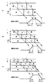
ここで、図8を用いてフレームレート変換回路10’の動作タイミングについて説明する。図8において、(A)はフレーム周波数60Hzの入力映像信号の画像データであり、(B),(C)に示すように、画像メモリ101,102から2回同じ画像データが読み出されてフレーム周波数120Hzの映像信号とされる。画像メモリ102より出力される画像データは画像メモリ101より出力される画像データに対して1/60秒遅延している。便宜上、図8(B)〜(F)のタイミングを図8(A)タイミングに対して一点鎖線で示すようにずらして図示している。
動きベクトル検出回路103は、図8(D)に示すように、画像メモリ101,102より出力された画像データを用いて動きベクトルV1,V1,V2,V2…を検出する。内挿回路1041は、図8(E)に示すように、フレームタイミングt1aにてフレームf1bを出力し、フレームタイミングt1bにてフレームf2aを出力する。内挿回路1042は、図8(F)に示すように、フレームタイミングt1aにてフレームf1aを出力し、フレームタイミングt1bにてフレームf1bを出力する。
Here, the operation timing of the frame
The motion
図8の(E)と(F)とを比較すれば分かるように、図8(F)の画像データは図8(E)の画像データより120Hz周期で1フレーム分遅延しているので、第2実施形態の時間軸強調回路20’においては、図4の時間軸強調回路20のように画像メモリ201を設ける必要はない。従って、第2実施形態は、第1実施形態よりも画像メモリを少なくすることができ、コスト削減が可能である。
As can be seen by comparing (E) and (F) in FIG. 8, the image data in FIG. 8 (F) is delayed by one frame at a period of 120 Hz from the image data in FIG. 8 (E). In the time
<第3実施形態>
第3実施形態は第2実施形態のフレームレート変換回路10’をさらに簡略化したものであり、第3実施形態におけるフレームレート変換回路をフレームレート変換回路10”と称することとする。図9において、図2,図4,図7と同一部分には同一符号を付し、その説明を適宜省略することがある。
画像メモリ101,102より出力された画像データは動きベクトル検出回路103と内挿回路104とセレクタ1051,1052に供給される。内挿回路104によって動き補償補間されて出力された画像データはセレクタ1051,1052に供給される。
セレクタ1051より出力された画像データは減算器202及び加算器204に供給され、セレクタ1052より出力された画像データは減算器202に供給される。
<Third Embodiment>
In the third embodiment, the frame
The image data output from the
The image data output from the
セレクタ1051,1052は、図8のフレームタイミングt1aで“0”側を選択し、フレームタイミングt1bで“1”側を選択する。図3にて説明したように、ベクトル移動を伴う内挿画像の生成は、フレームf1b,f2b…に限られ、動きベクトル検出回路103の結果によって内挿処理した画像データを出力するのは、1つのフレームタイミングでセレクタ1051,1052のいずれか一方だけであるため、図9のように簡略化した構成とすることができる。
第3実施形態では、第2実施形態と比較してセレクタ1051,1052が必要となるが、回路規模が比較的大きい内挿回路が内挿回路104の1つのみとなるので、さらにコスト削減が可能である。
The
In the third embodiment,
<第4実施形態>
第4実施形態は上述した第1及び第2の問題点を解決するものである。図14を用いてホールド型表示装置における動画ぼやけの発生とその低減の原理について改めて説明する。図14は図5,図6で説明したような時間軸強調を行っていおらず、液晶の応答速度に起因するぼやけbを無視してホールド表示を行うことに起因するぼやけaのみが発生した状態を図示している。
図14は黒,白,黒と並んだ矩形波形が水平方向に平行移動した場合の表示状態を示している。なお、映像信号(原信号)のフレーム周波数をNTSC方式等の60Hzとする。図14において、(A)はフレーム周波数を原信号のままの60Hzとした場合、(B)は後述する第4実施形態の好適な一例であるフレーム周波数を原信号の3/2倍の90Hzとした場合、(C)は上述した非特許文献1に記載されており、上述した第1〜第3実施形態のようにフレーム周波数を原信号の2倍の120Hzとした場合である。図14(A)〜(C)に示すように、水平方向に平行移動する黒,白,黒の矩形波形を、時間t方向に並べて表示している。
<Fourth embodiment>
The fourth embodiment solves the first and second problems described above. With reference to FIG. 14, the generation of moving image blur in the hold type display device and the principle of reduction thereof will be described again. 14 does not perform time axis enhancement as described with reference to FIGS. 5 and 6, and only the blur a resulting from hold display ignoring the blur b resulting from the response speed of the liquid crystal has occurred. Is illustrated.
FIG. 14 shows a display state when rectangular waveforms arranged in black, white and black are translated in the horizontal direction. Note that the frame frequency of the video signal (original signal) is 60 Hz, such as the NTSC system. In FIG. 14, (A) shows the case where the frame frequency is set to 60 Hz as the original signal, and (B) shows a frame frequency which is a suitable example of the fourth embodiment described later as 90 Hz which is 3/2 times the original signal. In this case, (C) is described in
あるフレームから次のフレームに移って、黒,白,黒の矩形波形が水平方向に平行移動する際、白から黒、黒から白へと切り替わる部分において、人間の目には像が積分されて写る視覚系の積分という現象が起こるため、図14(A)〜(C)にそれぞれ示すように、黒から白へ及び白から黒へとなだらかに切り替わるように見える。従って、図14(A)〜(C)それぞれに示す幅の動画ぼやけが発生することとなる。図14(A)〜(C)より分かるように、フレーム周波数が高くなるに従って動画ぼやけの幅は小さくなる。図14(C)のフレーム周波数120Hzにおいては、非特許文献1に記載のように、50%デューティの間欠表示と同様の効果が得られる。図14(B)のフレーム周波数90Hzにおいては、約67%デューティの間欠表示と同程度の効果が得られる。
When moving from one frame to the next and the black, white, and black rectangular waveforms move in the horizontal direction, the image is integrated into the human eye at the point where white to black and black to white are switched. Since the phenomenon of integration of the visual system occurs, as shown in FIGS. 14A to 14C, it seems that the display is gradually switched from black to white and from white to black. Accordingly, the moving image blur having the width shown in each of FIGS. 14A to 14C occurs. As can be seen from FIGS. 14A to 14C, the moving image blur width decreases as the frame frequency increases. At the frame frequency of 120 Hz in FIG. 14C, as described in
以上の説明より分かるように、フレーム周波数を上げれば上げるほどインパルス型表示に近付き、動画ぼやけはより低減されることになる。しかしながら、フレーム周波数を2倍を越える整数倍に上げたとしても、液晶の応答速度の限界があり、フレーム周波数を上げる効果が薄れてしまう。よって、フレーム周波数を上げれば上げるほどいいというものではない。現在、最も主流のWXGAの画素数は1280ドット×768ラインであり、ブランキング期間を無視して有効映像期間だけのサンプリング周波数を計算すると、フレーム周波数120Hzの場合、サンプリング周波数は118MHzとなる。この118MHzというサンプリング周波数は回路の動作速度や、回路間(例えば、フレームレート変換回路と駆動回路との間)の接続インターフェースにとって極めて大きな負担となる。従って、フレーム周波数を120Hzとすることは実現上の困難さを伴い、現実の製品として採用することは難しい。 As can be seen from the above description, the higher the frame frequency, the closer to the impulse-type display, and the moving image blur is further reduced. However, even if the frame frequency is increased to an integral multiple exceeding twice, the response speed of the liquid crystal is limited, and the effect of increasing the frame frequency is diminished. Therefore, the higher the frame frequency, the better. At present, the most mainstream WXGA pixel count is 1280 dots × 768 lines, and if the sampling frequency for the effective video period is calculated ignoring the blanking period, the sampling frequency is 118 MHz when the frame frequency is 120 Hz. The sampling frequency of 118 MHz is a very heavy burden on the operation speed of the circuit and the connection interface between the circuits (for example, between the frame rate conversion circuit and the drive circuit). Therefore, setting the frame frequency to 120 Hz is accompanied by difficulty in realization, and is difficult to adopt as an actual product.
そこで第4実施形態は、動画ぼやけを効果的に低減することができ、かつ、現実の製品として採用するができるフレーム周波数(垂直周波数)について鋭意検討したものである。第4実施形態では、入力映像信号(原信号)のフレーム周波数をm/n倍に変換する。ここで、mは3以上の整数、nは2以上の整数であり、m>nでかつm/nは整数にならないという条件を満たす。m,nの好適な例としては、m=3、n=2である。以下詳述する第4実施形態では、m=3、n=2とし、入力映像信号のフレーム周波数60Hzを90Hzに変換する。本発明者は、フレーム周波数を上述した非特許文献1に記載されている120Hzにしなくても、90Hzで動画ぼやけを十分効果的に低減できることを実験によって確認した。表示パネルの表示動作能力を考慮すると、変換後のフレーム周波数は100Hz以下とするのがよい。
Therefore, in the fourth embodiment, the frame frequency (vertical frequency) that can effectively reduce motion blur and can be adopted as an actual product has been intensively studied. In the fourth embodiment, the frame frequency of the input video signal (original signal) is converted to m / n times. Here, m is an integer of 3 or more, n is an integer of 2 or more, and the condition that m> n and m / n is not an integer is satisfied. Preferable examples of m and n are m = 3 and n = 2. In the fourth embodiment described in detail below, m = 3 and n = 2, and the frame frequency 60 Hz of the input video signal is converted to 90 Hz. The inventor has confirmed through experiments that the moving image blur can be sufficiently effectively reduced at 90 Hz without setting the frame frequency to 120 Hz described in
フレーム周波数が90Hzの場合、上記のように約67%デューティの間欠表示と同程度の効果があり、シャッタ期間が約33%である場合に相当する。このシャッタ期間は時間に換算すると約5.56msである。これは、液晶の応答速度の改善度としては相当大きなものである。さらに、フレーム周波数が90Hzの場合、映像信号のサンプリング周波数は原信号のサンプリング周波数の1.5倍であり、約88.5MHzでよい。この約88.5MHzというサンプリング周波数は、現状の集積回路(IC)の動作速度にとって、また、回路間の接続インターフェースにとって十分に実現可能な値である。 When the frame frequency is 90 Hz, the same effect as the intermittent display with a duty of about 67% is obtained as described above, which corresponds to the case where the shutter period is about 33%. This shutter period is about 5.56 ms in terms of time. This is a significant improvement in the response speed of the liquid crystal. Further, when the frame frequency is 90 Hz, the sampling frequency of the video signal is 1.5 times the sampling frequency of the original signal, and may be about 88.5 MHz. This sampling frequency of about 88.5 MHz is a value sufficiently realizable for the operation speed of the current integrated circuit (IC) and for the connection interface between the circuits.
ところで、1280ドット×720ライン(いわゆる720Pフォーマット)の液晶パネルが使われることも多い。この場合、フレーム周波数90Hzでのサンプリング周波数は約82.9MHzであり、実現が容易であり、現実の製品として採用可能であることが分かる。なお、フレーム周波数120Hzとすると、サンプリング周波数は110.6MHzとなってしまう。フレーム周波数変換後の映像信号のサンプリング周波数(フレーム周波数×垂直ライン数×水平画素数)が100MHz以下であることが好ましい。サンプリング周波数が100MHz以下であれば、集積回路の動作速度や回路間の接続インターフェースの点からも支障となることはない。 By the way, a liquid crystal panel of 1280 dots × 720 lines (so-called 720P format) is often used. In this case, the sampling frequency at the frame frequency of 90 Hz is about 82.9 MHz, which is easy to realize and can be adopted as an actual product. If the frame frequency is 120 Hz, the sampling frequency is 110.6 MHz. It is preferable that the sampling frequency of the video signal after frame frequency conversion (frame frequency × number of vertical lines × number of horizontal pixels) is 100 MHz or less. If the sampling frequency is 100 MHz or less, there is no problem in terms of the operation speed of the integrated circuit and the connection interface between the circuits.
第4実施形態の全体構成例は図10に示す通りである。図10において、フレームレート変換回路11にはフレーム周波数60Hzの順次走査信号である映像信号が入力される。フレームレート変換回路11は入力映像信号のフレーム周波数を3/2倍、即ち、90Hzに変換して出力する。フレーム周波数90Hzの映像信号は時間軸強調回路21に入力される。時間軸強調回路21は入力された映像信号を時間軸強調して出力する。フレームレート変換回路11及び時間軸強調回路21の具体的構成及び動作は後述する。時間軸強調回路21より出力された映像信号は駆動回路31に入力され、駆動回路31はホールド型表示装置(表示パネル)の一例としての液晶パネル41を駆動してフレーム周波数90Hzの映像信号を表示する。
An example of the overall configuration of the fourth embodiment is as shown in FIG. In FIG. 10, the frame
フレームレート変換回路11及び時間軸強調回路21は一例として図11に示すように構成される。図11において、フレーム周波数60Hzの映像信号は画像メモリ111〜113に入力される。画像メモリ111〜113にはそれぞれ1フレーム分の画像データが書き込み周波数60Hzにて書き込まれ、入力映像信号の3/2倍の速度である読み出し周波数90Hzにて同時に読み出される。但し、画像メモリ112より出力される画像データは画像メモリ111より出力される画像データに対して1/60秒遅延されたものであり、画像メモリ113より出力される画像データは画像メモリ111より出力される画像データに対して2/60秒遅延されたものである。
As an example, the frame
画像メモリ111〜113より読み出された画像データは動きベクトル検出回路114及び内挿回路1151,1152に入力される。動きベクトル検出回路114は画像メモリ111〜113からの3フレーム分の画像データを基にし、マッチング法等を用いてフレーム間の動きベクトルを検出する。内挿回路1151,1152は、画像メモリ111〜113からの3フレーム分の画像データと動きベクトル検出回路12にて検出された動きベクトルとを用いて動き補償補間を行う。
内挿回路1151より出力された画像データは減算器212及び加算器214に供給され、内挿回路1152より出力された画像データは減算器212に供給される。第4実施形態の時間軸強調回路21は、第2実施形態の時間軸強調回路20’と実質的に同じである。
The image data read from the
The image data output from the
内挿回路1151,1152における動き補償補間は、フレーム周波数の変換比率が3/2倍であることから、図12に示すようにベクトル移動を行うものである。図12において、(A)は内挿回路1151,1152への入力映像信号を、(B)は内挿回路1151,1152からの出力映像信号を示している。入力映像信号のフレーム番号をF1,F2,F3…とし、出力映像信号のフレーム番号をf1,f2a,f2b,f3…とする。フレームF1からフレームf1への変換及びフレームF3からフレームf3への変換は時間位相が一致しているので、ベクトル移動を行わない。フレームf2aはベクトル移動を行ってフレームF1,F2間に挿入され、フレームf2bはベクトル移動を行ってフレームF2,F3間に挿入される。
The motion compensated interpolation in the
図12(A),(B)の右側には、フレームF1〜F3,フレームf1〜f3に渡る物体Oの移動の様子を示している。図12(A)において、物体OはフレームF1における位置からフレームF2における位置へと動きベクトルV1にて移動し、フレームF2における位置からフレームF3における位置へと動きベクトルV2にて移動する。図12(B)において、フレームf1,f3における物体Oの位置はそれぞれフレームF1,F3と同じである。フレームF2での物体Oの位置を破線にて示している。フレームf2aの画像を生成するには、フレームF2の画像を−V1/3だけ移動させればよく、フレームf2bの画像を生成するには、フレームF2の画像をV2/3だけ移動させればよい。 On the right side of FIGS. 12A and 12B, the movement of the object O across the frames F1 to F3 and the frames f1 to f3 is shown. In FIG. 12 (A), the object O is moved at vector V 1 move to the position in the frame F2 from the position in the frame F1, moves upon vector V 2 moves to a position in the frame F3 from the position in the frame F2. In FIG. 12B, the position of the object O in the frames f1 and f3 is the same as that in the frames F1 and F3, respectively. The position of the object O in the frame F2 is indicated by a broken line. To generate an image of the frame f2a may be moved to the image of the frame F2 by -V 1/3, to generate an image of the frame f2b is caused to move the image of the frame F2 by V 2/3 That's fine.
図12に示す例では、フレームf2a,f2bを生成する際、フレームF2の画像データのみを用いているが、フレームF1,F3の画像データを合成してもよい。この場合、フレームf2aは、フレームF1の画像をV1×2/3だけ移動したF1’とフレームF2の画像を−V1×1/3だけ移動したF2’を求め、F1’とF2’を1:2の割合で混合することによって得られる。また、フレームf2bは、フレームF2の画像をV2×1/3だけ移動したF2”とフレームF3の画像を−V2×2/3だけ移動したF3’を求め、F2”とF3’を2:1の割合で混合することによって得られる。
ここに示す混合比は一例であり、この例に限定されるものではない。このように、出力映像信号のフレームを生成する際に、最も近接したフレームだけでなくこれに隣接するフレームも加えて内挿を行うと、ノイズを低減することができるという効果を奏する。
In the example shown in FIG. 12, when generating the frames f2a and f2b, only the image data of the frame F2 is used, but the image data of the frames F1 and F3 may be synthesized. In this case, for the frame f2a, F1 ′ obtained by moving the image of the frame F1 by V 1 × 2/3 and F2 ′ obtained by moving the image of the frame F2 by −V 1 × 1/3 are obtained, and F1 ′ and F2 ′ are obtained. It is obtained by mixing at a ratio of 1: 2. Also, for the frame f2b, F2 ″ obtained by moving the image of the frame F2 by V 2 × 1/3 and F3 ′ obtained by moving the image of the frame F3 by −V 2 × 2/3 are obtained, and F2 ″ and F3 ′ are set to 2 Obtained by mixing at a ratio of: 1.
The mixing ratio shown here is an example, and the present invention is not limited to this example. As described above, when the frame of the output video signal is generated, if interpolation is performed by adding not only the closest frame but also a frame adjacent thereto, an effect is obtained that noise can be reduced.
ここで、図13を用いてフレームレート変換回路11の動作タイミングについて説明する。図13において、(A)はフレーム周波数60Hzの入力映像信号の画像データであり、画像メモリ113〜111からは(B)〜(D)に示すように画像データが読み出されてフレーム周波数90Hzの映像信号とされる。便宜上、図13(B)〜(F)のタイミングを図13(A)タイミングに対して一点鎖線で示すようにずらして図示している。
図13(E),(F)より分かるように、内挿回路1152より出力される画像データは内挿回路1151より出力される画像データに対してフレーム周波数90Hzのレートで1フレーム分遅延した関係となっている。これにより、第4実施形態では、第2実施形態と同様、時間軸強調回路21内に画像メモリを設ける必要がない。
Here, the operation timing of the frame
As can be seen from FIGS. 13E and 13F, the image data output from the
第4実施形態の他の例として、m/nを4/3倍としてフレーム周波数を80Hzに変換したり、m/nを5/4倍としてフレーム周波数を75Hzに変換したり、m/nを6/5倍としてフレーム周波数を72Hzに変換する等が考えられる。第4実施形態によれば、非特許文献1に記載のバックライトをシャッタする手段を用いる場合と比較して表示パネルに対して動作不安定要因を与えることがなく、有利である。また、前述のように第4実施形態においては回路動作に対して大きな負担とならず、実用上に極めて有効である。
第4実施形態のさらに他の例として、フレームレート変換回路11及び時間軸強調回路21を、図9の第3実施形態のようにセレクタを用いることによって内挿回路を1つとした構成とすることもできる。
As another example of the fourth embodiment, m / n is 4/3 times to convert the frame frequency to 80 Hz, m / n is 5/4 times to convert the frame frequency to 75 Hz, or m / n is For example, the frame frequency may be converted to 72 Hz by 6/5 times. According to the fourth embodiment, compared with the case where the means for shuttering the backlight described in
As still another example of the fourth embodiment, the frame
10,11 フレームレート変換回路
20,21 時間軸強調回路
30,31 駆動回路
40,41液晶パネル(表示パネル)
101,102,111〜113 画像メモリ
103,114 動きベクトル検出回路
104,1041,1042,1151,1152 内挿回路
1051,1052 セレクタ
10, 11 Frame
101, 102, 111-113
1051, 1052 selector
Claims (2)
第1の垂直周波数を有する映像信号を、前記第1の垂直周波数のm/n倍(ここで、mは2以上の整数、nは1以上の整数であり、m>nという条件を満たす)である第2の垂直周波数に変換して出力するレート変換回路と、
前記レート変換回路より出力された前記第2の垂直周波数を有する映像信号における隣接する2フレーム分の画像データを用いて時間軸方向の高域成分を強調する時間軸強調回路と、
前記時間軸強調回路より出力された前記第2の垂直周波数を有する映像信号を前記アクティブマトリクス型表示パネルに表示する駆動回路とを備え、
前記レート変換回路は、
前記第1の垂直周波数を有する映像信号を書き込んで前記第2の垂直周波数の映像信号として出力する複数の画像メモリと、
前記複数の画像メモリより出力された画像データを用いて動きベクトルを検出する動きベクトル検出回路と、
前記複数の画像メモリより出力された画像データと前記動きベクトルとを用いて動き補償補間して、前記第2の垂直周波数の映像信号であり互いに1フレーム分ずれた関係にある画像データを出力する第1及び第2の内挿回路とを有し、
前記時間軸強調回路は、
前記隣接する2フレーム分の画像データとして前記第1及び第2の内挿回路より出力された画像データを用いて時間軸方向の高域成分を強調する
ことを特徴とする画像表示装置。 A plurality of pixels arranged in a matrix in an image display device using an active matrix type display panel for displaying holding a predetermined time an electrical signal to the image Motogoto,
A video signal having a first vertical frequency is m / n times the first vertical frequency (where m is an integer of 2 or more, n is an integer of 1 or more, and a condition of m> n is satisfied). A rate conversion circuit for converting to a second vertical frequency and outputting,
A time axis emphasizing circuit for emphasizing a high frequency component in the time axis direction using image data for two adjacent frames in the video signal having the second vertical frequency output from the rate conversion circuit;
A drive circuit for displaying the video signal having the second vertical frequency output from the time axis emphasizing circuit on the active matrix display panel ;
The rate conversion circuit
A plurality of image memories for writing a video signal having the first vertical frequency and outputting the video signal as the second vertical frequency;
A motion vector detection circuit for detecting a motion vector using image data output from the plurality of image memories;
The image data output from the plurality of image memories and the motion vector are used for motion compensation interpolation, and the second vertical frequency video signal that is shifted by one frame from each other is output. First and second interpolation circuits,
The time axis emphasis circuit is
An image display device characterized by emphasizing a high frequency component in a time axis direction using image data output from the first and second interpolation circuits as image data for two adjacent frames .
第1の垂直周波数を有する映像信号を、前記第1の垂直周波数のm/n倍(ここで、mは2以上の整数、nは1以上の整数であり、m>nという条件を満たす)である第2の垂直周波数に変換して出力するレート変換回路と、
前記レート変換回路より出力された前記第2の垂直周波数を有する映像信号における隣接する2フレーム分の画像データを用いて時間軸方向の高域成分を強調する時間軸強調回路と、
前記時間軸強調回路より出力された前記第2の垂直周波数を有する映像信号を前記アクティブマトリクス型表示パネルに表示する駆動回路とを備え、
前記レート変換回路は、
前記第1の垂直周波数を有する映像信号を書き込んで前記第2の垂直周波数の映像信号として出力する複数の画像メモリと、
前記複数の画像メモリより出力された画像データを用いて動きベクトルを検出する動きベクトル検出回路と、
前記複数の画像メモリより出力された画像データと前記動きベクトルとを用いて動き補償補間して、前記第2の垂直周波数の映像信号を出力する内挿回路と、
前記複数の画像メモリより出力された画像データと前記内挿回路より出力された画像データとを選択的に出力することにより互いに1フレーム分ずれた関係にある画像データを出力する第1及び第2のセレクタとを有し、
前記時間軸強調回路は、
前記隣接する2フレーム分の画像データとして前記第1及び第2のセレクタより出力された画像データを用いて時間軸方向の高域成分を強調する
ことを特徴とする画像表示装置。 In an image display device using an active matrix display panel having a plurality of pixels arranged in a matrix and displaying an electric signal for each pixel for a predetermined time,
A video signal having a first vertical frequency is m / n times the first vertical frequency (where m is an integer of 2 or more, n is an integer of 1 or more, and a condition of m> n is satisfied). A rate conversion circuit for converting to a second vertical frequency and outputting,
A time axis emphasizing circuit for emphasizing a high frequency component in the time axis direction using image data for two adjacent frames in the video signal having the second vertical frequency output from the rate conversion circuit;
A drive circuit for displaying the video signal having the second vertical frequency output from the time axis emphasizing circuit on the active matrix display panel;
The rate conversion circuit
A plurality of image memories for writing a video signal having the first vertical frequency and outputting the video signal as the second vertical frequency;
A motion vector detection circuit for detecting a motion vector using image data output from the plurality of image memories;
An interpolation circuit for performing motion compensation interpolation using the image data output from the plurality of image memories and the motion vector, and outputting the video signal of the second vertical frequency;
First and second output image data having a relationship shifted by one frame by selectively outputting image data output from the plurality of image memories and image data output from the interpolation circuit And a selector
The time axis emphasis circuit is
An image display device characterized by emphasizing a high frequency component in a time axis direction using image data output from the first and second selectors as image data for two adjacent frames .
Priority Applications (3)
| Application Number | Priority Date | Filing Date | Title |
|---|---|---|---|
| JP2003387660A JP4367100B2 (en) | 2003-11-18 | 2003-11-18 | Image display device |
| US10/959,078 US7400321B2 (en) | 2003-10-10 | 2004-10-07 | Image display unit |
| US12/155,172 US8063861B2 (en) | 2003-10-10 | 2008-05-30 | Image display unit |
Applications Claiming Priority (1)
| Application Number | Priority Date | Filing Date | Title |
|---|---|---|---|
| JP2003387660A JP4367100B2 (en) | 2003-11-18 | 2003-11-18 | Image display device |
Related Child Applications (1)
| Application Number | Title | Priority Date | Filing Date |
|---|---|---|---|
| JP2009165374A Division JP4556198B2 (en) | 2009-07-14 | 2009-07-14 | Image display device |
Publications (2)
| Publication Number | Publication Date |
|---|---|
| JP2005148521A JP2005148521A (en) | 2005-06-09 |
| JP4367100B2 true JP4367100B2 (en) | 2009-11-18 |
Family
ID=34694952
Family Applications (1)
| Application Number | Title | Priority Date | Filing Date |
|---|---|---|---|
| JP2003387660A Expired - Lifetime JP4367100B2 (en) | 2003-10-10 | 2003-11-18 | Image display device |
Country Status (1)
| Country | Link |
|---|---|
| JP (1) | JP4367100B2 (en) |
Families Citing this family (20)
| Publication number | Priority date | Publication date | Assignee | Title |
|---|---|---|---|---|
| JP5062968B2 (en) | 2004-08-11 | 2012-10-31 | ソニー株式会社 | Image processing apparatus and method, recording medium, and program |
| EP1777939A4 (en) * | 2004-08-11 | 2011-04-13 | Sony Corp | Image processing apparatus and method, recording medium, and program |
| JP4548065B2 (en) * | 2004-09-24 | 2010-09-22 | 日本ビクター株式会社 | Image processing device |
| KR101182298B1 (en) * | 2005-09-12 | 2012-09-20 | 엘지디스플레이 주식회사 | Apparatus and method for driving liquid crystal display device |
| KR100747290B1 (en) * | 2005-11-07 | 2007-08-07 | 엘지전자 주식회사 | Device and metheod for reducing Motion Blur in Liquid Crystal Display |
| EP1949360B1 (en) * | 2005-11-10 | 2013-02-20 | Chimei InnoLux Corporation | Display device and driving method therefor |
| KR101201317B1 (en) | 2005-12-08 | 2012-11-14 | 엘지디스플레이 주식회사 | Apparatus and method for driving liquid crystal display device |
| KR20070117295A (en) * | 2006-06-08 | 2007-12-12 | 삼성전자주식회사 | Liquid crystal display device and driving integrated circuit chip thereof |
| KR101463035B1 (en) * | 2006-10-23 | 2014-11-20 | 삼성디스플레이 주식회사 | Liquid crystal display and method for driving the same |
| US8259226B2 (en) | 2006-11-24 | 2012-09-04 | Sharp Kabushiki Kaisha | Image display device |
| WO2008102826A1 (en) | 2007-02-20 | 2008-08-28 | Sony Corporation | Image display device, video signal processing device, and video signal processing method |
| JP5117762B2 (en) | 2007-05-18 | 2013-01-16 | 株式会社半導体エネルギー研究所 | Liquid crystal display |
| KR100953143B1 (en) | 2007-05-21 | 2010-04-16 | 닛뽕빅터 가부시키가이샤 | Image signal display apparatus and image signal display method |
| JP4964197B2 (en) * | 2008-07-18 | 2012-06-27 | 株式会社Jvcケンウッド | Video signal processing apparatus and video signal processing method |
| JP2010197548A (en) | 2009-02-24 | 2010-09-09 | Victor Co Of Japan Ltd | Image display device |
| US20110298774A1 (en) * | 2009-03-18 | 2011-12-08 | Sharp Kabushiki Kaisha | Display apparatus |
| KR101574080B1 (en) * | 2009-04-15 | 2015-12-04 | 삼성디스플레이 주식회사 | Method of processing data data processing device for performing the method and display apparatus having the data processing device |
| JP5702063B2 (en) * | 2009-12-14 | 2015-04-15 | ソニー株式会社 | Display device, display method, and computer program |
| JP5396524B2 (en) * | 2012-10-18 | 2014-01-22 | 株式会社半導体エネルギー研究所 | Liquid crystal display |
| JP5998982B2 (en) | 2013-02-25 | 2016-09-28 | 株式会社Jvcケンウッド | Video signal processing apparatus and method |
-
2003
- 2003-11-18 JP JP2003387660A patent/JP4367100B2/en not_active Expired - Lifetime
Also Published As
| Publication number | Publication date |
|---|---|
| JP2005148521A (en) | 2005-06-09 |
Similar Documents
| Publication | Publication Date | Title |
|---|---|---|
| US8063861B2 (en) | Image display unit | |
| JP4367100B2 (en) | Image display device | |
| JP4569388B2 (en) | Image display device | |
| JP4306671B2 (en) | Moving image display device and moving image display method | |
| KR100613116B1 (en) | Image display device | |
| JP4453647B2 (en) | Moving image display device and moving image display method | |
| JP5335293B2 (en) | Liquid crystal display device and driving method thereof | |
| JP5174363B2 (en) | Display system | |
| JP5049703B2 (en) | Image display device, image processing circuit and method thereof | |
| JP4884481B2 (en) | Image display device | |
| JP2008118505A (en) | Image display and displaying method, a image processor and processing method | |
| JP4548065B2 (en) | Image processing device | |
| JP2009109694A (en) | Display unit | |
| JP2005268912A (en) | Image processor for frame interpolation and display having the same | |
| JP2011059312A (en) | Image display device and control method of the same | |
| JP4556198B2 (en) | Image display device | |
| JP2003005723A (en) | Liquid crystal display device and electronic equipment | |
| JP2008009227A (en) | Image data output unit and liquid crystal display device | |
| JP4770290B2 (en) | Liquid crystal display | |
| JP2002132220A (en) | Method for displaying picture of liquid crystal display device and liquid crystal display device | |
| JP2005117529A (en) | Image display device | |
| JP2008040384A (en) | Video signal processing system and display apparatus using the same | |
| KR100747290B1 (en) | Device and metheod for reducing Motion Blur in Liquid Crystal Display | |
| JP2010101915A (en) | Image display device and image display method | |
| US8194185B2 (en) | Video picture display method to reduce the effects of blurring and double contours and device implementing this method |
Legal Events
| Date | Code | Title | Description |
|---|---|---|---|
| A621 | Written request for application examination |
Free format text: JAPANESE INTERMEDIATE CODE: A621 Effective date: 20060331 |
|
| A977 | Report on retrieval |
Free format text: JAPANESE INTERMEDIATE CODE: A971007 Effective date: 20090602 |
|
| A131 | Notification of reasons for refusal |
Free format text: JAPANESE INTERMEDIATE CODE: A131 Effective date: 20090612 |
|
| A521 | Request for written amendment filed |
Free format text: JAPANESE INTERMEDIATE CODE: A523 Effective date: 20090714 |
|
| TRDD | Decision of grant or rejection written | ||
| A01 | Written decision to grant a patent or to grant a registration (utility model) |
Free format text: JAPANESE INTERMEDIATE CODE: A01 Effective date: 20090804 |
|
| A01 | Written decision to grant a patent or to grant a registration (utility model) |
Free format text: JAPANESE INTERMEDIATE CODE: A01 |
|
| A61 | First payment of annual fees (during grant procedure) |
Free format text: JAPANESE INTERMEDIATE CODE: A61 Effective date: 20090817 |
|
| R151 | Written notification of patent or utility model registration |
Ref document number: 4367100 Country of ref document: JP Free format text: JAPANESE INTERMEDIATE CODE: R151 |
|
| FPAY | Renewal fee payment (event date is renewal date of database) |
Free format text: PAYMENT UNTIL: 20120904 Year of fee payment: 3 |
|
| FPAY | Renewal fee payment (event date is renewal date of database) |
Free format text: PAYMENT UNTIL: 20120904 Year of fee payment: 3 |
|
| S111 | Request for change of ownership or part of ownership |
Free format text: JAPANESE INTERMEDIATE CODE: R313111 |
|
| FPAY | Renewal fee payment (event date is renewal date of database) |
Free format text: PAYMENT UNTIL: 20120904 Year of fee payment: 3 |
|
| R350 | Written notification of registration of transfer |
Free format text: JAPANESE INTERMEDIATE CODE: R350 |
|
| FPAY | Renewal fee payment (event date is renewal date of database) |
Free format text: PAYMENT UNTIL: 20120904 Year of fee payment: 3 |
|
| FPAY | Renewal fee payment (event date is renewal date of database) |
Free format text: PAYMENT UNTIL: 20130904 Year of fee payment: 4 |
|
| EXPY | Cancellation because of completion of term |