JP4366187B2 - Card manufacturing method and resulting card - Google Patents
Card manufacturing method and resulting card Download PDFInfo
- Publication number
- JP4366187B2 JP4366187B2 JP2003520256A JP2003520256A JP4366187B2 JP 4366187 B2 JP4366187 B2 JP 4366187B2 JP 2003520256 A JP2003520256 A JP 2003520256A JP 2003520256 A JP2003520256 A JP 2003520256A JP 4366187 B2 JP4366187 B2 JP 4366187B2
- Authority
- JP
- Japan
- Prior art keywords
- circuit board
- layer
- face
- conductive
- conductive layer
- Prior art date
- Legal status (The legal status is an assumption and is not a legal conclusion. Google has not performed a legal analysis and makes no representation as to the accuracy of the status listed.)
- Expired - Fee Related
Links
Images


Classifications
-
- H—ELECTRICITY
- H05—ELECTRIC TECHNIQUES NOT OTHERWISE PROVIDED FOR
- H05K—PRINTED CIRCUITS; CASINGS OR CONSTRUCTIONAL DETAILS OF ELECTRIC APPARATUS; MANUFACTURE OF ASSEMBLAGES OF ELECTRICAL COMPONENTS
- H05K1/00—Printed circuits
- H05K1/02—Details
- H05K1/0213—Electrical arrangements not otherwise provided for
- H05K1/0254—High voltage adaptations; Electrical insulation details; Overvoltage or electrostatic discharge protection ; Arrangements for regulating voltages or for using plural voltages
- H05K1/0256—Electrical insulation details, e.g. around high voltage areas
-
- H—ELECTRICITY
- H05—ELECTRIC TECHNIQUES NOT OTHERWISE PROVIDED FOR
- H05K—PRINTED CIRCUITS; CASINGS OR CONSTRUCTIONAL DETAILS OF ELECTRIC APPARATUS; MANUFACTURE OF ASSEMBLAGES OF ELECTRICAL COMPONENTS
- H05K1/00—Printed circuits
- H05K1/02—Details
- H05K1/11—Printed elements for providing electric connections to or between printed circuits
-
- G—PHYSICS
- G06—COMPUTING; CALCULATING OR COUNTING
- G06K—GRAPHICAL DATA READING; PRESENTATION OF DATA; RECORD CARRIERS; HANDLING RECORD CARRIERS
- G06K19/00—Record carriers for use with machines and with at least a part designed to carry digital markings
- G06K19/06—Record carriers for use with machines and with at least a part designed to carry digital markings characterised by the kind of the digital marking, e.g. shape, nature, code
- G06K19/067—Record carriers with conductive marks, printed circuits or semiconductor circuit elements, e.g. credit or identity cards also with resonating or responding marks without active components
- G06K19/07—Record carriers with conductive marks, printed circuits or semiconductor circuit elements, e.g. credit or identity cards also with resonating or responding marks without active components with integrated circuit chips
- G06K19/077—Constructional details, e.g. mounting of circuits in the carrier
- G06K19/0772—Physical layout of the record carrier
- G06K19/07732—Physical layout of the record carrier the record carrier having a housing or construction similar to well-known portable memory devices, such as SD cards, USB or memory sticks
-
- G—PHYSICS
- G06—COMPUTING; CALCULATING OR COUNTING
- G06K—GRAPHICAL DATA READING; PRESENTATION OF DATA; RECORD CARRIERS; HANDLING RECORD CARRIERS
- G06K19/00—Record carriers for use with machines and with at least a part designed to carry digital markings
- G06K19/06—Record carriers for use with machines and with at least a part designed to carry digital markings characterised by the kind of the digital marking, e.g. shape, nature, code
- G06K19/067—Record carriers with conductive marks, printed circuits or semiconductor circuit elements, e.g. credit or identity cards also with resonating or responding marks without active components
- G06K19/07—Record carriers with conductive marks, printed circuits or semiconductor circuit elements, e.g. credit or identity cards also with resonating or responding marks without active components with integrated circuit chips
- G06K19/077—Constructional details, e.g. mounting of circuits in the carrier
- G06K19/0772—Physical layout of the record carrier
- G06K19/07735—Physical layout of the record carrier the record carrier comprising means for protecting against electrostatic discharge
-
- H—ELECTRICITY
- H05—ELECTRIC TECHNIQUES NOT OTHERWISE PROVIDED FOR
- H05K—PRINTED CIRCUITS; CASINGS OR CONSTRUCTIONAL DETAILS OF ELECTRIC APPARATUS; MANUFACTURE OF ASSEMBLAGES OF ELECTRICAL COMPONENTS
- H05K1/00—Printed circuits
- H05K1/02—Details
- H05K1/11—Printed elements for providing electric connections to or between printed circuits
- H05K1/117—Pads along the edge of rigid circuit boards, e.g. for pluggable connectors
-
- H—ELECTRICITY
- H05—ELECTRIC TECHNIQUES NOT OTHERWISE PROVIDED FOR
- H05K—PRINTED CIRCUITS; CASINGS OR CONSTRUCTIONAL DETAILS OF ELECTRIC APPARATUS; MANUFACTURE OF ASSEMBLAGES OF ELECTRICAL COMPONENTS
- H05K3/00—Apparatus or processes for manufacturing printed circuits
- H05K3/22—Secondary treatment of printed circuits
- H05K3/24—Reinforcing the conductive pattern
- H05K3/241—Reinforcing the conductive pattern characterised by the electroplating method; means therefor, e.g. baths or apparatus
- H05K3/242—Reinforcing the conductive pattern characterised by the electroplating method; means therefor, e.g. baths or apparatus characterised by using temporary conductors on the printed circuit for electrically connecting areas which are to be electroplated
-
- H—ELECTRICITY
- H01—ELECTRIC ELEMENTS
- H01L—SEMICONDUCTOR DEVICES NOT COVERED BY CLASS H10
- H01L2224/00—Indexing scheme for arrangements for connecting or disconnecting semiconductor or solid-state bodies and methods related thereto as covered by H01L24/00
- H01L2224/01—Means for bonding being attached to, or being formed on, the surface to be connected, e.g. chip-to-package, die-attach, "first-level" interconnects; Manufacturing methods related thereto
- H01L2224/42—Wire connectors; Manufacturing methods related thereto
- H01L2224/47—Structure, shape, material or disposition of the wire connectors after the connecting process
- H01L2224/48—Structure, shape, material or disposition of the wire connectors after the connecting process of an individual wire connector
- H01L2224/4805—Shape
- H01L2224/4809—Loop shape
- H01L2224/48091—Arched
-
- H—ELECTRICITY
- H01—ELECTRIC ELEMENTS
- H01L—SEMICONDUCTOR DEVICES NOT COVERED BY CLASS H10
- H01L2224/00—Indexing scheme for arrangements for connecting or disconnecting semiconductor or solid-state bodies and methods related thereto as covered by H01L24/00
- H01L2224/01—Means for bonding being attached to, or being formed on, the surface to be connected, e.g. chip-to-package, die-attach, "first-level" interconnects; Manufacturing methods related thereto
- H01L2224/42—Wire connectors; Manufacturing methods related thereto
- H01L2224/47—Structure, shape, material or disposition of the wire connectors after the connecting process
- H01L2224/48—Structure, shape, material or disposition of the wire connectors after the connecting process of an individual wire connector
- H01L2224/481—Disposition
- H01L2224/48151—Connecting between a semiconductor or solid-state body and an item not being a semiconductor or solid-state body, e.g. chip-to-substrate, chip-to-passive
- H01L2224/48221—Connecting between a semiconductor or solid-state body and an item not being a semiconductor or solid-state body, e.g. chip-to-substrate, chip-to-passive the body and the item being stacked
- H01L2224/48225—Connecting between a semiconductor or solid-state body and an item not being a semiconductor or solid-state body, e.g. chip-to-substrate, chip-to-passive the body and the item being stacked the item being non-metallic, e.g. insulating substrate with or without metallisation
- H01L2224/48227—Connecting between a semiconductor or solid-state body and an item not being a semiconductor or solid-state body, e.g. chip-to-substrate, chip-to-passive the body and the item being stacked the item being non-metallic, e.g. insulating substrate with or without metallisation connecting the wire to a bond pad of the item
-
- H—ELECTRICITY
- H05—ELECTRIC TECHNIQUES NOT OTHERWISE PROVIDED FOR
- H05K—PRINTED CIRCUITS; CASINGS OR CONSTRUCTIONAL DETAILS OF ELECTRIC APPARATUS; MANUFACTURE OF ASSEMBLAGES OF ELECTRICAL COMPONENTS
- H05K1/00—Printed circuits
- H05K1/02—Details
- H05K1/0213—Electrical arrangements not otherwise provided for
- H05K1/0254—High voltage adaptations; Electrical insulation details; Overvoltage or electrostatic discharge protection ; Arrangements for regulating voltages or for using plural voltages
- H05K1/0257—Overvoltage protection
- H05K1/0259—Electrostatic discharge [ESD] protection
-
- H—ELECTRICITY
- H05—ELECTRIC TECHNIQUES NOT OTHERWISE PROVIDED FOR
- H05K—PRINTED CIRCUITS; CASINGS OR CONSTRUCTIONAL DETAILS OF ELECTRIC APPARATUS; MANUFACTURE OF ASSEMBLAGES OF ELECTRICAL COMPONENTS
- H05K1/00—Printed circuits
- H05K1/02—Details
- H05K1/0266—Marks, test patterns or identification means
- H05K1/0268—Marks, test patterns or identification means for electrical inspection or testing
-
- H—ELECTRICITY
- H05—ELECTRIC TECHNIQUES NOT OTHERWISE PROVIDED FOR
- H05K—PRINTED CIRCUITS; CASINGS OR CONSTRUCTIONAL DETAILS OF ELECTRIC APPARATUS; MANUFACTURE OF ASSEMBLAGES OF ELECTRICAL COMPONENTS
- H05K1/00—Printed circuits
- H05K1/02—Details
- H05K1/0296—Conductive pattern lay-out details not covered by sub groups H05K1/02 - H05K1/0295
- H05K1/0298—Multilayer circuits
-
- H—ELECTRICITY
- H05—ELECTRIC TECHNIQUES NOT OTHERWISE PROVIDED FOR
- H05K—PRINTED CIRCUITS; CASINGS OR CONSTRUCTIONAL DETAILS OF ELECTRIC APPARATUS; MANUFACTURE OF ASSEMBLAGES OF ELECTRICAL COMPONENTS
- H05K2201/00—Indexing scheme relating to printed circuits covered by H05K1/00
- H05K2201/09—Shape and layout
- H05K2201/09145—Edge details
- H05K2201/0919—Exposing inner circuit layers or metal planes at the side edge of the PCB or at the walls of large holes
-
- H—ELECTRICITY
- H05—ELECTRIC TECHNIQUES NOT OTHERWISE PROVIDED FOR
- H05K—PRINTED CIRCUITS; CASINGS OR CONSTRUCTIONAL DETAILS OF ELECTRIC APPARATUS; MANUFACTURE OF ASSEMBLAGES OF ELECTRICAL COMPONENTS
- H05K2201/00—Indexing scheme relating to printed circuits covered by H05K1/00
- H05K2201/09—Shape and layout
- H05K2201/09209—Shape and layout details of conductors
- H05K2201/0929—Conductive planes
- H05K2201/093—Layout of power planes, ground planes or power supply conductors, e.g. having special clearance holes therein
-
- H—ELECTRICITY
- H05—ELECTRIC TECHNIQUES NOT OTHERWISE PROVIDED FOR
- H05K—PRINTED CIRCUITS; CASINGS OR CONSTRUCTIONAL DETAILS OF ELECTRIC APPARATUS; MANUFACTURE OF ASSEMBLAGES OF ELECTRICAL COMPONENTS
- H05K2201/00—Indexing scheme relating to printed circuits covered by H05K1/00
- H05K2201/09—Shape and layout
- H05K2201/09209—Shape and layout details of conductors
- H05K2201/0929—Conductive planes
- H05K2201/09309—Core having two or more power planes; Capacitive laminate of two power planes
-
- H—ELECTRICITY
- H05—ELECTRIC TECHNIQUES NOT OTHERWISE PROVIDED FOR
- H05K—PRINTED CIRCUITS; CASINGS OR CONSTRUCTIONAL DETAILS OF ELECTRIC APPARATUS; MANUFACTURE OF ASSEMBLAGES OF ELECTRICAL COMPONENTS
- H05K2201/00—Indexing scheme relating to printed circuits covered by H05K1/00
- H05K2201/09—Shape and layout
- H05K2201/09209—Shape and layout details of conductors
- H05K2201/09654—Shape and layout details of conductors covering at least two types of conductors provided for in H05K2201/09218 - H05K2201/095
- H05K2201/0969—Apertured conductors
-
- H—ELECTRICITY
- H05—ELECTRIC TECHNIQUES NOT OTHERWISE PROVIDED FOR
- H05K—PRINTED CIRCUITS; CASINGS OR CONSTRUCTIONAL DETAILS OF ELECTRIC APPARATUS; MANUFACTURE OF ASSEMBLAGES OF ELECTRICAL COMPONENTS
- H05K2203/00—Indexing scheme relating to apparatus or processes for manufacturing printed circuits covered by H05K3/00
- H05K2203/17—Post-manufacturing processes
- H05K2203/175—Configurations of connections suitable for easy deletion, e.g. modifiable circuits or temporary conductors for electroplating; Processes for deleting connections
-
- H—ELECTRICITY
- H05—ELECTRIC TECHNIQUES NOT OTHERWISE PROVIDED FOR
- H05K—PRINTED CIRCUITS; CASINGS OR CONSTRUCTIONAL DETAILS OF ELECTRIC APPARATUS; MANUFACTURE OF ASSEMBLAGES OF ELECTRICAL COMPONENTS
- H05K3/00—Apparatus or processes for manufacturing printed circuits
- H05K3/0011—Working of insulating substrates or insulating layers
- H05K3/0044—Mechanical working of the substrate, e.g. drilling or punching
- H05K3/0052—Depaneling, i.e. dividing a panel into circuit boards; Working of the edges of circuit boards
Abstract
Description
本発明は、一般に、回路基板と、回路基板を集積してメモリカードを作成する方法と、その結果得られるメモリカードとに関する。 The present invention generally relates to circuit boards, methods for integrating circuit boards to make memory cards, and the resulting memory cards.
本発明は、一般に、回路基板に関し、さらに詳細には、データを記憶するために携帯用デバイスにおいて利用されるメモリカードの回路基板に関する。本発明は多種多様の回路基板に利用されるものであるが、本明細書では、メモリカード、具体的にはフラッシュ型の電気的に消去可能でプログラム可能なリードオンリーメモリ(フラッシュEEPROM)を持つ携帯用メモリカードにおける本発明の実現について説明する。 The present invention relates generally to circuit boards, and more particularly to circuit boards for memory cards utilized in portable devices to store data. The present invention is used for a wide variety of circuit boards, but the present specification has a memory card, specifically a flash-type electrically erasable and programmable read-only memory (flash EEPROM). Implementation of the present invention in a portable memory card will be described.
近年、デジタルカメラ、デジタルオーディオプレーヤ、個人用情報機器などのデバイスがポピュラーになっている。これらのデバイスは、小さな堅固なパッケージの中に多量の記憶容量を必要とする。高密度の不揮発性メモリを利用するメモリカードの場合、これらのデバイスや、パーソナルコンピュータと接続されたプリンタおよび外部リーダーへの挿入や取り外しが頻繁に行われる。このような取り扱いを頻繁に受ける結果、これらカードには静電放電が発生するリスクが高くなる。 In recent years, devices such as digital cameras, digital audio players, and personal information devices have become popular. These devices require a large amount of storage capacity in a small, robust package. In the case of a memory card using a high-density non-volatile memory, insertion and removal of these devices, a printer connected to a personal computer, and an external reader are frequently performed. As a result of such frequent handling, these cards are at increased risk of electrostatic discharge.
したがって、静電放電から影響を受けず、しかも、製造組立が単純な小型の薄型メモリカードが望まれている。
メモリカードはますます小型でかつ薄型になり、しかもその容量が増大しているため、メモリカードの高密度化とパッケージ化がさらに進んでいる。このような取り扱いを頻繁に受ける結果、これらカードには静電放電(ESD)が発生するリスクが高くなる。 As memory cards are becoming smaller and thinner and their capacity is increasing, memory cards are becoming increasingly dense and packaged. As a result of such frequent handling, these cards have a higher risk of electrostatic discharge (ESD).
メモリカード、並びに、静電放電に起因する損傷に対してメモリカードを抵抗力のあるものにし、カードの複数の導電層が短絡の被害を受け難くするための方法について説明する。メモリカードは、プラスチックカバーの中へ回路基板を配置するカプセル化処理により形成される。プラスチックカバーと回路基板の端面との間の接合部に空隙部が在り、そこに静電放電が入って、メモリカードの回路素子への損傷が生じ易くなる。接地/電源層が、回路基板の端面まで、かつ、回路基板とメモリカードとの間の接合部に沿って延伸している。したがって、どの静電放電もこれら層のいずれかにより吸収され、高電圧の放電に起因する外側の回路素子への損傷が防止される。トリミング処理に起因する短絡を防止する従来の方法には、回路基板の端面から後方へ導電層の端面全体を引っ張るステップが含まれているとはいえ、この従来の方法では、たとえ何らかのESD保護が設けられていたとしても、メモリカードの感受性の強い構成要素に対するESD保護はほとんどなされていないと言える。 A memory card and a method for making the memory card resistant to damage caused by electrostatic discharge and making a plurality of conductive layers of the card less susceptible to short-circuit damage will be described. The memory card is formed by an encapsulation process in which a circuit board is placed in a plastic cover. There is a gap at the joint between the plastic cover and the end face of the circuit board, and electrostatic discharge is generated therein, which easily damages the circuit elements of the memory card. A ground / power supply layer extends to the end face of the circuit board and along the junction between the circuit board and the memory card. Thus, any electrostatic discharge is absorbed by any of these layers, preventing damage to the outer circuit elements due to the high voltage discharge. Although the conventional method for preventing a short circuit due to the trimming process includes the step of pulling the entire end surface of the conductive layer from the end surface of the circuit board to the rear, this conventional method does not provide any ESD protection. Even if it is provided, it can be said that there is almost no ESD protection for sensitive components of the memory card.
メモリカードの製造中、メモリカードの最終寸法に合わせて回路基板のトリミングが行われる。回路基板の端面に配置される金属層の導電性要素片がトリミング処理中に変形して、絶縁層にわたって延伸することができ、別の金属層、この場合、接地層か電源層のいずれかに接触し、その結果、短絡を生じる可能性がある。上述したように、静電放電に備えて、接地層および/または電源層をカードの接合部まで延伸することが望ましい。したがって、短絡の防止を図り、しかも最大のESD保護の維持を図るために、第2の導電層の端面に小さな空隙部を形成し、これら空隙部と導電性要素片との垂直方向の中心位置合わせを行うことにより、トリミング処理中に生じ得る変形部に起因する短絡が結果的に発生しないようにする。これら導電性要素片の変形部は、層と接触することなく第2の導電層の端面の空隙部の中へ落ち込む。回路基板とカバーとの接合部における接地層および/または電源層の残りの端面と比べてこの空隙部の大きさは小さい。その結果、基板のトリミングに起因する短絡を防ぎながら、高いレベルのESD保護が保証される。 During the manufacture of the memory card, the circuit board is trimmed to the final size of the memory card. The conductive element piece of the metal layer placed on the end face of the circuit board can be deformed during the trimming process and stretched over the insulating layer, and can be extended to another metal layer, in this case either the ground layer or the power supply layer Contact may result in a short circuit. As described above, it is desirable to extend the ground layer and / or power layer to the card joint in preparation for electrostatic discharge. Therefore, in order to prevent a short circuit and to maintain the maximum ESD protection, a small gap is formed on the end face of the second conductive layer, and the vertical center position of the gap and the conductive element piece is formed. By performing the matching , a short circuit due to a deformed portion that may occur during the trimming process is prevented from occurring as a result. The deformed portions of these conductive element pieces fall into the voids at the end face of the second conductive layer without contacting the layer. The size of the gap is smaller than the remaining end face of the ground layer and / or the power supply layer at the junction between the circuit board and the cover. As a result, a high level of ESD protection is ensured while preventing short circuits due to substrate trimming.
図1は、本発明を例示するメモリカードの裏面を示す。メモリカード100は、端子140とカバーされた前面(図示せず)とを持つ照射された裏面を備えた回路基板110を有する。上記カバーされた前面には、フラッシュメモリ、回路配線および受動素子(これらは図示されていない)を含む少なくとも1つの集積回路を有する。カバー120は、回路基板の前面と端面にわたって覆い、回路基板の裏面が照射され、メモリカードの裏面のほぼ全面が形成されるようになっている。回路基板110とカバー120の端面との間に在る接合部に狭い空隙部130が存在する。回路基板110とカバー120の端面との間に在る接合部の狭い空隙部130に静電放電150が入る状態が示されている。“回路基板の導電層上に形成した端子を利用する半導体パッケージ”というウォレンス(Wallace) の米国特許第6,040,622号(特許文献1)に、メモリパッケージの構造についての詳細な記載があり、上記特許のすべてが本願明細書で参照により援用されている。
FIG. 1 shows the back side of a memory card illustrating the present invention. The
図2は、例示を目的として非常に誇張して描かれた、回路基板110とカバーとの間の空隙部130を示す図である。導電層112と114が回路基板110の端面まで延伸している。上記空隙部はきわめて狭いが、静電放電(ESD)150が導電層112や114に達することができるには十分な広さである。これらの導電層は接地層か電源層のいずれかにすることができる。ESDの場合、回路基板110の前面180にある回路素子のいずれかによって吸収されるではなく、ESDは導電層112と114により吸収される。前面180には、フラッシュメモリ、回路配線および受動素子を含む少なくとも1つの集積回路がある。
FIG. 2 is a diagram illustrating the
図3は、導電層要素片160を持つ回路基板110の底部を示す。これらの要素片は、回路基板の前面にある回路配線の一部であってもよいし、回路基板の前面か後面のいずれかに電気めっきを行うために用いる要素片であってもよいし、基板のテスト時間やバーンイン時間後には必要のないテスト用リード線であってもよい。回路基板の製造中に、回路基板はその最終寸法に合わせて切断あるいは剪断され、図1に示されているように、プラスチックカバーすなわちカプセルの中へ入れられる。最終剪断あるいは切断は、前面180から裏面190の方向に行われ、それによって処理に起因するいずれの変形部も、カバーされた前面180から下方へ照射された裏面190の方へ回路基板110の端面に沿って延伸することになる。したがって、剪断あるいは切断工程中の構成要素部分の関係について説明するために、回路基板のカバーされた前面180に見られる導電性要素片160の下方に在るような導電層112や114について説明する。
FIG. 3 shows the bottom of the
図4は、回路基板の製造における中間段階を示す。この段階で、要素片160はバス165と接続される。要素片160とバス165は、回路基板180がその最終寸法に合わせてトリミングされる前の同じ導電層の一部である。この中間例における要素片は、回路基板の前面または後面のいずれかに電気めっきを行う際に使用する回路配線であってもよい。あるいは、図3に示しているように、機能回路要素やテスト用リード線であってもよい。本発明は、剪断処理あるいは切断処理中に別の導電層の上方に位置している導電層のどの導電性要素片の短絡に対しても保護を施すものである。
FIG. 4 shows an intermediate stage in the manufacture of the circuit board. At this stage, the
図5aは、剪断後の回路基板の層のいくつの端面の拡大図であり、例示のための唯一の空隙部や溝を示す図である。図5aは、導電性要素片160の下方に位置している導電層112を示す。絶縁層116は、導電性要素片160と導電層112との間に位置している。導電層112は、空隙部112aと端部112bとを持つ。空隙部112aは、要素片160よりも幅が広く(すなわち、X方向に広い)、さらに、剪断あるいは切断工程中に導電層112の平面に達する可能性がある要素片160のいずれの変形部も、導電層112のどの部分にも接触せずに、空隙部112aに達し、これによって短絡が防止される。図1に示されているように、回路基板110の端部112bが回路基板110とカバー120との間の接合部130に配置されていることに留意されたい。この結果、導電層のかなり広い部分が回路基板の端面に位置し、生じる可能性のあるどのESDも引きつけるようになっており、それと同時に、層112や114との要素片160の接触の結果生じるいずれの潜在的短絡も防止される。
FIG. 5a is an enlarged view of several end faces of the circuit board layer after shearing, showing only the voids and grooves for illustration. FIG. 5 a shows the
図6aは、図5aに示す回路基板の断面A−Aに沿って切り取られた断面図である。剪断処理あるいは切断処理中に絶縁層116の導電性要素片160が変形し、そのため、要素片160の変形部160aが回路基板の端面の下方へ延伸することになる。変形の量、したがって変形部160aの大きさは、剪断力、剪断器具のジオメトリおよび導電性要素片の金属の弾性に左右される。この変形部は、回路基板の端面の下方へ(すなわち、Z方向に)延伸したり、基板の端面を出たり入ったり(すなわち、Y方向に)、基板の端面を横切ったり(すなわち、X方向に)する可能性があることが予想される。したがって、空隙部112aが十分な広さでつくられているため、X方向のどのような量の変形部もこの空隙部の中へ落ち込むようになっていて、この変形部が端部112bと接触することはない。空隙部112aが十分な深さでつくられているため、この空隙部の中へ(あるいは、Y方向に)延伸するどの変形部も同様に導電層112と接触することはない。導電層114は、層112と同じ方法で作られ、層112と同じ構造を持つ。層112や114は、それぞれ、接地層または電源層のいずれであってもよい。図7は、X方向とY方向の空隙部と要素片の相対幅または大きさを示す。導電性要素片の大きさは、要素片の機能に応じて変えることができるが、一般に、約1ミリメートル(0.001”)から約50ミリメートル(0.05”)までの範囲であり、さらに、空隙部の幅と深さは、要素片に比例して十分な許容範囲を持つ大きさであるため、どの変形部も上記空隙部の中に入り、導電層と接触することはない。1つの例では、図7の導電性要素片160aの幅cswは、4ミリメートルの広さの幅(すなわち、X方向に)であり、空隙部112aの幅gwは、端面から端面へ(すなわち、X方向に)40ミリメートルであり、一方、深さgdは、60ミリメートル(すなわち、Y方向に)である。
6a is a cross-sectional view taken along section AA of the circuit board shown in FIG. 5a. During the shearing process or the cutting process, the
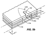
図5bは、回路基板の端面の別の例を示す拡大図である。この図は、要素片160の可能な変形部のパターンを例示するものである。変形部160aは、回路基板のトリミングの結果、図5aに例示のようにZ方向に延伸するだけでなく、X軸に沿って横方向に、および、Y軸に沿って空隙部112aの中へ延伸することも考えられる。どの変形部160aも空隙部112aや114aの中へ落ち込み、導電層112や114の端部112bと接触しなくなるように、空隙部112aは十分に広く(すなわち、X軸に沿って)作られる。同様に、メモリカード100の中へ入り込むいずれの変形部も空隙部112aや114aの中へ落ち込み、導電層112や114と接触しなくなるように、空隙部112aは十分に深く(すなわち、Y軸に沿って)作られる。図5bには変形部160aが層112まで延伸する状態だけが示されている。しかし、変形部160aは、層114まで延伸し、それによって、端部114bと接触せずに空隙部114aの中へ落ち込むことも考えられる。
FIG. 5 b is an enlarged view showing another example of the end face of the circuit board. This figure illustrates the pattern of possible deformations of the
図5cは、回路基板の端面の別の例を示す拡大図である。この例では、回路基板の端面で回路基板の層のすべてに溝がつけられている。溝116c、112c、114cは、それぞれ、絶縁層116、導電層112、導電層114に形成される。これらの溝は、図示されていない層および番号をつけられていない層を含む回路基板のすべての層の中を通る。溝116c、112c、114cは、X、Yの両方向に、導電層112と114の空隙部112aと114aよりも狭い。したがって、空隙部112aと114aは、溝112cと114cのいずれの側でも横方向(すなわち、X方向に)に延伸する。また、空隙部112aと114aは、溝112cと114cよりも深く(すなわち、Y方向に)延伸する。したがって、これらの溝は、上記空隙部の範囲内に形成され、上記空隙部によって完全に囲まれる。図5aと5bの前の例の場合と同様、生じる可能性があるどの変形部160aも、導電層112と114の端部112bや114bと接触せずに空隙部112aと114aの中へ落ち込むことになる。この結果、短絡が防止される。導電層112と114の空隙部が、該空隙部が中心位置合わせを行う対象とする導電性要素片160よりもXおよびY方向に広いかぎり、端面のジオメトリには、特に、溝116、112、114には多くの様々な変形例が存在することが考えられる。
FIG. 5c is an enlarged view showing another example of the end face of the circuit board. In this example, all the layers of the circuit board are grooved at the end face of the circuit board. The
図6cは、図5cに示す回路基板の断面A−Aに沿って切り取られた断面図である。図6aに関して上述したように、剪断処理あるいは切断処理中に絶縁層116の導電性要素片160が変形し、そのため、要素片160の変形部160aが回路基板の端面の下方へ延伸することになる。変形の量、したがって変形部160aの大きさは、剪断力、剪断器具のジオメトリおよび導電性要素片の金属の弾性に左右される。この変形部は、回路基板の端面の下方へ(すなわち、Z方向に)延伸したり、基板の端面を出たり入ったり(すなわち、Y方向に)、基板の端面を横切ったり(すなわち、X方向に)する可能性があることが予想される。したがって、空隙部112aが十分な広さでつくられているため、X方向のどのような量の変形部もこの空隙部の中へ落ち込むようになっていて、この変形部が端部112bや114bと接触することはない。空隙部112aが十分な深さでつくられているため、この空隙部の中へ(あるいは、Y方向に)延伸するどの変形部も同様に導電層112や導電層114と接触することはない。
6c is a cross-sectional view taken along section AA of the circuit board shown in FIG. 5c. As described above with respect to FIG. 6a, the
図8は、空隙部112aが持ち得る種々の形状のいくつかを示す図である。空隙部112aは、多くの異なる大きさと形状とを持つことが可能であり、これらの大きさと形状のすべては、変形部160aと導電層112や114との間のどのような短絡も防止できるほど十分な比例する広さを持つものである。
FIG. 8 is a diagram showing some of the various shapes that the
以上本発明の一例を例示して、説明してきたが、本発明に関係する当業者が、別の修正例、変更例および変形例をつくったり、思いついたりすることも可能であることは明らかである。 Although an example of the present invention has been illustrated and described above, it is obvious that those skilled in the art related to the present invention can make or come up with other modifications, changes, and variations. is there.
したがって、本発明が、以上図示して、説明してきた実施形態に限定されるものではないこと、並びに、本発明の本質的特徴を構成する特徴が組み込まれたような上記のような修正および別の実施形態のいずれも本発明の真の精神と範囲に属する均等なものであると考えられることが想定されている。 Accordingly, the present invention is not limited to the embodiments shown and described above, and modifications and alternatives such as those described above incorporating features that constitute essential features of the invention. It is envisioned that any of these embodiments are considered equivalent within the true spirit and scope of the present invention.
Claims (15)
回路基板の前記端面に導電性要素片を持つ第1の導電層と、
第1の絶縁層と、
前記第1の絶縁層により前記第1の導電層から分離され、前記第1の導電層の下方に位置して、前記回路基板の端面まで延伸する第2の導電層であって、前記第2の導電層が前記回路基板の端面に空隙部を持ち、前記空隙部の1以上の空隙部と前記導電性要素片の中心位置合わせを行うことにより、前記第2の導電層の側壁の端面まで延伸する前記導電性要素片のいずれの変形部も前記空隙部の範囲内にあり、前記第2の導電層とは非接触である、第2の導電層と、
を有する回路基板。A circuit board having at least one peripheral end face,
A first conductive layer having conductive element pieces on the end face of the circuit board;
A first insulating layer;
A second conductive layer that is separated from the first conductive layer by the first insulating layer, is positioned below the first conductive layer, and extends to an end surface of the circuit board; The conductive layer has a gap on the end face of the circuit board, and by aligning one or more gaps of the gap with the center of the conductive element piece, the end face of the side wall of the second conductive layer is reached. Any deformed portion of the conductive element piece to be stretched is within the range of the void, and is in non-contact with the second conductive layer; and
A circuit board.
前記空隙部が、溝である回路基板。The circuit board according to claim 1,
A circuit board in which the gap is a groove.
前記空隙部が、ノッチである回路基板。The circuit board according to claim 1,
A circuit board in which the gap is a notch.
前記空隙部の幅は、前記端面から離れるにしたがって前記空隙部が前記回路基板の端面よりも狭くなっている回路基板。The circuit board according to claim 1,
The width of the gap portion is a circuit board in which the gap portion is narrower than the end face of the circuit board as the distance from the end face increases.
前記第2の導電層が、接地層または電源層である回路基板。The circuit board according to claim 1,
A circuit board in which the second conductive layer is a ground layer or a power supply layer.
第3の導電層をさらに有する回路基板であって、前記第3の導電層が前記回路基板の端面に空隙部を持ち、前記空隙部と前記導電性要素片の中心位置合わせを行うことにより、前記第3の導電層の側壁の端面まで延伸する前記導電性要素片のいずれの変形部も前記空隙部の範囲内にあり、前記第3の導電層とは非接触である回路基板。The circuit board according to claim 1,
A circuit board further comprising a third conductive layer, wherein the third conductive layer has a gap at an end face of the circuit board, and the gap and the conductive element piece are aligned at the center, A circuit board in which any deformed portion of the conductive element piece extending to the end face of the side wall of the third conductive layer is within the range of the gap and is not in contact with the third conductive layer.
前記第3の導電層が、接地層または電源層である回路基板。The circuit board according to claim 6,
A circuit board in which the third conductive layer is a ground layer or a power supply layer.
前記回路基板の少なくとも1つの端面に沿って配置された導電性要素片を持つ第1の導電層を形成するステップと、
前記第1の導電層の下方に絶縁層を形成するステップと、
前記第1の導電層と前記絶縁層の下方に第2の導電層を形成するステップであって、前記第2の導電層が、前記回路基板の少なくとも1つの端面に沿って配置された空隙部を持ち、前記空隙部のうちの少なくとも1つの空隙部の方が前記導電性要素片よりも広く、さらに、前記空隙部と前記導電性要素片との中心位置合わせを行うステップと、
前記回路基板と前記導電性要素片とのトリミングを行って、前記導電性要素片のどの変形部も前記空隙部の中へ延伸し、前記第2の導電層とは非接触であるトリミングするステップと、
を有する方法。A method for making a multilayer circuit board, comprising:
Forming a first conductive layer having conductive element pieces disposed along at least one end face of the circuit board;
Forming an insulating layer below the first conductive layer;
Forming a second conductive layer below the first conductive layer and the insulating layer, wherein the second conductive layer is disposed along at least one end surface of the circuit board; And at least one of the gaps is wider than the conductive element piece, and the centering of the gap and the conductive element piece is performed.
Trimming the circuit board and the conductive element piece to extend any deformed portion of the conductive element piece into the gap, and to perform trimming that is not in contact with the second conductive layer When,
Having a method.
前記回路基板をトリミングするステップが、前記回路基板を剪断するステップを有する方法。The method of claim 8, wherein
The method of trimming the circuit board comprises shearing the circuit board.
前記第2の導電層の前に前記第1の導電層を剪断する方法。The method of claim 9, wherein
A method of shearing the first conductive layer before the second conductive layer.
前記回路基板の端面は、前記金属層の前記第1の領域が前記回路基板の第1の層を形成し、さらに、前記バスを前記第1の領域と接続する前記金属層の導電性要素片が前記回路基板の少なくとも前記1つの端面に位置し、前記回路基板の少なくとも1つの端面にわたって前記少なくとも1つのバスまで前記導電性要素片が延伸する少なくとも1つの端面と、
前記金属層の下方に在る絶縁層と、
前記金属層と前記絶縁層の下方に位置し、前記少なくとも1つの端面まで延伸する第2の導電層であって、前記第2の導電層が前記回路基板の前記少なくとも1つの端面に空隙部を持つことにより、前記空隙部のうちの少なくとも1つの空隙部と前記少なくとも1つの導電性要素片との中心位置合わせが行われる第2の導電層と、を有する回路基板の構造において、
前記第2の導電層の側壁の少なくとも1つの端面まで延伸する前記導電性要素片のいずれの変形部も前記空隙部の範囲内にあり、前記第2の導電層とは非接触である回路基板の構造。A circuit board structure having a metal layer comprising at least one bus, a first region, and a conductive element piece connecting the at least one bus to the first region,
The end face of the circuit board has the first region of the metal layer forming the first layer of the circuit board, and further the conductive element piece of the metal layer connecting the bus to the first region Is located on at least one end face of the circuit board, and at least one end face from which the conductive element piece extends to the at least one bus over at least one end face of the circuit board;
An insulating layer under the metal layer;
A second conductive layer positioned below the metal layer and the insulating layer and extending to the at least one end surface, wherein the second conductive layer has a gap in the at least one end surface of the circuit board; In the structure of the circuit board having a second conductive layer in which center alignment of at least one of the gaps and the at least one conductive element piece is performed,
A circuit board in which any deformed portion of the conductive element piece extending to at least one end face of the side wall of the second conductive layer is within the space and is not in contact with the second conductive layer. Structure.
前記空隙部が、溝である回路基板の構造。The structure of a circuit board according to claim 11 ,
A circuit board structure in which the gap is a groove.
第1の領域と、バスと、前記回路基板の端面において前記第1の領域を前記バスと接続する複数の導電性要素片とを有する第1の金属層を形成するステップであって、前記第1の領域が前記回路基板内に配置され、前記バスが前記回路基板外に配置されるように形成するステップと、
前記第1の金属層の前記第1の領域の下方に絶縁層を形成するステップと、
前記絶縁層の下方に、かつ、前記絶縁層により前記第1の金属層から分離して第2の金属層を形成するステップであって、前記第2の金属層が前記回路基板の端面まで延伸し、前記複数の導電性要素片の下方に配置された、前記回路基板の端面に複数の空隙部を有するように形成するステップと、
前記回路基板の端面において前記複数の導電性要素片を剪断し、前記バスを取り除いて、前記導電性要素片のいずれの変形部も前記第2の金属層の空隙部の範囲内に入るようにするステップと、
を有する方法。A method of providing a circuit board, a cover, and a memory storage device having a joint between an end face of the circuit board and the cover,
Forming a first metal layer having a first region, a bus, and a plurality of conductive element pieces connecting the first region to the bus at an end surface of the circuit board, Forming a region of 1 within the circuit board and the bus being disposed outside the circuit board;
Forming an insulating layer below the first region of the first metal layer;
Forming a second metal layer below the insulating layer and separated from the first metal layer by the insulating layer, the second metal layer extending to an end surface of the circuit board; And forming the plurality of gaps on the end face of the circuit board, which is disposed below the plurality of conductive element pieces,
The plurality of conductive element pieces are sheared at the end face of the circuit board, and the bus is removed, so that any deformed portion of the conductive element pieces falls within the gap of the second metal layer. And steps to
Having a method.
前記カバーの中へ前記回路基板を配置することによって、前記回路基板の端面と、前記第2の金属層の端面が前記カバーと前記回路基板との間の接合部に在るように為すステップとをさらに有する方法。14. The method of claim 13 , wherein
Placing the circuit board into the cover so that the end face of the circuit board and the end face of the second metal layer are at a joint between the cover and the circuit board; A method further comprising:
フラッシュメモリ、回路配線および受動素子を備える少なくとも1つの集積回路をさらに有する回路基板。The circuit board according to claim 1,
A circuit board further comprising at least one integrated circuit comprising flash memory, circuit wiring and passive elements.
Applications Claiming Priority (2)
| Application Number | Priority Date | Filing Date | Title |
|---|---|---|---|
| US09/921,664 US6597061B1 (en) | 2001-08-03 | 2001-08-03 | Card manufacturing technique and resulting card |
| PCT/US2002/024535 WO2003015484A1 (en) | 2001-08-03 | 2002-08-02 | Card manufacturing technique and resulting card |
Related Child Applications (1)
| Application Number | Title | Priority Date | Filing Date |
|---|---|---|---|
| JP2009158364A Division JP5222238B2 (en) | 2001-08-03 | 2009-07-03 | Card manufacturing method and resulting card |
Publications (3)
| Publication Number | Publication Date |
|---|---|
| JP2004538655A JP2004538655A (en) | 2004-12-24 |
| JP2004538655A5 JP2004538655A5 (en) | 2006-08-31 |
| JP4366187B2 true JP4366187B2 (en) | 2009-11-18 |
Family
ID=25445776
Family Applications (2)
| Application Number | Title | Priority Date | Filing Date |
|---|---|---|---|
| JP2003520256A Expired - Fee Related JP4366187B2 (en) | 2001-08-03 | 2002-08-02 | Card manufacturing method and resulting card |
| JP2009158364A Expired - Fee Related JP5222238B2 (en) | 2001-08-03 | 2009-07-03 | Card manufacturing method and resulting card |
Family Applications After (1)
| Application Number | Title | Priority Date | Filing Date |
|---|---|---|---|
| JP2009158364A Expired - Fee Related JP5222238B2 (en) | 2001-08-03 | 2009-07-03 | Card manufacturing method and resulting card |
Country Status (9)
| Country | Link |
|---|---|
| US (4) | US6597061B1 (en) |
| EP (1) | EP1413178B1 (en) |
| JP (2) | JP4366187B2 (en) |
| KR (1) | KR100924238B1 (en) |
| CN (1) | CN1290387C (en) |
| AT (1) | ATE454806T1 (en) |
| DE (1) | DE60235017D1 (en) |
| TW (1) | TW551022B (en) |
| WO (1) | WO2003015484A1 (en) |
Families Citing this family (26)
| Publication number | Priority date | Publication date | Assignee | Title |
|---|---|---|---|---|
| US6597061B1 (en) * | 2001-08-03 | 2003-07-22 | Sandisk Corporation | Card manufacturing technique and resulting card |
| JP3785083B2 (en) * | 2001-11-07 | 2006-06-14 | 株式会社東芝 | Semiconductor device, electronic card and pad rearrangement substrate |
| KR100660860B1 (en) | 2005-02-11 | 2006-12-26 | 삼성전자주식회사 | Malfunction prohibition device by surge voltage in integrated circuit and method thereof |
| US7654750B2 (en) * | 2005-08-10 | 2010-02-02 | Brenner Mary K | Bidirectional optical fiber link systems component couplers |
| DE102005041954A1 (en) * | 2005-09-03 | 2007-03-08 | Bayer Materialscience Ag | Alkoxysilane and special allophanate and / or biuret having prepolymers, a process for their preparation and their use |
| US20070117269A1 (en) * | 2005-11-19 | 2007-05-24 | Chin-Tong Liu | Method for packaging flash memory cards |
| US20070158799A1 (en) * | 2005-12-29 | 2007-07-12 | Chin-Tien Chiu | Interconnected IC packages with vertical SMT pads |
| TWI301984B (en) * | 2006-07-04 | 2008-10-11 | Orient Semiconductor Elect Ltd | Memory card with electrostatic discharge protection |
| JP2008166099A (en) * | 2006-12-28 | 2008-07-17 | Fuji Xerox Co Ltd | Circuit board and electronic component |
| US8928602B1 (en) | 2009-03-03 | 2015-01-06 | MCube Inc. | Methods and apparatus for object tracking on a hand-held device |
| US8797279B2 (en) | 2010-05-25 | 2014-08-05 | MCube Inc. | Analog touchscreen methods and apparatus |
| US8421082B1 (en) | 2010-01-19 | 2013-04-16 | Mcube, Inc. | Integrated CMOS and MEMS with air dielectric method and system |
| US8553389B1 (en) | 2010-08-19 | 2013-10-08 | MCube Inc. | Anchor design and method for MEMS transducer apparatuses |
| US8477473B1 (en) | 2010-08-19 | 2013-07-02 | MCube Inc. | Transducer structure and method for MEMS devices |
| US8476129B1 (en) | 2010-05-24 | 2013-07-02 | MCube Inc. | Method and structure of sensors and MEMS devices using vertical mounting with interconnections |
| US8710597B1 (en) | 2010-04-21 | 2014-04-29 | MCube Inc. | Method and structure for adding mass with stress isolation to MEMS structures |
| US8936959B1 (en) | 2010-02-27 | 2015-01-20 | MCube Inc. | Integrated rf MEMS, control systems and methods |
| US8794065B1 (en) | 2010-02-27 | 2014-08-05 | MCube Inc. | Integrated inertial sensing apparatus using MEMS and quartz configured on crystallographic planes |
| US8367522B1 (en) * | 2010-04-08 | 2013-02-05 | MCube Inc. | Method and structure of integrated micro electro-mechanical systems and electronic devices using edge bond pads |
| US8869616B1 (en) | 2010-06-18 | 2014-10-28 | MCube Inc. | Method and structure of an inertial sensor using tilt conversion |
| TWI388248B (en) * | 2010-06-25 | 2013-03-01 | Pegatron Corp | Electronic device |
| TWI525782B (en) * | 2011-01-05 | 2016-03-11 | 矽品精密工業股份有限公司 | Semiconductor package and fabrication method thereof |
| US8969101B1 (en) | 2011-08-17 | 2015-03-03 | MCube Inc. | Three axis magnetic sensor device and method using flex cables |
| US9603255B2 (en) | 2015-02-20 | 2017-03-21 | Nextgin Technology Bv | Method for producing a printed circuit board |
| CN114980523A (en) * | 2016-08-19 | 2022-08-30 | 奈科斯特金技术私人有限公司 | Method for manufacturing printed circuit board |
| US11234325B2 (en) | 2019-06-20 | 2022-01-25 | Infinera Corporation | Printed circuit board having a differential pair routing topology with negative plane routing and impedance correction structures |
Family Cites Families (20)
| Publication number | Priority date | Publication date | Assignee | Title |
|---|---|---|---|---|
| FR2076471A5 (en) | 1970-01-16 | 1971-10-15 | Bull General Electric | |
| EP0340492A3 (en) * | 1988-05-02 | 1990-07-04 | International Business Machines Corporation | Conformal sealing and interplanar encapsulation of electronic device structures |
| JPH0752784B2 (en) | 1988-05-24 | 1995-06-05 | 松下電工株式会社 | Printed wiring board |
| US5182632A (en) * | 1989-11-22 | 1993-01-26 | Tactical Fabs, Inc. | High density multichip package with interconnect structure and heatsink |
| JP2987182B2 (en) | 1990-09-04 | 1999-12-06 | イビデン株式会社 | Printed wiring board |
| US5138115A (en) * | 1990-10-12 | 1992-08-11 | Atmel Corporation | Carrierles surface mounted integrated circuit die |
| US5530376A (en) * | 1993-08-25 | 1996-06-25 | Sunright Limited | Reusable carrier for burn-in/testing of non packaged die |
| US5572140A (en) * | 1993-08-25 | 1996-11-05 | Sunright Limited | Reusable carrier for burn-in/testing on non packaged die |
| JPH09270325A (en) * | 1996-03-29 | 1997-10-14 | Tokin Corp | Electronic part |
| JP3012816B2 (en) * | 1996-10-22 | 2000-02-28 | 松下電子工業株式会社 | Resin-sealed semiconductor device and method of manufacturing the same |
| JP3942684B2 (en) | 1997-02-27 | 2007-07-11 | ユー・エム・シー・ジャパン株式会社 | Burn-in board |
| KR100214560B1 (en) * | 1997-03-05 | 1999-08-02 | 구본준 | Semiconductor multi chip module |
| KR100246587B1 (en) * | 1997-09-19 | 2000-03-15 | 유무성 | Ball grid array semiconductor package |
| US6072322A (en) * | 1997-12-30 | 2000-06-06 | Intel Corporation | Thermally enhanced test socket |
| US6351034B1 (en) * | 1998-06-01 | 2002-02-26 | Micron Technology, Inc. | Clip chip carrier |
| US6040622A (en) | 1998-06-11 | 2000-03-21 | Sandisk Corporation | Semiconductor package using terminals formed on a conductive layer of a circuit board |
| US6283770B1 (en) * | 1998-12-11 | 2001-09-04 | Cisco Technology, Incc. | Minimal intrusion EMI shielding clip to maintain electrical contact between two parallel surfaces |
| US6507117B1 (en) * | 1999-01-29 | 2003-01-14 | Rohm Co., Ltd. | Semiconductor chip and multichip-type semiconductor device |
| US6597061B1 (en) * | 2001-08-03 | 2003-07-22 | Sandisk Corporation | Card manufacturing technique and resulting card |
| TWI265611B (en) * | 2003-03-11 | 2006-11-01 | Siliconware Precision Industries Co Ltd | Semiconductor package with heatsink |
-
2001
- 2001-08-03 US US09/921,664 patent/US6597061B1/en not_active Expired - Lifetime
-
2002
- 2002-08-02 JP JP2003520256A patent/JP4366187B2/en not_active Expired - Fee Related
- 2002-08-02 DE DE60235017T patent/DE60235017D1/en not_active Expired - Lifetime
- 2002-08-02 KR KR1020047001332A patent/KR100924238B1/en not_active IP Right Cessation
- 2002-08-02 WO PCT/US2002/024535 patent/WO2003015484A1/en active Application Filing
- 2002-08-02 CN CNB028152859A patent/CN1290387C/en not_active Expired - Fee Related
- 2002-08-02 EP EP02750400A patent/EP1413178B1/en not_active Expired - Lifetime
- 2002-08-02 AT AT02750400T patent/ATE454806T1/en not_active IP Right Cessation
- 2002-08-05 TW TW091117584A patent/TW551022B/en not_active IP Right Cessation
-
2003
- 2003-06-06 US US10/456,077 patent/US7022547B2/en not_active Expired - Lifetime
-
2004
- 2004-11-12 US US10/987,626 patent/US7169640B2/en not_active Expired - Fee Related
-
2007
- 2007-01-08 US US11/621,051 patent/US20070111562A1/en not_active Abandoned
-
2009
- 2009-07-03 JP JP2009158364A patent/JP5222238B2/en not_active Expired - Fee Related
Also Published As
| Publication number | Publication date |
|---|---|
| JP5222238B2 (en) | 2013-06-26 |
| JP2009267434A (en) | 2009-11-12 |
| DE60235017D1 (en) | 2010-02-25 |
| EP1413178B1 (en) | 2010-01-06 |
| US20030209794A1 (en) | 2003-11-13 |
| TW551022B (en) | 2003-09-01 |
| JP2004538655A (en) | 2004-12-24 |
| US20070111562A1 (en) | 2007-05-17 |
| KR20040032873A (en) | 2004-04-17 |
| US6597061B1 (en) | 2003-07-22 |
| CN1290387C (en) | 2006-12-13 |
| EP1413178A1 (en) | 2004-04-28 |
| CN1539255A (en) | 2004-10-20 |
| ATE454806T1 (en) | 2010-01-15 |
| KR100924238B1 (en) | 2009-10-30 |
| WO2003015484A1 (en) | 2003-02-20 |
| US7022547B2 (en) | 2006-04-04 |
| US20050090038A1 (en) | 2005-04-28 |
| US7169640B2 (en) | 2007-01-30 |
Similar Documents
| Publication | Publication Date | Title |
|---|---|---|
| JP5222238B2 (en) | Card manufacturing method and resulting card | |
| RU2193231C2 (en) | Integrated-circuit module to be implanted in card body with built-in microprocessor (alternatives) | |
| US6222270B1 (en) | Integrated circuit bonding pads including closed vias and closed conductive patterns | |
| US20070270040A1 (en) | Chamfered Memory Card | |
| US7022552B2 (en) | Semiconductor device and method for fabricating semiconductor device | |
| KR101580925B1 (en) | Chip On Board Type Package | |
| US6855891B2 (en) | Card edge connector, method of manufacturing same, electronic card and electronic equipment | |
| KR20090079924A (en) | Edge connect wafer level stacking | |
| US20060118926A1 (en) | Semiconductor package, memory card including the same, and mold for fabricating the memory card | |
| JPH10335398A (en) | Multi-layer test-pad on semiconductor wafer and formation thereof | |
| JP2004165161A (en) | Plug connecting device, contact pin for plug connecting device and receptacle element for plug connecting device | |
| US6515374B1 (en) | Contact connection of metal interconnects of an integrated semiconductor chip | |
| US6484291B1 (en) | Library for storing pattern shape of connecting terminal and semiconductor circuit designed with different design rules | |
| US7837120B1 (en) | Modular memory card and method of making same | |
| CN105449395A (en) | Card connector | |
| CN106298558A (en) | Semiconductor packages and manufacture method thereof including insert | |
| CN111211118A (en) | Semiconductor device and semiconductor chip | |
| US6690088B2 (en) | Integrated circuit package stacking structure | |
| JP2005293146A (en) | Semiconductor memory card | |
| JPS6230095A (en) | Integrated circuit card | |
| KR20220006253A (en) | Semiconductor device and method for fabricating the same | |
| JP4448674B2 (en) | Chip tray | |
| JP6442003B1 (en) | IC card and IC card manufacturing method | |
| KR101376487B1 (en) | Interposer chip, method of manufacturing the interposer chip, and multi-chip package having the interposer chip | |
| JP4425712B2 (en) | Circuit board |
Legal Events
| Date | Code | Title | Description |
|---|---|---|---|
| A621 | Written request for application examination |
Free format text: JAPANESE INTERMEDIATE CODE: A621 Effective date: 20050629 |
|
| A521 | Request for written amendment filed |
Free format text: JAPANESE INTERMEDIATE CODE: A523 Effective date: 20060703 |
|
| A131 | Notification of reasons for refusal |
Free format text: JAPANESE INTERMEDIATE CODE: A131 Effective date: 20071016 |
|
| A521 | Request for written amendment filed |
Free format text: JAPANESE INTERMEDIATE CODE: A523 Effective date: 20080116 |
|
| A131 | Notification of reasons for refusal |
Free format text: JAPANESE INTERMEDIATE CODE: A131 Effective date: 20080708 |
|
| A521 | Request for written amendment filed |
Free format text: JAPANESE INTERMEDIATE CODE: A523 Effective date: 20081007 |
|
| A131 | Notification of reasons for refusal |
Free format text: JAPANESE INTERMEDIATE CODE: A131 Effective date: 20090407 |
|
| A521 | Request for written amendment filed |
Free format text: JAPANESE INTERMEDIATE CODE: A523 Effective date: 20090703 |
|
| TRDD | Decision of grant or rejection written | ||
| A01 | Written decision to grant a patent or to grant a registration (utility model) |
Free format text: JAPANESE INTERMEDIATE CODE: A01 Effective date: 20090728 |
|
| A01 | Written decision to grant a patent or to grant a registration (utility model) |
Free format text: JAPANESE INTERMEDIATE CODE: A01 |
|
| A61 | First payment of annual fees (during grant procedure) |
Free format text: JAPANESE INTERMEDIATE CODE: A61 Effective date: 20090824 |
|
| FPAY | Renewal fee payment (event date is renewal date of database) |
Free format text: PAYMENT UNTIL: 20120828 Year of fee payment: 3 |
|
| R150 | Certificate of patent or registration of utility model |
Free format text: JAPANESE INTERMEDIATE CODE: R150 |
|
| FPAY | Renewal fee payment (event date is renewal date of database) |
Free format text: PAYMENT UNTIL: 20120828 Year of fee payment: 3 |
|
| S111 | Request for change of ownership or part of ownership |
Free format text: JAPANESE INTERMEDIATE CODE: R313113 |
|
| FPAY | Renewal fee payment (event date is renewal date of database) |
Free format text: PAYMENT UNTIL: 20120828 Year of fee payment: 3 |
|
| R360 | Written notification for declining of transfer of rights |
Free format text: JAPANESE INTERMEDIATE CODE: R360 |
|
| FPAY | Renewal fee payment (event date is renewal date of database) |
Free format text: PAYMENT UNTIL: 20120828 Year of fee payment: 3 |
|
| R370 | Written measure of declining of transfer procedure |
Free format text: JAPANESE INTERMEDIATE CODE: R370 |
|
| S111 | Request for change of ownership or part of ownership |
Free format text: JAPANESE INTERMEDIATE CODE: R313113 |
|
| FPAY | Renewal fee payment (event date is renewal date of database) |
Free format text: PAYMENT UNTIL: 20120828 Year of fee payment: 3 |
|
| R350 | Written notification of registration of transfer |
Free format text: JAPANESE INTERMEDIATE CODE: R350 |
|
| FPAY | Renewal fee payment (event date is renewal date of database) |
Free format text: PAYMENT UNTIL: 20120828 Year of fee payment: 3 |
|
| FPAY | Renewal fee payment (event date is renewal date of database) |
Free format text: PAYMENT UNTIL: 20130828 Year of fee payment: 4 |
|
| LAPS | Cancellation because of no payment of annual fees |